

Sony CXA1279BS Datasheet
—1—
E99336-TE
Sony reserves the right to change products and specifications without prior notice. This information does not convey any license by
any implication or otherwise under any patents or other right. Application circuits shown, if any, are typical examples illustrating the
operation of the devices. Sony cannot assume responsibility for any problems arising out of the use of these circuits.
Absolute Maximum Ratings (Ta=25 °C)
• Supply voltage VCC 14 V
• Operating temperature Topr –20 to +75 °C
• Storage temperature Tstg –65 to +150 °C
• Allowable power dissipation
PD 900 mW
Operating Condition
Supply voltage VCC 8.5 to 12.5 V
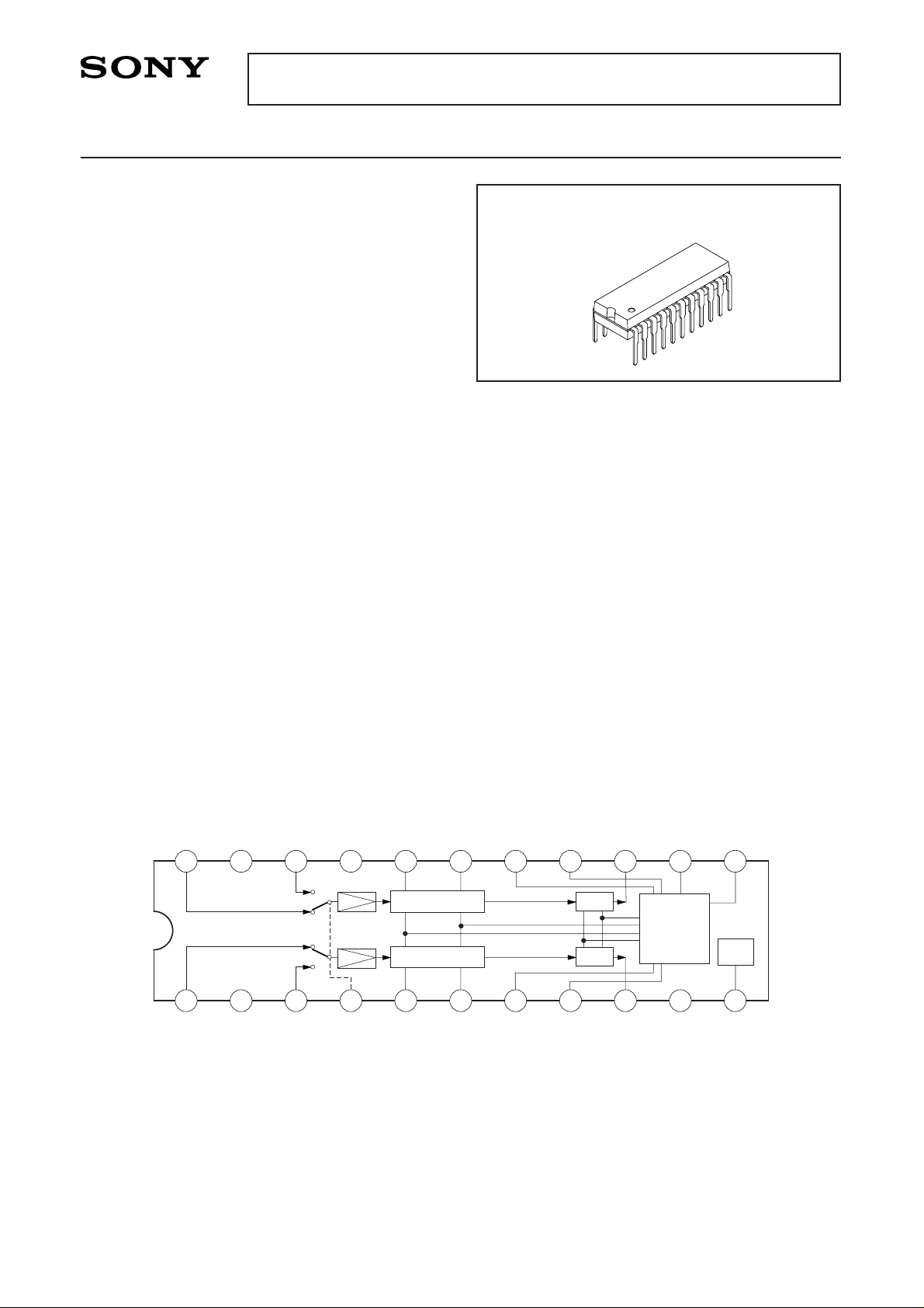
Description
The CXA1279BS is a bipolar IC for TV sound
control with functions such as tone control, volume
and balance.
Features
• 2 type of inputs
• Bass, Treble, Balance and Volume control operative
in either 0 to VCC or 0 to 5 V.
Applications
TV
Structure
Bipolar silicon monolithic IC
TV Sound Processor
22 pin SDIP (Plastic)
CXA1279BS
Block Diagram and Pin Configuration
REG
VCA
TVIN2
GND
AUXIN2
INSW
CH2
CL2
BASS
TREBLE
OUT2
N.C
VREG
TVIN1
V
CC
AUXIN1
N.C
CH1
CL1
VOLUME
BALANCE
OUT1
VRS
CREF
TONE
TONE
VCA
1 2 3 4 5 6 7 8 9
10 11
1213141516171819202122
CONTROL
&
BIAS
—2—
CXA1279BS
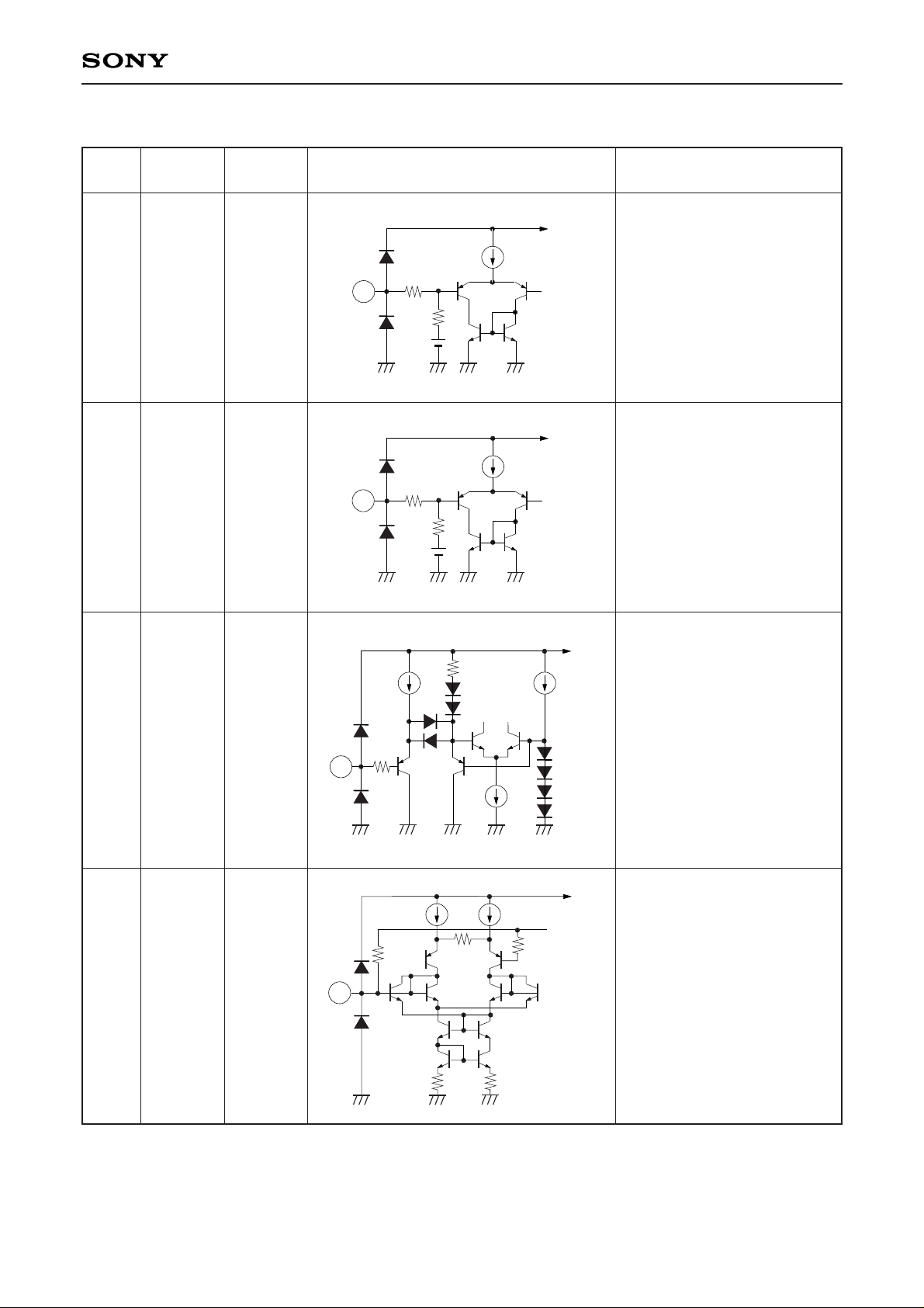
Pin
No.
1
3
4
5
Symbol
TV-IN2
AUX-IN2
INSW
CH2
3
36k
VCC/2
12k
V
CC
12µ
2k
V
CC
60µ
60µ
60µ
4
7k
2.7k
2.8k 2.8k
2.7k
VCC
180µ 180µ
5
Description
TV mode input pin.
AUX mode input pin.
Mode select pin.
External pin of HPF capacitor.
1
36k
VCC/2
12k
V
CC
12µ
Pin Description (Ta=25 °C VCC=9 V)
Voltage
4.5 V
4.5 V
—
4.5 V
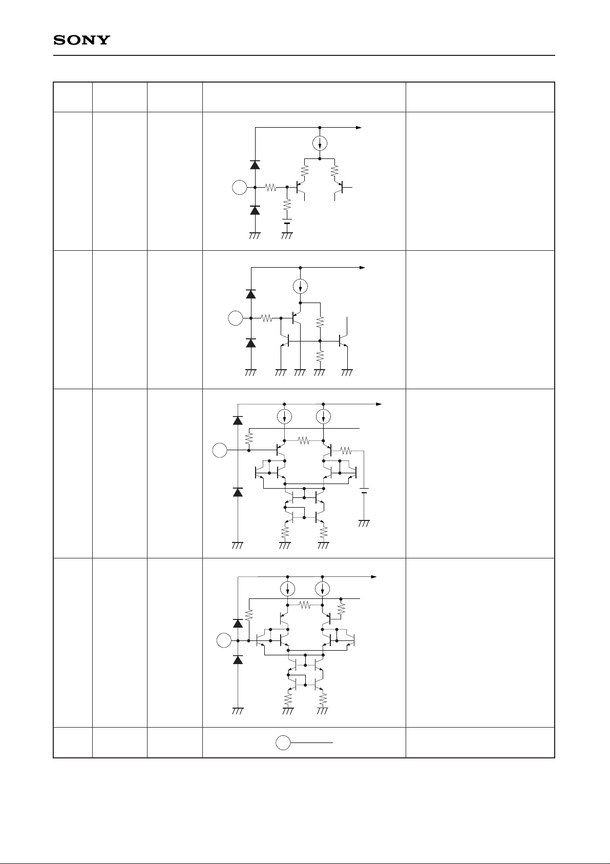
Equivalent circuit
—3—
CXA1279BS
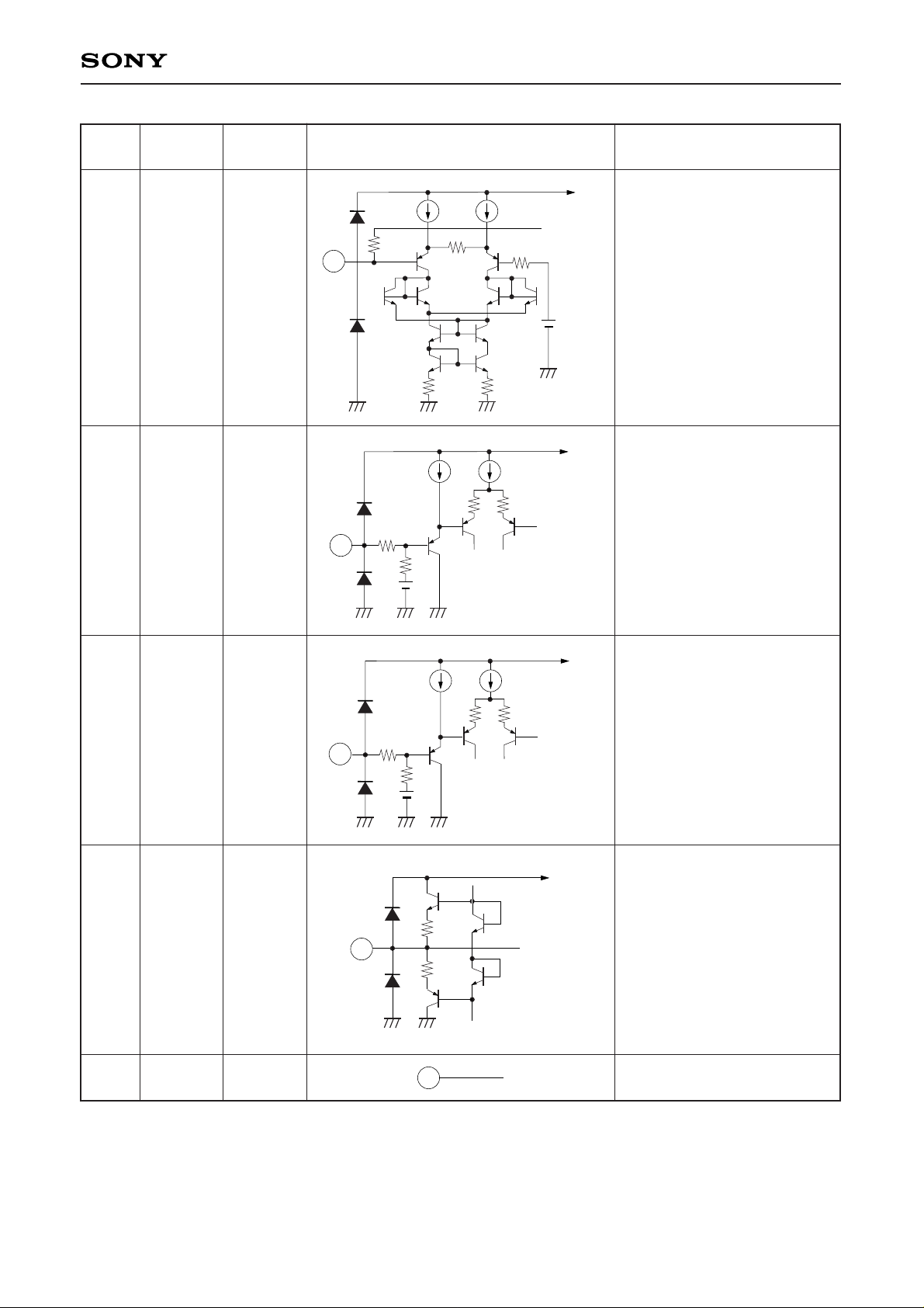
Pin
No.
6
7
8
9
10
Symbol
CL2
BASS
TREBLE
OUT2
N.C
5.2k
25k
20k
5.2k
V
CC
50µ CREF/20k
CREF
7
8
5.2k
25k
20k
5.2k
V
CC
50µ CREF/20k
CREF
500
500
V
CC
9
Description
External pin of LPF capacitor.
BASS control pin.
TREBLE control pin.
Output pin.
—
6.3k
2.8k
2.8k 2.8k
2.8k
4.5V
VCC
180µ 180µ
6
Voltage
4.5 V
4.5 V
(CREF)
4.5 V
(CREF)
4.5 V
—
Equivalent circuit
10
—4—
CXA1279BS
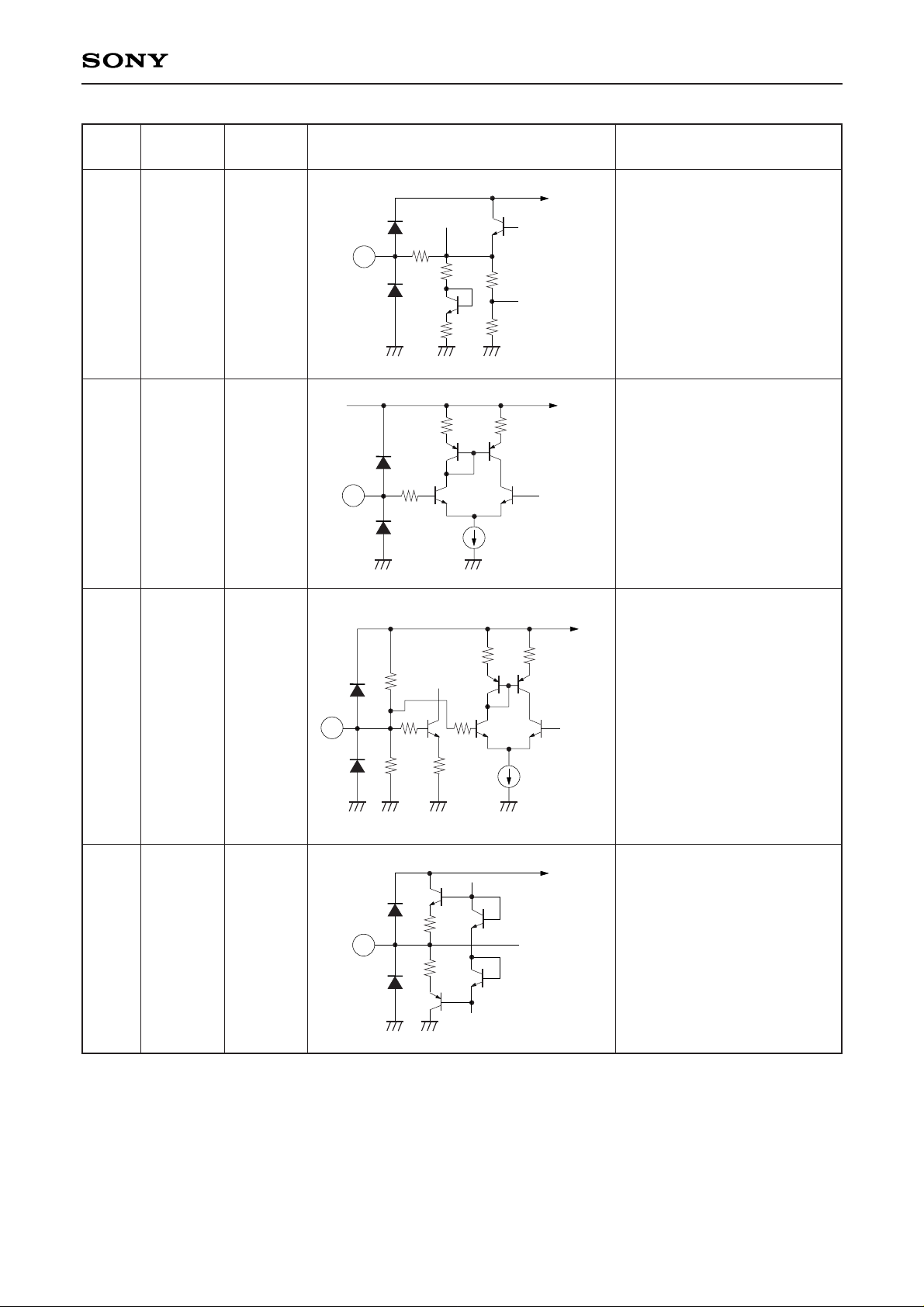
Pin
No.
11
12
13
14
Symbol
VREG
CREF
VRS
OUT1
1k
V
CC
30µ
12
1k
6k
V
CC
30µ
6k 15k
16k 16k
13
1k
500
500
V
CC
14
Description
REGULATOR output pin.
Input pin of control reference
voltage.
Reference voltage pin.
Voltage VCC/2.
Output pin.
120
VCC
11
Voltage
2.5 V
—
4.5 V
4.5 V
Equivalent circuit
—5—
CXA1279BS
Pin
No.
15
16
17
18
19
Symbol
BALANCE
VOLUME
CL1
CH1
N.C
47k
140µ
8k
10k
V
CC
16
6.3k
2.8k
2.8k 2.8k
2.8k
4.5V
VCC
180µ 180µ
17
7k
2.7k
2.8k 2.8k
2.7k
VCC
180µ 180µ
18
Description
BALANCE control pin.
VOLUME control pin.
External pin of LPF capacitor.
External pin of HPF capacitor.
—
25k
20k
5.2k 5.2k
V
CC
CREF/20k
CREF
15
Voltage
4.5 V
(CREF)
—
4.5 V
4.5 V
—
Equivalent circuit
19
 Loading...