Sony CXA1211M Datasheet

Electronic Volume
Description
The CXA1211M is a wide band general-purpose
VCA. This bipolar IC incorporates 2 chnannels.
Features
• Wide band frequency characteristics:
100kHz to 20MHz (–0.5dB)
• Wide dynamic range
• Low noise, low distortion
• Low power consumption
Applications
Video signals and other wide band VCA
Operating Conditions
Supply voltage VCC 4.50 to 5.50 V
Absolute Maximum Ratings
• Supply voltage VCC 14 V
• Operating temperature Topr –20 to +75 °C
• Storage temperature Tstg –65 to +150 °C
• Allowable power dissipation
PD 510 mW
Block Diagram and Pin Configuration
– 1 –
E90534D8X
Sony reserves the right to change products and specifications without prior notice. This information does not convey any license by
any implication or otherwise under any patents or other right. Application circuits shown, if any, are typical examples illustrating the
operation of the devices. Sony cannot assume responsibility for any problems arising out of the use of these circuits.
CXA1211M
8 pin SOP (Plastic)
2
3
4
1
5
6
7
8
IN1
CONT1
OUT1
GND
V
CC
IN2
CONT2
OUT2
VCA2
VCA1

– 2 –
CXA1211M
Pin Description
Pin
No.
1 IN1 2.5V
1.0Vp-p
∗
40kΩ
Signal input pin
(CH1)
Symbol
Voltage
DC AC
I/O
resistance
Equivalent circuit Description
VCC
GND
1
40k
3k
2 CONT1
2.7V
∗
—
Input pin of gain control signal
(CH1).
At "Low" power save is
possible.
Low: 1V and below
VCC
GND
24k25k
100µ 1µ 100µ
3 OUT1 1.9V
1.0Vp-p
Signal output pin
(CH1)
3
129
VCC
GND
1m
5 OUT2 1.9V
1.0Vp-p
Signal output pin
(CH2)
129
VCC
GND
1m
5
4
GND
0V
∗
— — —
GND pin
∗
External input

– 3 –
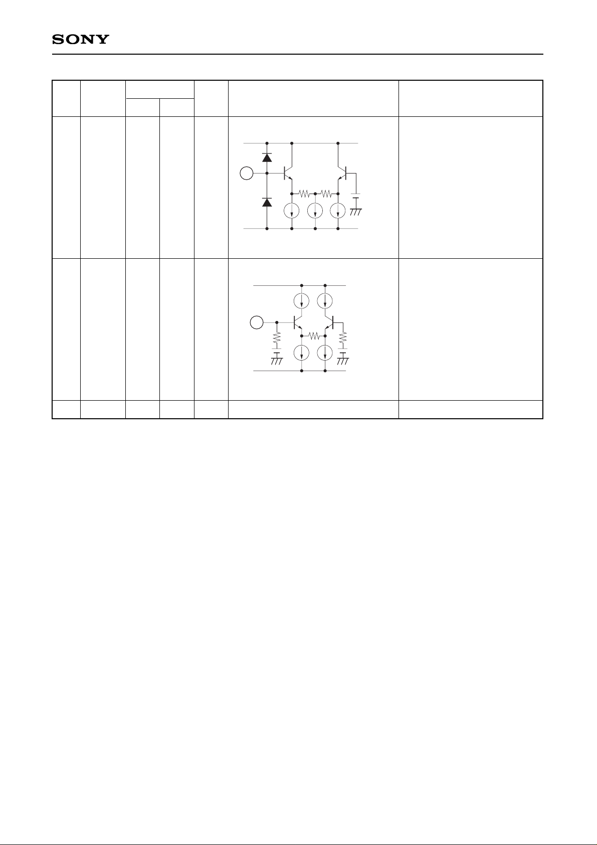
CXA1211M
Pin
No.
6 CONT2
2.7V
∗
—
Input pin of gain control signal
(CH2).
At "Low" power save is
possible.
Low: 1V and below
Symbol
Voltage
DC AC
I/O
resistance
Equivalent circuit Description
VCC
GND
24k 5k
100µ 1µ 100µ
6
7 IN2 2.5V
1.0Vp-p
∗
40kΩ
Signal input pin
(CH2)
VCC
GND
40k
3k
7
8 VCC
5V
∗
—
— —
VCC pin
∗
External input
 Loading...