

Sony CXA1202R, CXA1202Q-Z Datasheet

REC/PB Amplifier for VCR
Description
CXA1202Q-Z/CXA1202R are bipolar ICs developed
as REC/PB amplifiers for VCR's.
Features
• Built-in head amplifier feedback dumping con-
tributes to the reduction of external components
and simplification of the print circuit board design.
• Built-in BPF for PB signals medium range frequency
compensation totally eliminates external resonance
circuits (L. C. R.)
• Low range recording signal variable-level mix
amplifier allows for both metal powder and metal
evaporated tapes application.
• Consumption saving through power save function
of the REC AMP.
• 4-head system switch incorporated.
Functions
• Recording: 2-channel REC AMP, 5-input (Y, Chroma, AFM, ATF, PCM) Mix AMP.
• Playback: 2-channel low-noise head amplifier, medium range frequency compensation circuit, RF AGC,
dropout detecting circuit.
Structure
Bipolar silicon monolithic IC
Applications
• 8-mm system VCR
• β-system VCR
• VHS-system VCR
Absolute Maximum Ratings (Ta = 25°C)
• Supply voltage Vcc 8 V
• Operating temperature Topr –10 to +75 °C
• Storage temperature Tstg –55 to +150 °C
• Allowable power dissipation PD (CXA1202Q-Z) 920 mW
PD (CXA1202R) 1100 mW
(CXA1202R: Substrate area 40 × 25mm2, t = 0.635mm when ceramic print circuit board mounted)
Recommended Operating Condition
Supply voltage Vcc 5 ± 0.25 V
– 1 –
E88012-PS
Sony reserves the right to change products and specifications without prior notice. This information does not convey any license by
any implication or otherwise under any patents or other right. Application circuits shown, if any, are typical examples illustrating the
operation of the devices. Sony cannot assume responsibility for any problems arising out of the use of these circuits.
CXA1202Q-Z/CXA1202R
CXA1202Q-Z
48 pin QFP (Plastic)
CXA1202R
48 pin LQFP (Plastic)
For the availability of this product, please contact the sales office.
– 2 –
CXA1202Q-Z/CXA1202R
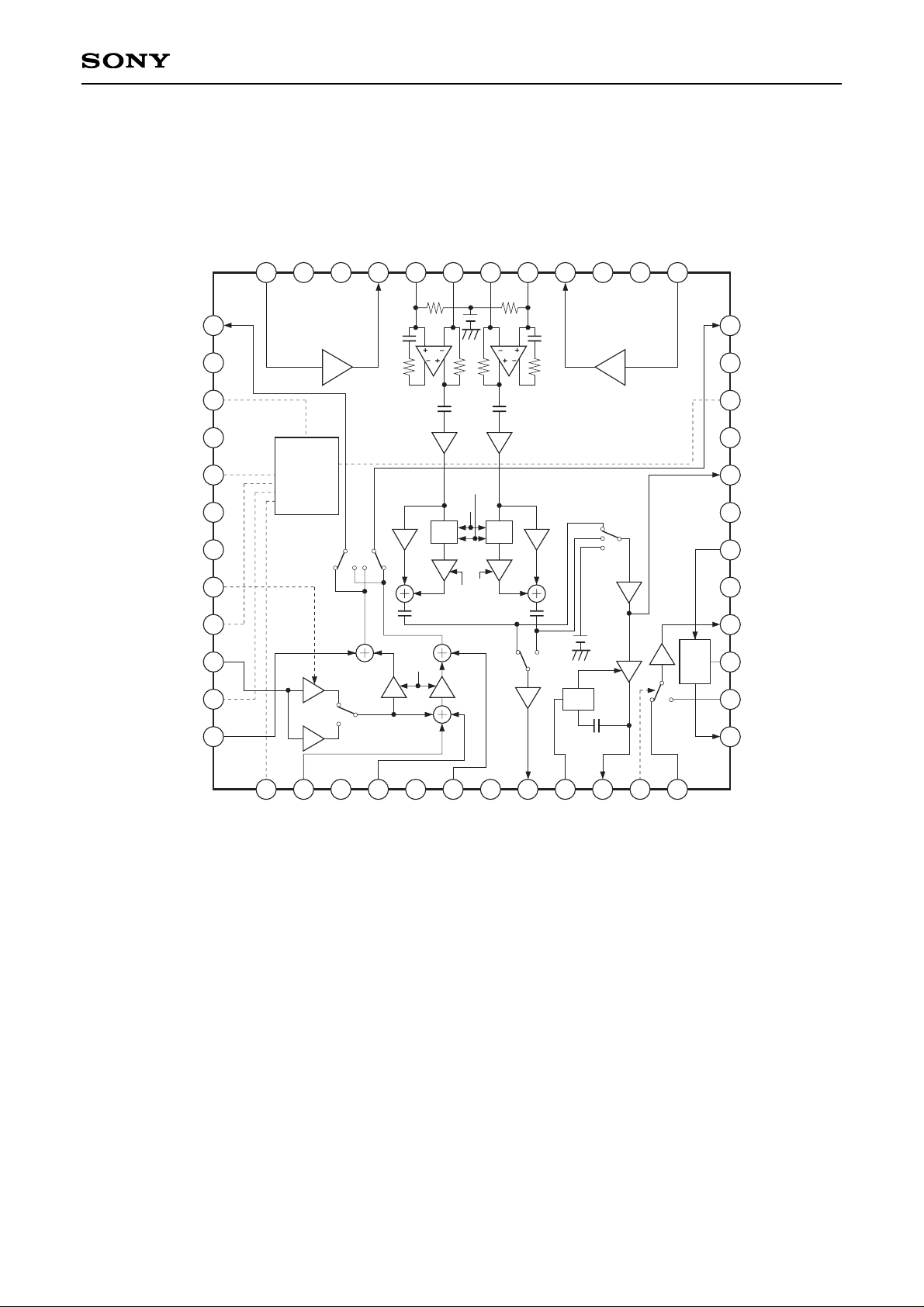
Block Diagram and Pin Configuration
ATF LEVEL
VCA
6dB
DOC
DET
BPF BPF
CONTROL
LOGIC
RP PB EN
C IN
VREG
AFM IN
VG
Y IN
V
CC
PCM RF OUT
AGC TC
AGC OUT
HCHG
RF IN A
2
3
4
5
6
7
8
9
10
12
1
MIX1 OUT
MT1
MULTI
GND 1CH
V RF OUT
GND PB
DOC IN
V
CC EF
RF OUT
DOC TC
RF IN B
DOC PULSE
13
14
15
16
17
18
19
20
21
22
23
24
MIX2 OUT
MT 2
RF SWP
GND 2CH
PCM SEL
ME LEVEL
GND REC
RP PB 1CH
ATF IN
RP PB 2CH
PCM IN
40
39
38
37
41
42
43
44
45
46
47
48
REC2 IN
MT Q
V
CC
2CH
REC2 OUT
PB IN 2P
PB IN 2N
PB IN 1N
PB IN 1P
REC1 OUT
V
CC
1CH
MT Fφ
REC1 IN
36
35
34
31
32
33
25
2627
28
29
30
CH2
REC AMP
CH1
REC AMP
CH1
HEAD AMP
46dB
9dB
CH2
HEAD AMP
46dB
9dB
VP2
SW
VP1
SW
P V P V
–6dB
MTFφ
MTQ
MT2
MT1
–6dB
CH2
CH1
Mute
Video
SW
6dB
DOC
DET
12dB
GCA
A B
RF SW
CH2 CH1
PCM
SW
MIX
AMP
6dB
RF
AGC
DET
11
ME
LEVEL
VCAVCA
ATF
SW
Medium range freq.
compensation
VCA VCA
Multi
Normal
– 3 –
CXA1202Q-Z/CXA1202R
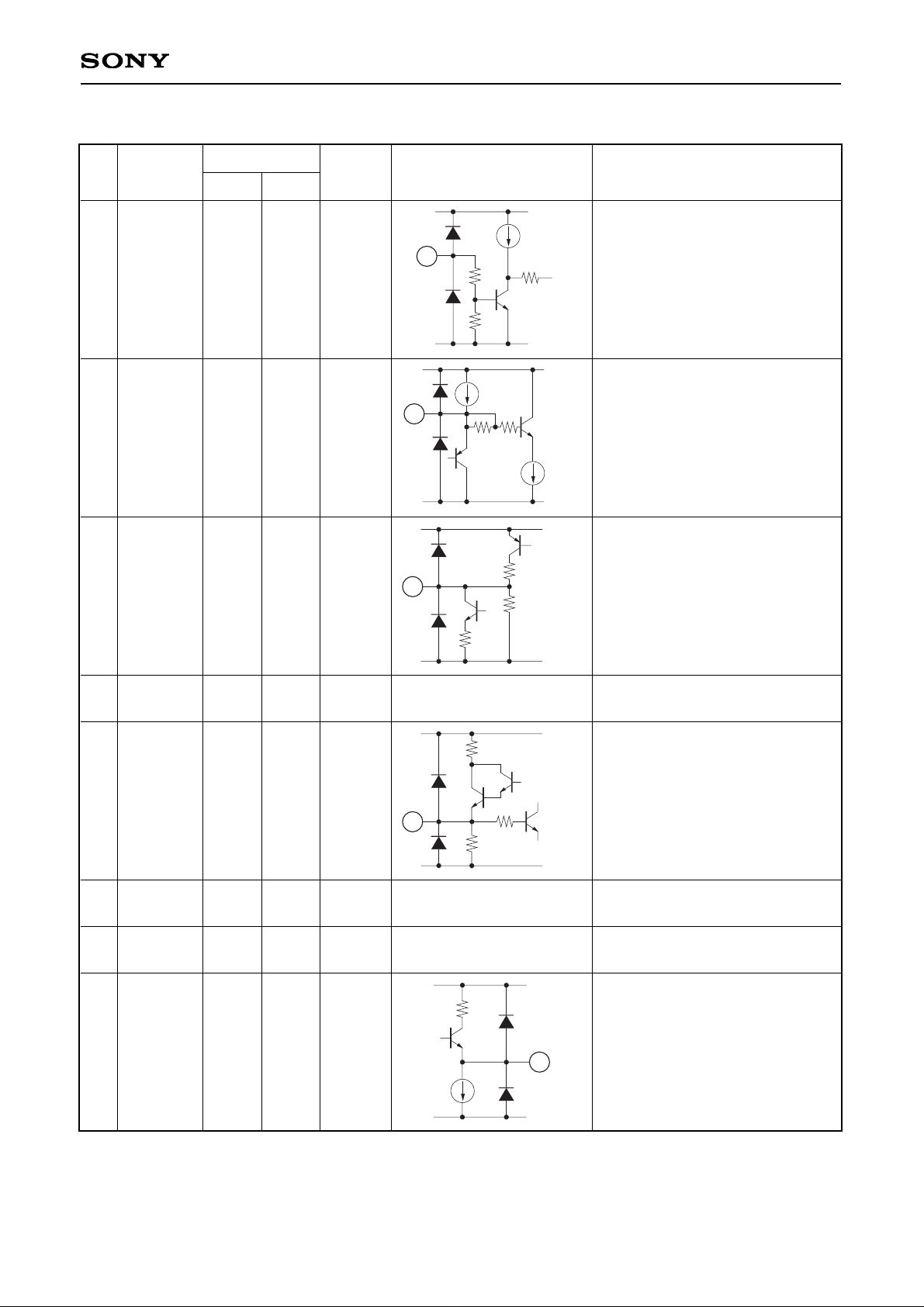
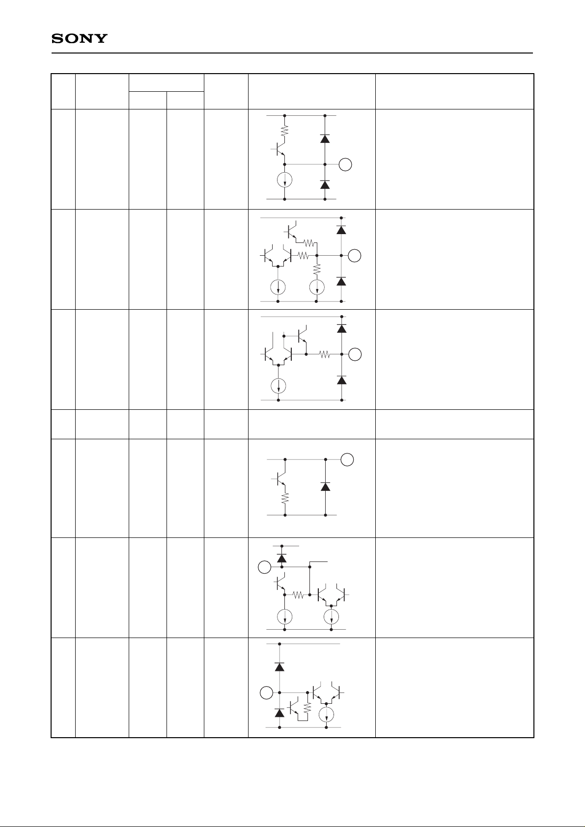
Pin Description
No.
1
2
3
4
5
6
7
8
RP PB EN
C IN
VREG
AFM IN
VG
Y IN
Vcc
PCM RF
OUT
(Open:
"L")
3.2V
4.2V
3.2V
2.5V
3.2V
5.0V
1.8V
—
134
mVp-p
—
80
mVp-p
—
250
mVp-p
—
50 to
500
mVp-p
40kΩ
20kΩ
—
20kΩ
—
20kΩ
—
Emitter
follower
(IE = 1mA)
Symbol
Equivalent circuit
Description
I/O
resistance
DC
AC
Voltage
1
V
CC
GND
40k
20k
VCC
GND
20k
2
100
VCC
GND
3
24k
35k
VCC
GND
2.5k
150
5
1mA
VCC
GND
8
440
Power-save recording at Low.
High: over 3V
Low: under 1V
Input pin for Chroma signal.
Output pin for VREG 4.2V.
Decoupling with capacitance.
Input pin for AFM signal.
Output pin for virtual GND.
Decoupling with capacitance.
Input pin for Y signal.
Supply pin for circuits other than
REC AMP and Head AMP.
Output pin for PB PCM signal.
Same as for Pin No. 2
Same as for Pin No. 2
—
– 4 –
CXA1202Q-Z/CXA1202R
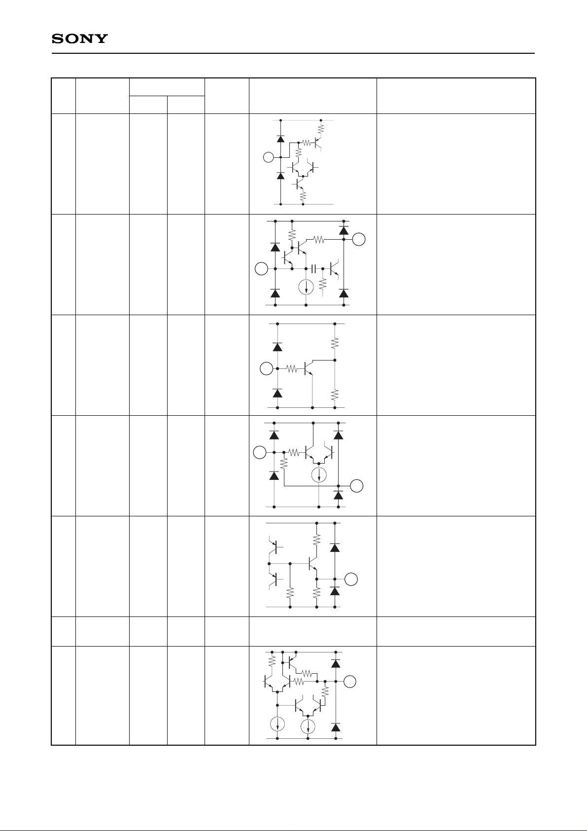
No.
9
10
11
12
13
14
15
AGC TC
AGC OUT
HCHG
RF IN A
DOC
PULSE
RF IN B
DOC TC
4.25V
(Load:
150kΩ
2.5V
—
(Open:
"L")
2.5V
H: 3.2V
L: 0V
2.5V
2.5V
—
100
mVp-p
—
100
mVp-p
—
100
mVp-p
—
—
Emitter
follower
(IE = 1mA)
50kΩ
—
Emitter
follower
(H: IE =
1mA)
20kΩ
—
Symbol
Equivalent circuit
Description
I/O
resistance
DC
AC
Voltage
VCC
500
200
GND
9
200
1mA
VCC
GND
200
10
17
VCC
GND
11
50k
VCC
GND
150
20k
5
12
VCC
GND
100
80k 3.5k
13
VCC
GND
90
8k
15
3.3k
Pin to apply time constant of
envelope detection for RF AGC.
Optimum load resistance across
Vcc is 150kΩ.
AGC output pin for PB VIDEO
signal (Max. gain of AGC AMP is
about 7dB).
Control signal input pin for RF SW
switching:
High (over 3V): selects RF IN A
Low (under 0.3V):
selects RF IN B
Input pin for RF switch and 12dB
AMP.
Dropout detection signal output
pin; High upon dropout.
Input pin for RF switch and 12dB
AMP.
Pin to connect time constant of
dropout detection.
Same as for Pin No. 12
– 5 –
CXA1202Q-Z/CXA1202R
No.
16
17
18
19
20
21
22
23
RF OUT
Vcc EF
DOC IN
GND PB
V RF OUT
GND 1CH
MULTI
MT1
2.5V
5.0V
2.5V
0V
1.8V
0V
—
(OPEN:
"L")
—
(2.5V
at
OPEN
of pin)
400
mVp-p
—
400
mVp-p
—
50 to
500
mVp-p
—
—
—
Emitter
follower
(IE =
500µA)
—
8kΩ
—
Emitter
follower
(IE =
500µA)
—
40kΩ
100kΩ
Symbol
Equivalent circuit
Description
I/O
resistance
DC
AC
Voltage
500µA
VCC
GND
200
16
VCC
GND
200
17
VCC
GND
150
8k
18
2.5V
VCC
GND
400
20
500µA
VCC
GND
25k
23
47k 53k
5
Output pin of signal selected by
HCHG from RF IN A and RF IN B.
Supply pin for emitter followers of
AGC OUT, DOC TC and RF OUT.
Input pin for dropout detection.
GND pin for medium range
frequency compensation circuit,
RF AGC and DOC DET.
Output pin for PB VIDEO signal.
GND pin for CH1 REC AMP and
CH1 Head AMP.
Multi-channel PCM REC mode at
High.
Boost level adjusting pin for CH1
medium range frequency
compensation circuit.
Variable between 0 and +12dB at
4.2 to 0.8V.
—
—
Same as for Pin No. 1
– 6 –
CXA1202Q-Z/CXA1202R
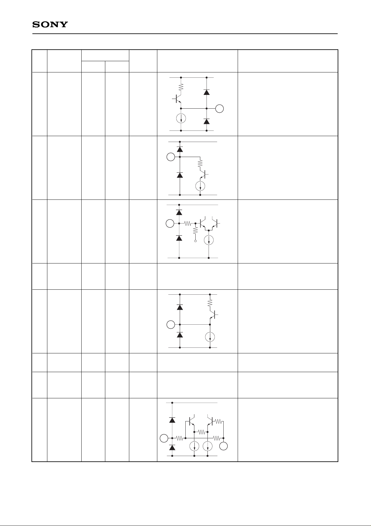
No.
24
25
26
27
28
29
30
MIX1 OUT
REC1 IN
MT Fφ
Vcc 1CH
REC1 OUT
PB IN 1P
PB IN 1N
2.5V
1.8V
2.5V
5.0V
15mA
2.4V
2.4V
203
mVp-p
92µA
(Y signal)
—
—
13
mAp-p
90 to
900
µVp-p
—
Emitter
follower
(IE = 1mA)
~
–
0
—
—
Open
collector
1.3kΩ
1.3kΩ
Symbol
Equivalent circuit
Description
I/O
resistance
DC
AC
Voltage
1mA
VCC
GND
400
24
VCC
GND
100
200
100
25
VCC
GND
90
26
GND
20
28
VCC
GND
10k
29
VCC
GND
30
Mix circuit output pin for CH1.
CH1 REC AMP input pin.
Fφ adjusting pin for medium range
frequency compensation circuit;
Fφ is controlled through current
value by connecting resistance
between GNDs. Mutually affected
by MT Q. Do not connect
capacitance.
Power supply pin for CH1 REC
AMP and CH1 Head AMP.
CH1 REC AMP output pin.
CH1 head AMP positive phase
input pin (PB signal input pin).
CH1 Head AMP inverter phase
input pin (decoupling with
capacitance).
—
– 7 –
CXA1202Q-Z/CXA1202R
No.
31
32
33
34
35
36
37
38
39
40
41
42
PB IN 2N
PB IN 2P
REC2 OUT
Vcc 2CH
MT Q
REC2 IN
MIX2 OUT
MT 2
RF SWP
GND 2CH
PCM SEL
ME LEVEL
2.4V
2.4V
15mA
5.0V
2.5V
1.8V
2.5V
—
(2.5V
at
OPEN
of pin)
—
(Open:
"L")
0V
—
(Open:
"L")
—
(2.1V
at
OPEN
of pin)
—
90 to
900
µVp-p
13
mAp-p
—
—
92µA
(Y signal)
203
mVp-p
—
—
—
—
—
1.3kΩ
1.3kΩ
—
—
~
–
0
Emitter
follower
(IE = 1mA)
100kΩ
40kΩ
—
40kΩ
100kΩ
Symbol
Equivalent circuit
Description
I/O
resistance
DC
AC
Voltage
VCC
GND
24k 76k
2.1V
18k
42
CH2 Head AMP Inverter phase
input pin (decoupling with
capacitance).
CH2 Head AMP positive phase
input pin (PB signal input pin).
CH2 REC AMP output pin.
Power supply pin for CH2 REC
AMP and CH2 Head AMP.
Q adjusting pin for medium range
frequency compensation circuit.
Controls Q through current value
by connecting resistance between
GNDs; Mutually effected by MT
Fφ. Do not connect capacitance.
CH2 REC AMP input pin.
Mix circuit output pin for CH2.
Boost level adjusting pin for CH2
medium range frequency
compensation circuit; variable
between 0 and +12dB at 4.2 to 0.8V.
RF switching pulse input pin for
CH switchover.
GND pin for CH2 REC AMP and
CH2 head AMP.
PCM AREA input pin;
High: PCM REC period
During High period after recording,
MUTE is applied to PB VIDEO
output.
Level of low range REC signals
(Chroma, AFM, ATF rec. with
VIDEO) can be boosted by 0 to
3dB by voltage (0 to 5V) applied
to this pin.
Same as for Pin No. 30
Same as for Pin No. 29
Same as for Pin No. 28
Same as for Pin No. 26
Same as for Pin No. 25
Same as for Pin No. 24
Same as for Pin No. 23
Same as for Pin No. 1
Same as for Pin No. 1
—
—
– 8 –
CXA1202Q-Z/CXA1202R
No.
43
44
45
46
47
48
GND REC
ATF
LEVEL
RP PB
1CH
ATF IN
RP PB
2CH
PCM IN
0V
—
(2.1V
at
OPEN
of pin)
—
(Open:
"L")
2.5V
—
(Open:
"L")
3.2V
—
—
—
250
mVp-p
—
250
mVp-p
—
100kΩ
40kΩ
20kΩ
40kΩ
20kΩ
Symbol
Equivalent circuit
Description
I/O
resistance
DC
AC
Voltage
VCC
GND
20k
100
5
46
GND pin for VG, VREG, LOGIC
and mix circuit.
REC Ievel of ATF signal can be
boosted by 0 to 3dB by the voltage
(0 to 5V) applied to this pin.
In multi PCM mode, priority given
to 6dB AMP.
REC/PB switchover signal for CH1:
High: PB
Low: REC
However, when RP PB EN pin is
at Low:
High: power save REC
Low: REC
Input pin for ATF pilot signal.
REC/PB switchover signal for CH2:
High: PB
Low: REC
However, when RP PB EN pin is
at Low:
High: power save REC
Low: REC
Input pin for PCM signal.
—
Same as for Pin No. 42
Same as for Pin No. 1
Same as for Pin No. 1
Same as for Pin No. 2
 Loading...