

Sony CXA1166K Datasheet
8-bit 250 MSPS Flash A/D Converter
Description
The CXA1166K is an 8-bit ultrahigh-speed flash
A/D converter IC capable of digitizing analog signals
at a maximum rate of 250 MSPS. The digital I/O
level of this A/D converter is compatible with the
ECL 100K/10KH/10K.
This IC is pin-compatible with the conventional
CXA1076AK/CXA1176K/CXA1176AK, and can
replace the conventional models easily. Compared
with the conventional models, the CXA1166K has a
greatly improved performance because of the new
circuit design and carefully considered layout.
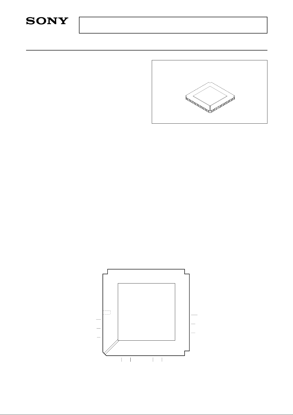
CXA1166K
68 pin LCC (Ceramic)
Structure
Bipolar silicon monolithic IC
Features
• Differential linearity error: ±0.5 LSB or less
• Integral linearity error: ±0.5 LSB or less
• Built-in integral linearity compensation circuit
• Ultrahigh-speed operation with maximum conver-
sion rate of 250 MSPS
• Low input capacitance: 18pF
• Wide analog input bandwidth: 250MHz (full-scale
input, standard)
• Single power supply: –5.2V
• Low power consumption: 1.4W (Typ.)
• Low error rate
• Good temperature characteristics
• Capable of driving 50Ω loads
Pin Configuration (Top View)
Pins without name are NC pins (not connected internally).
EE
IN1
IN1
AGND
V
V
AGND
AV
VRT
VRTS
AVEE
AVEE
LINV
OR
OR
D0
D0
D1
D1
DV
AV
60
59
58
61
62
EE
63
64
65
66
67
68
1
2
3
4
5
6
7
EE
8
9
57
10
11
12
13
D2
D2
56
14
D3
55
15
D3
AGND
54
53
16
17
DGND2
DGND2
Applications
• Digital oscilloscopes
• Other apparatus requiring ultrahigh-speed A/D
conversion
RM
IN2
IN2
V
52
18
DGND1
AGND
V
51
50
19
20
D4
D4
V
49
21
D5
AGND
48
47
22
23
D5
45
44
46
24
AGND
43
EE
AV
42
41
VRB
40
VRBS
39
AVEE
38
AVEE
37
36
CLK
35
CLK
34
MINV
33
D7
32
D7
31
D6
30
D6
29
EE
DV
28
27
25
26
Sony reserves the right to change products and specifications without prior notice. This information does not convey any license by
any implication or otherwise under any patents or other right. Application circuits shown, if any, are typical examples illustrating the
operation of the devices. Sony cannot assume responsibility for any problems arising out of the use of these circuits.
– 1 –
E90406-ST

Absolute Maximum Ratings (Ta = 25°C)
• Supply voltage AVEE, DVEE –7 to +0.5 V
• Analog input voltage VIN –2.7 to +0.5 V
• Reference input voltage VRT, VRB, VRM –2.7 to +0.5 V
| VRT – VRB | 2.5 V
• Digital input voltage MINV, LINV, CLK, CLK –4 to +0.5 V
| CLK – CLK | 2.7 V
• VRM pin input current IVRM –3 to +3 mA
• Digital output current ID0 to ID7, IOR, ID0 to ID7, IOR –30 to 0 mA
• Storage temperature Tstg –65 to +150 °C
Operating Conditions Min. Typ. Max. Unit
• Supply voltage AVEE, DVEE –5.5 –5.2 –4.95 V
AVEE – DVEE –0.05 0 0.05 V
AGND – DGND –0.05 0 0.05 V
• Reference input voltage VRT –0.1 0 0.1 V
VRB –2.2 –2.0 –1.8 V
• Analog input voltage VIN VRB VRT
• Operating temperature Tc –20 100 °C
CXA1166K
– 2 –
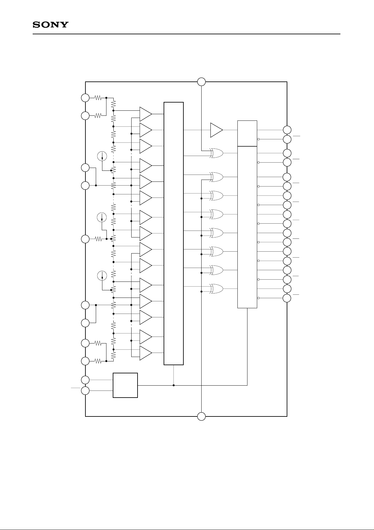
Block Diagram
VRTS
CXA1166K
MINV
33
r1
RT
V
64
r2
65
r/2
r
Comparator
0
VIN1
VRM
VIN2
VRBS
VRB
55
52
50
54
49
39
40
2
3
31
32
29
30
21
22
19
20
14
15
12
13
6
7
4
5
OR
OR
D7 (MSB)
D7
D6
D6
D5
D5
D4
D4
D3
D3
D2
D2
D1
D1
D0 (LSB)
D0
63
1
2
•
•
•
r
r
r
64
r
65
126
127
128
•
•
•
OUTPUT
ENCODE LOGIC
r
r
r3
r
r
129
191
•
•
•
r
r
192
r
193
254
255
•
•
•
r
r
4
5
r
r
r/2
CLK
CLK
35
34
CLOCK
DRIVER
1
LINV
– 3 –
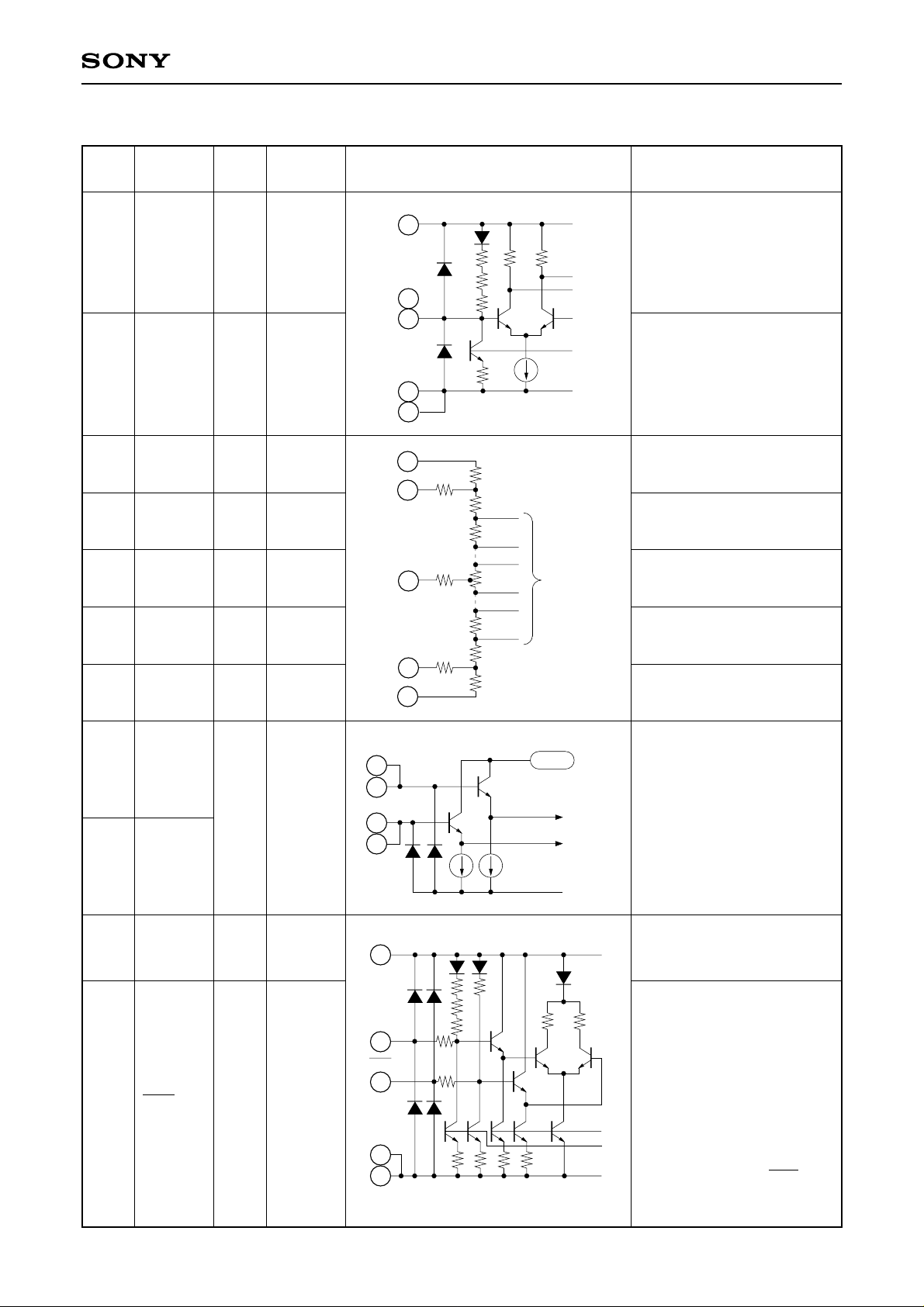
Pin Description
CXA1166K
Pin
No.
Symbol I/O
Standard
voltage level
1 LINV I ECL
33 MINV I ECL
64 VRT I0V
65 VRTS O0V
52 VRM IVRB/2
VRT
VRTS
VRM
Equivalent circuit Description
DGND1
18
LINV
1
or
33
MINV
r
r
r
–1.3V
Polarity selection other than
MSB and overrange.
(Refer to the table of input
voltage vs. Digital output)
Low level is maintained with
left open.
Polarity selection for MSB
(Refer to the table of input
DV
64
28
65
25
EE
8
r
r
r⁄2
r
r
1
To
Comparator
r2
r3
voltage vs. Digital output)
Low level is maintained with
left open.
Reference voltage
(Top) (0V typ.)
Reference voltage sense
(Top)
Reference voltage mid-point.
Can be used for linearity
compensation.
39 VRBS O –2V
VRBS
39
40 VRB I –2V Reference voltage (Bottom)
54
VIN1
55
VRTS
I
to
VRBS
49
VIN2
50
35
34
CLK
CLK
I
I
ECL
ECL
VRB
VIN1
54
55
49
50
VIN2
DGND1
18
CLK
35
CLK
34
40
r
r
4
r ⁄2
r5
43, 48, 51, 53, 56, 61
AGND
To Comp
0 to 127
128 to 255
r
r
r
r
Reference voltage sense
(Bottom)
Analog input.
Pins 49, 50 and Pins 54, 55
should be connected
externally.
CLK input
Complementary CLK input.
ECL threshold potential
(–1.3V) is maintained with
left open.
The complementary input is
recommended for stable
operation at high speed
DV
28
EE
8
r r
though the operation only
with the CLK input is
possible when the CLK
input is left open.
– 4 –
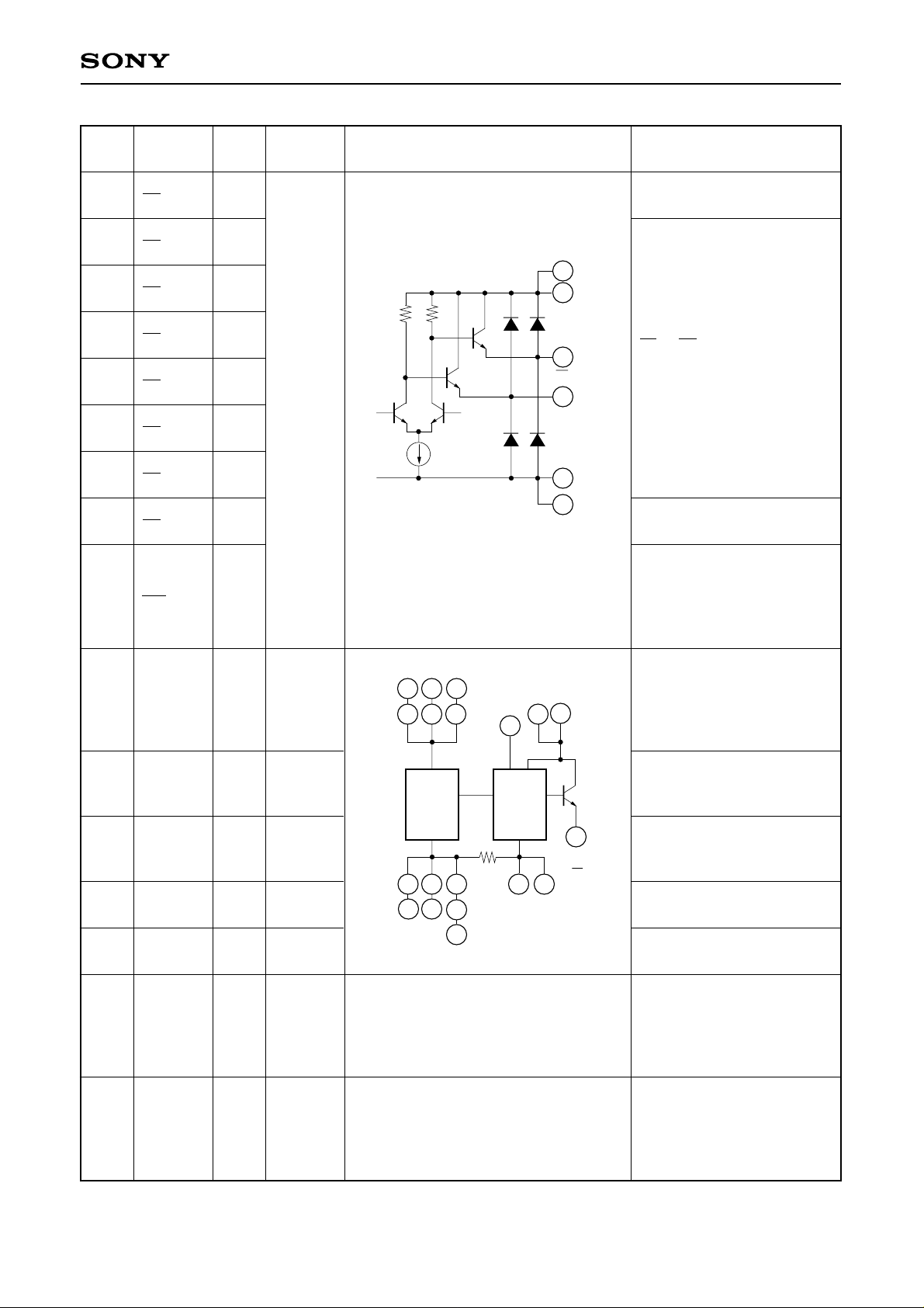
CXA1166K
Pin
No.
31
32
29
30
21
22
19
20
14
15
12
13
6
7
4
5
2
3
Symbol I/O
D7
D7
D6
D6
D5
D5
D4
D4
D3
D3
D2
D2
D1
D1
D0
D0
OR
OR
O
O
O
O
O
O
O
O
O
Standard
voltage level
ECL
Equivalent circuit Description
MSB and complementary
MSB output
DGND2
16
17
D1 to D6: Output
D1 to D6: Complementary
output
LSB and complementary
DV
EE
Di
Di
8
28
LSB output
Overrange output;
Low level for overrange.
Overrange complementary
output;
High level for overrange.
37, 38,
42, 58,
62,66,
AVEE∗
67
43, 48,
51,53,
AGND∗
56,61
8
DVEE∗
28
18 DGND1
16
DGND2∗
17
41, 44,
45, 46,
47, 57,
NC
59, 60,
63
9, 10,
11, 23,
24, 25,
NC —
26, 27,
36, 68
–5.2V
0V
–5.2V
0V
0V
—
AGND
61
43
Internal
Analog
Circuit
42
62
AVEE
48
51
37
38
53
56
58
66
67
DGND1
4 to 6Ω
DGND2
18
Internal
Digital
Circuit
8
DV
16
EE
28
17
Analog supply.
Internally connected with
DVEE (resistance: 4 to 6Ω).
Analog ground.
Separated from DGND.
Digital supply.
Di
Di
Internally connected with
AVEE (resistance: 4 to 6Ω).
Digital ground
Digital ground for output
drive
No connected.
It is recommended to connect
these pins to AGND.
No connected.
It is recommended to connect
these pins to DGND.
∗ For stable operation, all of these pins must be connected on the corresponding PCB pattern.
– 5 –
CXA1166K
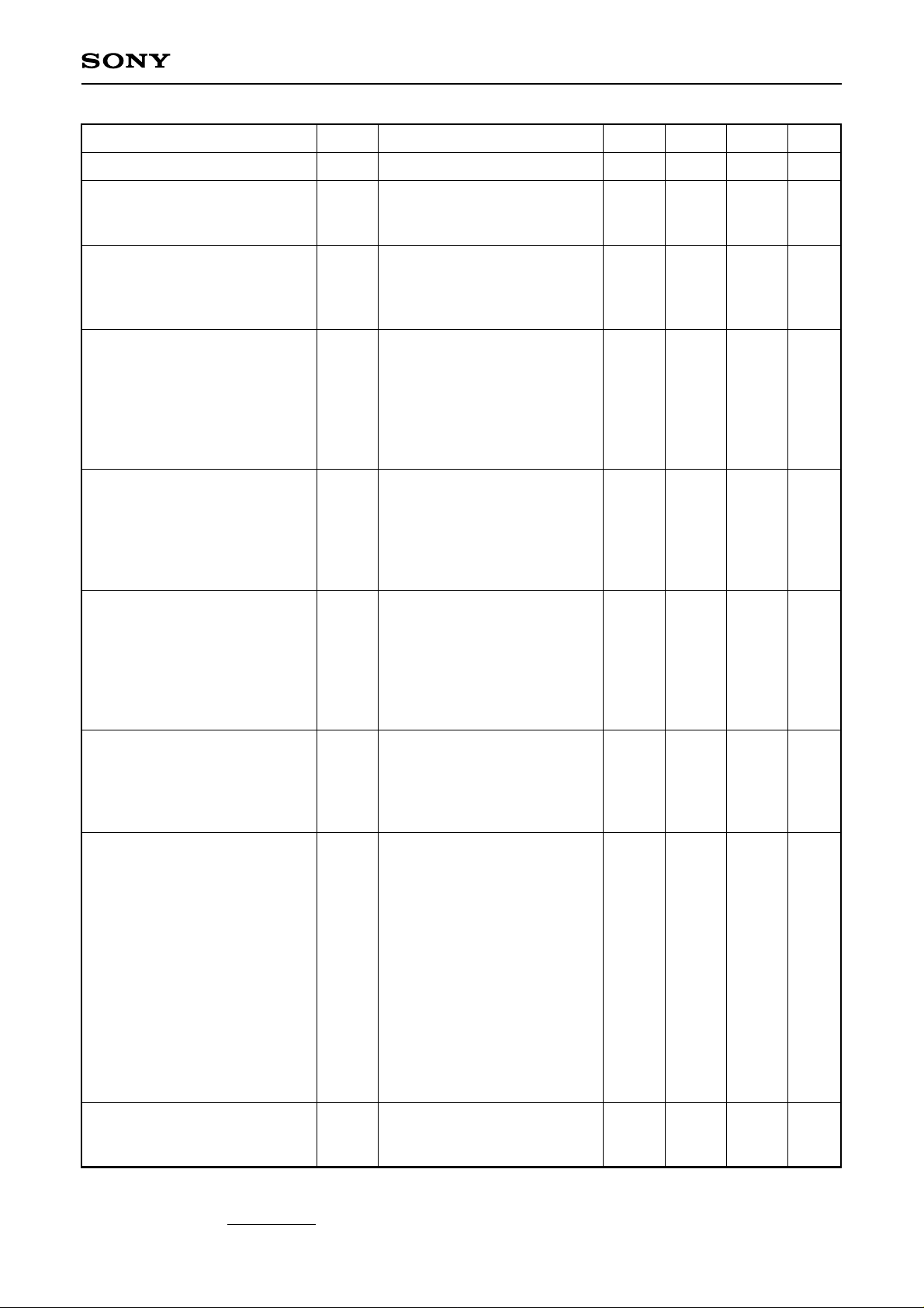
Electrical Characteristics (AVEE = DVEE = –5.2V, VRT, VRTS = 0V, VRB, VRBS = –2V, Ta = 25°C)
Item
Resolution
DC characteristics
Integral linearity error
Differential linearity error
Analog input
Analog input capacitance
Analog input resistance
Input bias current
Reference inputs
Reference resistance
Residual resistance∗1r1
Digital inputs
Logic High level
Logic Low level
Logic High current
Logic Low current
Input capacitance
Symbol Condition Min. Typ. Max.
8
EIL
EDL
CIN
RIN
IIN
RREF
r1
r2
r3
r4
r5
r2
r3
r4
r5
VIH
VIL
IIH
IIL
VIN = –1V + 0.07Vrms
VIN = –1V
VIN = –1V
VIH = –0.8V
VIL = –1.6V
50
20
83
0.1
300
0.5
300
0.1
–1.13
0
–50
18
120
125
0.6
500
2.0
500
0.6
4
±0.5
±0.5
450
182
2.0
700
5.0
700
2.0
–1.50
70
50
Unit
bits
LSB
LSB
pF
kΩ
µA
Ω
Ω
Ω
Ω
Ω
Ω
V
V
µA
µA
pF
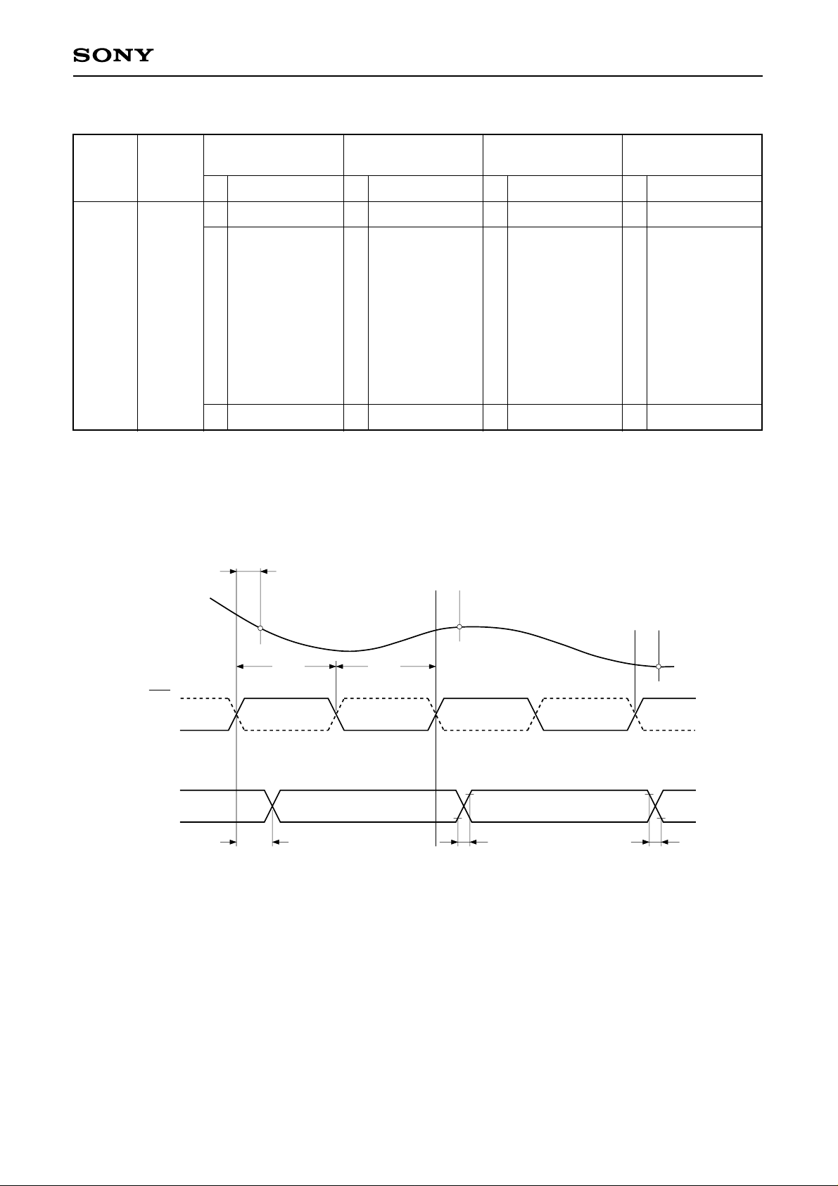
Switching characteristics
Maximum conversion rate
Aperture jitter
Sampling delay
Output delay
Clock High pulse width
Clock Low pulse width
Digital output
Logic High level
Logic Low level
Output rise time
Output fall time
Dynamic characteristics
Input bandwidth
SNR
Error rate
Differential gain error
Differential phase error
Fc
Taj
Tds
Tdo
TPW1
TPW0
VOH
VOL
Tr
Tf
SNR
DG
DP
RL = 50Ω to –2V
TPW1 + TPW0 = 4.0ns
}
RL = 50Ω to –2V
RL = 50Ω to –2V
RL = 50Ω to –2V
RL = 50Ω to –2V
VIN=2Vp-p
Input = 1kHz, FS
{
Clock = 250MHz
Input = 62.499MHz, FS
{
Clock = 250MHz
Input = 49.999MHz, FS
Error > 16LSB
{
Clock = 200MHz
Input = 62.499MHz, FS
Error > 16LSB
{
Clock = 250MHz
NTSC 40IRE mod.
}
ramp, Fc = 250MSPS
250
0.4
1.8
1.8
1.8
–1.00
200
44
30
1.4
2.5
0.6
0.6
10
1.0
0.5
9
46
35
MSPS
ps
2.4
3.2
–1.60
1.5
1.5
10
–8
10
ns
ns
ns
ns
V
V
ns
ns
MHz
dB
dB
TPS∗
TPS∗
%
deg
2
2
–9
–6
Power supply
Supply current
Power consumption∗
∗1 See Block Diagram.
∗2 TPS: Times Per Sample
∗3 Pd = IEE • VEE +
3
(VRT – VRB)
RREF
IEE
Pd
2
– 6 –
–360
–270
1.4
1.9
mA
W
Input Voltage vs. Digital Output
CXA1166K
VIN∗
0V
Step
0
1
MINV 1
LINV 1
D7 D0 D7 D0 D7 D0 D7 D0
OR
0 0 0 …… 0 0
0
0 0 0 …… 0 0
1
0 0 0 …… 0 1
1
OR
0
1
1
0
1
1 0 0 …… 0 0
1 0 0 …… 0 0
1 0 0 …… 0 1
:
:
–1V
–2V
127
128
254
255
0 1 1 …… 1 1
1
1 0 0 …… 0 0
1
:
:
1 1 1 …… 1 0
1
1 1 1 …… 1 1
1
1 1 1 …… 1 1
1
1 1 1 …… 1 1
1
0 0 0 …… 0 0
1
:
:
:
:
0 1 1 …… 1 0
1
0 1 1 …… 1 1
1
0 1 1 …… 1 1
1
∗ VRT = VRTS =0V, VRM = –1V or Open, VRB = VRBS = –2V
Timing Diagram
1
0
OR
0 1 1 …… 1 1
0
0 1 1 …… 1 1
1
0 1 1 …… 1 0
1
:
:
1
1
:
:
:
:
1
1
1
:
:
0 0 0 …… 0 0
1 1 1 …… 1 1
:
:
1 0 0 …… 0 1
1 0 0 …… 0 0
1 0 0 …… 0 0
OR
0
1
1
1
1
:
:
1
1
1
0
0
1 1 1 …… 1 1
1 1 1 …… 1 1
1 1 1 …… 1 0
:
:
1 0 0 …… 0 0
0 1 1 …… 1 1
:
:
0 0 0 …… 0 1
0 0 0 …… 0 0
0 0 0 …… 0 0
Analog input
CLK
CLK
Digital output
Tds
Td
N
Tpw0Tpw1
20%
N + 1
80%
Tr Tf
NN – 1
80%
N + 2
N + 1
20%
– 7 –
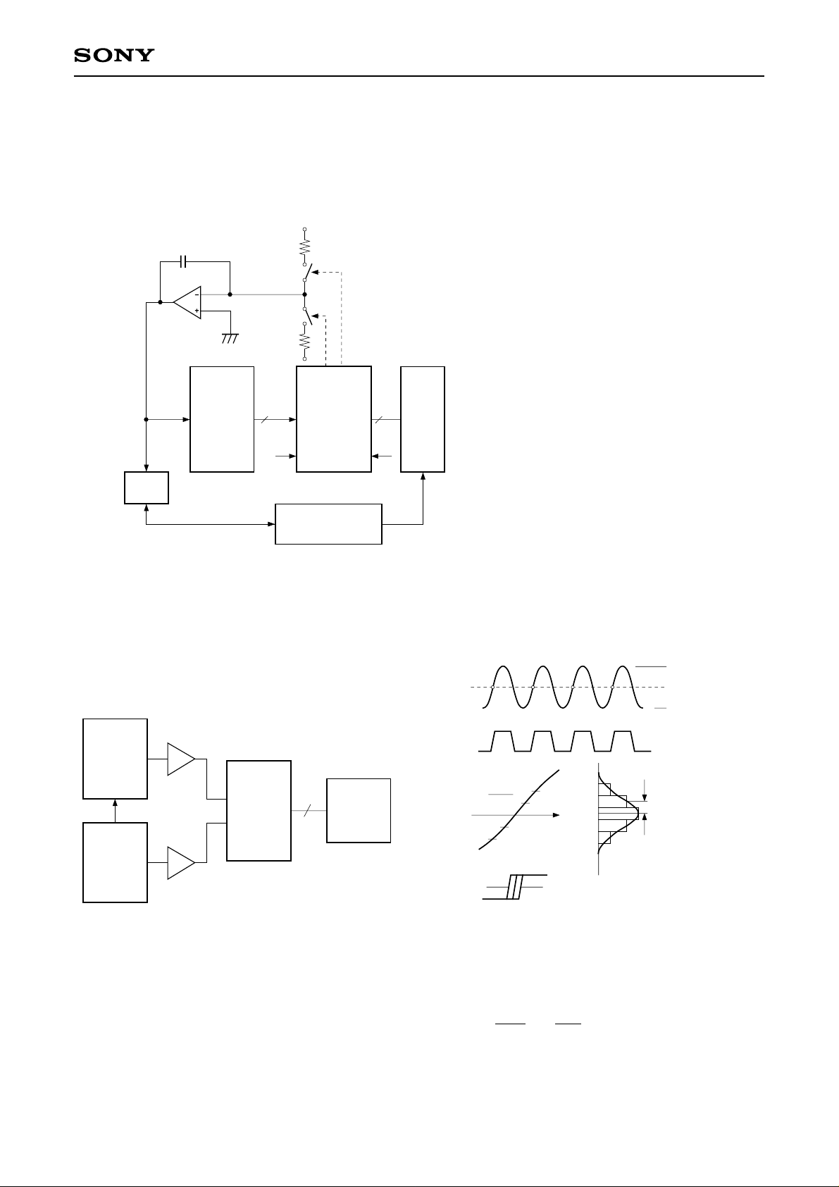
Electrical Characteristics Measurement Circuit
Integral Linearity Error Measurement Circuit
Differential Linearity Error Measurement Circuit
+ V
S2
S1:ON when A<B
S2: ON when A>B
S1
– V
A<B A>B
Comparator
DVM
V
IN
DUT
CXA1166K
8 8
A8
to
A1
A0
Controller
B8
to
B1
B0
“1 ”“0 ”
CXA1166K
Buffer
000•••0 0
to
111•••1 0
Sampling Delay Measurement circuit
Aperture Jitter Measurement circuit
60MHz
Amp
OSC1
φ:Variable
V
OSC2
60MHz
IN
fr
CLK
ECL
Buffer
CXA1166K
8
Logic
Analizer
1024
samples
Aperture Jitter Measurement Method
0V
VIN
CLK
∆
υ
∆ t
IN
V
CLK
When the distribution of the output codes is σ (unit: LSB) If
the maximum slew rate point is sampled with the clock signal
having the same frequency as that of the analog input signal,
Aperture jitter (Taj) is defined as follows:
Taj = σ/ = σ/ ( )
∆υ
∆t
129
128
t
127
126
125
Sampling timing fluctuation
( = aperture jitter)
256
× 2πf
2
–1V
–2V
σ (LSB)
– 8 –
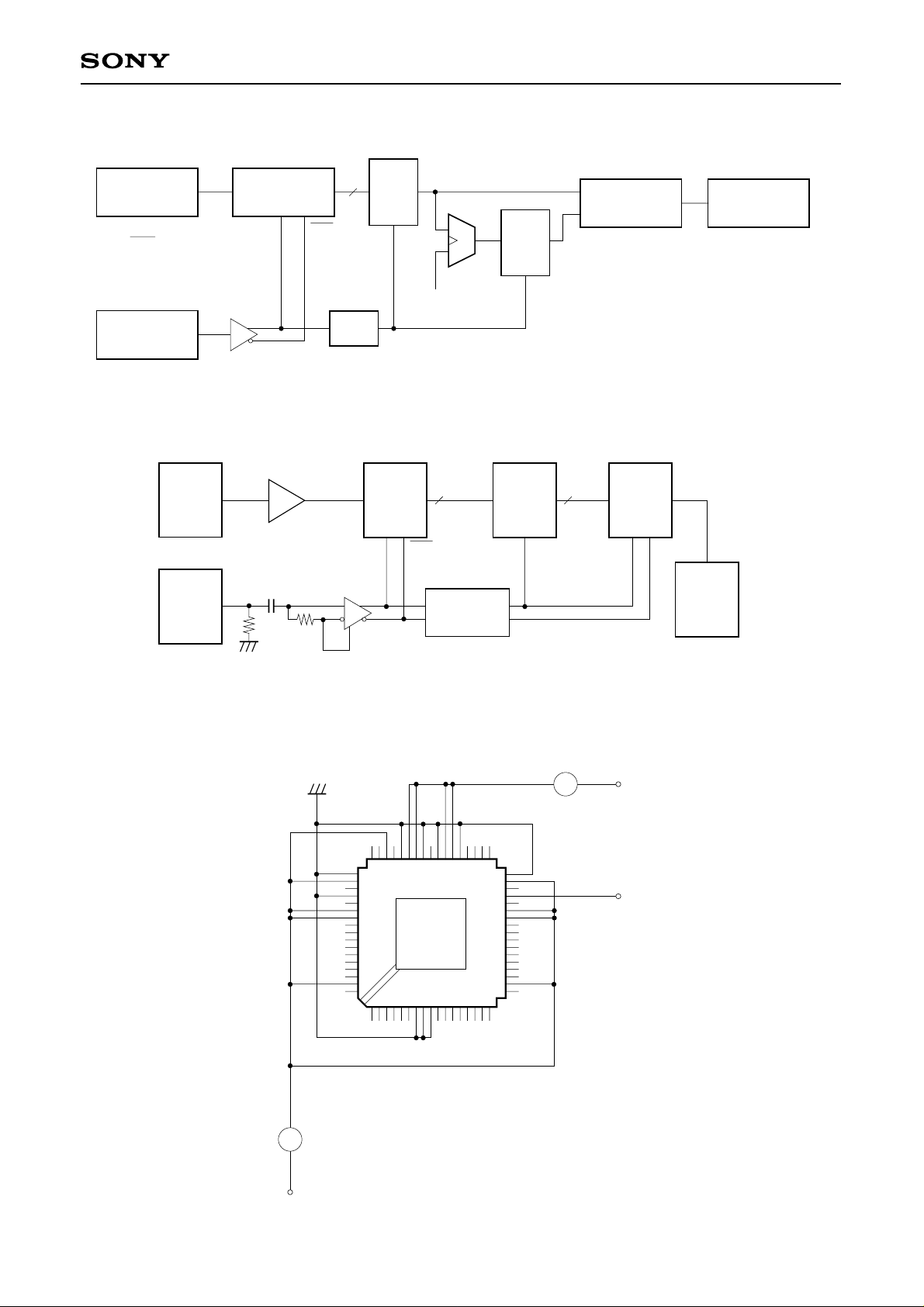
Error Rate Measurement Circuit
CXA1166K
Signal
Source
fCLK
– 1kHz
4
2Vp – p Sine Wave
Signal
Source
fCLK
Vin
CXA1166K
CLK CLK
8
1⁄16
ECL
Latch
Differential Gain Error Measurement Circuit
Differential Phase Error Measurement Circuit
NTSC
Signal
Source
SG (CW)
Amp
50
DUT
CXA1166K
CLK CLK
VBB
+
DAT A 16
8 8
Decimator
ECL
Latch
ECL
Latch
A
B
Comparator
A<B
(CX20202A – 1)
10bit
D⁄A
Pulse
Counter
Vector
Scope
Power Supply Current Measurement Circuit
Analog Input Bias Current Measurement Circuit
60
61
1
CXA1166K
9
10
A
EE
I
44
26
43
27
IIN
A
– 1V
– 2V
– 5.2V
– 9 –
 Loading...