

Sony CPD-E43, TRINITRON CPD-E430 Service Manual
CHASSIS
SERVICE MANUAL
SPECIFICATIONS
CPD-E430
CRV
AEP Model
Chassis No. SCC-L42G-A
TRINITRON® COLOR COMPUTER DISPLAY
CRT
0.24 mm aperture grille pitch, 90-degree deflection, FD Tri n itron
19 inches measured diagonally
Viewable image size
Approx. 365
× 274 mm (w/h) (14
3
/8 × 10 7/8 inches)
18.0" viewing image
Resolution (H:Horizontal, V:Vertical)
Maximum: H: 1920 dot s, V: 1440 lines
Recommended: H: 1280 dots, V: 1024 lines
Input signal levels
Video signal: Analog RGB: 0.700 Vp- p (posi ti ve ), 7 5
Ω
SYNC signal: H/V separate or composite sync:
TTL 2 k
Ω, Polarity free
Sync on Green: 0. 3 Vp -p (negative)
Standard imag e a r ea
Approx. 352
× 264 mm
(13
7
/8 × 10 1/2 inches)
Deflection frequency (H:Horizontal, V:Vertical)
H: 30 to 96 kHz, V: 48 to 170 H z
AC input voltage/current
100 to 240 V, 50 – 60 Hz, 2.0 – 1.0 A
Power Consumption
Approx. 135 W
Operating temperature
10 ºC to 40 ºC
Dimensions Approx. 451
× 471 × 461 mm (w/h/d)
(17
7
/8 × 18 5/8 × 18 1/4 inches)
Mass Approx. 25.5 kg (56 lb 3 oz)
Plug and Play DDC2B/DDC2Bi
GTF
CPD-E430 (E) 2
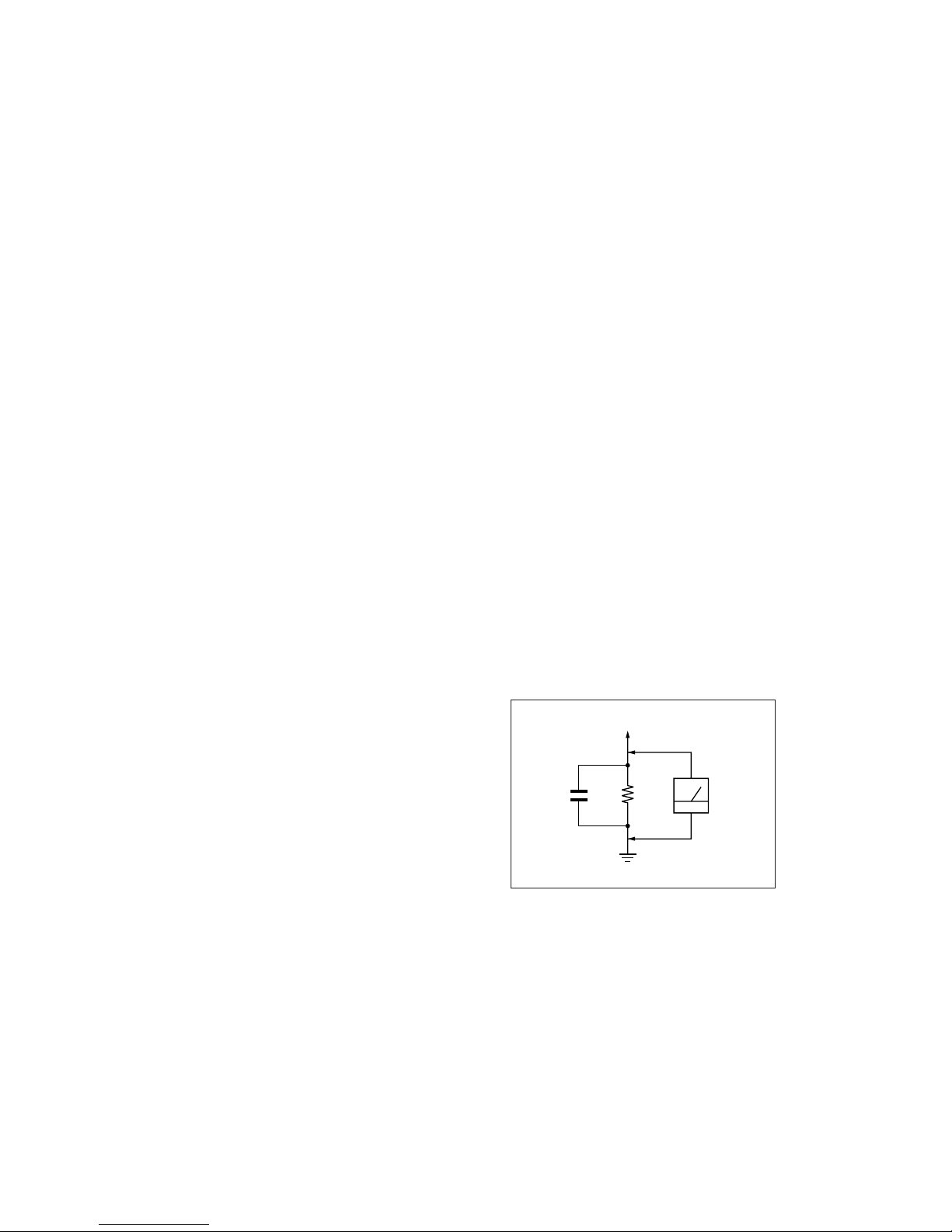
LEAKAGE TEST
The AC leakage from any exposed metal part to earth ground and from all
exposed metal parts to any exposed metal part having a return to chassis,
must not exceed 0.5 mA (500 microamperes).
Leakage current can be measured by any one of three methods.
1. A commercial leakage tester, such as the Simpson 229 or RCA WT540A. Follow the manufacturers’ instructions to use these instruments.
2. A battery-operated AC milliammeter. The Data Precision 245 digital
multimeter is suitable for this job.
3. Measuring the voltage drop across a resistor by means of a VOM or battery-operated AC voltmeter. The “limit” indication is 0.75 V, so analog
meters must have an accurate low-voltage scale. The Simpson 250 and
Sanwa SH-63Trd are examples of a passive VOMs that are suitable.
Nearly all battery operated digital multimeters that have a 2 V AC range
are suitable. (See Fig. A)
After correcting the original service problem, perform the following safety
checks before releasing the set to the customer:
1. Check the area of your repair for unsoldered or poorly-soldered connections. Check the entire board surface for solder splashes and bridges.
2. Check the interboard wiring to ensure that no wires are “pinched” or contact high-wattage resistors.
3. Check that all control knobs, shields, covers, ground straps, and mounting hardware have been replaced. Be absolutely certain that you have
replaced all the insulators.
4. Look for unauthorized replacement parts, particularly transistors, that
were installed during a previous repair. Point them out to the customer
and recommend their replacement.
5. Look for parts which, though functioning, show obvious signs of deterioration. Point them out to the customer and recommend their replacement.
6. Check the line cords for cracks and abrasion. Recommend the replacement of any such line cord to the customer.
7. Check the B+ and HV to see if they are specified values. Make sure your
instruments are accurate; be suspicious of your HV meter if sets always
have low HV.
8. Check the antenna terminals, metal trim, “metallized” knobs, screws, and
all other exposed metal parts for AC Leakage. Check leakage as described below.
Fig. A. Using an AC voltmeter to check AC leakage.
1.5 k
Ω
0.15 µF
AC
Voltmeter
(0.75 V)
To Exposed Metal
Parts on Set
Earth Ground
SAFETY CHECK-OUT

CPD-E430 (E) 3
WARNING!!
NEVER TURN ON THE POWER IN A CONDITION IN WHICH THE
DEGAUSS COIL HAS BEEN REMOVED.
SAFETY-RELATED COMPONENT WARNING!!
COMPONENTS IDENTIFIED BY SHADING AND MARK ¡ ON THE
SCHEMATIC DIAGRAMS, EXPLODED VIEWS AND IN THE
PARTS LIST ARE CRITICAL FOR SAFE OPERATION. REPLACE
THESE COMPONENTS WITH SONY PARTS WHOSE PART NUMBERS APPEAR AS SHOWN IN THIS MANUAL OR IN SUPPLEMENTS PUBLISHED BY SONY. CIRCUIT ADJUSTMENTS THAT
ARE CRITICAL FOR SAFE OPERATION ARE IDENTIFIED IN THIS
MANUAL. FOLLOW THESE PROCEDURES WHENEVER CRITICAL COMPONENTS ARE REPLACED OR IMPROPER OPERATION IS SUSPECTED.

CPD-E430 (E) 4
POWER SAVING FUNCTION
This monitor meets the power-saving guide li ne s set by VESA, TC O’99,
and
E
NERGY STAR. If no signal is input to the monitor from your
computer, the monitor will automatically reduce power consumption as
shown below.
*
1
When your computer enters power saving mode, NO SIGNAL appears
on the screen. After a few seconds, the monito r ent ers power savi ng
mode.
*
2
“Deep sleep” is power saving mode defined by the Environmental
Protection Agency.
Power mode Power consumption ! (power)
indicator
normal operation
≤ 135 W green
active off*
1
(deep sleep)*
2
≤ 3 W orange
CPD-E430 (E) 5
DIAGNOSIS
Failure
+B failure
Horizontal / Vertical Deflection
failure, Thermal protector
ABL protector
HV failure
Aging / Self Test
Out of scan range
Power LED
Amber → Off
(0.5 sec) (0.5 sec)
Amber → Off
(1.5 sec) (0.5 sec)
Amber → Off
(0.5 sec) (1.5 sec)
Amber → Off → Amber → Off
(0.25 sec) (0.25 sec) (0.25 sec) (1.25 sec)
Amber → Off → Green → Off
(0.5 sec) (0.5 sec) (0.5 sec) (0.5 sec)
Green (OSD indication)
Aging Mode (Video Aging) : During Power Save, press MENU button for longer than 2 second.
Self Test (OSD Color Bar) : During Power Save, push up Control button for longer than 2 second.
Reliability Check Mode : During Power Save, push down Control button for longer than 2 second.
CPD-E430 (E) 6
TIMING SPECIFICATION
MODE AT PRODUCTION
MODE 1 MODE 2 MODE 3
RESOLUTION
640 X 480 1280 X 1024 1600 X 1200
CLOCK
25.175 MHz 157.500 MHz 202.500 MHz
HORIZONTAL
H-FREQ
31.469 kHz 91.146 kHz 93.750 kHz
usec usec usec
H. TOTAL
31.778 10.971 10.667
H. BLK
6.356 2.844 2.765
H. FP
0.636 0.406 0.316
H. SYNC
3.813 1.016 0.948
H. BP
1.907 1.422 1.501
H. ACTIV
25.422 8.127 7.901
VERTICAL
V. FREQ (HZ)
59.940 Hz 85.024 Hz 75.000 Hz
lines lines lines
V. TOTAL
525 1072 1250
V. BLK
45 48 50
V. FP
10 1 1
V. SYNC
23 3
V. BP
33 44 46
V. ACTIV
480 1024 1200
SYNC
INT(G)
NO NO NO
EXT (H/V) /POLARITY
YES N/N YES P/P YES P/P
EXT (CS) /POLARITY
NO NO NO
INT/NON INT
NON INT NON INT NON INT
2001.6.15 VER.

CPD-E430 (E) 7
TABLE OF CONTENTS
Section Title Page Section Title Page
1. DISASSEMBLY
1-1. Cabinet Removal ............................................... 1-1
1-2. A Board (C BLOCK) Removal ......................... 1-2
1-3. A Board Removal .............................................. 1-3
1-4. Bezel Assembly, H1 Board Removal ............... 1-4
1-5. D Board Removal .............................................. 1-5
1-6. Service Position .................................................. 1-6
1-7. Picture Tube Removal........................................ 1-7
1-8. Harness Location ............................................... 1-9
2. SAFETY RELATED ADJUSTMENT
............. 2-1
3. ADJUSTMENTS
..................................................... 3-1
4. DIAGRAMS
4-1. Block Diagrams .................................................. 4-1
4-2. Frame Schematic Diagram ................................. 4-4
4-3. Circuit Boards Location ..................................... 4-5
4-4. Schematic Diagrams and Printed Wiring
Boards ................................................................. 4-6
(1) Schematic Diagram of A Board ........................ 4-8
(3) Schematic Diagram of DA Board ..................... 4-14
(4) Schematic Diagram of H1 Board....................... 4-16
(5) Schematic Diagram of N Board 4-18
4-5. Semiconductors ................................................. 4-20
5. EXPLODED VIEWS
5-1. Chassis ............................................................... 5-2
5-2. Picture Tube ...................................................... 5-3
5-3. Packing Materials ............................................... 5-4
6. ELECTRICAL PARTS LIST
............................ 6-1
(2) Schematic Diagrams of
D (a, b, c) Board ........................................ 4-10
........................
CPD-E430 (E) 1-1
SECTION 1
DISASSEMBLY
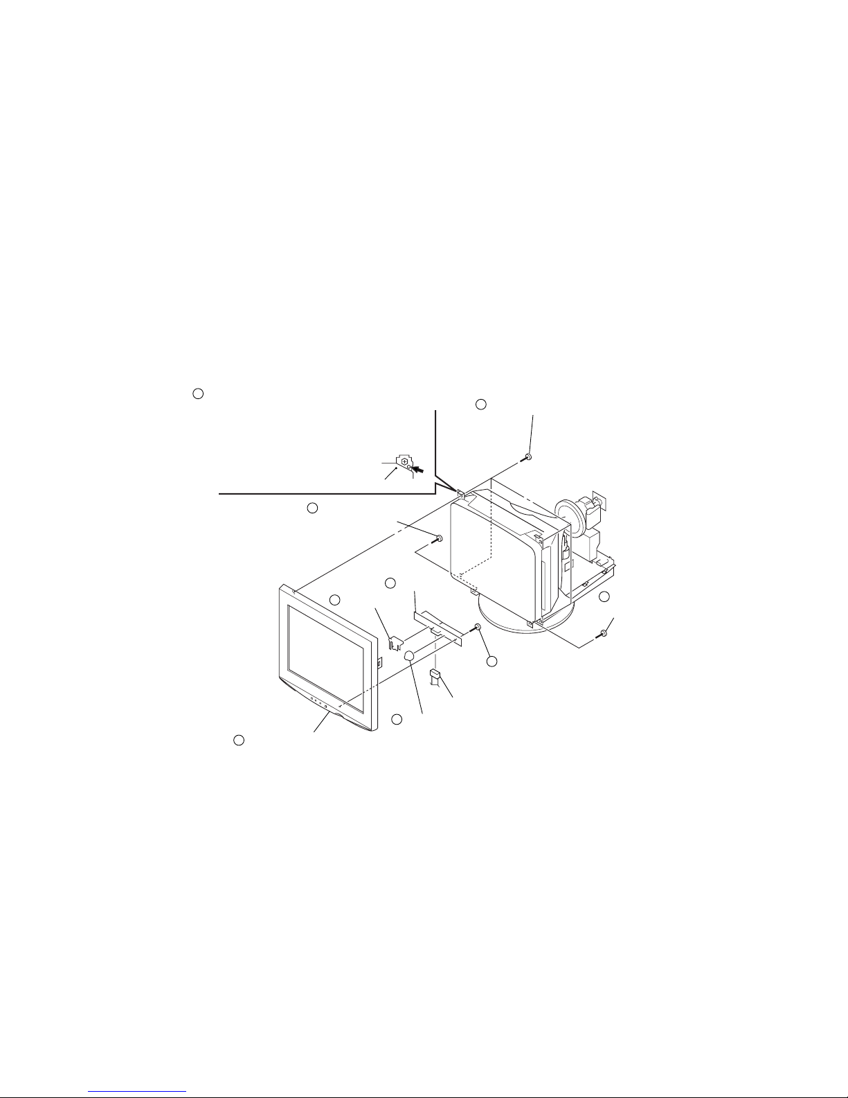
1-1. CABINET REMOVAL
1
B
A
C
Two screws
(+BVTP 4 x 16)
6
Slide the EMI shield in the direction
of arrow C and remove four claws.
7
EMI shield
4
Two screws
(+BVTT 3 x 8)
5
Six screws
(+BVTT 4 x 8)
2
Two claws
3
Push the upper side of the cabinet
inthe direction of arrow A, disconnect claws
then remove the cabinet
lifting it up in the direction of arrow B.
Bezel assembly
Bezel assembly
EMI shield
Cabinet
Cabinet
Push in the tip of a screwdriver
about 10mm to unlock the claw.
CPD-E430 (E) 1-2
1-2. A BOARD (C BLOCK) REMOVAL
1
A board
CN315
CN318
GND
GND
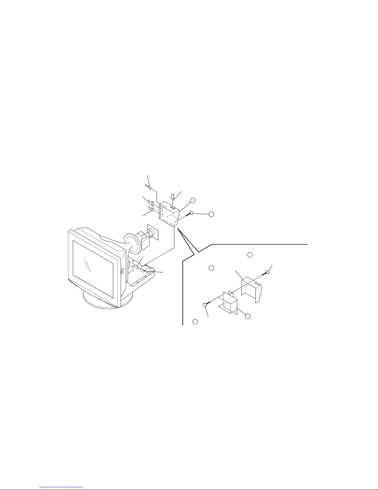
CPD-E430 (E) 1-3
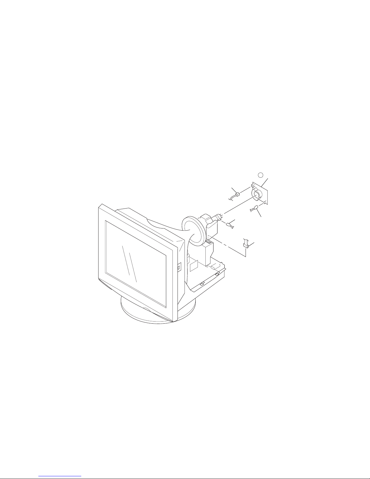
1-3. A BOARD REMOVAL
Two screws
(+BVTT 4 x 8)
Video block assembly
3
Four screws
(+BVTT 3 x 8)
Screw
(+BVTP 3 X 10)
Video case
CN315
CN313
CN304
CN604
CN1102
1
4
6
A board
5
GND
2
CPD-E430 (E) 1-4
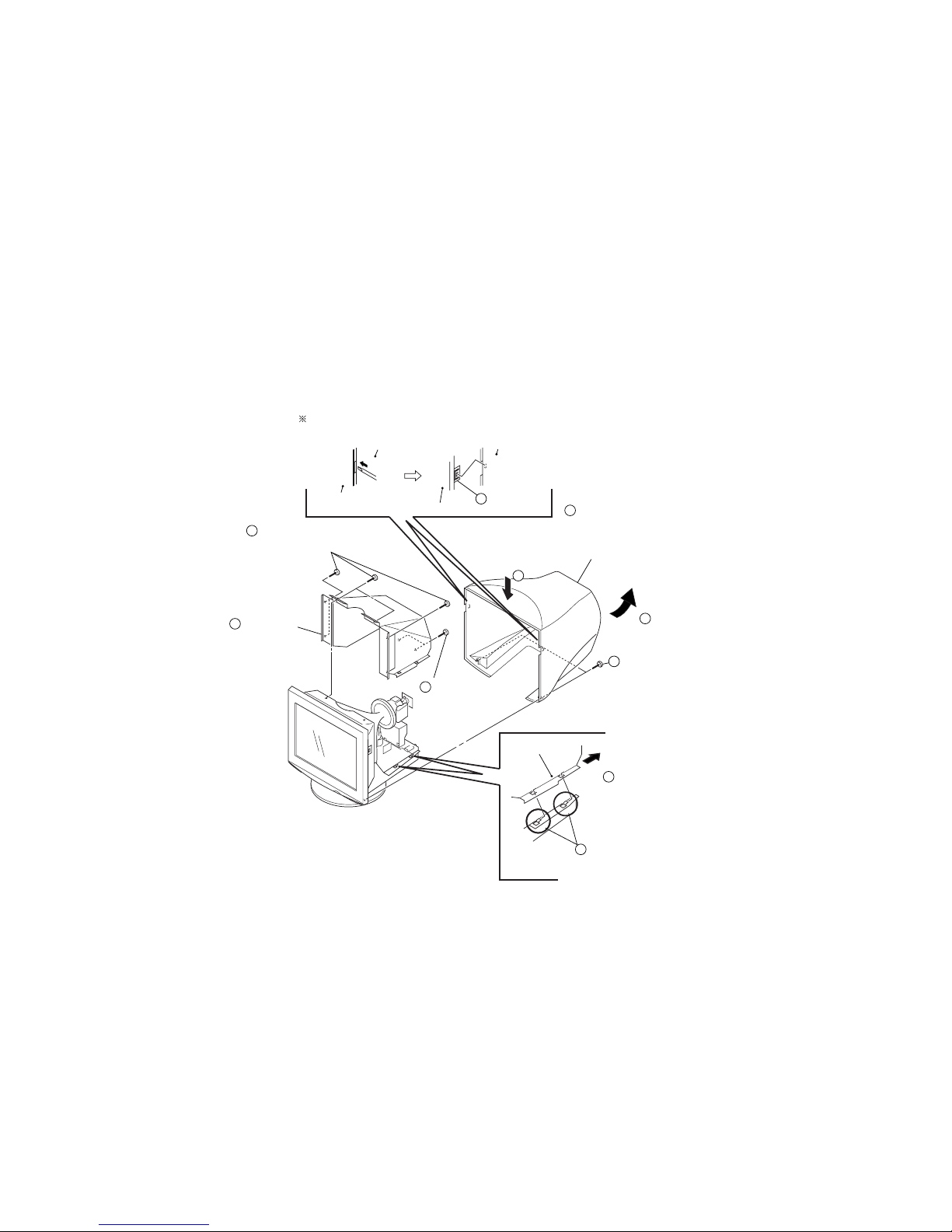
1-4. BEZEL ASSEMBLY, H1 BOARD REMOVAL
2
1
Four tapping screws (5)
5
Bezel assembly
3
Screw
(+BVTP 4 x 16)
4
Screw
(+BVTP 4 x 16)
Three screws
(+BVTP 3 x 10)
9
H1 board
8
Menu button
CN1400
Picture tube shield
Before removing the bezel assembly, secure
the picture tube by attaching two screws to
the picture tube shield at the positions shown
with an arrow (diagonal two places) to prevent
the picture tube from falling.
(Use the screws +BVTT 4 x 8 that fix EMI shield.)
6
Joy stick
7
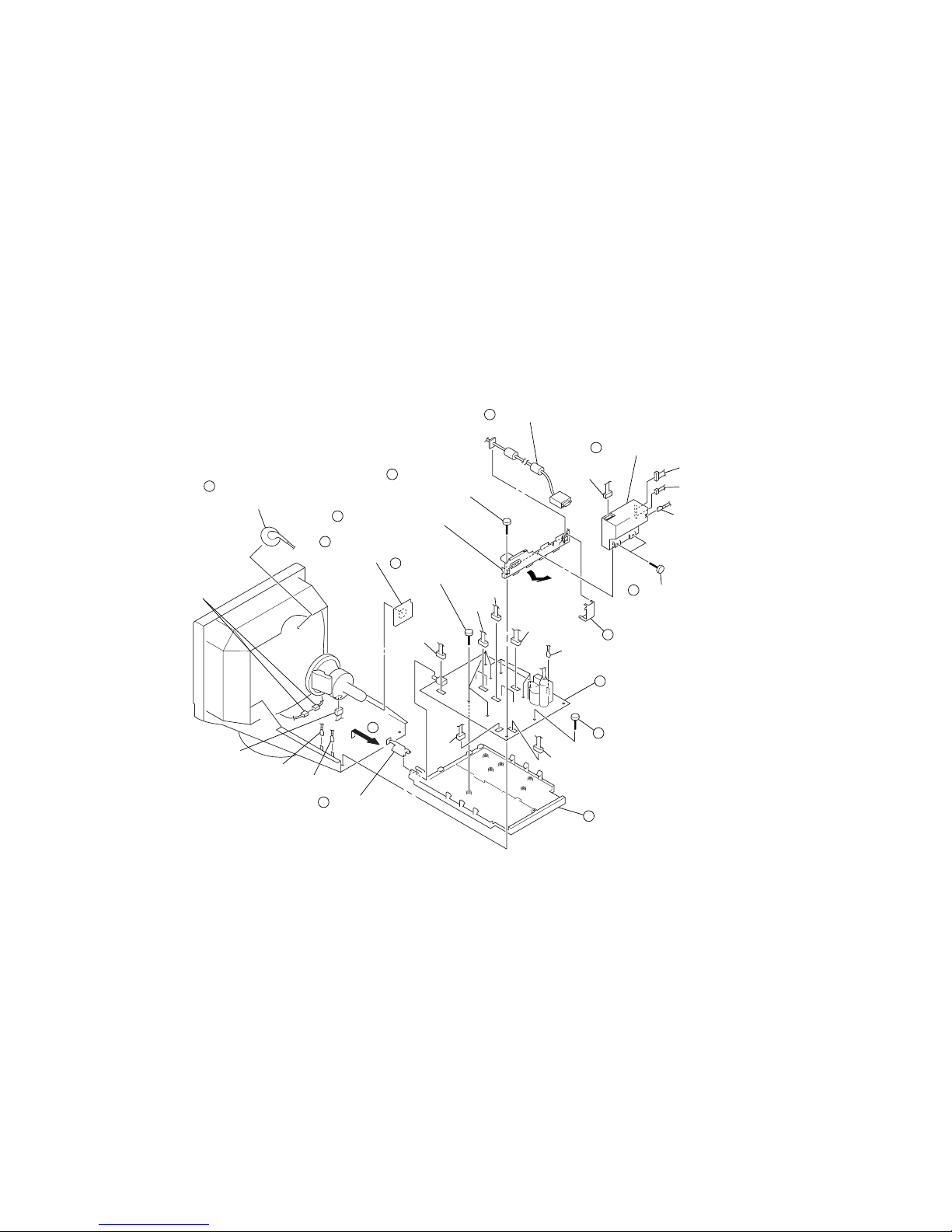
CPD-E430 (E) 1-5
1-5. D BOARD REMOVAL
2
A board
(C block)
1
Anode cap
(Refer to 1-8)
3
Two screws
(+BVTT 4 x 8)
7
Two screws
(+BVTT 3 x 8)
Pig tail cover
14
D board
13
PWB bracket
4
Video block assembly
6
Cable with connector
8
Rear plate assembly
Screw (+BVTT 3 x 8)
11
Seven screws
(+BVTP 3 x 10)
12
9
Extension bar
CN315
CN313
CN304
GND
CN600
CN601
CN1103
CN1602
Connector (2P)
CN501
CN701
GND
GND
GND
CN
10
5
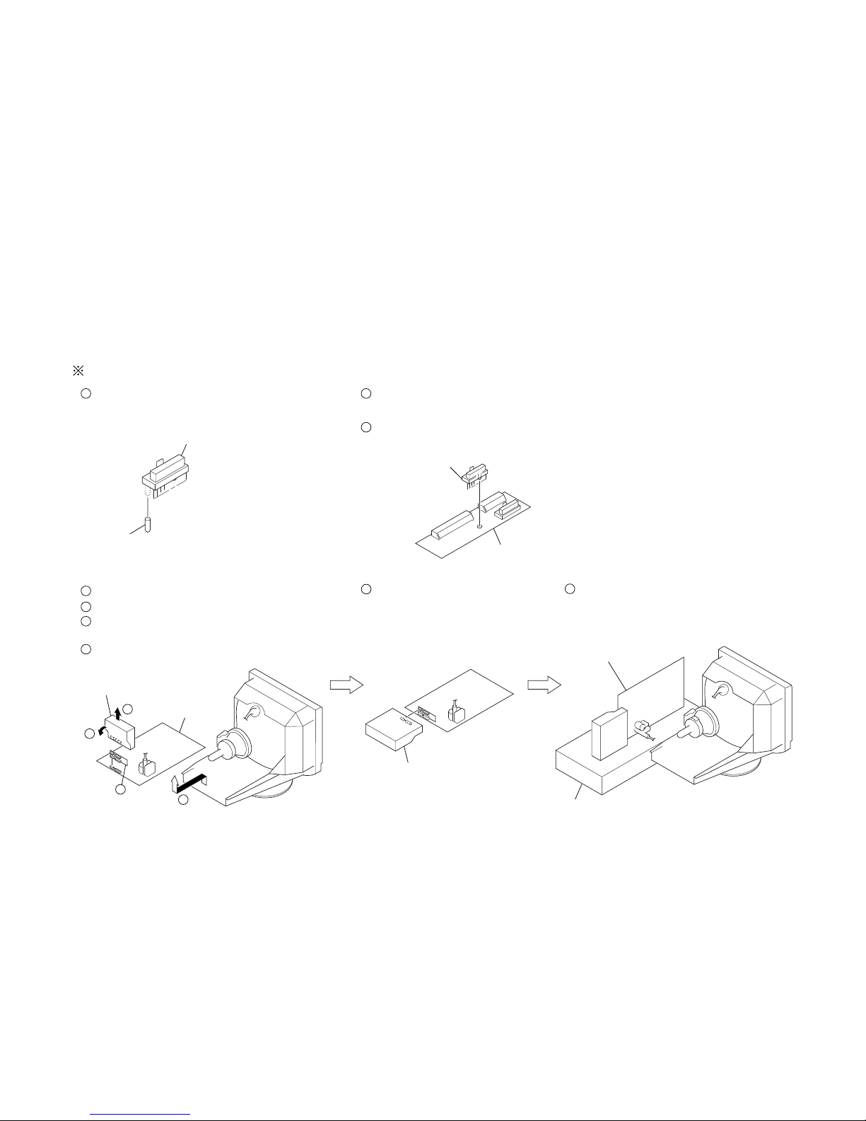
CPD-E430 (E) 1-6
4
5
7
4
Remove the D board.
D board
5
Remove the Video block assembly.
1
Prepare a connector (10Pin: Black) (1-766-921-11),
cut of the boss on the 10-pin side.
Adaptor board (XT Mount) is reconstructied to use for this set.
2
Remove the connector (17Pin: Black) (CN9997)
from Adaptor board (XT MOUNT) (A-1391-123-A).
3
Install the connector (10Pin: Black) onto XT Mount.
6
Install the Adaptor board
(XT MOUNT) (A-1391-123-A).
7
Lay the Video block assembly.
Video block assembly
Connector (10Pin: Black)
Boss
Connector
(10Pin: Black)
Adoptor board
(XT mount)
Video block assembly
8
Install the video block assembly.
9
Put a box which is about 15cm in height
under the D board to fix it.
(Please disconnect the CN 701 first.)
D board
Box
6
1-6. SERVICE POSITION
CPD-E430 (E) 1-7
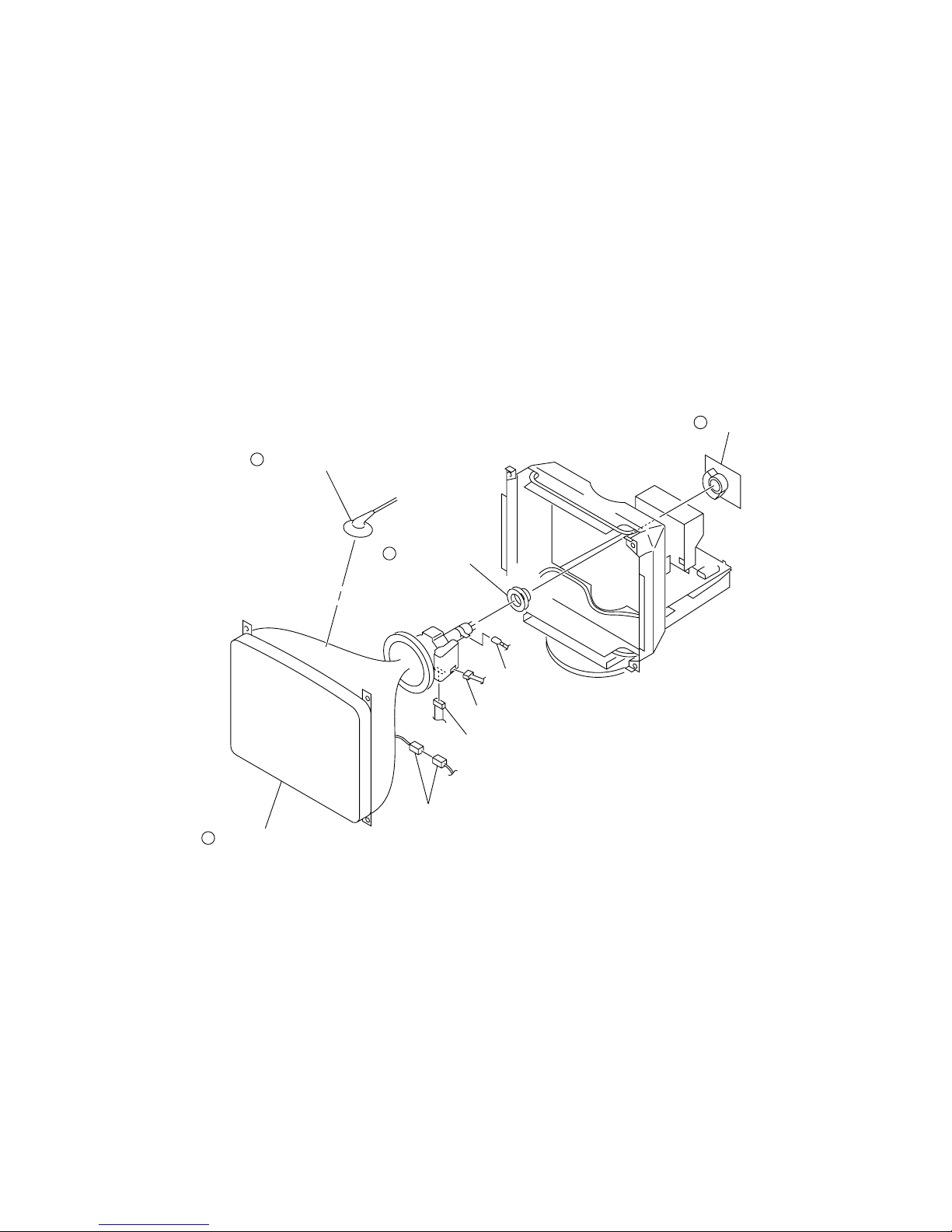
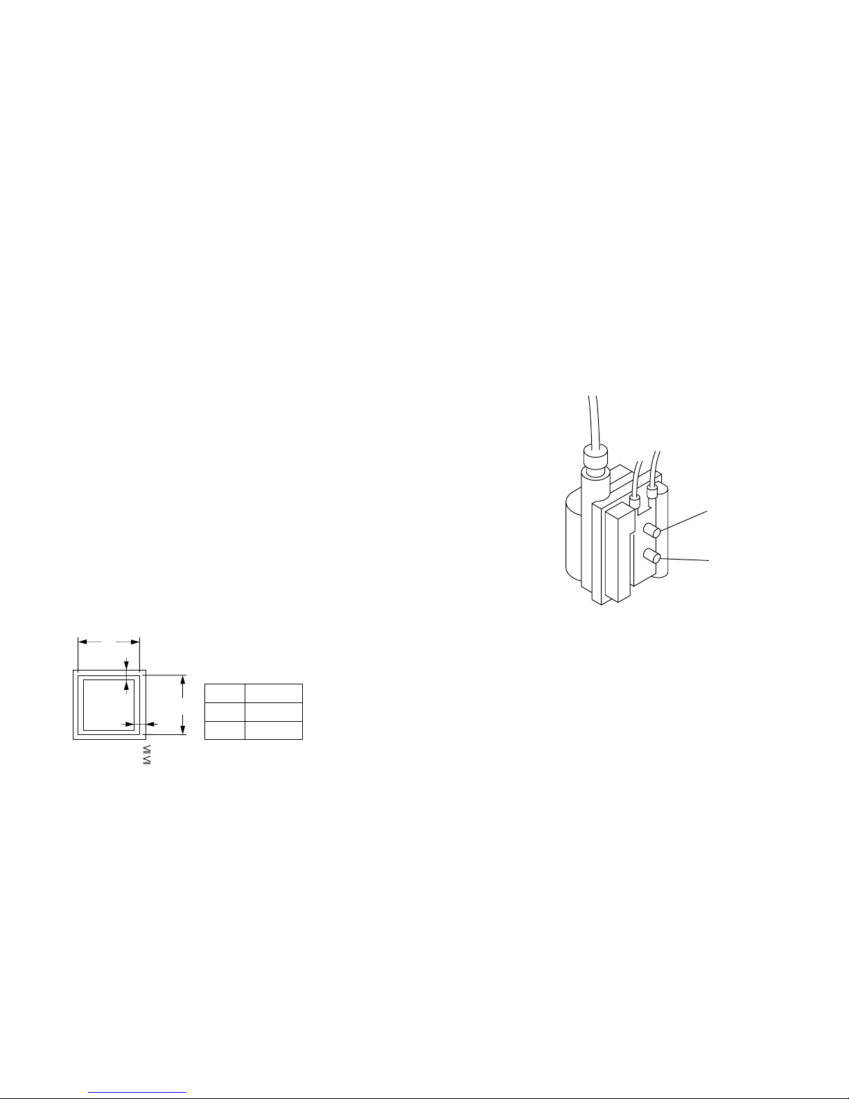
1-7. PICTURE TUBE REMOVAL
4
Picture tube
1
Anode cap (Refer to 1-8)
2
A board (C block)
3
Neck assembly
CN1
CN
Connector (2p)
GND
CPD-E430 (E) 1-8
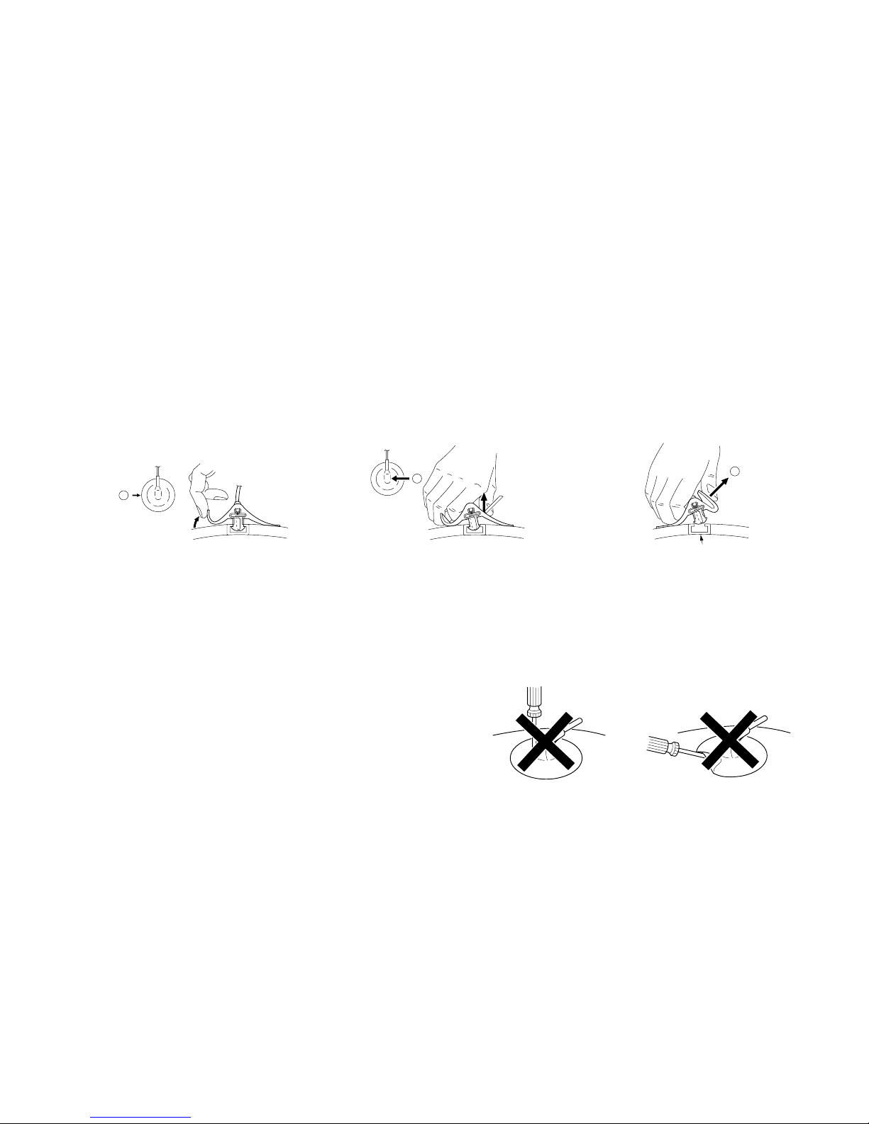
3When one side of the rubber cap is
separated from the anode button, the
anode-cap can be removed by turning up
the rubber cap and pulling up it in the
direction of the arrow c.
•HOW TO HANDLE AN ANODE-CAP
1Don’t scratch the surface of anode-caps with sharp shaped
material!
2Don’t press the rubber hardly not to damage inside of anode-
caps!
A material fitting called as shatter-hook terminal is built in the
rubber.
3Don’t turn the foot of rubber over hardly!
The shatter-hook terminal will stick out or damage the rubber.
•REMOVAL OF ANODE-CAP
NOTE: Short circuit the anode of the picture tube and the anode cap to the metal chassis, CRT shield or carbon painted on the CRT, after
removing the anode.
•REMOVING PROCEDURES
1Turn up one side of the rubber cap in the
direction indicated by the arrow a.
2Using a thumb pull up the rubber cap
firmly in the direction indicated by the
arrow b.
a
b
c
Anode Button
CPD-E430 (E) 1-9
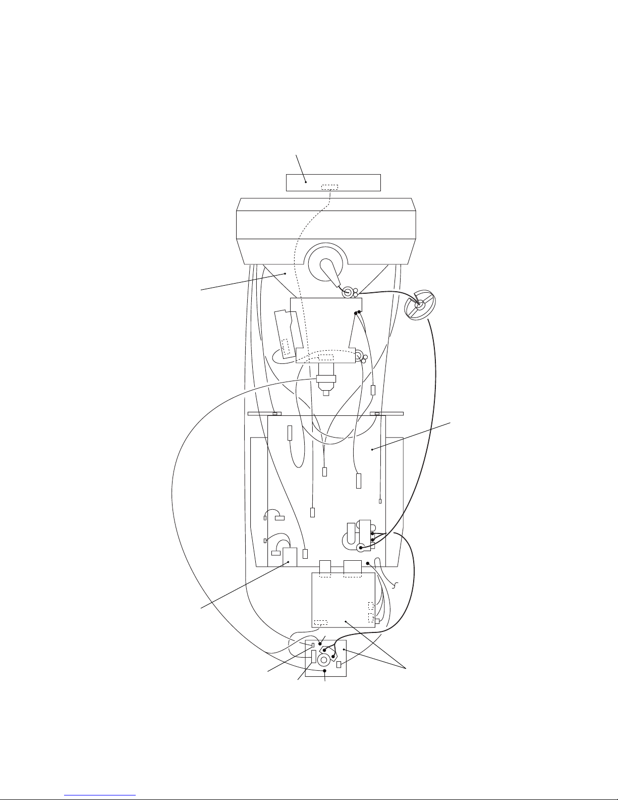
1-8. HARNESS LOCATION
CN600
CN602
CN601
CN604 CN1102
CN312 CN311
CN313
CN304
CN318
CN319
CN320
CN316
CN315
CN303
CN1
CN
CN1103
CN1400
CN1602
CN701
CN501
CN904
Picture tube
A board
D board
H1 board
AC inlet
CPD-E430 (E) 2-1
SECTION 2
SAFETY RELATED ADJUSTMENT
HV Regulator
Circuit Check
HV Protector
Circuit Check
When replacing or repairing the shown below table, the
following operational checks must be performed as a
safety precaution against X-rays emissions from the unit.
Part Replaced ([)
RV901
HV ADJ
* Confirm one minute after turning on the power.
a) HV Regulator Circuit Check
1) Turn the RV901 slowly, and adjustment so that high
voltage is in the specified range.
[Specification]: 27.00 ± 0.20 kV
2) Check that the voltage of D912 cathode on the D
board is 17.0 V or more.
b) HV Protector Circuit Check
1) Using external DC Power Supply, apply the voltage
shown below between cathode of D912 and GND,
and check that the RASTER disappers.
[Specification]: 19.85 + 0.00/– 0.05 V
Part Replaced (])
D Board C909, IC501, R901,
R902, R906, R910,
R913, RV901,
T901 (FBT)
• Mounted D Board
D Board C920, C923, D911,
D912, R903, R917,
R918, R919, R920,
R923, T901 (FBT)
• Mounted D Board
N Board IC1001, RB1001
• Mounted N Board
Beam Current
Protector Circuit
Check
Part Replaced (])
D Board C930, D917, R921,
R932, R933, R935,
T901 (FBT)
• Mounted D Board
N Board IC1001, RB1001
• Mounted N Board

CPD-E430 (E) 2-2
c) Beam Current Protector Circuit Check
1) Connect constant current source to a section between
T901 (FBT) qa pin and GND, and check that the
RASTER disappers when the specified current flows
to the qa pin.
[Specification]: 1.92 + 0.00/– 0.01 mA

CPD-E430 (E) 3-1
SECTION 3
ADJUSTMENTS
• Landing Rough Adjustment
1. Display all white pattern (or black dot pattern).
2. Set contrast to 255.
3. Display green plain pattern.
4. Side back DY and roughly adjust green plain pattern to be centered on
the useful screen with Purity Magnet.
5. Adjust DY tilt.
Note:Set ROTATION to 128 and LCC_NS to 128 when adjusting DY tilt.
6. Lightly tighten the DY screw.
• Landing Fine Adjustment
Note: (1) After adjust W/B (9300k), measure the average of ΣIK with all
white video input, while CONTRAST is maximum and
BRIGHTNESS is center. And adjustment shall be made so that the
miss-landing become least after aging 2H with the IK 30% of
measured value shown above.
(2) The magnetic field shall be BH = 0.
(3) When adjusting at other than BH = 0, calculate the shifted value
from BH = 0.
1. Put the monitor in helmholz coil.
2. Set as follows;
LCC_SW = 0 (LCC Correction Current = 0)
FUNCTION_SW bit1 = (Auto Degauss = On)
CONTRAST = 255
3. Display green plain pattern.
4. Degauss the iron part of chassis with a hand degausser and degauss coil.
5. Degauss CRT face with a hand degausser again.
6. Input AC 230V to AC IN and turn the monitor off and on. Then autodegauss works.
7. Reset FUNCTION_SW bit1 to 0 (auto-degauss = off)
8. Degauss CRT face with a hand degausser again.
9. Attach wobbling coil to the specified place on CRT neck.
10. With landing checker, adjust DY position, purity, DY center and
landing of the 4 corners.
11. Check landing of the 4 corners, and adjust using magnet if they are not
in the specification.
The red and blue must be within the
specification given right with respect to the
green.
A difference between red and blue must be
within the specification given right.
<Specifications>
Adjust so that the green is within the
specification given right.
4 corner adjust target : within ± 1
Note:(1) Do not attach more than 2 magnets on one corner.
(2) Attach magnets within the range of 80 - 100 mm from DY.
(3) Be sure to degauss and check when used magnets.
0 ± 3 0 ± 7.5 0 ± 3
0 ± 3 0 ± 7.5 0 ± 3
0 ± 3 0 ± 7.5 0 ± 3
(µm)
± 6 ± 6 ± 6
± 6 ± 6 ± 6
± 6 ± 6 ± 6
(µm)
10 10 10
10 7 10
10 10 10
(µm)
CPD-E430 (E) 3-2
a
b
cd
<How to place wedge>
Green plain crosshatch pattern
a and b should be equal.
c and d should be equal.
Plaster RTV to both sides for the upper wedge.
Make sure that they settle inside DY.
Plaster RTV to one side for other wedges.
12. Tighten DY screw within specified torque, and auto-degauss.
Note:Torque 22 ± 2 kgcm (2.2 ± 0.2Nm)
13. Adjust the vertical angle of DY to make top and bottom pins equal (a =
b). The horizontal angle shall not be changed (straight). Settle DY
upright without leaning, and insert wedges firmly so that DY shall not
move.
14. Adjust top and bottom pins correction VR.
15. Adjust the horizontal trapezoid distortion by DY horizontal trapezoid
correction VR.
16. Check landing at each corner and in case not in specification, adjust
landing of 4 corners with landing magnet.
17. Remove the sensor and wobbling coil.
18. Switch signals to R, G, and B, and then check that the pure colors have
good color purity.
19. Fix purity magnets with white paint.
CPD-E430 (E) 3-3
IBM AT Computer
as a Jig
1-690-391-211A-1500-819-A
Interface Unit
2
*The parts above ( ) are necessary for DAS adjustment.
1
3
D-sub
(9 Pin [female])
mini Din
(8Pin)
4 Pin
3-702-691-01
Connector Attachment
3
To BUS CONNECTOR
4 Pin 4 Pin
•Convergence Specification
B
A
A
0.20 mm
B
0.24 mm
V
XBVXCV
B
R
B
R
R
B
B
R
R
BBR
TLV
TLH
YBHYCH
R B
R B
H.TRAP
TB-PIN
TLH
XCV
Purity
4-pole magnet
6-pole magnet
2-pole magnet
Connect the communication cable of the computer to the connector located on the D board. Run the service software and then follow the instruction.
•Convergence Rough Adjustment
(1) Display white crosshatch pattern.
(2) Pile the convex parts of 6-pole magnet for convergence together.
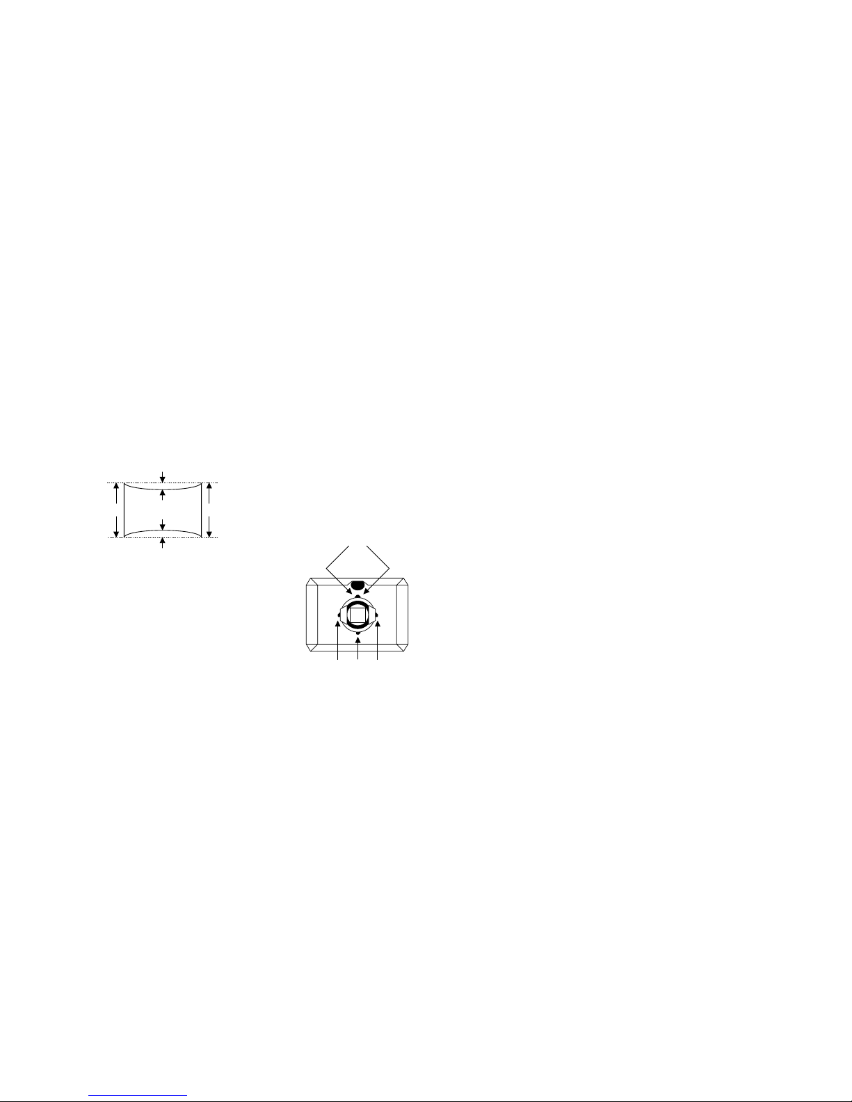
(3) Roughly adjust H.CONV and V.CONV with 4-pole magnet.
CPD-E430 (E) 3-4
B
a
a 1.8 mm
b 1.8 mm
a
b
b
A
MODE
A
B
4 : 3, 5 : 4
352
264
Focus 1
Focus 2
FBT
•White Balance Adjustment Specification
1. 9300 K
x = 0.283 ± 0.005
y = 0.298 ± 0.005
(All White)
2. 6500 K
x = 0.313 ± 0.005
y = 0.329 ± 0.005
(All White)
3. 5000 K
x = 0.346 ± 0.005
y = 0.359 ± 0.005
(All White)
•Vertical and Horizontal Position and Size
Specification
•Focus adjustment
Adjust the focus volume 1 and 2 for the optimum focus.
CPD-E430 (E) 4-1
SECTION 4
DIAGRAMS
4-1. BLOCK DIAGRAMS
A
TO D BOARD
CN1102
22
23
24
OSD R
OSD G
OSD B
OSD BLK
V_DET
BLK
CLAMP
26
28
30
8
9
11
2
4
7
R OUT
G OUT
B OUT
5
3
1
R OUT
G OUT
B OUT
B IN
G IN
R IN
R IN
G IN
B IN
COF R
COF G
COF B
SCL
SDA
20
19
SCL
SDA
9
SOG OUT
HD15
5
4
3
2
1
10
15
9
14
8
13
7
12
6
11
INPUT1
(HD15)
IC003
OSD
IC001
RGB PRE-AMP
IC002
RGB AMP
15 14 13 12
18 20 19 21
14
7
8
9
4
5
2
5
4
12
13
25
24
23
3
4
5
ROUT
GOUT
BOUT
XTAL IN
HS OUT
VS OUT
SCL
SDA
HS OUT
VS OUT
SCL
SDA
SCL
SDA
HS OUT
VS OUT
HS IN
VS IN
CS IN
RIN
GIN
BIN
IC004
CUT OFF AMP
IC011
HEATER REG
X001
24.5MHz
H FLY
OSD R
OSD G
OSD B
OSD BLK
AV
BLK
CLP
1
2
4
6
7
8
9
+B
+B
+80V
+12V
7V
3.3V
5V
+B
+80V
+12V
7V
3.3V
5V
CN312
G2
1
G2
CN318
5
3
1
7
KR
KG
KB
HEATER+
CN315
5
3
1
7
KR
KG
KB
HEATER+
FVFCHV
CN316
V901
PICTURE TUBE
7
101718
11
10
2
C
TO D BOARD
CN604
TO D BOARD
FBT
A
(VIDEO AMP, RGB OUT)
Vcc OUT
VADJ
7V
5
6
7
1
9
10
2
3
DDC GND
DDC SCL
DDC SDA
H BLK
IIC SCL
IIC SDA
HS OUT
VS OUT
CN311
CN304
9856
IC006
INVERTER
IC009
ROM
3 4 11 10
1 2 13 12
SDA
SCL
5
6
B
2
3
4
DDC SCL
DDC SDA
HOST GND
8
9
2
4
6
VD
HD
BLUE
GREEN
RED
CN313
24
IC005
INVERTER
SW
Q004
SW
Q005
B-SS3601<AEP>-BD1-EPS05
LED DRIVE
Q1400
D1400
A
G
LED DRIVE
Q1401
POWER
H1
(USER CONTROL)
1
2
3
4
T-AMB
KEY SCAN
LED1
LED2
CN1400
D
TO D BOARD
CN1103
5V
TH1400
S1406
BRIGHTNESS /
CONTRAST
S1405
MENU
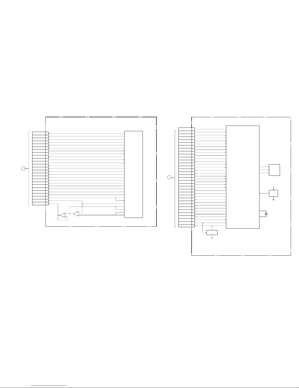
CPD-E430 (E) 4-2
B-SS3601<AEP>-BD2-EPS05
G
TO D BOARD
CN502
1
33
37
34
36
15
11
13
7
20
19
22
24
16
21
23
2
38
39
40
32
35
5
12
10
H.DF
REFDC
XDC
HD OUT
HFBP
H BLK
VS OUT
HS OUT
PLL LOCK
IIC SDA
IIC SCL
LCC_NS
HSAW_SW
H.LINBAL
GYSC
GXSC
V.DF
D.TILT
YSC
XSC
HSHAPE
YDC
POC
DCC2
VSAWN
CN1101
7
5
6
+
—
1
3
2
+
—
IC1102
AMP
DA
(DPU)
N
(
-COM
)
IC1001
CPU
1
2
3
21
23
35
36
38
39
40
41
43
44
45
48
49
50
51
52
53
54
63
27
26
64
58
59
61
62
IC1101
DPU
HDF1
DCC2
XDC
HDOUT
FBP-IN
H BLK
V-IN
H-IN
LOCK-DET
SDA
SCL
LCC_NS
HSAW_SW
PWM2
GYSC
GXSC
VDF
VKEY
YSC
XSC
HSHAPE
YDC
POC-OUT
POC-IN
DCC
ASW1
ASW2
VSAW L
VSAW H
P12/A10/AD10
P11/A9/AD9
P10/A8/AD8
RESET
X2
X1
64
63
62
46
7
6
5
IC1003
ROM
WC
SCL
SDA
5V
IC1002
RESET
I
G
O
41
43
X1001
16.9344MHz
INVERTER
Q1001
CN1001
I
TO D BOARD
CN1104
42
32
7
9
11
13
15
17
29
1
3
2
4
35
33
31
39
40
6
8
10
12
14
16
18
24
26
28
23
25
21
30
36
5
T-AMB
LB DET
DDC SDA1
DDC SCL1
DDC GND1
DDC SDA2
DDC SCL2
DDC GND2
INPUT SW
IIC SDA
IIC SCL
TXD
RXD
KEY SCAN
LED1
LED2
PLL LOCK
POC
HV DET
ABL DET
G2
S6
S5
S4
S3
S2
S1
S0
PWR SW
DGC SW
HTR SW
V.FBP
WAKE UP
ECO SW
P54/AN04
P42/AN10
P86/SDA1
P87/SCL1
P21/A1/A17
P84/SDA2
P85/SCL2
P20/A0/A16
P27/A7/A23
P80/SDA0/SI0
P81/SCL0/SO0
P82/TXD0
P83/RXD0
P42/AN11
P26/A6/A22
P25/A5/A21
P76/SCK0/INT3
P73/TB01N0/IN5
P57/AN07
P40/AN08
P70/TA1OUT
P36/TA7OUT
P35/TA61N
P34
P33/MAIT
P32/HWR
P31/WR
P30/RD
P04/AD4
P06/AD6
P05/AD5
P61/CTS0
P51/AN01
P60/INT0
16
21
51
52
71
49
50
70
80
35
36
37
38
23
79
78
34
31
19
20
28
7
6
5
4
3
2
1
58
59
60
10
13
9
 Loading...