

Page 1
SERVICE MANUAL
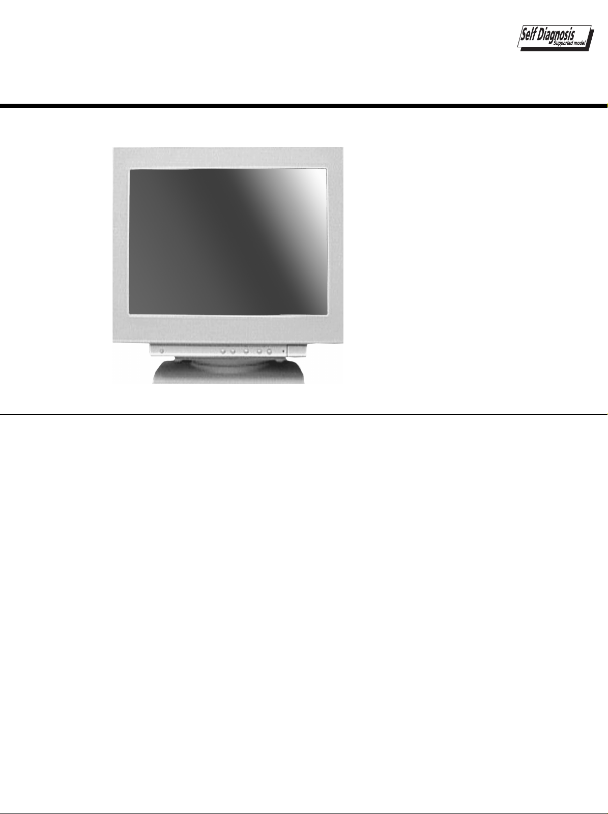
CPD-4401
CPD-4401
US Model
Canadian Model
AEP Model
Chassis No. SCC-L30N-A
Picture tube
Video image area
Resolution
Standard image
area
Input signal
Video
Sync
SPECIFICA TIONS
0.24 mm (center) -0.25mm (edge)
aperture grill pitch
19 inches measured diagonally
90-degree deflection
(18" maximum viewing image)
Approx. 364.8 X 273.6 mm (w/h)
3/8
7/8
x 10
x 10
7/8
inches)
1/2
inches)
(14
Horizontal: Max. 1600 dots
Vertical: Max. 1200 lines
Approx. 352 x 264 mm (w/h)
(13
Analog RGB (75 ohms typical)
0.7 Vp-p, Positive
Separate Horizontal and Vertical
TTL level, Positive or Negative
Video Composite (Sync on Green)
0.3 Vp-p
F99
Power Consumption
Maximum
Nominal
Deflection frequency
AC input voltage/current
Dimensions
Mass
CHASSIS
140 W, 478 BTU/h
100 W, 341BTU/h
Horizontal: 30 to 107 KHz (automatic)
Vertical: 48 to120 Hz (automatic)
100 to 120 V, 50/60 Hz,
1.8A (RMS) at 100VAC
220 to 240V, 50/60Hz,
1.0A (RMS) at 240 VAC
449 x 463 x 463 mm (w/h/d)
2/3
1/5
(17
x 18
Approx. 26.0 kg (57 lb 5 oz)
x 18
1/5
inches)
Design and specifications are subject to change without notice.
TRINITRON® COLOR MONITOR
Page 2
CPD-4401
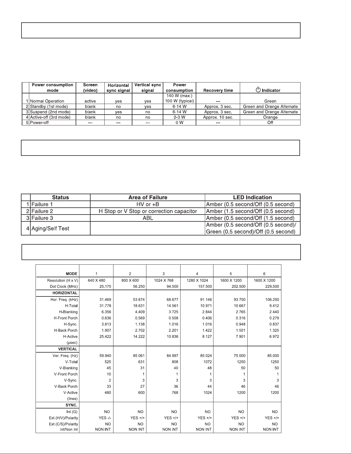
POWER MANAGEMENT MODES
If you have VESA's DPMS compliance display card or software installed in your PC, the monitor can automatically reduce
its power consumption when not in use. If input from keyboard, mouse, or other input devices is detected, the monitor
will automatically "wake up." The following table shows the power consumption and signaling of this automatic power
saving feature.
SELF DIAGNOSTIC FUNCTION
When a failure occurs, the STANDBY/TIMER lamp will flash a set number of times to indicate the possible cause of the
problem. If there is more than one error, the lamp will identify the first of the problem areas.
TIMING SPECIFICA TIONS
— 2 —
Page 3
1.5 k
Ω
0.15 µF
AC
Voltmeter
(0.75 V)
To Exposed Metal
Parts on Set
Earth Ground
SAFETY CHECK-OUT
CPD-4401
After correcting the original service problem, perform
the following safety checks before releasing the set to
the customer:
1. Check the area of your repair for unsoldered or poorlysoldered connections. Check the entire board surface
for solder splashes and bridges.
2. Check the interboard wiring to ensure that no wires
are “pinched” or contact high-wattage resistors.
3. Check that all control knobs, shields, covers, ground
straps, and mounting hardware have been replaced.
Be absolutely certain that you have replaced all the
insulators.
4. Look for unauthorized replacement parts, particularly
transistors, that were installed during a previous
repair. Point them out to the customer and
recommend their replacement.
5. Look for parts which, though functioning, show
obvious signs of deterioration. Point them out to the
customer and recommend their replacement.
6. Check the line cords for cracks and abrasion.
Recommend the replacement of any such line cord
to the customer.
7. Check the B+ and HV to see if they are specified
values. Make sure your instruments are accurate; be
suspicious of your HV meter if sets always have low
HV.
8. Check the antenna terminals, metal trim, “metallized"
knobs, screws, and all other exposed metal parts for
AC Leakage. Check leakage as follows.
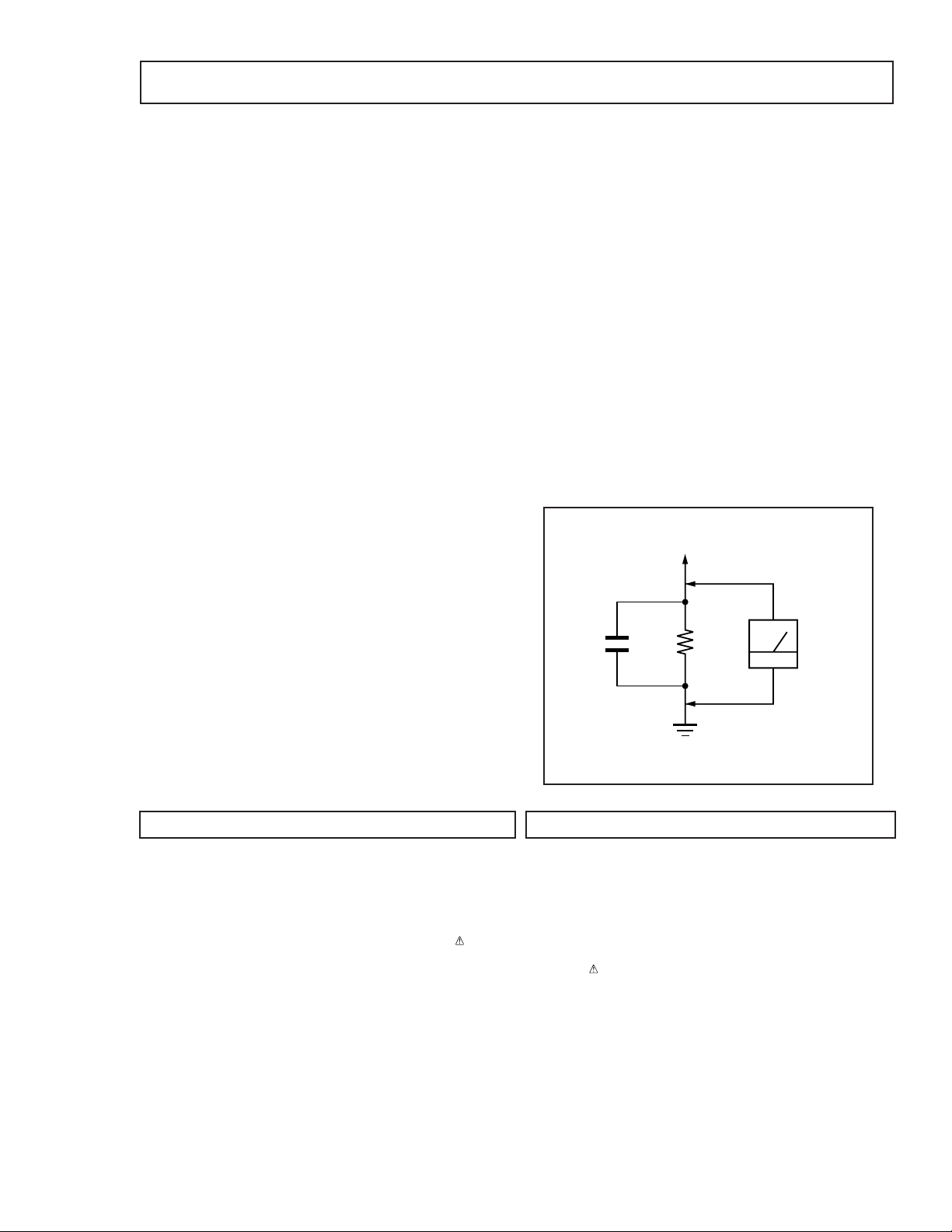
LEAKAGE TEST
The AC leakage from any exposed metal part to earth ground
and from all exposed metal parts to any exposed metal part
having a return to chassis, must not exceed 0.5 mA (500
microampere). Leakage current can be measured by any o ne
of three methods.
1. A commercial leakage tester, such as the Simpson 229
or RCA WT-540A. Follow the manufacturers' instructions
to use these instructions.
2. A battery-operated AC milliammeter. The Data Precision
245 digital multimeter is suitable for this job.
3. Measuring the voltage drop across a resistor by means
of a VOM or battery-operated AC voltmeter. The "limit"
indication is 0.75 V, so analog meters must have an
accurate low voltage scale. The Simpson's 250 and
Sanwa SH-63TRD are examples of passive VOMs that
are suitable. Nearly all battery operated digital
multimeters tha t hav e a 2V AC range are suitable. (See
Figure A)
WARNING!!
NEVER TURN ON THE POWER IN A CONDITION IN WHICH THE
DEGAUSS COIL HAS BEEN REMOVED.
SAFETY-RELA TED COMPONENT W ARNING!!
COMPONENTS IDENTIFIED BY SHADING AND MARK ON THE
SCHEMATIC DIAGRAMS, EXPLODED VIEWS AND IN THE PARTS
LIST ARE CRITICAL FOR SAFE OPERATION. REPLACE THESE
COMPONENTS WITH SONY P ARTS WHOSE PART NUMBERS APPEAR
AS SHOWN IN THIS MANUAL OR IN SUPPLEMENTS PUBLISHED BY
SONY . CIRCUIT ADJUSTMENTS THAT ARE CRITICAL FOR SAFE
OPERATION ARE IDENTIFIED IN THIS MANUAL. FOLLOW THESE
PROCEDURES WHENEVER CRITICAL COMPONENTS ARE REPLACED
OR IMPROPER OPERA TION IS SUSPECTED.
Figure A
AVERTISSEMENT!!
NE JAMAIS METTRE SOUS TENSION QUAND LA BOBINE DE
DEMAGNETISA TION EST ENLEVEE.
ATTENTION AUX COMPOSANTS RELA TIFS A LA SECURITE!!
LES COMPOSANTS IDENTIFIES P AR UNE TRAME ET P AR UNE
MARQUE SUR LES SCHEMAS DE PRINCIPE, LES VUES
EXPLOSEES ET LES LISTES DE PIECES SONT D'UNE IMPORT ANCE
CRITIQUE POUR LA SECURITE DU FONCTIONNEMENT. NE LES
REMPLACER QUE PAR DES COMPOSANTS SONY DONT LE
NUMERO DE PIECE EST INDIQUE DANS LE PRESENT MANUEL OU
DANS DES SUPPLEMENTS PUBLIES PAR SONY. LES REGLAGES
DE CIRCUIT DONT L'IMPORTANCE EST CRITIQUE POUR LA
SECURITE DU FONCTIONNEMENT SONT IDENTIFIES DANS LE
PRESENT MANUEL. SUIVRE CES PROCEDURES LORS DE CHAQUE
REMPLACEMENT DE COMPOSANTS CRITIQUES, OU LORSQU'UN
MAUV AIS FONTIONNEMENT SUSPECTE.
— 3 —
Page 4

CPD-4401
TABLE OF CONTENTS
Section Title Page
SAFETY CHECK-OUT ............................................................................. 3
1. GENERAL ........................................................................................ 5
2. DISASSEMBLY
2-1. Cabinet/Shield Removal ............................................. 1 0
2-2. Service Position ........................................................... 1 0
2-3. D, A, H and N Board Removal ..................................... 10
2-4. Picture Tube Removal ................................................. 11
3. SAFETY RELATED ADJUSTMENT ................................................ 12
4. ADJUSTMENTS ............................................................................ 13
5. DIAGRAMS
5-1. Block Diagram ............................................................. 1 5
5-2. Circuit Boards Location ............................................... 18
5-3. Schematic Diagrams and Printed Wiring Boards ...... 18
1. D Board - Schematic Diagram .............................. 1 9
2. H Board - Schematic Diagram .............................. 2 5
3. N Board - Schematic Diagram .............................. 2 6
4. A Board - Schematic Diagram ............................... 27
5-4. Semiconductors .......................................................... 3 0
6. EXPLODED VIEWS
6-1-1. Chassis (US/Canada Model) ................................... 3 2
6-1-2. Chassis (AEP Model) ................................................ 3 3
6-2. Packing Materials......................................................... 3 4
7. ELECTRICAL P ARTS LIST............................................................ 35
— 4 —
Page 5
The instructions given are partial abstracts from
4
Setup
Connect the monitor to your computer system.
This monitor will sync to platforms runningat horizontal
frequencies between 30 and107 kHz.
Step 1 Make sure the computer system is switched off and attach
the video signal cable to the video output of the computer.
Step 2 Make sure thecomputer is switched offand attach the
power cord to the monitor. Then, attach theother end o f
the power cord to a power outlet.
Step 3 Switch onthe monitor and computer.
Step 4 Adjust the user controlsaccordingto your personal
preference.
Installation is c omplete.
Identifying parts and
controls
1 (RESET) button (pages 6, 9)
This button resets theadjustmentsto the factory settings.
2 (AUTOSIZING AND CENTERING) button (page 5)
This button automatically fillsthe screen andadjusts vertical
and horizontal centering.
3 (BRIGHTNESS) (v/V) buttons (page 5)
These buttons adjust the picture brightnessand function as the
(v/V) buttons whenadjusting other items.
4 (MENU) button (page 6)
This button displays the MENU OSD.
5 6 (CONTRAST) (B/b) buttons(page 5)
These buttons adjust the contrast andfunction as the(B/b)
buttons when adjustingother items.
6 1 (POWER) switch and indicator
This button turns the monitor on and off.
The indicator lights up green when the monitoris on, andlights
up green and orange when the monitor is in Power Saving
mode.
7 AC IN connector
This connector provides AC power to the monitor.
8 Video input connector(HD15) (page 5)
This connector inputs RGB video signals and SYNC signals.
Computer
to the videooutput
to a poweroutlet
Power cord
Front
Rear
the Operating Instruction Manual. The page numbers shown reflect those of the Operating Instruction Manual
Precautions
Installation
Do not installthe monitor in the following places:
• on surfaces (rugs, blankets, etc.) or near materials (curtains,
draperies) that may block the ventilation holes
• near heat sources such as radiators or air ducts, or in a place
subject to direct sunlight
— 5 —
• in a place subject to severe temperature changes
• in aplace subject to mechanical vibration or shock
• on an unstablesurface
• near equipment which generates magnetism, such as a
transformer or high voltagepower lines
• near oron an electrically charged metalsurface
Maintenance
• Clean the screen witha soft cloth. If you use a glass cleaning
liquid, do not use any type of cleaner containing an anti-static
solution or similar additive as this may scratch the screen’s
coating.
• Do not rub, touch, or tap the surface of the screen with sharp or
abrasive items such as a ball point pen orscrewdriver. Thistype
of contact may result in a scratched picture tube.
• Clean the cabinet,panel and controlswith a softcloth lightly
moistened with a mild detergent solution. Donot use anytype of
abrasive pad, scouring powder orsolvent, such as alcoholor
benzene.
Transportation
When you transportthis monitor for repair or shipment, use the
original carton and packingmaterials.
Warning on Power Connection
• Use the supplied powercord. If you use a different power cord,
be sure thatit is compatiblewith your localpower supply.
For the customers in theUS
If you do not use the appropriate cord, this monitor will not
conform to mandatory FCC Standards.
Example of plug types
for 100 to120 V AC for 200 to240 V AC
• Before disconnecting the power cord, wait at least 30 seconds
after turning off the power to allow the static electricityon the
screen’s surface to discharge.
• After the power is turned on, the screen isdemagnetized
(degaussed) for about 3 seconds. This generates a strong
magnetic field aroundthescreen, which may affectdata stored on
magnetic tapes and disksplaced near the monitor. Besure tokeep
magnetic recording equipment, tapes and disks away from the
monitor.
The equipment should be installed near an easily accessible
outlet.
SECTION 1
GENERAL
US
3
CPD-4401
Page 6
CPD-4401
— 6 —
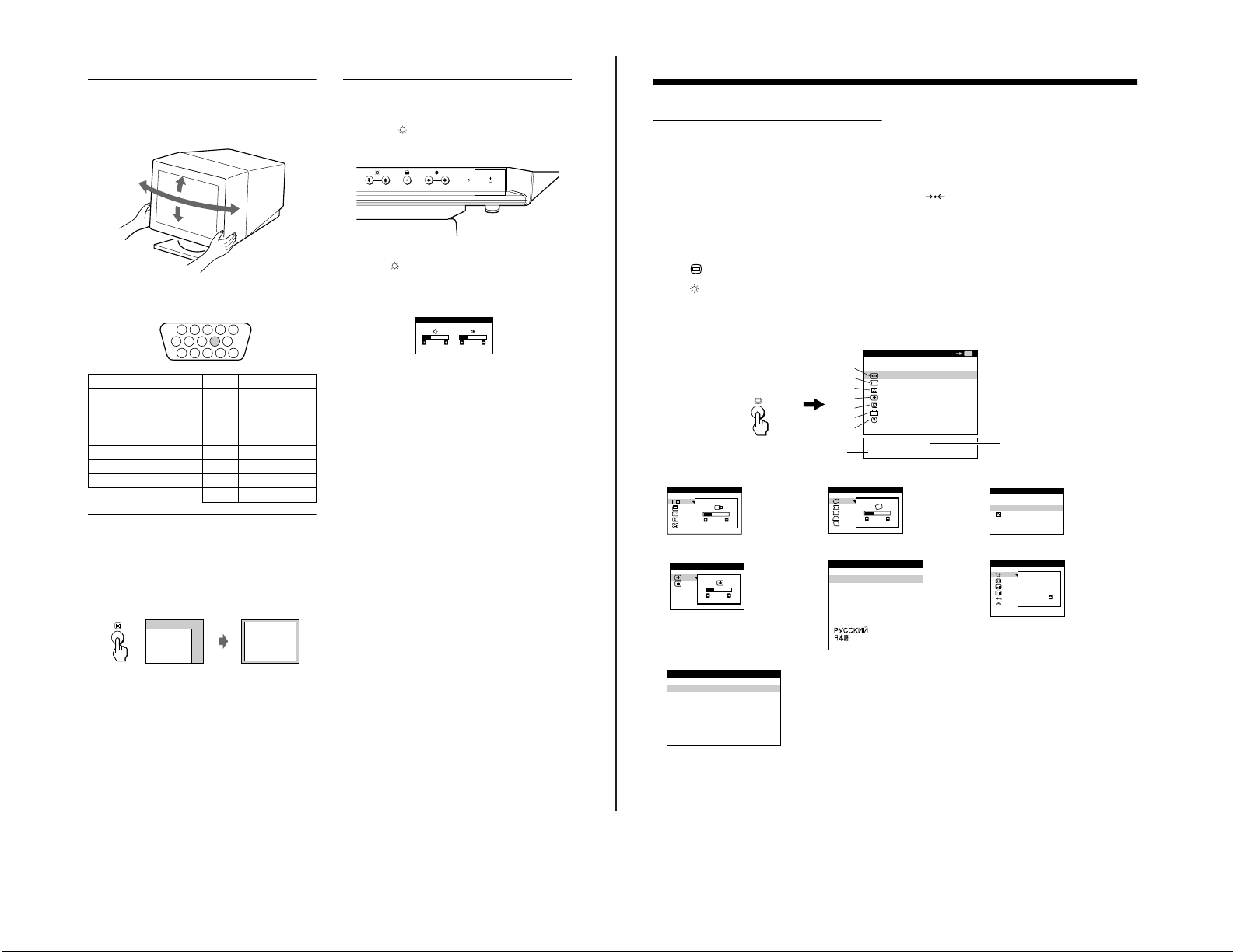
Use of the Tilt/Swivel
This monitor can be adjusted within the anglesshown below. To
turnthe monitor vertically or horizontally, hold it at the bottom with
both hands.
90°
15°
90°
5°
Video Connector
1234
6
11 12 13 14 15
Pin No. Signal Pin No. Signal
1 Red video 8 Blue return
2 Green video 9 Not used (no pin)
3 Blue video 10 Ground
4 Ground 11 Ground
5 CPU host ground 12 SDA(serial data)
6 Red ground 13 Horizontal Sync
7 Green return 14 Vertical Sync
5
987
10
15 SCL (serial clock)
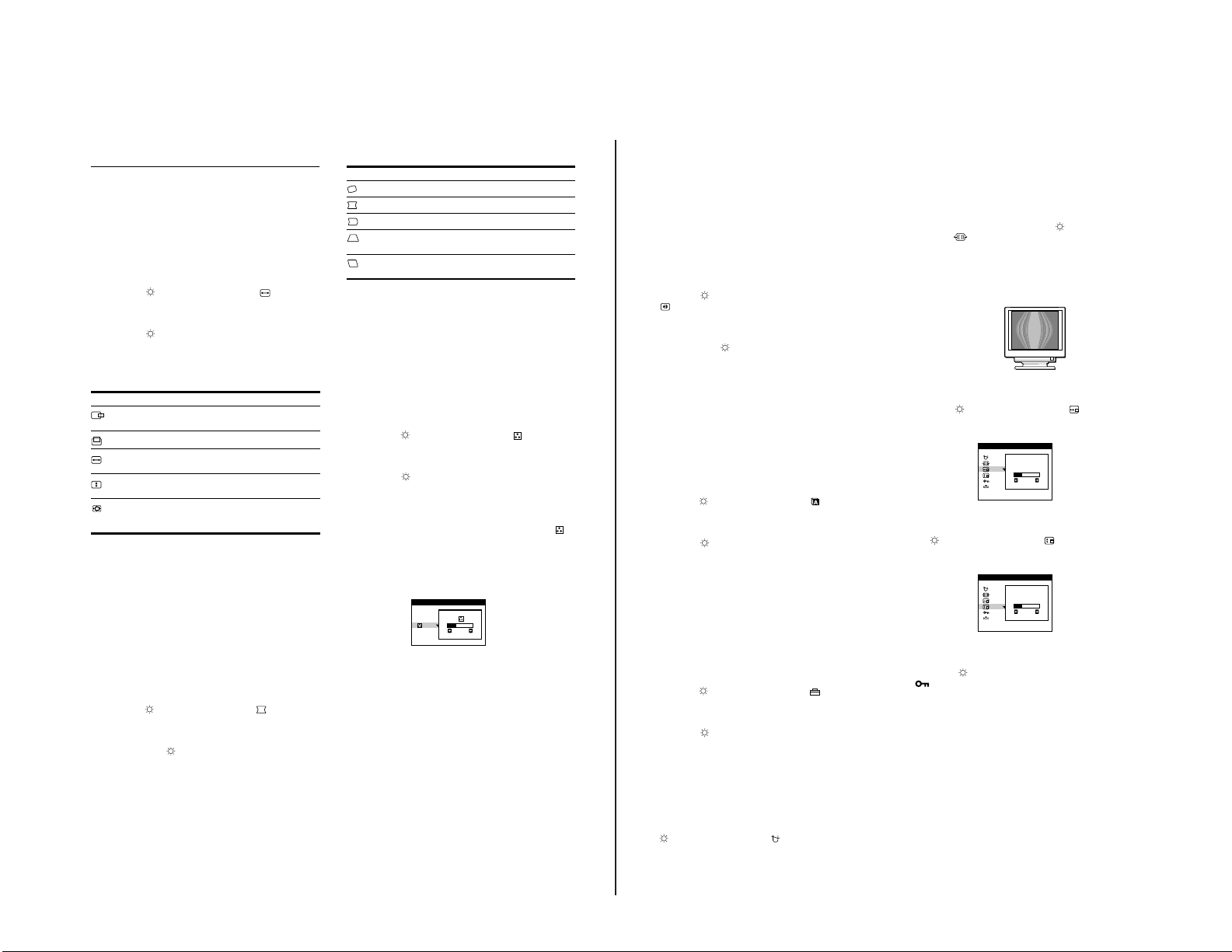
Automatically sizing and centering
the picture
You can easily adjust the picture to fillthe screen by pressing the
Auto Sizing and Centering button.
Press the Auto Sizing and Centering button.
The picture automaticallyfills the screen.
Adjusting the Picture Brightness
and Contrast
1 Press the (BRIGHTNESS)v/V or6 (CONTRAST)
B/b buttons.
The BRIGHTNESS/CONTRAST OSD appears.
2 To adjust the brightness.
Press the (BRIGHTNESS) v/V buttons.
To adjust the contrast.
Press the 6 (CONTRAST)B/b buttons.
BRIGHTNESS/CONTRAST
26 26
Customizing Your Monitor
The OSD (On-screen Display)
System
Introducing the OSD System
You can adjustmost of the monitor’s settings usingthe OSDs (OnscreenDisplay). All of the OSDs in this illustrationare described on
the following pages in order. You can access any of these OSDs
from the MENU OSD. To adjust monitorsettings using the OSDs,
follow the steps below:
Basic controls:
• Use the (MENU) button to display the MENU OSD and to
select menu items.
• Use the (BRIGHTNESS) v/V buttons to highlight menu
items and to adjust settings.
To adjust the monitor settings:
1 Press the MENU button to display the MENU OSD.
1
2
3
4
5
6
7
Resolutionfor current
input signal
1 SIZE/CENTER 2 GEOMETRY 3 COLOR
SIZE/CENTER
26
4 CONVERGENCE 5 LANGUAGE 6 OPTION
CONVERGENCE
26
GEOMETRY
LANGUAGE
ENGLISH
FRANÇAIS
DEUTSCH
ESPAÑOL
ITALIANO
NEDERLANDS
SVENSKA
2 Highlight the desired OSD using theBRIGHTNESS buttons and
press the MENU button again.
3 If necessary, use the BRIGHTNESS buttons to selecta specific
item.
4 Adjust the monitor setting using the BRIGHTNESS and
CONTRAST buttons.
• To reset the current item to itsoriginal setting, pressthe
(RESET) button whilethe item’s adjustmentOSD is
displayed.
5 When you finish adjustingthe setting,pressthe MENU button to
return to the MENU OSD.
Press the MENU button twice to return tonormal viewing.
• Resetting: Ifyou press theRESET button while an OSD is
displayed, only the current adjustment item is reset. For
additional information on using the resetfunction, see the
“Resetting the Adjustments” sectionon page 9.
• Each of the adjustment’s OSD automatically disappears after
30 seconds.
MENU
MENU
EXIT
SIZE/CENTER
GEOMETRY
COLOR
CONVERGENCE
LANGUAGE
OPTION
HELP
80.0kHz/ 75Hz
1280 X 1024
26
OK
Horizontal/Vertical
frequencies for
current input signal
COLOR
9300K
5000K
sRGB
OPTION
DEGAUSS
ON
Note
• This function isintended for use with a computer running Windows or
similar graphic user interfacesoftware that provides afull-screen picture.
It may not work properly if the background color isdark or if the input
picture does notfill the screen to theedges (such as anMS DOS prompt).
7 HELP
HELP
RETURN TO MAIN MENU
RECOMMENDED RESOLUTION
FLICKER
THIN HORIZONTAL LINE
DISTORTED SHAPE
OUT OF FOCUS
DISCOLORATION
5
6
Page 7
Adjusting the Settings
8
4 Adjusting the quality of the
picture (CONVERGENCE)
The CONVERGENCE settings allow you to adjustthe quality of
the picture by eliminating red or blue shadows aroundletters,
characters and lines.
Both settings arestored in memory for all input signals.
1
Press the MENU button.
The main MENU appears on the screen.
2
Press the v/V buttons to highlight
CONVERGENCE andpress the MENU button
again.
The CONVERGENCE menu appears on the screen.
3
First press the v/V buttons to selectthe desired
adjustment item. Then press the 6 B/b buttons to
adjust the setting.
The OSD automatically disappears after about 30 seconds. To
close the OSD, press the MENU button again.
5 Changing the OSD language
(LANGUAGE)
This setting is stored in memory for the current input signal.
1
Press the MENU button.
The main MENU appears on the screen.
2
Press the v/V buttonsto highlight LANGUAGE
and press the MENUbutton again.
The LANGUAGE menu appears on the screen.
3
Press the v/V buttons to select thelanguage you
prefer.
The OSD automatically disappears after about 30 seconds. To
close the OSD, press the MENU button again.
6 Additional settings (OPTION)
You can manually degauss (demagnetize) the screen, cancel the
moire, adjust theOSD horizontal position,adjust the OSD vertical
position and lockthe controls using the OPTION OSD.
1
Press the MENU button.
The main MENU appears on the screen.
2
Pressthe v/V buttons tohighlight OPTIONand
press the MENU buttonagain.
The OPTION menu appears on the screen.
3
Press the v/V buttons to highlight the desired
adjustment item.
Adjust the selected item according tothe following instructions.
The OSD automatically disappears after about 30 seconds. To
close the OSD, press the MENU button again.
Degaussing the monitor
The monitor isautomatically degaussed (demagnetized) whenthe
power is turned on.
To manually degauss the monitor, first press the
v/V buttons tohighlight (MANUAL DEGAUSS).
Then press only the right 6 b button.
The monitor is degaussed for about five seconds. If a second
degauss cycle isneeded, allow a minimum interval of 20
minutes for the best result.
Adjusting the moire
To adjust the moire, firstpress the v/V buttons to
highlight (MOIRE ADJUST). Then press the
6 B/b buttons to adjustthemoire until theeffect is at
a minimum.
* Moire is a type ofnatural interference which produces soft,wavy lines on
your screen. Itmay appear due to interference between the pattern of the
picture on the screen and the phosphor pitch pattern of the monitor.
Adjusting the OSD Horizontal Position
To changethe horizontalposition of the OSD,first
press the v/V buttons tohighlight (OSD H
POSITION). Then press the 6 B/b buttons to adjust
the horizontalposition of the OSD.
Adjusting the OSD Vertical Position
To change the verticalpositionof the OSD,firstpress
the v/V buttonsto highlight (OSD V
POSITION). Then press the 6 B/b buttons to adjust
the verticalposition of the OSD.
Locking the controls
To protect adjustment data by locking the controls,
first press v/V buttons tohighlight
(CONTROLLOCK). Then press the 6 B/b buttons
to togglethe ControlLock on or off.
Only the 1 (power) switchand MENU buttonwill operate.
Example of moire
OSD H
POSITION
OPTION
26
OSD V
POSITION
OPTION
26
1 Adjusting the size and centering
of the picture (SIZE/CENTER)
— 7 —
This setting is stored in memory for the current input signal.
1
Press the MENU button.
The main MENU appears on the screen.
2
Press the v/V buttons to highlight SIZE/
CENTER and press theMENU button again.
The SIZE/CENTER menuappears on the screen.
3
Press the v/V buttons to select the desired
adjustment item. Then press the 6 B/b buttons to
adjust the setting.
The OSD automatically disappears after about 30 seconds. To
close the OSD, press the MENU button again.
Select To
HORIZONTALCENTERING
VERTICAL CENTERING
HORIZONTALSIZING
VERTICAL SIZING
ZOOM
Note
Adjustment stops when either the horizontal or vertical size reaches its
maximum or minimum value.
shift the picture to the left or
right
shift the pictureup or down
enlargeorreducethepicture
width
enlargeorreducethepicture
height
enlargeorreducethepicture
width and height
proportionally
2 Adjusting the shape of the
picture (GEOMETRY)
The GEOMETRY settingsallow you to adjust therotation and
shape of thepicture.
The rotation settingis stored in memory for all input signals.All
other settings are stored in memoryfor the currentinput signal.
1
Press the MENU button.
The main MENU appears on the screen.
2
Press the v/V buttons to highlight GEOMETRY
and press the MENUbutton again.
The GEOMETRY menuappears on the screen.
3
First press the v/V buttons to selectthe desired
adjustment item. Then press the 6 B/b buttons to
adjust the setting.
The OSD automatically disappears after about 30 seconds. To
close the OSD, press the MENU button again.
Select To
ROT ATION
PINCUSHION
PIN BALANCE
KEYSTONE
KEY BALANCE
3 Adjusting the color of the picture
(COLOR)
The COLOR settings allow you to adjust thepicture’s color
temperature by changing the color level ofthe white color field.
Colors appear reddishif the temperatureis low, and bluish if the
temperature is high.This adjustment is useful for matchingthe
monitor’s colors toa printed picture’s colors.
This setting is stored in memory for allinput signals.
1
Press the MENU button.
The main MENU appears on the screen.
2
Press the v/V buttonsto highlight COLOR and
press the MENU buttonagain.
The COLOR menu appears on the screen.
3
Press the v/V buttons to select a color
temperature.
The preset color temperatures are 9300Kand 5000K. Since the
defaultsettingis 9300K, the whites change from a bluishhue to
a reddish hue as the temperature islowered to 5000K.
You can also fine tunethecolor temperature by selecting in
step 2 above,and using the 6 B/b buttons to adjustthe color
temperaturemanually.
You can choosethe optimal Brightness/Contrastsetting by
turning the sRGBfeature on. To turnit on, selectsRGB in step
2 above, and press the 6 b button.
This OSD allows you to adjust the colortemperature between
9300K and 5000K.
Press the 6 B/b buttons to adjustthe color temperature.
The OSD automaticallydisappearsafter about 30 seconds. To
close the OSD, press the MENU button again.
Note
The sRGB optimal setting will be undone once the brightness and/or the
contrast adjustment is made manually.
rotate the picture
expand or contractthe picture sides
shift the picturesides to the left orright
adjust the picturewidth at thetop of the
screen
shift the picture to theleft or right at the
top of the screen
COLOR
9300K
5300K
26
sRGB
7
CPD-4401
Page 8
Restoring the Color Image
11
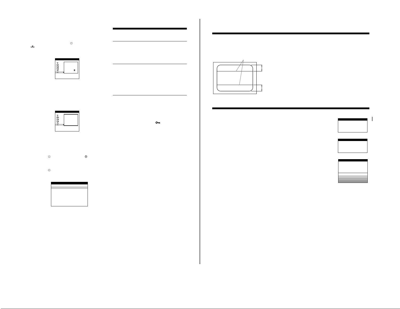
If Thin Lines Appear on Your Screen (damper wires)
The lines you may beseeing on your screen arenormal forthe Trinitronmonitor andare nota malfunction.These are shadowsfrom the damper
wires that stabilizethe aperture grille,and are most noticeable when the screen’s background islight (usually white).
The aperture grille is the essential elementthat makes aTrinitron picture tube uniqueby allowing more lightto reach thescreen, resulting in a
brighter, more detailedpicture.
Warning Messages
If there is something wrong with the input signal, one of the following messages appears.
To solve these problems, see the “Troubleshooting” section below.
1 OutofScanRange
This message indicates that the current input signal is not appropriate for the monitor’s specificatons.
2 Power Save Mode
This message indicates that themonitor has reduced powerconsumption.
3 Check Signal Cable (self test pattern)
This message indicates that either no input signal is received, or the video cable is not connected.
Damper wires
Approx. 7 cm
Approx. 7 cm
INFORMATION
MONITOR IS WORKING
OUT OF SCAN RANGE
CHANGE PC SETTING
INFORMATION
MONITOR IS IN
POWER SAVE MODE
ACTIVATE USING PC
INFORMATION
MONITOR IS WORKING
CHECK SIGNAL CABLE
RED
GREEN
BLUE
WHITE
The color of mostdisplay monitorstendto gradually lose brilliance
after several years of usage. The Image Restoration feature allows
you to restore the color to the original factory preset levels.
To restore the image, first press the v/V buttons to select
(COLOR RETURN). Then press the right 6 b button.
A white rectangle appears in the center of the screen while the
image is being restored (about two seconds).
OPTION
Resetting the adjustments
Resetting a specific adjustment
Navigate through theon-screen menus toselectthe adjustment item
you want to reset, and press the RESET button before the OSD
disappears.
CPD-4401
ON
COLOR
RETURN
— 8 —
Note
Before using this feature, the monitor must be in normaloperation mode for
at least 30 minutes.
If the monitor goes into power saving mode, you mustreturn the monitor to
normal operation mode and wait for 30 minutes forthe monitor to beready.
You may need toadjust your computer’s powersaving settings to helpkeep
the monitor in normaloperation mode for thefull 30 minutes. Ifthe monitor
is not ready, the following message will appear.
7 Using the HELP OSD
1
Press the MENU button.
The main MENU appears on the screen.
2
Press the v/V buttons to highlight HELP and
press the MENU buttonagain.
The HELP OSD appears on the screen.
3
Press the v/V to selectan optionfrom theHELP
menu, then press the MENU button to view theHELP
information.
OPTION
AVAILABLE
AFTER
WARM-UP
COLOR
RETURN
HELP
RETURN TO MAIN MENU
RECOMMENDED RESOLUTION
FLICKER
THIN HORIZONTAL LINE
DISTORTED SHAPE
OUT OF FOCUS
DISCOLORATION
Resetting all of the adjustments for
the current input signal
PresstheRESETbuttonwhennoOSDisdisplayedonthescreen.
Note that the following items are not resetby this method:
• on-screen menu language (page 8)
• on-screen menuposition (page 8)
Resetting all of the adjustment data
to the factory presets
Press and hold the reset button for morethan two seconds. This
resets everything to the factory presets.
Note
The RESET button does not function when
set to ON.
(CONTROL LOCK) is
9
Page 9

— 9 —
Troubleshooting
If the problemis caused by the connected computeror other equipment ,please refer tothe connected equipment’s instructionmanual.
Symptom Check these items
No picture
If the 1 (power) indicator is not lit • Check thatthe power cordis properly connected.
If the CHECK SIGNAL CABLE
message appears on the screen, or if
the 1 (power) indicator is either
orange oralternating between green
and orange
If the OUT OF SCAN RANGE
message appears on the screen
Picture flickers, bounces,
oscillates, or is scrambled
Picture is fuzzy • Adjust the brightnessand contrast (page 5).
Picture is ghosting • Eliminate theuse of video cable extensions and/orvideo switch boxes.
Picture is not centered or sized
properly
Edgesoftheimagearecurved • Adjust the geometry(page 7).
Wavy or ellipticalpattern (moire) is
visible
Color is not uniform • Degauss the monitor* (page 8). If you place equipment that generates a magnetic field, such
White does not look white • Adjust the color temperature (page 7).
Letters and lines show red or blue
shadows at the edges
Monitor buttons do not operate • IfthecontrollockissettoON,setittoOFF(page8).
A hum is heardright after the
power is turned on
* If a second degauss cycle is needed, allow a minimum interval of 20 minutes for the bestresult. A hummingnoise may beheard, but this is not a malfunction.
• Check thatthe 1 (power)switch is in the “on”position.
• Check that the video signal cable is properly connected and all plugs are firmly seated in
their sockets.
• Check that the HD15 video input cable’s pins are not bent or pushed in.
xProblems caused by the connectedcomputer orother equipment
• The computeris in powersaving mode. Try pressingany key on the computer keyboard.
• Check thatthe computer’s power is“on.”
• Check thatthe graphic video board is completely seated inthe proper busslot.
xProblems caused by the connectedcomputer orother equipment
• Check thatthe video frequency rangeis within that specified for the monitor. If you replaced
an old monitor withthismonitor,reconnect the old monitor andadjust the frequency rangeto
the following:
Horizontal: 30– 107kHz
Vertical:48 – 120 Hz
• Isolate and eliminate any potential sources of electric or magnetic fields such as other
monitors, laser printers,electric fans, fluorescentlighting and televisions.
• Move the monitor away from power lines or place a magnetic shield near the monitor.
• Try plugging the monitor into a different AC outlet,preferably on adifferent circuit.
• Try turning the monitor 90° to the left or right.
xProblems caused by the connectedcomputer orother equipment
• Check yourgraphicvideo board manualfor the proper monitorsetting.
• Confirm that the graphics mode (VESA,VGA, etc.) and the frequencyof the input signal are
supported by thismonitor (Appendix). Evenif the frequencyis within the proper range,
some graphic videoboards may have a sync pulse that is toonarrow for the monitor to sync
correctly.
• Adjust the computer’s refresh rate (vertical frequency)to obtain the best possible picture.
• Degauss themonitor* (page 8).
• Adjust the moire (page 8).
• Check that all plugs are firmly seated in their sockets.
• Adjust the size (page 7) or centering (page 7).Note that somevideo modes do not fill the
screen to the edges.
• Adjust the moire (page 8).
xProblems caused by the connectedcomputer orother equipment
• Change your desktop pattern.
as a speaker, near the monitor, or if you change the direction the monitor faces, color may
lose uniformity.
• Adjust the convergence (page 8).
• This is thenormalsound of the auto-degauss cycle. When thepoweris turned on, the monitor
is automatically degaussed for 5 seconds.
12
CPD-4401
Page 10
CPD-4401
SECTION 2
DISASSEMBLY
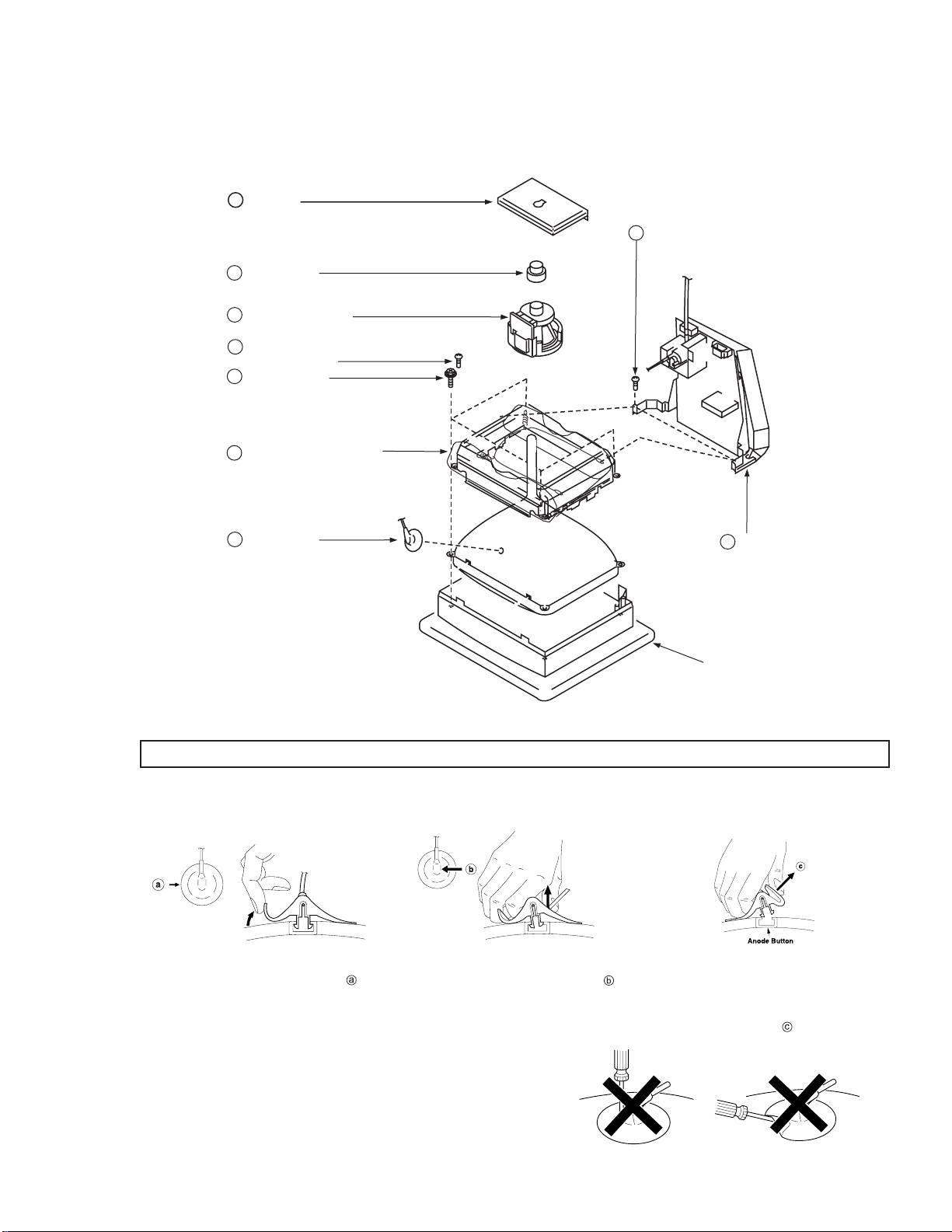
2-1. CABINET/SHIELD REMOVAL
Push in the tip of a screwdriver
about 5mm to unlock the claw.
4
Four screws
(+ BVTP 4 x 8)
5
8
Three screws
(+BVTT 4 x 8)
9
Side cover
Top cover
9
Side cover
T o remove the rear cover of the unit, press in and unsnap the claw on
the right side of the unit, then press in and unsnap the right claw at
the top of the unit. Repeat this with the claw on the left side and
top left of the unit and remove.
Bezel assembly
7
8
Three screws
(+BVTT 4 x 8)
6
Video shield
2-2. SERVICE POSITION
Cabinet
1
Two screws
(+ BVTP 4 x 16)
Cabinet
2
Two claws
1
A board
1 When the D board is placed in service position, the Safety Earth Wire
(black wire) is disconnected.
2 After service is completed and the D board reinstalled, the Safety Earth
Wire must be reattached to the chassis. This must be confirmed before
any subsequent procedures are attempted.
Cabinet
2
Two claws
Three screws
(+BVTT 4 x 8)
Bezel assembly
3
rotate 180º
2
D board
2-3. D, A, H and N BOARD REMOVAL
9
Two screws
(BVTT 4 x 8)
11
H board
10
N board
8
D board
7
One screw
(BVTT 4 x 8)
6
Five screws
(BVTP 3 x 8)
5
Holder
7
One screw
(BVTT 4 x 8)
3
One screw
(BVTT 4 x 8)
4
Cable bracket
2
A board
1
Three screws
(BVTT 4 x 8)
— 10 —
Page 11
2-4. PICTURE TUBE REMOVAL
2
A board
3
Neck ass'y
4
Deflection yoke
5
Two screws
(BVTP 4 x 16)
6
Four screws
(Tapping screw 5)
Picture tube shield
9
Demagnetization coil
Tension spring
7
Two screws
(BVTP 4 x 16)
CPD-4401
1
Anode-cap
8
Stand
ass'y
(D board)
Cushion
REMOVAL OF THE ANODE-CAP
WARNING: Short circuit the anode of the picture tube and the anode-cap to the metal chassis, CRT shield or carbon painted on the
CRT, after removing the anode.
REMOVAL PROCEDURES
1. Turn up one side of the rubber cap in
the direction indicated by arrow .
HOW TO HANDLE AN ANODE-CAP
1. Do not use sharp objects which may cause damage to the surface
of the anode-cap.
2. Do not squeeze the rubber covering too hard to avoid damaging the
anode-cap. A material fitting called a shatter-hook terminal is built into
the rubber.
3. Do not force turn the foot of the rubber cover. This may cause the
shatter-hook terminal to protrude and damage the rubber.
2. Use your thumb to pull the rubber cap firmly
in the direction indicated by arrow .
3. When one side of the rubber cap
separates from the anode button, the
anode-cap can be removed by turning
the rubber cap and pulling it in the
direction of arrow .
— 11 —
Page 12
CPD-4401
SECTION 3
SAFETY RELA TED ADJUSTMENT
When replacing parts shown in the table below, the following
operational checks must be performed as a safety precaution
against X-ray emissions from the unit.
Part Replaced ( )
HV ADJ RV901
Part Replaced ( )
HV Protector T901 (FBT), R917, R918, R923, R920,
Circuit R919, R1004, C920, D911, D912
Beam Current R933, R932, R921, R1006, D915,
Protector Circuit D917, IC901, T901 (FBT)
HV Regulator T901 (FBT), IC901, R924, R925,
Circuit RV901
Allow the unit to warm-up for one minute prior to checking
the following conditions:
HV Regulator Check
1) Input white cross hatch signal. (fH = 106.3 kHz)
2) CONT and BRT Control normal condition.
3) Input voltage: 120 ± 2 VAC
4) Confirm that the voltage is within the voltage range shown
below.
Standard voltage: 27.0KV ± 0.2KV
5) When replacing components identified by
sure to recheck the High Voltage.
6) Verify the High Voltage as shown above (27.0KV
+0.2KV) is within specification. If not, RV904 on D board.
7) After adjusting the High Voltage within specification, put
the RV cover on RV901 as shown below and apply
sufficient amount of RTV around RV901.
, make
HV Protector Check
1) Confirm the voltage more than 15.0 VDC between D912
cathode and GND on D Board.
2) Using an external DC power supply, apply the voltage
shown below between cathode of D915 on D Board and
GND.
Confirm that the HV protector circuit (Hold down) works
and CRT screen disappears when applying the voltage
protector as shown below.
Standard DC Voltage: 21.1 +0.00 / - 0.05 VDC
Check Condition
• Input voltage : 120 ± 2 VAC
• Input signal : (fH = 31.4 kHz), Cross Hatch
• CONT and BRT Control: Normal Condition
Beam Current Protector Check
(Software Logic)
1) Using an external current source, apply 1.68mA from pin
of T901 (FBT) to GND on D Board. Confirm that the
software logic beam current protector works and that the
CRT screen disappears.
Check Condition
• Input voltage : 120 ± 2 VAC
• Input signal : (fH = 31.4 kHz), Cross Hatch
• CONT and BRT Control: Normal Condition
B± Maximum Check
1) Input white cross hatch (fH = 106.3 kHz) signal.
2) Beam control: Normal condition
3) Input voltage: 100 - 120 VAC
Note: Use NF power supply or make sure that
distortion factor is 3% or less.
4) Confirm that the voltage is within the voltage range
shown below.
Standard voltage: 195.0 -205.0 VDC
RV901
— 12 —
Page 13
CPD-4401
a
b
SECTION 4
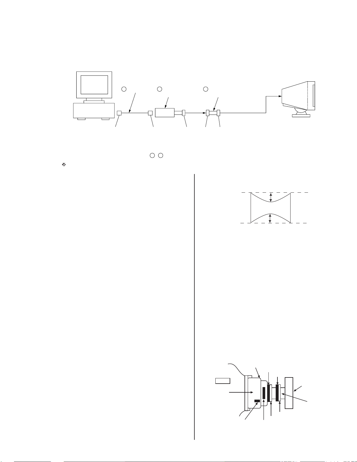
ADJUSTMENTS
Connect the communication cable of the connector located on the D board on the monitor. Run the service software and then foll ow
these instructions.
IBM AT Computer
as a Jig
1-690-391-21
1
D-sub
(9 Pin [female])
*The parts above ( ~ ) are necessary for DAS adjustment.
mini Din
(8Pin)
1
A-1500-819-A
2
Interface Unit
3
4 Pin
3
4 Pin 4 Pin
Allow a 30 minute warm-up period prior to making the following adjustments:
4-1. Landing Rough Adjustment
1. Enter the full white signal.
2. Adjust the contrast to the maximum.
3. Input full green signal.
(Note: Turn off the outputs from R ch and B ch of SG)
4. Move the DY backward and adjust the purity magnet
coarsely so that a green raster positions in the center of
screen.
5. Moving the DY forward, adjust so that an entire screen
becomes pure green.
6. Adjust DY Tilt, use TLV of DY for this adjustment. Fix
the
Register "TILT" to 0.
7. Lightly tighten the DY screw.
3-702-691-01
Connector Attachment
To BUS CONNECTOR
Fasten wedges so that DY does not move.
14. If landing does not meet specifications, correct with a
disc magnet.
15. Perform auto-degauss.
16. Remove sensor and wobbling coil.
17. Confirm that there is no DY tilt. Affix purity magnet on
DY using white paint.
4-2. Landing Fine Adjustment
1. Place the set in the Helmholtz coil.
2. Set TLH plate to the zero position.
3. Adjust Purity Magnet on the Neck Assembly to zero
position and secure it with white pin.
4-3. Convergence Rough Adjustment
1. Enter the white crosshatch signal.
2. Roughly adjust the H. STAT and V. STAT with a
four-pole magnet.
3. Roughly adjust HMC and VMC with a six-pole magnet.
4. Set "VPIN SAW TOP" and "VPIN SAW BTM" to zero
position.
5. Display a plain green pattern.
6. Degauss CRT and shield with hand-degausser .
7. Perform auto-degauss.
4-4. Convergence Fine Adjustment
1. Display crosshatch pattern with R and B.
2. Adjust H. STAT and V. STAT with 4-pole magnet.
(Do not adjust H.STAT and V.STAT with resistor.)
8. Attach a wobbling coil to the specified position of CRT.
9. Attach a landing adjuster sensor on the CRT.
10. Using a landing checker, adjust the DY position, purity,
tilt of DY.
11. Tighten the DY screw.
Clamping torque: 22 ± 2 kg.cm (2.2 ± 0.2 N.m)
12. Perform auto-degauss.
13. Adjust top and bottom pin pitching DY by up and down
with two wedges so that (a) is equal to (b)(see the figure
at right). Also, leave the yaw of DY to the physical
center position with another two wedges.
CRT
DY
TLV VR (Unused)
XCV Core
2 Pole
6 Pole Mg
A Board
Neck Assy
2 Pole (Unused)
4 Pole Mg
TLH Plate
— 13 —
Page 14

CPD-4401
3. Display white crosshatch pattern.
4. Adjust HMC and VMC with 6-pole magnet.
5. Display crosshatch pattern with R and B.
6. Adjust H.STAT and V.STAT with 4-pole magnet.
7. Fine adjust H. STAT and V. STAT with use register
'HSTAT" and "VSTAT" in the range of 0 ± 10.
8. Adjust H.TILT with TLH plate.
Move of THL Plate
or
9. Adjust XCV with XCV core.
Move of XCV Volume
or
10. Repeat steps 2-8 to optimize condition of whole screen.
11. Affix 4-pole magnet, 6-pole magnet and TLH plate and
XCV core with white paint.
4-7. Vertical and Horizontal Position and
Size Specification
B
b
b
a
a
fH < 60 KHz
2.4 mm
2.4 mm
A
fH > 60 KHz
a
< 2.0 mm
b
< 2.4 mm
A B
264 352
4-8. Convergence Specification
C
A
Horizontal and Vertical
B
Prime Mode
A
< 0.25 mm
B
< 0.30 mm
C
< 0.35 mm
Other Mode
0.30 mm
0.35 mm
0.40 mm
4-9. Focus Adjustment
Adjust focus (V) and focus (H) for optimum focus.
4-5. Zero Positions of Ring Magnets
are Indicated by Arrows
[2pole magnet on DY] [4pole magnet]
[2pole magnet on Neck Assy][6pole magnet]
4-6. White Balance Adjustment
Specification
1. 9300K
x=0.283
y=0.298
2. 5000K
x=0.346
y=0.359
+0.015
+0.015
(All White)
+0.015
+0.015
(All White)
— 14 —
Page 15

5-1. BLOCK DIAGRAM
CPD-4401
SECTION 5
DIAGRAMS
5-2. CIRCUIT BOARDS LOCATION
A
N
H
D
5-3. SCHEMATIC DIAGRAMS AND PRINTED WIRING BOARDS
Note:
• All capacitors are in µF unless otherwise noted. pF: µµF 50
WV or less are not indicated except for electrolytic.
• Indication of resistance, which does not have one for rating
electrical power, is as follows.
Pitch: 5 mm
Rating electrical power 1/4 W (CHIP: 1/10 W)
• All resistors are in ohms.
• : nonflammable resistor .
•
•
•
: fusible resistor.
: internal component.
: panel designation and adjustment for repair.
• All variable and adjustable resistors have characteristic curve
B, unless otherwise noted.
• : earth-ground
•
: earth-chassis.
• The components identified by in this basic schematic
diagram have been carefully factory-selected for each set in
order to satisfy regulations regarding X-ray radiation. Should
replacement be required, replace only with the value
originally used.
• When replacing components identified by
, make the
necessary adjustments by using RV901 ( ) as indicated.
(See page 12)
Note: The components identified by shading and
mark are critical for safety. Replace only with
part number specified.
• When replacing parts shown in the table below, be sure to
perform the safety related adjustment.
HV ADJ
HV Regulator
Circuit
HV Protector
Circuit
Beam Current
Protector
Circuit
• All voltages are in volts.
• Readings are taken with a 10 M W digital multimeter
• Readings are taken with a color-bar signal input.
• Voltage variations may be noted due to normal production
tolerances.
• * : Cannot be measured.
• Circled numbers are waveform references.
•
•
: B +bus.
: B - bus.
Part Replaced ( )
RV901
Part Replaced ( )
D board T901, IC901, R924, R925,
RV901
D board T901, R917, R918, R923, R920,
R919, R1004, C920, D911,
D912
D board R933, R932, R921, R1006,
D915, D917, IC901, T901
866 Block Diagram.p65 10/15/1999, 8:14 AM1
Note: Les composants identifies per un trame et une
marque sont critiques pour la securite. Ne les
remplacer que par une piece portant le numero specifie.
— 18 —— 17 —— 16 —— 15 —
Page 16

CPD-4401
D BOARD SCHEMATIC DIAGRAM
A
B
C
D
1234
56789101112131415
16 17 18 19
20
D BOARD WAVEFORMS
123
5.8 Vp-p (H) 4.8 Vp-p (V)
456
12.9 Vp-p (H) 12.8 Vp-p (H) 1.14 KVp-p (H)
789
3.3 Vp-p (8MHz)
E
F
G
H
12.3 Vp-p (H) 18.7 Vp-p (H) 10.4 Vp-p (H)
10 1 1 12
1.14 Vp-p (H) 70.0 Vp-p (H) 1.5 Vp-p (V)
13
55.0 Vp-p (V)
K
M
I
D BOARD LOCATOR LIST
DIODE
J
L
D401 I-5 D611 A-8 D705 H-1 D1010 C-2 IC702 J-4 Q517 C-3
D402 H-2 D612 A-7 D901 H-9 D1011 C-2 IC703 B-2 Q519 C-4
D405 I-5 D613 B-6 D903 H-10 D1012 C-2 IC901 G-10 Q605 B-7
D501 F-8 D614 D-9 D904 H-10 D1013 C-2 IC1001 D-1 Q606 D-8
D502 G-10 D615 D-8 D906 E-12 D1014 C-2 IC1003 C-3 Q607 D-10
D503 F-6 D616 E-8 D907 F-12 D1018 C-1 IC1005 D-2 Q608 D-13
D504 F-8 D617 E-8 D908 H-10 D1021 E-1 Q609 B-4
D505 F-6 D618 D-8 D909 E-11 D1022 E-1 Q501 F-3 Q701 I-8
D506 F-3 D619 E-7 D910 G-12 D1024 C-3 Q502 F-2 Q702 H-8
D507 G-1 D620 D-7 D911 H-13 D1025 E-2 Q503 F-2 Q703 I-8
D508 G-1 D621 D-7 D912 I-13 Q504 F-9 Q704 I-7
D509 F-2 D622 D-6 D913 I-13 IC401 I-6 Q505 H-8 Q705 I-7
D510 F-1 D623 D-4 D914 I-13 IC501 F-1 Q506 F-5 Q706 J-11
D511 G-1 D624 C-5 D915 J-12 IC502 C-5 Q507 F-3 Q901 E-13
D512 G-1 D625 C-11 D916 I-12 IC503 G-1 Q508 G-3 Q902 E-11
D514 C-4 D626 D-11 D917 I-9 IC603 A-7 Q509 G-2 Q903 G-10
D515 C-4 D627 D-10 D920 H-1 IC604 D-5 Q510 F-4 Q904 H-11
D516 F-6 D628 D-12 D921 H-1 IC605 D-4 Q511 G-5
D517 I-8 D629 A-3 D1001 E-2 IC607 A-6 Q512 H-5 X1001 D-2
D518 B-4 D630 A-5 D1003 D-2 IC608 A-6 Q513 H-4
D608 A-6 D701 H-8 D1007 C-3 IC609 B-4 Q514 H-3
D609 B-8 D702 H-8 D1008 C-3 IC610 B-5 Q515 G-4
D610 A-6 D703 I-8 D1009 E-2 IC701 I-2 Q516 F-3
TRANSISTOR
IC
CRYSTAL
N
board
D
866 D Schematic .p65 10/13/1999, 3:16 PM1
— 22 —— 21 —— 20 —— 19 —
Page 17

D
[CONVERGENCE, DEFLECTION, POWER]
H BOARD SCHEMATIC DIAGRAM
CPD-4401
N BOARD SCHEMATIC DIAGRAM
C
D
A
B
1234
5678910111213
A
B
C
D
1234
56
A
B
C
D
1234
5678
E
F
G
H
E
F
[DSP]
N
(COMPONENT SIDE)
123
[FUNCTION CONTROL]
1234A5678
I
A
B
A
B
[DSP]
N
(CONDUCTOR SIDE)
123
J
866 DHN Schematic.p65 10/18/1999, 1:19 PM1
— 26 —— 25 —— 24 —— 23 —
Page 18

CPD-4401
A BOARD SCHEMATIC DIAGRAM
A
B
C
D
E
1234
56789101112
13
A
A
B
A BOARD WAVEFORMS
[VIDEO]
12
0.7 Vp-p (H)
6
4.1 Vp-p (H) 49.6 Vp-p (H)
0.7 Vp-p (H) 0.7 Vp-p (H)
7
12
3
8
1234
11
47.1 Vp-p (H)
4
4.2 Vp-p (H)
9
10
47.1 Vp-p (H)
5
4.2 Vp-p (H)
5678
5-4. SEMICONDUCTORS
BA05T
PST574CMT-T1
2
3
1
STK391-110
57
14
MARKING SIDE VIEW
FMQ-G5FMS
FMC-26UA
YG911S2R
CATHODE
ANODE
LA6500-FA
LA6510
1
D2L40-TA
D4SB60L
TLP621D4-Y
4
3
1
2
5
2SC3421-Y
2SC1358-Y
+
~
~
-
+
~
~
-
E
C
B
F
G
H
C
RDS.65B
DTZ-TT11-15B
DTZ4-7C
MA111
ANODE
CATHODE
D
1SS119-25
MTZJ-39B
MTZJ-6.2B
RD15ESB3
RD18ESB2
RD3.0ESB2
RD3.6ESB2
RD4.7ESB2
RD10ESB2
RD16ESB3
RD5.1ESB2
RD5.6ESB2
RD8.2ESB2
CATHODE
ANODE
HZS9.1NB2
1SS367-T3
EGP10D
HSS82
RGP02-17ELUF4007G23
1N4148S
ERC81-004
ERA91-02
RH-1A
ERB38-06V1
CATHODE
ANODE
1PS226-115
1
1
2
3
2
3
E
2SA1049-GR
A BOARD LOCATOR LIST
DIODE
D002 C-6 D014 B-7 D108 B-2 IC008 E-5 Q006 A-6
D004 C-6 D016 E-8 D111 D-6 IC001 E-4 IC009 B-6
D005 D-8 D019 E-8 D201 E-6 IC002 D-3 X001 C-7
I
board
A
D007 D-8 D023 B-7 D208 B-2 IC003 B-7 Q001 A-7
D008 D-8 D024 B-7 D211 D-7 IC004 A-1 Q002 D-4
D010 E-8 D025 C-7 D301 D-6 IC005 B-8 Q003 D-3
D011 E-8 D026 B-7 D308 B-2 IC006 C-3 Q004 C-5
D012 C-8 D101 E-6 D311 D-6 IC007 D-8 Q005 C-6
IC
CRYSTAL
TRANSISTOR
2SC2362K-G
2SC3941A-Q(TA)
E
C
B
— 29 —— 28 —— 27 —
DTC143ESA
B
C
E
— 30 —
2SC3209LK
E
C
B
2SC2784-E
2SC2785-HFE
LETTER SIDE
E
C
B
866 A Schematic.p65 10/19/99, 2:37 PM1
Page 19

CPD-4401
PDTC114EK
2SA1036K-Q
2SA1037K-T
2SC2411K-CQ
2SA1162-G
2SC1623-L5L6
B
IRFU110A
G
IRF19634G
2SK2098-01MR-F119
FS5KM-16A
2SC5445
2SK3155-01
C
E
G
G
D
S
FMN-G12S
D
S
LA78040
1
D
S
BT149G-412
anode cathodegate
7
B
3 12
C
E
D10SC9M
1
2
3
1
2
3
LD1117S33TR
PQ12RD08S
1
3
BA05ST-V5
BA00AST-V5
1
3
2
5
LM2402T
2
4
H8D2972
1
n
4
1SS376TE-17
CATHODE
MARK
TL1431CZ
E
C
B
— 31 —
Page 20

CPD-4401
• Items with no part number and no descrip-
tion are not stocked because they are seldom required for routine service.
• The component parts of an assembly are
indicated by the reference numbers in the
remarks column.
• Items marked " * " are not stocked since
they are seldom required for routine service. Some delay should be anticipated
when ordering these items.
6-1-1. CHASSIS (US/Canadian Models Only)
7-685-882-09 SCREW +BVTT 4X10 (S)
7-685-881-09 SCREW +BVTT 4X8 (S)
7-685-646-79 SCREW +BVTP 3X8 TYPE2 IT-3
7-685-663-71 SCREW +BVTP 4X16 TYPE2 IT-3
7-685-872-09 SCREW +BVTT 3X8 (S)
4-365-808-01 SCREW (5) TAPPING
SECTION 6
EXPLODED VIEWS
15
Note:
The components identified by shading and
mark are critical for safety.
Replace only with part number specified.
21
28
20
22
13
14
12
6
10
30
11
29
5
4
3
2
1
8
7
1 X-4037-336-1 BEZEL ASSY 2-5
2 * 3-653-339-21 SPRING, COMPRESSION
3 4-072-464-01 BUTTON, POWER
4 4-072-465-01 GUIDE, LIGHT
5 4-072-463-01 BUTTON, MULTI
19
18
16
17
23
31
32
24
25
9
27
26
REF.NO. PART NO. DESCRIPTION REMARKREF.NO. PART NO. DESCRIPTION REMARK
19 * 1-790-283-22 CABLE ASSY (15PDSUB CONNECTOR)
20 4-072-443-21 CABINET
21 * 4-073-540-01 LABEL, INFORMATION
22 * 4-072-441-02 COVER, CABLE
23 X-4036-841-2 BASE ASSY, STAND 24-27
6 8-736-407-61 ITC ASSY (19TKC-R1)
7 * A-1372-693-A H MOUNTED PC BOARD
8 * 4-072-440-02 CAP, POWER BUTTON (F99)
9 * A-1346-862-B D COMPLETE PC BOARD
10 * 4-040-897-01 SPACER, DY
11 1-452-912-61 NECK ASSY (NA-2914)
12 1-419-285-11 COIL, DEGAUSSING
13 4-061-573-01 SPRING, TENSION
14 4-041-021-11 HOLDER, DEGAUSE COIL
15 * 4-395-824-01 HOLDER, DEGAUSSING COIL
16 1-251-382-31 INLET, AC 3P(WITH NOISE FILTER)
17 4-045-131-01 STOPPER, CABLE
18 * A-1299-002-B A COMPLETE PC BOARD
— 32 —
24 * 4-045-121-01 STOPPER (A), STAND
25 4-071-065-11 SLIDER
26 * 4-071-064-01 STOPPER, B
27 * 4-060-533-01 CUSHION
28 * 4-067-757-11 COVER, CONNECTOR
29 A-1390-957-A N MOUNTED PC BOARD
30 1-452-032-00 MAGNET,DISC
31 1-453-317-11 FBT ASSY NX-4700//X4E4
32 4-073-997-01 SUPPORT, SLIDER
Page 21

CPD-4401
6-1-2. CHASSIS (AEP Model Only)
7-685-882-09 SCREW +BVTT 4X10 (S)
7-685-881-09 SCREW +BVTT 4X8 (S)
4-039-357-01 SCREW +BVTP 3X8
4-039-358-01 SCREW +BVTP 4X16
7-685-872-09 SCREW +BVTT 3X8 (S)
4-203-648-01 SCREW (5) TAPPING
13
6
30
5
10
29
11
12
15
14
31
Note:
The components identified by shading and
mark are critical for safety.
Replace only with part number specified.
28
20
19
18
16
17
24
23
25
21
22
4
3
2
1
8
7
1 X-4037-311-1 BEZEL ASSY 2-5
2 3-653-339-21 SPRING, COMPRESSION
3 4-071-964-01 BUTTON, POWER
4 4-073-345-01 GUIDE, LIGHT
5 4-073-344-01 BUTTON, MULTI
6 8-736-407-61 ITC ASSY (19TKC-R1)
7 * A-1372-741-A H MOUNTED PC BOARD
8 4-073-342-01 CAP, POWER
9 * A-1346-892-B D COMPLETE PC BOARD
10 4-040-897-01 SPACER, DY
11 1-452-912-61 NECK ASSY (NA-2914)
12 1-419-285-11 COIL, DEGAUSSING
13 * 4-047-316-01 SPRING, EXTENSION
14 4-041-021-02 HOLDER, DEGAUSE COIL
15 4-395-824-01 HOLDER, DEGAUSSING COIL
9
27
26
REF.NO. PART NO. DESCRIPTION REMARKREF.NO. PART NO. DESCRIPTION REMARK
19 * 1-790-283-22 CABLE ASSY(15P DSUB CONNECTOR)
20 * 4-073-340-11 CABINET
21 * 4-073-346-01 LABEL, INFORMATION
22 * 4-073-341-01 COVER, CABLE
23 X-4037-019-1 BASE ASSY, STAND 24-27
24 4-045-121-01 STOPPER (A), STAND
25 4-071-961-01 SLIDER
26 4-072-648-01 STOPPER, B
27 * 4-060-533-01 CUSHION
28 4-063-246-11 COVER, CONNECTOR
29 * A-1390-997-A N MOUNTED PC BOARD
30 1-452-032-00 MAGNET,DISC
31 1-453-317-11 FBT ASSY NX-4700//X4E4
16 1-251-382-31 INLET, AC 3P(WITH NOISE FILTER)
17 * 4-045-131-11 STOPPER, CABLE
18 * A-1299-082-B A COMPLETE PC BOARD
— 33 —
Page 22

CPD-4401
The components identified with gray shading and a
critical symbol ( ) are critical for safety. Replace only
with part number specified.
6-2. PACKING MATERIALS
52
54
Les composantsidentifies per un trame et une marque
sont critiques pout le securite. Ne les remplacer
que par une piece portant le numero specifie.
50
51
53
55
REF.NO. PART NO. DESCRIPTION REMARK
50 1-790-662-11 CORD SET, POWER (US/Canadian Models Only)
51 3-868-259-01 MANUAL, INSTRUCTION (US/Canadian Models Only)
51 3-868-162-11 MANUAL, INSTRUCTION (AEP Model Only)
52 * 4-072-452-01 CUSHION ASSY, UPPER (US/Canadian Models Only)
52 * 4-073-278-01 CUSHION ASSY, UPPER (AEP Model Only)
53 4-041-927-11 BAG, POLYETHYLENE (US/Canadian Models Only)
53 * 4-060-490-01 BAG, POLYETHYLENE (AEP Model Only)
54 * 4-072-455-01 CUSHION ASSY, LOWER (US/Canadian Models Only)
54 * 4-073-273-01 CUSHION ASSY, LOWER (AEP Model Only)
55 4-073-541-01 CARTON, INDIVIDUAL (US/Canadian Models Only)
55 * 4-073-276-01 CARTON, INDIVIDUAL (AEP Model Only)
— 34 —
Page 23

SECTION 7
ELECTRICAL PARTS LIST
• The components identified by in this
Note:
The components identified by shading
and mark
only with part number specified.
Note:
Les composants identifies per un trame et
une marque
securite. Ne les remplacer que par une
piece portant le numero specifie.
are critical for safety . Replace
sont critiques pour la
REF . NO. PART NO. DESCRIPTION REMARK REF. NO. PART NO. DESCRIPTION REMARK
* A-1299-002-B A COMPLETE PC BOARD
(US/Canadian model only)
* A-1299-082-B A COMPLETE PC BOARD (AEP model only)
4-072-940-11 SHIELD, C
4-382-854-01 SCREW (M3X8), P, SW (+)
manual have been carefully factory-selected
for each set in order to satisfy regulations
regarding X-ray radiation. Should
replacement be required, replace only with
the value originally used.
• Items marked * are not stocked since they
are seldom required for routine service. Some
delay should be anticipated when ordering
these items.
• All variable and adjustable resistors have
characteristic curve B, unless otherwise
noted.
C042 1-165-319-11 CERAMIC CHIP 0.1µF 50V
C043 1-164-004-11 CERAMIC CHIP 0.1µF 10% 25V
C045 1-164-004-11 CERAMIC CHIP 0.1µF 10% 25V
C046 1-164-346-11 CERAMIC CHIP 1µF 16V
C047 1-165-319-11 CERAMIC CHIP 0.1µF 50V
C053 1-164-004-11 CERAMIC CHIP 0.1µF 10% 25V
C054 1-104-341-11 MYLAR 0.1µF 10% 250V
C056 1-163-259-91 CERAMIC CHIP 220PF 5% 50V
C059 1-164-346-11 CERAMIC CHIP 1µF 16V
C060 1-104-664-11 ELECT 47µF 20% 25V
RESISTORS
• All resistors are in ohms
• F : nonflammable
When indicating parts by reference
number, please include the board name.
CPD-4401
A
CAPACITOR
C001 1-162-318-11 CERAMIC 0.001µF 10% 500V
C002 1-162-318-11 CERAMIC 0.001µF 10% 500V
C003 1-163-259-91 CERAMIC CHIP 220PF 5% 50V
C007 1-164-004-11 CERAMIC CHIP 0.1µF 10% 25V
C009 1-126-964-11 ELECT 10µF 20% 50V
C010 1-164-004-11 CERAMIC CHIP 0.1µF 10% 25V
C011 1-106-220-00 MYLAR 0.1µF 10% 100V
C012 1-164-004-11 CERAMIC CHIP 0.1µF 10% 25V
C013 1-107-888-11 ELECT 47µF 20% 25V
C014 1-107-932-11 ELECT 47µF 20% 100V
C015 1-164-004-11 CERAMIC CHIP 0.1µF 10% 25V
C016 1-126-935-11 ELECT 470µF 20% 16V
C018 1-107-652-11 ELECT 10µF 20% 250V
C020 1-126-935-11 ELECT 470µF 20% 16V
C021 1-164-004-11 CERAMIC CHIP 0.1µF 10% 25V
C022 1-126-934-11 ELECT 220µF 20% 10V
C027 1-163-021-91 CERAMIC CHIP 0.01µF 10% 50V
C028 1-104-664-11 ELECT 47µF 20% 25V
C029 1-164-004-11 CERAMIC CHIP 0.1µF 10% 25V
C031 1-162-318-11 CERAMIC 0.001µF 10% 500V
C032 1-164-004-11 CERAMIC CHIP 0.1µF 10% 25V
C033 1-164-004-11 CERAMIC CHIP 0.1µF 10% 25V
C035 1-162-134-11 CERAMIC 470PF 10% 2KV
C037 1-136-177-00 MYLAR 1µF 5% 50V
C038 1-163-021-91 CERAMIC CHIP 0.01µF 10% 50V
C039 1-165-319-11 CERAMIC CHIP 0.1µF 50V
C041 1-162-318-11 CERAMIC 0.001µF 10% 500V
C061 1-164-004-11 CERAMIC CHIP 0.1µF 10% 25V
C063 1-126-964-11 ELECT 10µF 20% 50V
C066 1-163-009-11 CERAMIC CHIP 0.001µF 10% 50V
C070 1-165-319-11 CERAMIC CHIP 0.1µF 50V
C092 1-164-004-11 CERAMIC CHIP 0.1µF 10% 25V
C093 1-164-004-11 CERAMIC CHIP 0.1µF 10% 25V
C094 1-163-259-91 CERAMIC CHIP 220PF 5% 50V
C095 1-126-935-11 ELECT 470µF 20% 16V
C096 1-163-259-91 CERAMIC CHIP 220PF 5% 50V
C097 1-102-525-11 CERAMIC 68PF 5% 50V
C104 1-164-004-11 CERAMIC CHIP 0.1µF 10% 25V
C105 1-164-004-11 CERAMIC CHIP 0.1µF 10% 25V
C106 1-117-450-11 MYLAR 0.47µF 10% 250V
C108 1-164-004-11 CERAMIC CHIP 0.1µF 10% 25V
C109 1-104-664-11 ELECT 47µF 20% 25V
C111 1-163-037-11 CERAMIC CHIP 0.022µF 10% 50V
C121 1-164-004-11 CERAMIC CHIP 0.1µF 10% 25V
C122 1-164-004-11 CERAMIC CHIP 0.1µF 10% 25V
C123 1-104-341-11 MYLAR 0.1µF 10% 250V
C130 1-164-489-11 CERAMIC CHIP 0.22µF 10% 16V
C152 1-126-933-11 ELECT 100µF 20% 16V
C204 1-164-004-11 CERAMIC CHIP 0.1µF 10% 25V
C205 1-164-004-11 CERAMIC CHIP 0.1µF 10% 25V
C206 1-117-450-11 MYLAR 0.47µF 10% 250V
C208 1-164-004-11 CERAMIC CHIP 0.1µF 10% 25V
C211 1-163-037-11 CERAMIC CHIP 0.022µF 10% 50V
C221 1-164-004-11 CERAMIC CHIP 0.1µF 10% 25V
C222 1-164-004-11 CERAMIC CHIP 0.1µF 10% 25V
C223 1-104-341-11 MYLAR 0.1µF 10% 250V
— 35 —
Page 24

CDP-4401
Note: Note:
A
The components identified by shading
and mark
only with part number specified.
are critical for safety. Replace
REF.NO. PART NO. DESCRIPTION REMARK REF.NO. PART NO. DESCRIPTION REMARK
Les composants identifies per un trame et une marque
sont critiques pour la securite. Ne les remplacer
que par une piece portant le numero specifie.
C230 1-164-489-11 CERAMIC CHIP 0.22µF 10% 16V
C252 1-126-933-11 ELECT 100µF 20% 16V
C304 1-164-004-11 CERAMIC CHIP 0.1µF 10% 25V
C305 1-164-004-11 CERAMIC CHIP 0.1µF 10% 25V
C306 1-117-450-11 MYLAR 0.47µF 10% 250V
C308 1-164-004-11 CERAMIC CHIP 0.1µF 10% 25V
C311 1-163-037-11 CERAMIC CHIP 0.022µF 10% 50V
C321 1-164-004-11 CERAMIC CHIP 0.1µF 10% 25V
C322 1-164-004-11 CERAMIC CHIP 0.1µF 10% 25V
C323 1-104-341-11 MYLAR 0.1µF 10% 250V
C330 1-164-489-11 CERAMIC CHIP 0.22µF 10% 16V
C352 1-126-933-11 ELECT 100µF 20% 16V
CONNECTOR
CN301 1-764-101-11 PIN, CONNECTOR (PC BOARD) 2P
CN302 1-695-915-11 TAB (CONTACT)
CN303 1-695-915-11 TAB (CONTACT)
CN305 * 1-564-522-11 PLUG, CONNECTOR 7P
CN306 * 1-564-511-11 PLUG, CONNECTOR 8P
CN308 1-695-915-11 TAB (CONTACT)
CN309 * 1-564-511-11 PLUG, CONNECTOR 8P
CN310 * 1-779-944-21 PIN, CONNECTOR (PC BOARD) 4P
CN311 * 1-564-507-11 PLUG, CONNECTOR 4P
DIODE
D002 8-719-109-89 DIODE RD5.6ESB2
D004 8-719-109-89 DIODE RD5.6ESB2
D005 8-719-062-51 DIODE 1PS226-115
D007 8-719-109-89 DIODE RD5.6ESB2
D008 8-719-109-89 DIODE RD5.6ESB2
D014 8-719-911-19 DIODE 1SS119-25
D023 8-719-921-54 DIODE MTZJ-6.2B
D024 8-719-921-54 DIODE MTZJ-6.2B
D025 8-719-921-54 DIODE MTZJ-6.2B
D026 8-719-911-19 DIODE 1SS119-25
D305 8-719-052-12 DIODE 1SS376TE-17
D306 8-719-052-12 DIODE 1SS376TE-17
D308 8-719-062-51 DIODE 1PS226-115
D309 8-719-052-12 DIODE 1SS376TE-17
D311 8-719-062-51 DIODE 1PS226-115
D409 8-719-052-12 DIODE 1SS376TE-17
FERRITE BEAD
FB001 1-412-911-11 FERRITE 0µH
FB002 1-412-911-11 FERRITE 0µH
FB004 1-412-911-11 FERRITE 0µH
FB005 1-412-911-11 FERRITE 0µH
FB009 1-414-231-22 INDUCTOR CHIP 0µH
FB010 1-414-231-22 INDUCTOR CHIP 0µH
FB012 1-414-231-22 INDUCTOR CHIP 0µH
FB014 1-216-295-91 SHORT
FB015 1-414-231-22 INDUCTOR CHIP 0µH
FB016 1-414-231-22 INDUCTOR CHIP 0µH
FB017 1-414-231-22 INDUCTOR CHIP 0µH
FB018 1-414-231-22 INDUCTOR CHIP 0µH
FB019 1-414-231-22 INDUCTOR CHIP 0µH
FB020 1-414-231-22 INDUCTOR CHIP 0µH
FB021 1-414-231-22 INDUCTOR CHIP 0µH
FB022 1-216-295-91 SHORT
FB024 1-412-911-11 FERRITE 0µH
FB101 1-216-295-91 SHORT
FB102 1-216-295-91 SHORT
FB104 1-412-911-11 FERRITE 0µH
FB110 1-412-911-11 FERRITE 0µH
FB201 1-216-295-91 SHORT
FB202 1-216-295-91 SHORT
FB210 1-412-911-11 FERRITE 0µH
FB301 1-216-295-91 SHORT
FB302 1-216-295-91 SHORT
FB310 1-412-911-11 FERRITE 0µH
D104 8-719-052-12 DIODE 1SS376TE-17
D105 8-719-052-12 DIODE 1SS376TE-17
D106 8-719-052-12 DIODE 1SS376TE-17
D108 8-719-062-51 DIODE 1PS226-115
D109 8-719-052-12 DIODE 1SS376TE-17
D111 8-719-062-51 DIODE 1PS226-115
D204 8-719-052-12 DIODE 1SS376TE-17
D205 8-719-052-12 DIODE 1SS376TE-17
D206 8-719-052-12 DIODE 1SS376TE-17
D208 8-719-062-51 DIODE 1PS226-115
D209 8-719-052-12 DIODE 1SS376TE-17
D211 8-719-062-51 DIODE 1PS226-115
D304 8-719-052-12 DIODE 1SS376TE-17
TERMINAL
GT001 * 1-537-738-21 TERMINAL, EARTH
GT002 * 1-537-738-21 TERMINAL, EARTH
IC
IC001 8-759-599-70 IC MC13289
IC002 8-759-591-40 IC LM2402T
IC003 8-759-639-50 IC CXD9522S
IC004 8-749-015-92 IC H8D2972
IC005 8-759-701-01 IC NJM2904M(TE2)
IC006 8-759-233-66 IC MC74HCT14AFEL
— 36 —
Page 25

Note:
The components identified by shading
and mark
only with part number specified.
are critical for safety. Replace
Note:
Les composants identifies per un trame et une marque
sont critiques pour la securite. Ne les remplacer
que par une piece portant le numero specifie.
REF.NO. PART NO. DESCRIPTION REMARK REF.NO. PART NO. DESCRIPTION REMARK
JACK
RESISTOR
CPD-4401
A
J001 1-451-499-11 SOCKET, CRT
CHIP CONDUCTOR
JR002 1-216-295-91 SHORT
JR004 1-216-296-91 SHORT
JR005 1-216-295-91 SHORT
JR006 1-216-296-91 SHORT
JR007 1-216-296-91 SHORT
JR008 1-216-296-91 SHORT
JR010 1-216-295-91 SHORT
JR011 1-216-295-91 SHORT
JR012 1-216-296-91 SHORT
JR013 1-216-295-91 SHORT
JR014 1-216-295-91 SHORT
JR015 1-216-295-91 SHORT
JR016 1-216-296-91 SHORT
JR017 1-216-296-91 SHORT
JR020 1-216-296-91 SHORT
JR021 1-216-296-91 SHORT
JR022 1-216-296-91 SHORT
JR023 1-216-296-91 SHORT
JR024 1-216-296-91 SHORT
JR025 1-216-295-91 SHORT
JR026 1-216-295-91 SHORT
JR027 1-216-295-91 SHORT
JR028 1-216-295-91 SHORT
JR029 1-216-296-91 SHORT
JR030 1-216-295-91 SHORT
JR031 1-216-296-91 SHORT
JR032 1-216-296-91 SHORT
JR033 1-216-296-91 SHORT
COIL
R004 1-216-037-00 RES,CHIP 330 5% 1/10W
R005 1-216-041-00 RES,CHIP 470 5% 1/10W
R006 1-216-025-91 RES,CHIP 100 5% 1/10W
R007 1-216-025-91 RES,CHIP 100 5% 1/10W
R009 1-216-073-00 RES,CHIP 10K 5% 1/10W
R011 1-216-057-00 RES,CHIP 2.2K 5% 1/10W
R012 1-216-057-00 RES,CHIP 2.2K 5% 1/10W
R013 1-216-025-91 RES,CHIP 100 5% 1/10W
R014 1-216-065-91 RES,CHIP 4.7K 5% 1/10W
R017 1-216-025-91 RES,CHIP 100 5% 1/10W
R018 1-216-025-91 RES,CHIP 100 5% 1/10W
R020 1-216-017-91 RES,CHIP 47 5% 1/10W
R021 1-216-017-91 RES,CHIP 47 5% 1/10W
R022 1-216-025-91 RES,CHIP 100 5% 1/10W
R023 1-216-049-91 RES,CHIP 1K 5% 1/10W
R024 1-216-061-00 RES,CHIP 3.3K 5% 1/10W
R025 1-216-061-00 RES,CHIP 3.3K 5% 1/10W
R029 1-216-097-91 RES,CHIP 100K 5% 1/10W
R030 1-216-025-91 RES,CHIP 100 5% 1/10W
R031 1-216-049-91 RES,CHIP 1K 5% 1/10W
R032 1-216-025-91 RES,CHIP 100 5% 1/10W
R033 1-216-057-00 RES,CHIP 2.2K 5% 1/10W
R034 1-216-295-91 SHORT
R040 1-216-129-00 RES,CHIP 2.2M 5% 1/10W
R044 1-216-073-00 RES,CHIP 10K 5% 1/10W
R045 1-216-057-00 RES,CHIP 2.2K 5% 1/10W
R047 1-216-073-00 RES,CHIP 10K 5% 1/10W
R048 1-219-398-51 METAL 2.2M 5% 1W
R049 1-216-093-91 RES,CHIP 68K 5% 1/10W
R050 1-216-121-91 RES,CHIP 1M 5% 1/10W
R053 1-219-621-91 METAL 22M 10% 1/4W
R060 1-414-231-22 INDUCTOR CHIP 0µH
R064 1-219-749-91 CARBON 10K 5% 1/2W
R078 1-216-089-91 RES,CHIP 47K 5% 1/10W
R079 1-216-089-91 RES,CHIP 47K 5% 1/10W
L004 1-412-529-11 INDUCTOR 22µH
L005 1-412-537-31 INDUCTOR 100µH
L006 1-412-541-41 INDUCTOR 220µH
L007 1-408-615-31 INDUCTOR 100µH
TRANSISTOR
Q001 8-729-032-61 TRANSISTOR 2SC5022-02
Q002 8-729-216-22 TRANSISTOR 2SA1162-G
Q003 8-729-216-22 TRANSISTOR 2SA1162-G
Q006 8-729-216-22 TRANSISTOR 2SA1162-G
R080 1-216-049-91 RES,CHIP 1K 5% 1/10W
R081 1-216-049-91 RES,CHIP 1K 5% 1/10W
R082 1-216-089-91 RES,CHIP 47K 5% 1/10W
R095 1-216-121-91 RES,CHIP 1M 5% 1/10W
R096 1-216-033-00 RES,CHIP 220 5% 1/10W
R097 1-218-179-11 RES,CHIP 10M 5% 1/10W
R098 1-218-179-11 RES,CHIP 10M 5% 1/10W
R099 1-208-291-11 RES,CHIP 4.7M 5% 1/10W
R104 1-216-009-91 RES,CHIP 22 5% 1/10W
R106 1-216-071-00 RES,CHIP 8.2K 5% 1/10W
R107 1-216-675-91 METAL CHIP 10K 0.50% 1/10W
R108 1-216-049-91 RES,CHIP 1K 5% 1/10W
R109 1-216-041-00 RES,CHIP 470 5% 1/10W
— 37 —
Page 26

CDP-4401
Note: Note:
A
D
The components identified by shading
and mark
only with part number specified.
are critical for safety. Replace
REF.NO. PART NO. DESCRIPTION REMARK REF.NO. PART NO. DESCRIPTION REMARK
R110 1-216-071-00 RES,CHIP 8.2K 5% 1/10W
R111 1-249-403-11 CARBON 68 5% 1/4W F
R115 1-216-107-00 RES,CHIP 270K 5% 1/10W
R117 1-216-025-91 RES,CHIP 100 5% 1/10W
R118 1-216-019-00 RES,CHIP 56 5% 1/10W
R119 1-216-113-00 RES,CHIP 470K 5% 1/10W
R120 1-216-113-00 RES,CHIP 470K 5% 1/10W
R122 1-216-113-00 RES,CHIP 470K 5% 1/10W
R123 1-216-037-00 RES,CHIP 330 5% 1/10W
R130 1-216-025-91 RES,CHIP 100 5% 1/10W
R133 1-216-295-91 SHORT
R151 1-219-742-11 CARBON 47 5% 1/2W
R161 1-215-394-00 METAL 75 1% 1/4W
R204 1-216-009-91 RES,CHIP 22 5% 1/10W
R206 1-216-071-00 RES,CHIP 8.2K 5% 1/10W
R207 1-216-675-91 METAL CHIP 10K 0.50% 1/10W
R208 1-216-049-91 RES,CHIP 1K 5% 1/10W
R209 1-216-041-00 RES,CHIP 470 5% 1/10W
R210 1-216-071-00 RES,CHIP 8.2K 5% 1/10W
R211 1-249-403-11 CARBON 68 5% 1/4W F
R215 1-216-107-00 RES,CHIP 270K 5% 1/10W
R217 1-216-025-91 RES,CHIP 100 5% 1/10W
R218 1-216-019-00 RES,CHIP 56 5% 1/10W
R219 1-216-113-00 RES,CHIP 470K 5% 1/10W
R220 1-216-113-00 RES,CHIP 470K 5% 1/10W
SG001 1-519-422-11 GAP, SPARK
SG002 1-519-421-11 GAP, DISCHARGE
SG101 1-519-421-11 GAP, DISCHARGE
SG201 1-519-421-11 GAP, DISCHARGE
SG301 1-519-421-11 GAP, DISCHARGE
X001 1-781-472-21 VIBRATOR, CERAMIC
Les composants identifies per un trame et une marque
sont critiques pour la securite. Ne les remplacer
que par une piece portant le numero specifie.
SPARK GAP
CRYSTAL
D
* A-1346-862-B D COMPLETE PC BOARD
(US/Canadian model only)
* A-1346-892-B D COMPLETE PC BOARD (AEP model only)
1-533-223-11 CLIP, FUSE
1-900-804-86 CONNECTOR ASSY
4-061-192-11 SHEET, INSULATE
4-382-854-01 SCREW (M3X8), P, SW (+)
4-382-854-11 SCREW (M3X10), P, SW (+)
4-382-854-21 SCREW (M3X14), P, SW (+)
R222 1-216-113-00 RES,CHIP 470K 5% 1/10W
R223 1-216-037-00 RES,CHIP 330 5% 1/10W
R230 1-216-025-91 RES,CHIP 100 5% 1/10W
R233 1-216-295-91 SHORT
R251 1-219-742-11 CARBON 47 5% 1/2W
R261 1-215-394-00 METAL 75 1% 1/4W
R304 1-216-009-91 RES,CHIP 22 5% 1/10W
R306 1-216-071-00 RES,CHIP 8.2K 5% 1/10W
R307 1-216-675-91 METAL CHIP 10K 0.50% 1/10W
R308 1-216-049-91 RES,CHIP 1K 5% 1/10W
R309 1-216-041-00 RES,CHIP 470 5% 1/10W
R310 1-216-071-00 RES,CHIP 8.2K 5% 1/10W
R311 1-249-403-11 CARBON 68 5% 1/4W F
R315 1-216-107-00 RES,CHIP 270K 5% 1/10W
R317 1-216-025-91 RES,CHIP 100 5% 1/10W
R318 1-216-019-00 RES,CHIP 56 5% 1/10W
R319 1-216-113-00 RES,CHIP 470K 5% 1/10W
R320 1-216-113-00 RES,CHIP 470K 5% 1/10W
R322 1-216-113-00 RES,CHIP 470K 5% 1/10W
R323 1-216-037-00 RES,CHIP 330 5% 1/10W
R330 1-216-025-91 RES,CHIP 100 5% 1/10W
R333 1-216-295-91 SHORT
R351 1-219-742-11 CARBON 47 5% 1/2W
R361 1-215-394-00 METAL 75 1% 1/4W
CAPACITOR
C401 1-128-730-91 ELECT 470µF 20% 25V
C402 1-106-228-00 MYLAR 0.22µF 10% 100V
C403 1-128-749-91 ELECT 220µF 20% 50V
C404 1-128-730-91 ELECT 470µF 20% 25V
C406 1-137-366-11 MYLAR 0.0022µF 5% 50V
C407 1-164-182-11 CERAMIC CHIP 0.0033µF 10% 50V
C409 1-126-968-11 ELECT 100µF 20% 50V
C500 1-163-259-91 CERAMIC CHIP 220PF 5% 50V
C501 1-163-038-91 CERAMIC CHIP 0.1µF 25V
C503 1-137-370-11 MYLAR 0.01µF 5% 50V
C504 1-137-368-11 MYLAR 0.0047µF 5% 50V
C505 1-128-729-91 ELECT 330µF 20% 25V
C506 1-127-810-51 ELECT MELF 22MF 20% 250V
C507 1-136-187-11 MYLAR 0.047µF 10% 250V
C508 1-117-959-11 FILM 4700PF 3% 1.8KV
C509 1-107-444-11 CERAMIC 100PF 5% 2KV
C510 1-136-684-51 MYLAR 0.0022µF 10% 100V
C511 1-163-038-91 CERAMIC CHIP 0.1µF 25V
C512 1-102-114-00 CERAMIC 470PF 10% 50V
C513 1-163-038-91 CERAMIC CHIP 0.1µF 25V
C514 1-137-368-11 MYLAR 0.0047µF 5% 50V
C515 1-163-021-91 CERAMIC CHIP 0.01µF 10% 50V
C516 1-126-382-11 ELECT 100µF 20% 16V
— 38 —
Page 27

Note:
The components identified by shading
and mark
only with part number specified.
are critical for safety. Replace
Note:
Les composants identifies per un trame et une marque
sont critiques pour la securite. Ne les remplacer
que par une piece portant le numero specifie.
REF.NO. PART NO. DESCRIPTION REMARK REF.NO. PART NO. DESCRIPTION REMARK
CPD-4401
D
C517 1-163-263-11 CERAMIC CHIP 330PF 5% 50V
C518 1-164-004-11 CERAMIC CHIP 0.1µF 10% 25V
C520 1-163-024-00 CERAMIC CHIP 0.018µF 10% 50V
C521 1-163-037-11 CERAMIC CHIP 0.022µF 10% 50V
C522 1-126-965-11 ELECT 22µF 20% 50V
C523 1-163-021-91 CERAMIC CHIP 0.01µF 10% 50V
C524 1-126-382-11 ELECT 100µF 20% 16V
C525 1-163-038-91 CERAMIC CHIP 0.1µF 25V
C527 1-163-019-00 CERAMIC CHIP 0.0068µF 10% 50V
C528 1-130-489-00 MYLAR 0.033µF 5% 50V
C529 1-137-370-11 MYLAR 0.01µF 5% 50V
C530 1-163-038-91 CERAMIC CHIP 0.1µF 25V
C531 1-163-038-91 CERAMIC CHIP 0.1µF 25V
C532 1-107-906-11 ELECT 10µF 20% 50V
C533 1-163-037-11 CERAMIC CHIP 0.022µF 10% 50V
C534 1-163-038-91 CERAMIC CHIP 0.1µF 25V
C535 1-164-004-11 CERAMIC CHIP 0.1µF 10% 25V
C536 1-107-665-11 ELECT 0.47µF 20% 400V
C537 1-107-770-11 FILM 0.16µF 3% 400V
C538 1-107-651-11 ELECT 4.7µF 20% 250V
C539 1-117-673-11 FILM 1.5µF 5% 250V
C540 1-107-888-11 ELECT 47µF 20% 25V
C541 1-109-844-11 FILM 0.68µF 5% 250V
C542 1-163-021-91 CERAMIC CHIP 0.01µF 10% 50V
C543 1-117-665-11 FILM 0.33µF 5% 250V
C612 1-117-953-91 FILM 0.033µF 5% 400V
C613 1-104-664-11 ELECT 47µF 20% 25V
C614 1-115-339-11 CERAMIC CHIP 0.1µF 10% 50V
C615 1-163-037-11 CERAMIC CHIP 0.022µF 10% 50V
C616 1-102-228-00 CERAMIC 470PF 10% 500V
C617 1-117-769-91 CERAMIC 680PF 10% 2KV
C618 1-164-004-11 CERAMIC CHIP 0.1µF 10% 25V
C619 1-163-019-00 CERAMIC CHIP 0.0068µF 10% 50V
C620 1-128-551-11 ELECT 22µF 20% 25V
C621 1-131-723-21 ELECT(BLOCK) 220µF 20% 250V
C622 1-164-161-11 CERAMIC CHIP 0.0022µF 10% 50V
C623 1-107-933-11 ELECT 100µF 20% 100V
C624 1-104-666-11 ELECT 220µF 20% 25V
C625 1-115-789-11 ELECT 0.001F 20% 25V
C626 1-115-791-11 ELECT 0.0018F 20% 25V
C627 1-115-789-11 ELECT 0.001F 20% 25V
C628 1-107-890-11 ELECT 2200µF 20% 25V
C629 1-126-935-11 ELECT 470µF 20% 16V
C630 1-126-935-11 ELECT 470µF 20% 16V
C631 1-128-526-11 ELECT 100µF 20% 25V
C632 1-104-653-11 ELECT 220µF 20% 16V
C633 1-126-934-11 ELECT 220µF 20% 10V
C634 1-164-004-11 CERAMIC CHIP 0.1µF 10% 25V
C635 1-126-965-11 ELECT 22µF 20% 50V
C636 1-113-900-11 CERAMIC 470PF 10% 250V
C544 1-163-021-91 CERAMIC CHIP 0.01µF 10% 50V
C545 1-117-661-21 FILM 0.15µF 5% 250V
C546 1-163-021-91 CERAMIC CHIP 0.01µF 10% 50V
C547 1-119-860-11 FILM 0.082µF 5% 250V
C548 1-163-021-91 CERAMIC CHIP 0.01µF 10% 50V
C549 1-117-953-91 FILM 0.033µF 5% 400V
C550 1-163-021-91 CERAMIC CHIP 0.01µF 10% 50V
C551 1-163-251-11 CERAMIC CHIP 100PF 5% 50V
C553 1-163-017-00 CERAMIC CHIP 0.0047µF 10% 50V
C554 1-163-259-91 CERAMIC CHIP 220PF 5% 50V
C555 1-137-194-81 MYLAR 0.47µF 5% 50V
C556 1-163-021-91 CERAMIC CHIP 0.01µF 10% 50V
C557 1-126-935-11 ELECT 470µF 20% 16V
C558 1-163-007-11 CERAMIC CHIP 680PF 10% 50V
C559 1-163-038-91 CERAMIC CHIP 0.1µF 25V
C560 1-109-982-11 CERAMIC CHIP 1µF 10% 10V
C562 1-163-001-11 CERAMIC CHIP 220PF 10% 50V
C563 1-113-340-11 ELECT 47µF 20% 25V
C564 1-115-339-11 CERAMIC CHIP 0.1µF 10% 50V
C565 1-163-275-11 CERAMIC CHIP 0.001µF 5% 50V
C608 1-115-339-11 CERAMIC CHIP 0.1µF 10% 50V
C609 1-117-703-11 CERAMIC 0.0047µF 20% 250V
C610 1-117-769-91 CERAMIC 680PF 10% 2KV
C611 1-113-608-11 ELECT(BLOCK) 470µF 20% 400V
C637 1-113-900-11 CERAMIC 470PF 10% 250V
C638 1-104-708-11 MYLAR 0.47µF 20% 250V
C639 1-104-708-11 MYLAR 0.47µF 20% 250V
C640 1-164-004-11 CERAMIC CHIP 0.1µF 10% 25V
C641 1-163-007-11 CERAMIC CHIP 680PF 10% 50V
C642 1-163-017-00 CERAMIC CHIP 0.0047µF 10% 50V
C644 1-136-187-11 MYLAR 0.047µF 10% 250V
C645 1-126-934-11 ELECT 220µF 20% 16V
C646 1-107-882-91 ELECT 100µF 20% 16V
C647 1-107-882-91 ELECT 100µF 20% 16V
C648 1-107-906-11 ELECT 10µF 20% 50V
C650 1-162-117-00 CERAMIC 100PF 10% 500V
C653 1-126-942-61 ELECT 1000µF 20% 25V
C654 1-104-666-11 ELECT 220µF 20% 25V
C656 1-104-664-11 ELECT 47µF 20% 25V
C657 1-162-318-11 CERAMIC 0.001µF 10% 500V
C658 1-162-815-11 CERAMIC 47PF 5% 500V
C659 1-136-177-00 MYLAR 1µF 5% 50V
C701 1-163-003-11 CERAMIC CHIP 330PF 10% 50V
C703 1-163-003-11 CERAMIC CHIP 330PF 10% 50V
C704 1-130-495-00 MYLAR 0.1µF 5% 50V
C705 1-164-004-11 CERAMIC CHIP 0.1µF 10% 25V
C706 1-130-495-00 MYLAR 0.1µF 5% 50V
C707 1-126-942-61 ELECT 1000µF 20% 25V
— 39 —
Page 28

CDP-4401
Note: Note:
D
The components identified by shading
and mark
only with part number specified.
are critical for safety. Replace
REF.NO. PART NO. DESCRIPTION REMARK REF.NO. PART NO. DESCRIPTION REMARK
Les composants identifies per un trame et une marque
sont critiques pour la securite. Ne les remplacer
que par une piece portant le numero specifie.
C708 1-126-942-61 ELECT 1000µF 20% 25V
C711 1-163-113-00 CERAMIC CHIP 68PF 5% 50V
C712 1-163-113-00 CERAMIC CHIP 68PF 5% 50V
C713 1-163-021-91 CERAMIC CHIP 0.01µF 10% 50V
C714 1-126-960-11 ELECT 1µF 20% 50V
C716 1-136-177-00 MYLAR 1µF 5% 50V
C717 1-164-004-11 CERAMIC CHIP 0.1µF 10% 25V
C718 1-163-038-91 CERAMIC CHIP 0.1µF 25V
C719 1-163-038-91 CERAMIC CHIP 0.1µF 25V
C720 1-163-021-91 CERAMIC CHIP 0.01µF 10% 50V
C721 1-128-562-11 ELECT 47µF 20% 100V
C723 1-128-561-91 ELECT 33µF 20% 100V
C724 1-162-134-11 CERAMIC 470PF 10% 2KV
C725 1-126-965-11 ELECT 22µF 20% 50V
C726 1-163-038-91 CERAMIC CHIP 0.1µF 25V
C727 1-163-038-91 CERAMIC CHIP 0.1µF 25V
C728 1-163-017-00 CERAMIC CHIP 0.0047µF 10% 50V
C729 1-163-017-00 CERAMIC CHIP 0.0047µF 10% 50V
C730 1-163-017-00 CERAMIC CHIP 0.0047µF 10% 50V
C731 1-163-017-00 CERAMIC CHIP 0.0047µF 10% 50V
C732 1-163-021-91 CERAMIC CHIP 0.01µF 10% 50V
C901 1-104-665-11 ELECT 100µF 20% 25V
C902 1-163-021-91 CERAMIC CHIP 0.01µF 10% 50V
C903 1-107-904-11 ELECT 3.3µF 20% 50V
C904 1-115-339-11 CERAMIC CHIP 0.1µF 10% 50V
C930 1-137-370-11 MYLAR 0.01µF 5% 50V
C931 1-164-005-11 CERAMIC CHIP 0.47µF 25V
C1006 1-163-038-91 CERAMIC CHIP 0.1µF 25V
C1013 1-126-926-11 ELECT 1000µF 20% 10V
C1024 1-163-227-11 CERAMIC CHIP 10PF 0.5PF 50V
C1025 1-163-227-11 CERAMIC CHIP 10PF 0.5PF 50V
C1026 1-163-038-91 CERAMIC CHIP 0.1µF 25V
C1030 1-164-222-11 CERAMIC CHIP 0.22µF 25V
C1031 1-164-004-11 CERAMIC CHIP 0.1µF 10% 25V
C1036 1-163-038-91 CERAMIC CHIP 0.1µF 25V
C1037 1-164-004-11 CERAMIC CHIP 0.1µF 10% 25V
C1038 1-163-021-91 CERAMIC CHIP 0.01µF 10% 50V
C1042 1-163-243-11 CERAMIC CHIP 47PF 5% 50V
C1046 1-163-243-11 CERAMIC CHIP 47PF 5% 50V
C1047 1-163-243-11 CERAMIC CHIP 47PF 5% 50V
C1050 1-164-004-11 CERAMIC CHIP 0.1µF 10% 25V
C1056 1-163-259-91 CERAMIC CHIP 220PF 5% 50V
C1057 1-163-259-91 CERAMIC CHIP 220PF 5% 50V
C1061 1-163-038-91 CERAMIC CHIP 0.1µF 25V
C1062 1-164-004-11 CERAMIC CHIP 0.1µF 10% 25V
C1063 1-115-339-11 CERAMIC CHIP 0.1µF 10% 50V
C1064 1-164-004-11 CERAMIC CHIP 0.1µF 10% 25V
CONNECTOR
C905 1-163-133-00 CERAMIC CHIP 470PF 5% 50V
C906 1-163-251-11 CERAMIC CHIP 100PF 5% 50V
C907 1-163-275-11 CERAMIC CHIP 0.001µF 5% 50V
C908 1-164-505-11 CERAMIC CHIP 2.2µF 16V
C909 1-104-665-11 ELECT 100µF 20% 25V
C910 1-163-259-91 CERAMIC CHIP 220PF 5% 50V
C911 1-163-243-11 CERAMIC CHIP 47PF 5% 50V
C912 1-163-021-91 CERAMIC CHIP 0.01µF 10% 50V
C913 1-119-748-11 ELECT 33µF 20% 400V
C914 1-136-187-11 MYLAR 0.047µF 10% 250V
C915 1-137-367-11 MYLAR 0.0033µF 5% 50V
C916 1-117-665-11 FILM 0.33µF 5% 250V
C917 1-163-038-91 CERAMIC CHIP 0.1µF 25V
C918 1-117-626-11 FILM 2000PF 3% 1.2KV
C919 1-115-349-51 CERAMIC 0.01µF 2KV
C920 1-115-349-51 CERAMIC 0.01µF 2KV
C921 1-163-038-91 CERAMIC CHIP 0.1µF 25V
C922 1-126-963-11 ELECT 4.7µF 20% 50V
C923 1-126-964-11 ELECT 10µF 20% 50V
C924 1-104-665-11 ELECT 100µF 20% 25V
C925 1-137-370-11 MYLAR 0.01µF 5% 50V
C926 1-106-220-00 MYLAR 0.1µF 10% 100V
C927 1-106-351-00 MYLAR 0.0022µF 20% 200V
C929 1-126-965-11 ELECT 22µF 20% 50V
CN501 * 1-580-798-11 CONNECTOR PIN (DY) 6P
CN600 1-691-960-11 PIN, CONNECTOR (PWB) 3P
CN601 * 1-580-689-11 PIN, CONNECTOR (PC BOARD) 4P
CN603 * 1-564-510-11 PLUG, CONNECTOR 7P
CN701 * 1-564-511-11 PLUG, CONNECTOR 8P
CN702 * 1-564-506-11 PLUG, CONNECTOR 3P
CN901 1-695-915-11 TAB (CONTACT)
CN1001 * 1-508-879-11 BASE POST
CN1002* 1-564-511-11 PLUG, CONNECTOR 8P
CN1003* 1-564-515-11 PLUG, CONNECTOR 12P
CN1004* 1-564-509-11 PLUG, CONNECTOR 6P
DIODE
D401 8-719-979-58 DIODE EGP10D
D402 8-719-158-15 DIODE RD5.6SB
D405 8-719-061-42 DIODE 1N4148S-26TP
D501 8-719-110-47 DIODE RD18ESB
D502 8-719-981-00 DIODE ERC81-004
D503 8-719-110-47 DIODE RD18ESB
D504 8-719-061-21 DIODE FMQ-G5FMS
D505 8-719-052-86 DIODE D2L40-TA
D506 8-719-976-96 DIODE DTZ4.7C
D507 8-719-073-01 DIODE MA111-(K8).S0
D508 8-719-073-01 DIODE MA111-(K8).S0
— 40 —
Page 29

Note:
The components identified by shading
and mark
only with part number specified.
are critical for safety. Replace
Note:
Les composants identifies per un trame et une marque
sont critiques pour la securite. Ne les remplacer
que par une piece portant le numero specifie.
REF.NO. PART NO. DESCRIPTION REMARK REF.NO. PART NO. DESCRIPTION REMARK
CPD-4401
D
D509 8-719-073-01 DIODE MA111-(K8).S0
D510 8-719-073-01 DIODE MA111-(K8).S0
D511 8-719-073-01 DIODE MA111-(K8).S0
D512 8-719-073-01 DIODE MA111-(K8).S0
D514 8-719-109-81 DIODE RD4.7ESB2
D515 8-719-073-01 DIODE MA111-(K8).S0
D516 8-719-951-30 DIODE ERA91-02
D517 8-719-978-65 DIODE DTZ-TT11-15B
D518 8-719-110-17 DIODE RD10ESB2
D519 8-719-109-81 DIODE RD4.7ESB2
D608 8-719-061-42 DIODE 1N4148S-26TP
D609 8-719-053-19 DIODE UF4007G23
D610 8-719-921-40 DIODE MTZJ-4.7C
D611 8-719-053-19 DIODE UF4007G23
D612 8-719-110-49 DIODE RD18ESB2
D613 8-719-300-76 DIODE RH-1A
D614 8-719-067-68 DIODE FMC-26UA
D615 8-719-053-19 DIODE UF4007G23
D616 8-719-076-20 DIODE BT149G-412-OT359
D617 8-719-061-42 DIODE 1N4148S-26TP
D618 8-719-069-63 DIODE ERB38-06V1
D619 8-719-058-38 DIODE FMN-G12S
D620 8-719-510-41 DIODE D10SC9M
D621 8-719-979-58 DIODE EGP10D
D622 8-719-074-79 DIODE YG911S2R
D913 8-719-110-46 DIODE RD16ESB3
D914 8-719-970-83 DIODE HSS82
D915 8-719-109-85 DIODE RD5.1ESB2
D916 8-719-158-49 DIODE RD12SB2
D917 8-719-929-15 DIODE HZS9.1NB2
D920 8-719-158-15 DIODE RD5.6SB
D921 8-719-158-15 DIODE RD5.6SB
D1001 8-719-158-15 DIODE RD5.6SB
D1003 1-218-772-11 METAL CHIP 680K 0.50% 1/10W
D1007 8-719-158-15 DIODE RD5.6SB
D1008 8-719-158-15 DIODE RD5.6SB
D1009 8-719-158-15 DIODE RD5.6SB
D1010 8-719-158-15 DIODE RD5.6SB
D1011 8-719-158-15 DIODE RD5.6SB
D1012 8-719-158-15 DIODE RD5.6SB
D1013 8-719-158-15 DIODE RD5.6SB
D1014 8-719-158-15 DIODE RD5.6SB
D1018 8-719-073-01 DIODE MA111-(K8).S0
D1021 8-719-062-51 DIODE 1PS226-115
D1022 8-719-062-51 DIODE 1PS226-115
D1024 8-719-073-01 DIODE MA111-(K8).S0
D1025 8-719-158-15 DIODE RD5.6SB
FUSE
D623 8-719-979-58 DIODE EGP10D
D624 8-719-979-58 DIODE EGP10D
D625 8-719-510-53 DIODE D4SB60L
D626 8-719-061-42 DIODE 1N4148S-26TP
D627 8-719-110-08 DIODE RD8.2ESB2
D628 8-719-061-42 DIODE 1N4148S-26TP
D629 8-719-073-01 DIODE MA111-(K8).S0
D630 8-719-110-41 DIODE RD15ESB2
D634 8-719-061-42 DIODE 1N4148S-26TP
D635 8-719-061-42 DIODE 1N4148S-26TP
D701 8-719-061-42 DIODE 1N4148S-26TP
D702 8-719-061-42 DIODE 1N4148S-26TP
D703 8-719-061-42 DIODE 1N4148S-26TP
D705 8-719-158-49 DIODE RD12SB2
D901 8-719-073-01 DIODE MA111-(K8).S0
D903 8-719-073-01 DIODE MA111-(K8).S0
D904 8-719-073-01 DIODE MA111-(K8).S0
D906 8-719-978-65 DIODE DTZ-TT11-15B
D907 8-719-052-86 DIODE D2L40-TA
D908 8-719-073-01 DIODE MA111-(K8).S0
D909 8-719-978-65 DIODE DTZ-TT11-15B
D910 8-719-028-72 DIODE RGP02-17EL-6433
D911 8-719-028-72 DIODE RGP02-17EL-6433
D912 8-719-110-46 DIODE RD16ESB3
F601 1-576-233-11 FUSE (H.B.C.)
FERRITE BEAD
FB501 1-412-911-11 FERRITE 0µH
FB502 1-543-960-22 FERRITE 0µH
FB602 1-410-397-21 FERRITE 1.1µH
FB901 1-412-911-11 FERRITE 0µH
FB1000 1-216-295-91 SHORT
FB1001 1-216-025-91 RES,CHIP 100 5% 1/10W
FB1002 1-216-025-91 RES,CHIP 100 5% 1/10W
FB1004 1-216-295-91 SHORT
IC
IC401 8-759-593-28 IC LA78040
IC501 8-759-585-82 IC BA9759F-E2
IC502 8-759-803-42 IC LA6500-FA
IC503 8-759-100-96 IC NJM4558M-TE2
IC603 8-759-594-75 IC TEA1504/N2
IC604 8-759-637-83 IC PQ12RD8S
IC605 8-759-496-15 IC BA05ST-V5
IC607 8-749-016-35 IC TLP621D4-Y-LF2T
IC608 8-759-586-17 IC TL1431CZ-AP
IC609 8-759-450-47 IC BA05T
— 41 —
Page 30

CDP-4401
Note: Note:
D
The components identified by shading
and mark
only with part number specified.
are critical for safety. Replace
REF.NO. PART NO. DESCRIPTION REMARK REF.NO. PART NO. DESCRIPTION REMARK
Les composants identifies per un trame et une marque
sont critiques pour la securite. Ne les remplacer
que par une piece portant le numero specifie.
IC610 8-759-592-79 IC BA00AST-V5
IC701 8-759-822-38 IC LA6510
IC702 8-749-015-00 IC STK391-110
IC703 8-759-803-42 IC LA6500-FA
IC901 8-759-585-81 IC BA9758FS-E2
IC1001 8-759-639-51 IC CXD9523S/JCJ
IC1003 8-759-420-77 IC PST574CMT-T1
IC1005 8-759-641-86 IC BR24C16F-E2
CHIP CONDUCTOR
JR43 1-216-296-91 SHORT
JR45 1-216-295-91 SHORT
JR002 1-216-296-91 SHORT
JR004 1-216-296-91 SHORT
JR005 1-216-295-91 SHORT
JR006 1-216-296-91 SHORT
JR007 1-216-295-91 SHORT
JR008 1-216-296-91 SHORT
JR009 1-216-296-91 SHORT
JR010 1-216-296-91 SHORT
JR011 1-216-296-91 SHORT
JR015 1-216-296-91 SHORT
JR016 1-216-296-91 SHORT
JR017 1-216-296-91 SHORT
JR019 1-216-296-91 SHORT
JR020 1-216-296-91 SHORT
JR021 1-216-296-91 SHORT
JR022 1-216-295-91 SHORT
JR023 1-216-296-91 SHORT
JR024 1-216-295-91 SHORT
JR050 1-216-295-91 SHORT
JR051 1-216-296-91 SHORT
JR052 1-216-296-91 SHORT
JR602 1-216-295-91 SHORT
JR603 1-216-295-91 SHORT
JR604 1-216-295-91 SHORT
JR606 1-216-295-91 SHORT
COIL
L501 1-412-541-21 INDUCTOR 220µH
L502 1-419-299-11 COIL, HORIZONTAL LINEARITY
L503 1-419-298-11 COIL, HORIZONTAL CENTER
L504 1-406-675-11 INDUCTOR 4.7mH
L505 1-406-675-11 INDUCTOR 4.7mH
L506 1-406-675-11 INDUCTOR 4.7mH
L507 1-412-537-31 INDUCTOR 100µH
L603 1-412-537-31 INDUCTOR 100µH
L604 1-406-665-11 INDUCTOR 100µH
L606 1-406-665-11 INDUCTOR 100µH
L607 1-414-158-11 INDUCTOR 2.2µH
L608 1-414-488-21 INDUCTOR 1.5µH
L901 1-412-537-31 INDUCTOR 100µH
L902 1-406-659-11 INDUCTOR 10µH
FILTER
LF602 1-429-180-11 TRANSFORMER, LINE FILTER
TRANSISTOR
JR025 1-216-295-91 SHORT
JR026 1-216-296-91 SHORT
JR027 1-216-295-91 SHORT
JR028 1-216-295-91 SHORT
JR029 1-216-295-91 SHORT
JR030 1-216-296-91 SHORT
JR031 1-216-295-91 SHORT
JR032 1-216-296-91 SHORT
JR033 1-216-296-91 SHORT
JR034 1-216-296-91 SHORT
JR035 1-216-296-91 SHORT
JR036 1-216-295-91 SHORT
JR037 1-216-296-91 SHORT
JR038 1-216-296-91 SHORT
JR039 1-216-296-91 SHORT
JR040 1-216-295-91 SHORT
JR042 1-216-296-91 SHORT
JR046 1-216-296-91 SHORT
Q501 8-729-120-28 TRANSISTOR 2SC1623-L5L6
Q502 8-729-901-87 TRANSISTOR 2SC2411K-CQ
Q503 8-729-026-50 TRANSISTOR 2SA1037AK-T146-QR
Q504 8-729-042-34 TRANSISTOR IRFU110A
Q505 8-729-050-12 TRANSISTOR 2SC5445(LBSONY1)
Q506 8-729-043-63 TRANSISTOR IRFI9634G-LF35
Q507 8-729-120-28 TRANSISTOR 2SC1623-L5L6
Q508 8-729-901-87 TRANSISTOR 2SC2411K-CQ
Q509 8-729-901-97 TRANSISTOR 2SA1036K-Q
Q510 8-729-119-78 TRANSISTOR 2SC2785-HFE
Q511 8-729-043-41 TRANSISTOR 2SK2098-01MR-F119
Q512 8-729-043-41 TRANSISTOR 2SK2098-01MR-F119
Q513 8-729-043-41 TRANSISTOR 2SK2098-01MR-F119
Q514 8-729-047-72 TRANSISTOR 2SK3155-01
Q515 8-729-047-72 TRANSISTOR 2SK3155-01
Q516 8-729-047-72 TRANSISTOR 2SK3155-01
Q517 8-729-140-50 TRANSISTOR 2SC3209LK
Q519 8-729-026-49 TRANSISTOR 2SA1037AK-T146-R
Q605 8-729-050-14 TRANSISTOR 2SK3265LB2SONY
— 42 —
Page 31

Note:
The components identified by shading
and mark
only with part number specified.
are critical for safety. Replace
Note:
Les composants identifies per un trame et une marque
sont critiques pour la securite. Ne les remplacer
que par une piece portant le numero specifie.
REF.NO. PART NO. DESCRIPTION REMARK REF.NO. PART NO. DESCRIPTION REMARK
CPD-4401
D
Q606 8-729-043-27 TRANSISTOR PDTC114EK-115
Q607 8-729-119-78 TRANSISTOR 2SC2785-HFE
Q608 8-729-029-92 TRANSISTOR DTC143ESA
Q609 8-729-119-78 TRANSISTOR 2SC2785-HFE
Q701 8-729-800-32 TRANSISTOR 2SC2362K-G
Q702 8-729-178-43 TRANSISTOR 2SC2784-E
Q703 8-729-204-91 TRANSISTOR 2SA1049-GR
Q704 8-729-207-82 TRANSISTOR 2SC3421-Y
Q705 8-729-207-89 TRANSISTOR 2SA1358-Y
Q706 8-729-031-89 TRANSISTOR 2SC3941A-Q(TA)
Q901 8-729-043-63 TRANSISTOR IRFI9634G-LF35
Q902 8-729-041-45 TRANSISTOR FS5KM-16A
Q903 8-729-120-28 TRANSISTOR 2SC1623-L5L6
Q904 8-729-901-97 TRANSISTOR 2SA1036K-Q
RESISTOR
R401 1-249-383-11 CARBON 1.5 5% 1/4W F
R402 1-215-866-11 METAL OXIDE 330 5% 1W F
R403 1-214-796-00 METAL 1.5 1% 1/2W
R404 1-215-449-00 METAL 15K 1% 1/4W
R405 1-214-796-00 METAL 1.5 1% 1/2W
R406 1-216-663-11 METAL CHIP 3.3K 0.50% 1/10W
R407 1-249-397-11 CARBON 22 5% 1/4W F
R409 1-216-679-11 METAL CHIP 15K 0.50% 1/10W
R410 1-216-663-11 METAL CHIP 3.3K 0.50% 1/10W
R416 1-216-073-00 RES,CHIP 10K 5% 1/10W
R417 1-216-113-00 RES,CHIP 470K 5% 1/10W
R418 1-216-105-91 RES,CHIP 220K 5% 1/10W
R501 1-216-049-91 RES,CHIP 1K 5% 1/10W
R502 1-216-025-91 RES,CHIP 100 5% 1/10W
R503 1-216-033-00 RES,CHIP 220 5% 1/10W
R504 1-216-073-00 RES,CHIP 10K 5% 1/10W
R505 1-216-081-00 RES,CHIP 22K 5% 1/10W
R506 1-247-807-31 CARBON 100 5% 1/4W
R507 1-247-863-91 CARBON 22K 5% 1/4W
R508 1-215-861-00 METAL OXIDE 47 5% 1W F
R509 1-249-381-11 CARBON 1 5% 1/4W F
R510 1-219-677-11 METAL 1.8 5% 10W
R511 1-249-377-11 CARBON 0.47 5% 1/4W F
R512 1-214-842-11 METAL 120 1% 1/2W
R513 1-216-423-11 METAL OXIDE 27 5% 1W F
R514 1-249-397-11 CARBON 22 5% 1/4W F
R515 1-249-425-11 CARBON 4.7K 5% 1/4W
R516 1-249-425-11 CARBON 4.7K 5% 1/4W
R517 1-216-089-91 RES,CHIP 47K 5% 1/10W
R518 1-216-033-00 RES,CHIP 220 5% 1/10W
R519 1-216-025-91 RES,CHIP 100 5% 1/10W
R520 1-216-033-00 RES,CHIP 220 5% 1/10W
R521 1-247-807-31 CARBON 100 5% 1/4W
R522 1-216-057-00 RES,CHIP 2.2K 5% 1/10W
R523 1-216-683-11 METAL CHIP 22K 0.50% 1/10W
R524 1-216-663-11 METAL CHIP 3.3K 0.50% 1/10W
R525 1-216-657-11 METAL CHIP 1.8K 0.50% 1/10W
R526 1-216-691-11 METAL CHIP 47K 0.50% 1/10W
R527 1-216-683-11 METAL CHIP 22K 0.50% 1/10W
R528 1-216-683-11 METAL CHIP 22K 0.50% 1/10W
R529 1-216-099-00 RES,CHIP 120K 5% 1/10W
R530 1-216-663-11 METAL CHIP 3.3K 0.50% 1/10W
R531 1-216-661-11 METAL CHIP 2.7K 0.50% 1/10W
R532 1-216-073-00 RES,CHIP 10K 5% 1/10W
R533 1-216-057-00 RES,CHIP 2.2K 5% 1/10W
R535 1-216-683-11 METAL CHIP 22K 0.50% 1/10W
R536 1-216-683-11 METAL CHIP 22K 0.50% 1/10W
R537 1-216-683-11 METAL CHIP 22K 0.50% 1/10W
R538 1-216-691-11 METAL CHIP 47K 0.50% 1/10W
R539 1-216-065-91 RES,CHIP 4.7K 5% 1/10W
R540 1-216-691-11 METAL CHIP 47K 0.50% 1/10W
R541 1-216-687-11 METAL CHIP 33K 0.50% 1/10W
R542 1-214-842-11 METAL 120 1% 1/2W
R543 1-214-842-11 METAL 120 1% 1/2W
R544 1-249-393-11 CARBON 10 5% 1/4W F
R545 1-216-057-00 RES,CHIP 2.2K 5% 1/10W
R546 1-215-909-11 METAL OXIDE 47 5% 3W F
R547 1-215-387-00 METAL 39 1% 1/4W
R548 1-260-318-71 CARBON 150 5% 1/2W
R549 1-260-314-11 CARBON 68 5% 1/2W
R550 1-247-903-00 CARBON 1M 5% 1/4W
R552 1-249-437-11 CARBON 47K 5% 1/4W
R553 1-249-437-11 CARBON 47K 5% 1/4W
R555 1-249-437-11 CARBON 47K 5% 1/4W
R557 1-249-437-11 CARBON 47K 5% 1/4W
R559 1-249-437-11 CARBON 47K 5% 1/4W
R561 1-249-437-11 CARBON 47K 5% 1/4W
R563 1-249-405-11 CARBON 100 5% 1/4W F
R564 1-249-405-11 CARBON 100 5% 1/4W F
R565 1-249-405-11 CARBON 100 5% 1/4W F
R566 1-249-405-11 CARBON 100 5% 1/4W F
R567 1-249-405-11 CARBON 100 5% 1/4W F
R568 1-249-405-11 CARBON 100 5% 1/4W F
R569 1-216-667-11 METAL CHIP 4.7K 0.50% 1/10W
R570 1-216-674-11 METAL CHIP 9.1K 0.50% 1/10W
R572 1-249-429-11 CARBON 10K 5% 1/4W
R573 1-216-385-11 METAL OXIDE 0.47 5% 3W F
R574 1-249-404-00 CARBON 82 5% 1/4W
R575 1-216-659-11 METAL CHIP 2.2K 0.50% 1/10W
R576 1-216-097-91 RES,CHIP 100K 5% 1/10W
R577 1-216-049-91 RES,CHIP 1K 5% 1/10W
— 43 —
Page 32

CDP-4401
Note: Note:
D
The components identified by shading
and mark
only with part number specified.
are critical for safety. Replace
REF.NO. PART NO. DESCRIPTION REMARK REF.NO. PART NO. DESCRIPTION REMARK
Les composants identifies per un trame et une marque
sont critiques pour la securite. Ne les remplacer
que par une piece portant le numero specifie.
R579 1-216-025-91 RES,CHIP 100 5% 1/10W
R580 1-216-659-11 METAL 2.2K 0.50% 1/10W
R581 1-216-673-11 METAL 8.2K 0.50% 1/10W
R582 1-216-661-11 METAL 2.7K 0.50% 1/10W
R583 1-216-675-91 METAL 10K 0.50% 1/10W
R584 1-216-473-11 METAL OXIDE 56 5% 3W F
R585 1-216-381-11 METAL OXIDE 0.22 5% 3W F
R586 1-260-125-11 CARBON 150K 5% 1/2W
R587 1-216-641-11 METAL 390 0.50% 1/10W
R601 1-249-425-11 CARBON 4.7K 5% 1/4W
R604 1-205-997-11 CEMENTED 2.2 5% 10W
R605 1-240-265-11 CMT,MELF 2.7 5% 10W
R615 1-216-615-91 METAL CHIP 33 0.50% 1/10W
R625 1-202-933-61 FUSIBLE 0.1 10% 1/2W
R626 1-215-927-00 METAL OXIDE 47K 5% 3W F
R627 1-219-513-11 CARBON 4.7M 5% 1/2W
R628 1-216-115-00 RES,CHIP 560K 5% 1/10W
R629 1-216-119-00 RES,CHIP 820K 5% 1/10W
R630 1-216-635-11 METAL CHIP 220 0.50% 1/10W
R631 1-216-651-11 METAL CHIP 1K 0.50% 1/10W
R632 1-218-758-11 METAL CHIP 180K 0.50% 1/10W
R633 1-216-687-11 METAL CHIP 33K 0.50% 1/10W
R635 1-218-754-11 METAL CHIP 120K 0.50% 1/10W
R636 1-249-397-11 CARBON 22 5% 1/4W F
R637 1-215-893-11 METAL OXIDE 1.5K 5% 2W F
R673 1-216-073-00 RES,CHIP 10K 5% 1/10W
R674 1-220-827-91 REGISTER 560K 5% 1/2W
R675 1-249-403-11 CARBON 68 5% 1/4W
R676 1-215-467-00 METAL 82K 1% 1/4W
R677 1-216-025-91 RES,CHIP 100 5% 1/10W
R678 1-216-645-11 METAL CHIP 560 0.50% 1/10W
R679 1-215-467-00 METAL 82K 1% 1/4W
R680 1-216-661-11 METAL CHIP 2.7K 0.50% 1/10W
R681 1-215-466-00 METAL 75K 1% 1/4W
R682 1-215-463-00 METAL 56K 1% 1/4W
R684 1-216-009-91 RES,CHIP 22 5% 1/10W
R685 1-216-073-00 RES,CHIP 10K 5% 1/10W
R686 1-216-675-91 METAL CHIP 10K 0.50% 1/10W
R687 1-216-689-11 RES,CHIP 39K 5% 1/10W
R689 1-216-663-11 METAL CHIP 3.3K 0.50% 1/10W
R690 1-216-668-11 METAL CHIP 5.1K 0.50% 1/10W
R691 1-216-661-11 METAL CHIP 2.7K 0.50% 1/10W
R692 1-216-081-00 RES,CHIP 22K 5% 1/10W
R693 1-219-513-11 CARBON 4.7M 5% 1/2W
R697 1-215-927-00 METAL OXIDE 47K 5% 3W F
R698 1-215-927-00 METAL OXIDE 47K 5% 3W F
R700 1-216-679-11 METAL CHIP 15K 0.50% 1/10W
R701 1-249-385-11 CARBON 2.2 5% 1/4W
R703 1-249-385-11 CARBON 2.2 5% 1/4W
R705 1-215-863-11 METAL OXIDE 100 5% 1W F
R638 1-215-893-11 METAL OXIDE 1.5K 5% 2W F
R639 1-216-609-11 METAL CHIP 18 0.50% 1/10W
R640 1-216-344-00 METAL OXIDE 0.39 5% 1W F
R641 1-216-345-11 METAL OXIDE 0.47 5% 1W F
R642 1-249-381-11 CARBON 1 5% 1/4W F
R643 1-247-791-91 CARBON 22 5% 1/4W
R644 1-247-807-31 CARBON 100 5% 1/4W
R645 1-211-874-71 RES, FUSE 0.12 10% 1/2W
R648 1-211-874-71 RES, FUSE 0.12 10% 1/2W
R649 1-211-874-71 RES, FUSE 0.12 10% 1/2W
R650 1-211-874-71 RES, FUSE 0.12 10% 1/2W
R651 1-249-441-11 CARBON 100K 5% 1/4W
R652 1-215-923-00 METAL OXIDE 10K 5% 3W F
R653 1-215-902-11 METAL OXIDE 47K 5% 2W F
R656 1-215-467-00 METAL 82K 1% 1/4W
R657 1-216-057-00 RES,CHIP 2.2K 5% 1/10W
R658 1-216-346-00 METAL OXIDE 0.56 5% 1W F
R659 1-249-425-11 CARBON 4.7K 5% 1/4W
R660 1-215-465-00 METAL 68K 1% 1/4W
R661 1-216-661-11 METAL CHIP 2.7K 0.50% 1/10W
R662 1-215-467-00 METAL 82K 1% 1/4W
R664 1-215-902-11 METAL OXIDE 47K 5% 2W F
R671 1-216-073-00 RES,CHIP 10K 5% 1/10W
R672 1-249-407-11 CARBON 150 5% 1/4W
R706 1-216-423-11 METAL OXIDE 27 5% 1W F
R707 1-216-679-11 METAL CHIP 15K 0.50% 1/10W
R708 1-216-353-00 METAL OXIDE 2.2 5% 1W F
R709 1-216-667-11 METAL CHIP 4.7K 0.50% 1/10W
R710 1-216-691-11 METAL CHIP 47K 0.50% 1/10W
R711 1-216-675-91 METAL CHIP 10K 0.50% 1/10W
R712 1-216-679-11 METAL CHIP 15K 0.50% 1/10W
R713 1-215-858-00 METAL OXIDE 15 5% 1W F
R714 1-215-863-11 METAL OXIDE 100 5% 1W F
R715 1-216-353-00 METAL OXIDE 2.2 5% 1W F
R716 1-249-377-11 CARBON 0.47 5% 1/4W F
R717 1-249-377-11 CARBON 0.47 5% 1/4W F
R718 1-216-426-11 METAL OXIDE 82 5% 1W F
R719 1-216-369-00 METAL OXIDE 1 5% 2W F
R720 1-216-295-91 SHORT
R721 1-216-659-11 METAL CHIP 2.2K 0.50% 1/10W
R722 1-216-426-11 METAL OXIDE 82 5% 1W F
R723 1-216-295-91 SHORT
R724 1-216-659-11 METAL CHIP 2.2K 0.50% 1/10W
R725 1-216-369-00 METAL OXIDE 1 5% 2W F
R726 1-216-667-11 METAL CHIP 4.7K 0.50% 1/10W
R727 1-216-666-11 METAL CHIP 4.3K 0.50% 1/10W
R728 1-216-659-11 METAL CHIP 2.2K 0.50% 1/10W
R729 1-216-667-11 METAL CHIP 4.7K 0.50% 1/10W
— 44 —
Page 33

Note:
The components identified by shading
and mark
only with part number specified.
are critical for safety. Replace
Note:
Les composants identifies per un trame et une marque
sont critiques pour la securite. Ne les remplacer
que par une piece portant le numero specifie.
REF.NO. PART NO. DESCRIPTION REMARK REF.NO. PART NO. DESCRIPTION REMARK
CPD-4401
D
R730 1-216-073-00 RES,CHIP 10K 5% 1/10W
R731 1-216-081-00 RES,CHIP 22K 5% 1/10W
R732 1-249-383-11 CARBON 1.5 5% 1/4W F
R733 1-215-859-00 METAL OXIDE 22 5% 1W F
R734 1-215-864-00 METAL OXIDE 150 5% 1W F
R735 1-216-057-00 RES,CHIP 2.2K 5% 1/10W
R736 1-216-049-91 RES,CHIP 1K 5% 1/10W
R737 1-216-049-91 RES,CHIP 1K 5% 1/10W
R738 1-216-071-00 RES,CHIP 8.2K 5% 1/10W
R739 1-249-434-11 CARBON 27K 5% 1/4W
R740 1-216-089-91 RES,CHIP 47K 5% 1/10W
R741 1-216-049-91 RES,CHIP 1K 5% 1/10W
R742 1-216-067-00 RES,CHIP 5.6K 5% 1/10W
R743 1-216-037-00 RES,CHIP 330 5% 1/10W
R744 1-249-413-11 CARBON 470 5% 1/4W F
R745 1-249-389-11 CARBON 4.7 5% 1/4W F
R746 1-249-389-11 CARBON 4.7 5% 1/4W F
R747 1-216-357-00 METAL OXIDE 4.7 5% 1W F
R748 1-219-752-11 CARBON 100K 5% 1/2W
R749 1-215-437-00 METAL 4.7K 1% 1/4W
R751 1-216-073-00 RES,CHIP 10K 5% 1/10W
R752 1-216-085-00 RES,CHIP 33K 5% 1/10W
R753 1-249-393-11 CARBON 10 5% 1/4W F
R754 1-216-677-11 METAL CHIP 12K 0.50% 1/10W
R755 1-216-675-91 METAL CHIP 10K 0.50% 1/10W
R928 1-220-825-11 CARBON 330K 5% 1/2W
R929 1-216-089-91 RES,CHIP 47K 5% 1/10W
R930 1-219-748-11 CARBON 4.7K 5% 1/2W
R931 1-219-748-11 CARBON 4.7K 5% 1/2W
R932 1-216-673-11 METAL 8.2K 0.50% 1/10W
R933 1-216-666-11 METAL 4.3K 0.50% 1/10W
R934 1-249-377-11 CARBON 0.47 5% 1/4W F
R1001 1-216-675-91 METAL CHIP 10K 0.50% 1/10W
R1003 1-216-025-91 RES,CHIP 100 5% 1/10W
R1004 1-216-033-00 RES,CHIP 220 5% 1/10W
R1005 1-247-815-91 CARBON 220 5% 1/4W
R1006 1-216-033-00 RES,CHIP 220 5% 1/10W
R1010 1-216-033-00 RES,CHIP 220 5% 1/10W
R1011 1-216-049-91 RES,CHIP 1K 5% 1/10W
R1012 1-216-017-91 RES,CHIP 47 5% 1/10W
R1013 1-216-017-91 RES,CHIP 47 5% 1/10W
R1014 1-216-025-91 RES,CHIP 100 5% 1/10W
R1015 1-216-033-00 RES,CHIP 220 5% 1/10W
R1016 1-216-033-00 RES,CHIP 220 5% 1/10W
R1017 1-216-057-00 RES,CHIP 2.2K 5% 1/10W
R1018 1-216-057-00 RES,CHIP 2.2K 5% 1/10W
R1019 1-216-017-91 RES,CHIP 47 5% 1/10W
R1020 1-216-017-91 RES,CHIP 47 5% 1/10W
R1021 1-216-025-91 RES,CHIP 100 5% 1/10W
R1022 1-216-025-91 RES,CHIP 100 5% 1/10W
R901 1-216-097-91 RES,CHIP 100K 5% 1/10W
R902 1-216-089-91 RES,CHIP 47K 5% 1/10W
R904 1-216-057-00 RES,CHIP 2.2K 5% 1/10W
R905 1-216-049-91 RES,CHIP 1K 5% 1/10W
R906 1-216-699-91 METAL CHIP 100K 0.50% 1/10W
R907 1-216-295-91 SHORT
R908 1-249-425-11 CARBON 4.7K 5% 1/4W
R909 1-215-913-11 METAL OXIDE 220 5% 3W F
R910 1-215-913-11 METAL OXIDE 220 5% 3W F
R911 1-249-397-11 CARBON 22 5% 1/4W F
R912 1-216-049-91 RES,CHIP 1K 5% 1/10W
R914 1-216-041-00 RES,CHIP 470 5% 1/10W
R915 1-249-397-11 CARBON 22 5% 1/4W F
R916 1-249-385-11 CARBON 2.2 5% 1/4W F
R917 1-249-385-11 CARBON 2.2 5% 1/4W F
R918 1-214-964-00 METAL 1M 1% 1/4W
R919 1-216-073-00 RES,CHIP 10K 5% 1/10W
R920 1-216-691-11 METAL CHIP 47K 0.50% 1/10W
R921 1-216-049-91 RES,CHIP 1K 5% 1/10W
R923 1-215-469-00 METAL 100K 1% 1/4W
R924 1-216-675-91 METAL CHIP 10K 0.50% 1/10W
R925 1-218-762-11 METAL CHIP 270K 0.50% 1/10W
R926 1-216-073-00 RES,CHIP 10K 5% 1/10W
R927 1-220-823-91 CARBON 6.8K 5% 1/2W
R1039 1-216-065-91 RES,CHIP 4.7K 5% 1/10W
R1046 1-216-065-91 RES,CHIP 4.7K 5% 1/10W
R1047 1-216-065-91 RES,CHIP 4.7K 5% 1/10W
R1048 1-216-065-91 RES,CHIP 4.7K 5% 1/10W
R1049 1-216-065-91 RES,CHIP 4.7K 5% 1/10W
R1050 1-216-065-91 RES,CHIP 4.7K 5% 1/10W
R1051 1-216-065-91 RES,CHIP 4.7K 5% 1/10W
R1065 1-216-065-91 RES,CHIP 4.7K 5% 1/10W
R1070 1-216-065-91 RES,CHIP 4.7K 5% 1/10W
R1072 1-216-065-91 RES,CHIP 4.7K 5% 1/10W
R1073 1-216-049-91 RES,CHIP 1K 5% 1/10W
R1074 1-216-049-91 RES,CHIP 1K 5% 1/10W
R1083 1-216-025-91 RES,CHIP 100 5% 1/10W
R1084 1-216-041-00 RES,CHIP 470 5% 1/10W
R1085 1-216-025-91 RES,CHIP 100 5% 1/10W
R1086 1-216-073-00 RES,CHIP 10K 5% 1/10W
R1092 1-216-033-00 RES,CHIP 220 5% 1/10W
R1093 1-216-033-00 RES,CHIP 220 5% 1/10W
R1094 1-216-113-00 RES,CHIP 470K 5% 1/10W
R1095 1-216-073-00 RES,CHIP 10K 5% 1/10W
R1096 1-216-073-00 RES,CHIP 10K 5% 1/10W
R1097 1-216-077-91 RES,CHIP 15K 5% 1/10W
R1098 1-216-077-91 RES,CHIP 15K 5% 1/10W
R1099 1-216-033-00 RES,CHIP 220 5% 1/10W
— 45 —
Page 34

CPD-4401
Note: Note:
D
The components identified by shading
and mark
Replace only with part number specified.
are critical for safety.
REF.NO. PART NO. DESCRIPTION REMARK REF.NO. PART NO. DESCRIPTION REMARK
R1104 1-216-065-91 RES,CHIP 4.7K 5% 1/10W
The components identified by in this manual have been
carefully factory-selected for each set in order to satisfy
regulations regarding x-ray radiation. Should replacement
be required, replace only with the value originally used.
VARIABLE RESISTOR
RV901 1-241-767-21 RES, ADJ, CERMET 100K
3-710-578-01 COVER, VOLUME, 6 MOLD
RELAY
RY601 1-755-067-21 RELAY, AC POWER
RY602 1-755-318-11 RELAY, POWER
SWITCH
S602 1-771-757-11 SWITCH, PUSH (1 KEY)
SPARK GAP
SG901 1-517-499-21 GAP, SPARK
SG902 1-519-422-11 GAP, SPARK
SG903 1-519-422-11 GAP, SPARK
TRANSFORMER
T501 1-433-628-11 TRANSFORMER, FERRITE (HDT)
T502 1-411-594-41 INDUCTOR 5mH
T503 1-435-140-11 TRANSFORMER, FERRITE (LCT)
T504 1-431-413-21 TRANSFORMER, FERRITE (HST)
T602 1-435-141-11 TRANSFORMER, CONVERTER (SRT)
T701 1-435-129-11 TRANSFORMER, FERRITE (DFT)
T901 1-453-317-11 FBT ASSY NX-4700//X4E4
T902 1-411-567-31 INDUCTOR 500µH
* A-1372-693-A H MOUNTED PC BOARD
(US/Canadian model only)
* A-1372-741-A H MOUNTED PC BOARD (AEP model only)
CAPACITOR
C2002 1-126-786-11 ELECT 47µF 20% 16V
CONNECTOR
CN2001* 1-564-523-11 PLUG, CONNECTOR 8P
DIODE
D2001 8-719-064-11 DIODE SPR-325MVW
D2004 8-719-109-89 DIODE RD5.6ESB2
D2005 8-719-970-83 DIODE HSS82
D2006 8-719-970-83 DIODE HSS82
D2007 8-719-970-83 DIODE HSS82
D2008 8-719-970-83 DIODE HSS82
FERRITE BEAD
FB2001 1-412-911-11 FERRITE 0µH
FB2002 1-412-911-11 FERRITE 0µH
FB2003 1-412-911-11 FERRITE 0µH
FB2004 1-412-911-11 FERRITE 0µH
FB2005 1-412-911-11 FERRITE 0µH
TRANSISTOR
THERMISTOR
TH600 1-809-260-11 THERMISTOR, POWER
TH601 1-803-540-11 THERMISTOR
VARISTOR
VA601 1-801-073-31 VARISTOR TNR14V471K660
CRYSTAL
X1001 1-567-890-11 VIBRATOR, CRYSTAL
Q2001 8-729-119-76 TRANSISTOR 2SA1175-HFE
Q2002 8-729-119-76 TRANSISTOR 2SA1175-HFE
RESISTOR
R2001 1-249-422-11 CARBON 2.7K 5% 1/4W
R2002 1-249-429-11 CARBON 10K 5% 1/4W
R2003 1-249-429-11 CARBON 10K 5% 1/4W
R2004 1-215-411-00 METAL 390 1% 1/4W
R2005 1-215-417-00 METAL 680 1% 1/4W
R2006 1-249-411-11 CARBON 330 5% 1/4W
R2007 1-249-413-11 CARBON 470 5% 1/4W
R2008 1-249-415-11 CARBON 680 5% 1/4W
R2009 1-247-831-91 CARBON 1K 5% 1/4W
R2011 1-249-421-11 CARBON 2.2K 5% 1/4W
R2012 1-249-429-11 CARBON 10K 5% 1/4W
R2013 1-249-425-11 CARBON 4.7K 5% 1/4W
— 46 —
Page 35

Note:
The components identified by shading
and mark
only with part number specified.
are critical for safety. Replace
Note:
Les composants identifies per un trame et une marque
sont critiques pour la securite. Ne les remplacer
que par une piece portant le numero specifie.
REF.NO. PART NO. DESCRIPTION REMARK REF.NO. PART NO. DESCRIPTION REMARK
SWITCH
CONNECTOR
CPD-4401
N
S2002 1-762-196-21 SWITCH, TACTILE
S2003 1-762-196-21 SWITCH, TACTILE
S2004 1-762-196-21 SWITCH, TACTILE
S2005 1-762-196-21 SWITCH, TACTILE
S2006 1-762-196-21 SWITCH, TACTILE
S2007 1-762-196-21 SWITCH, TACTILE
S2008 1-762-196-21 SWITCH, TACTILE
N
* A-1390-957-A N MOUNTED PC BOARD
(US/Canadian model only)
* A-1390-997-A N MOUNTED PC BOARD (AEP model only)
CAPACITOR
C801 1-113-340-11 ELECT 47µF 20% 25V
C803 1-163-809-11 CERAMIC CHIP 0.047µF 10% 25V
C809 1-163-809-11 CERAMIC CHIP 0.047µF 10% 25V
C810 1-163-038-91 CERAMIC CHIP 0.1µF 25V
C811 1-163-809-11 CERAMIC CHIP 0.047µF 10% 25V
C812 1-164-004-11 CERAMIC CHIP 0.1µF 10% 25V
C813 1-163-038-91 CERAMIC CHIP 0.1µF 25V
C814 1-164-004-11 CERAMIC CHIP 0.1µF 10% 25V
C817 1-119-941-91 ELECT 470µF 20% 6.3V
C818 1-113-340-11 ELECT 47µF 20% 25V
C819 1-163-037-11 CERAMIC CHIP 0.022µF 10% 50V
C820 1-119-941-91 ELECT 470µF 20% 6.3V
C821 1-163-038-91 CERAMIC CHIP 0.1µF 25V
C822 1-164-004-11 CERAMIC CHIP 0.1µF 10% 25V
C823 1-163-038-91 CERAMIC CHIP 0.1µF 25V
C824 1-163-133-00 CERAMIC CHIP 470PF 5% 50V
C825 1-163-021-91 CERAMIC CHIP 0.01µF 10% 50V
C826 1-164-004-11 CERAMIC CHIP 0.1µF 10% 25V
C827 1-119-941-91 ELECT 470µF 20% 6.3V
C828 1-164-161-11 CERAMIC CHIP 0.0022µF 10% 50V
C829 1-164-004-11 CERAMIC CHIP 0.1µF 10% 25V
C830 1-113-340-11 ELECT 47µF 20% 25V
C832 1-131-722-91 ELECT 100µF 20% 6.3V
C833 1-163-038-91 CERAMIC CHIP 0.1µF 25V
C835 1-163-038-91 CERAMIC CHIP 0.1µF 25V
C837 1-163-017-00 CERAMIC CHIP 0.0047µF 10% 50V
C838 1-163-017-00 CERAMIC CHIP 0.0047µF 10% 50V
C839 1-163-017-00 CERAMIC CHIP 0.0047µF 10% 50V
C840 1-163-017-00 CERAMIC CHIP 0.0047µF 10% 50V
C841 1-163-023-00 CERAMIC CHIP 0.015µF 10% 50V
CN801 1-793-585-11 PIN, CONNECTOR (PC BOARD) 14P
CN802 1-793-586-11 PIN, CONNECTOR (PC BOARD) 14P
DIODE
D802 8-719-049-09 DIODE 1SS367-T3SONY
FERRITE BEAD
FB801 1-543-960-22 FERRITE 0µH
FB802 1-216-295-91 SHORT
FB809 1-543-963-22 FERRITE 0µH
FB810 1-543-963-22 FERRITE 0µH
IC
IC801 8-759-589-56 IC CXD9517Q
IC802 8-759-569-45 IC LD1117S33TR
IC803 8-759-502-82 IC LM324M-FL63
CHIP CONDUCTOR
JR801 1-216-295-91 SHORT
JR802 1-216-295-91 SHORT
TRANSISTOR
Q801 8-729-120-28 TRANSISTOR 2SC1623-L5L6
Q804 8-729-026-50 TRANSISTOR 2SA1037AK-T146-QR
Q805 8-729-026-50 TRANSISTOR 2SA1037AK-T146-QR
RESISTOR
R801 1-216-677-11 METAL CHIP 12K 0.50% 1/10W
R802 1-216-677-11 METAL CHIP 12K 0.50% 1/10W
R803 1-216-033-00 RES,CHIP 220 5% 1/10W
R804 1-216-033-00 RES,CHIP 220 5% 1/10W
R805 1-216-033-00 RES,CHIP 220 5% 1/10W
R806 1-216-033-00 RES,CHIP 220 5% 1/10W
R807 1-216-033-00 RES,CHIP 220 5% 1/10W
R808 1-216-033-00 RES,CHIP 220 5% 1/10W
R809 1-216-651-11 METAL CHIP 1K 0.50% 1/10W
R810 1-216-651-11 METAL CHIP 1K 0.50% 1/10W
R811 1-216-053-00 RES,CHIP 1.5K 5% 1/10W
R812 1-216-049-91 RES,CHIP 1K 5% 1/10W
R813 1-216-049-91 RES,CHIP 1K 5% 1/10W
R814 1-216-031-00 RES,CHIP 180 5% 1/10W
R815 1-216-073-00 RES,CHIP 10K 5% 1/10W
R816 1-218-768-11 METAL CHIP 470K 0.50% 1/10W
— 47 —
Page 36

CDP-4401
Note: Note:
N
The components identified by shading
and mark
only with part number specified.
are critical for safety. Replace
REF.NO. PART NO. DESCRIPTION REMARK REF.NO. PART NO. DESCRIPTION REMARK
R818 1-216-049-91 RES,CHIP 1K 5% 1/10W
R819 1-216-049-91 RES,CHIP 1K 5% 1/10W
R820 1-216-049-91 RES,CHIP 1K 5% 1/10W
R821 1-216-049-91 RES,CHIP 1K 5% 1/10W
R822 1-216-049-91 RES,CHIP 1K 5% 1/10W
R823 1-216-667-11 METAL CHIP 4.7K 0.50% 1/10W
R824 1-216-073-00 RES,CHIP 10K 5% 1/10W
R825 1-216-671-11 METAL CHIP 6.8K 0.50% 1/10W
R826 1-216-671-11 METAL CHIP 6.8K 0.50% 1/10W
R827 1-216-073-00 RES,CHIP 10K 5% 1/10W
R828 1-216-667-11 METAL CHIP 4.7K 0.50% 1/10W
R829 1-216-049-91 RES,CHIP 1K 5% 1/10W
R830 1-216-049-91 RES,CHIP 1K 5% 1/10W
R831 1-216-033-00 RES,CHIP 220 5% 1/10W
R832 1-216-025-91 RES,CHIP 100 5% 1/10W
Les composants identifies per un trame et une marque
sont critiques pour la securite. Ne les remplacer
que par une piece portant le numero specifie.
R833 1-216-651-11 METAL CHIP 1K 0.50% 1/10W
R834 1-216-647-11 METAL CHIP 680 0.50% 1/10W
R835 1-216-089-91 RES,CHIP 47K 5% 1/10W
R836 1-216-049-91 RES,CHIP 1K 5% 1/10W
R837 1-216-648-11 METAL CHIP 750 0.50% 1/10W
R838 1-216-041-00 RES,CHIP 470 5% 1/10W
R839 1-216-117-00 RES,CHIP 680K 5% 1/10W
R840 1-216-650-11 METAL CHIP 910 0.50% 1/10W
R841 1-216-089-91 RES,CHIP 47K 5% 1/10W
R842 1-216-677-11 METAL CHIP 12K 0.50% 1/10W
R843 1-216-069-00 RES,CHIP 6.8K 5% 1/10W
R844 1-216-017-91 RES,CHIP 47 5% 1/10W
R846 1-216-025-91 RES,CHIP 100 5% 1/10W
R847 1-216-667-11 METAL CHIP 10K 0.50% 1/10W
R851 1-216-065-91 RES,CHIP 4.7K 5% 1/10W
R852 1-216-065-91 RES,CHIP 4.7K 5% 1/10W
R853 1-216-049-91 RES,CHIP 1K 5% 1/10W
R855 1-216-105-91 RES,CHIP 220K 5% 1/10W
R856 1-216-073-00 RES,CHIP 10K 5% 1/10W
R857 1-216-049-91 RES,CHIP 1K 5% 1/10W
R858 1-216-073-00 RES,CHIP 10K 5% 1/10W
R859 1-216-025-91 RES,CHIP 100 5% 1/10W
R860 1-216-025-91 RES,CHIP 100 5% 1/10W
R863 1-216-065-91 RES,CHIP 4.7K 5% 1/10W
R864 1-216-025-91 RES,CHIP 100 5% 1/10W
R866 1-216-049-91 RES,CHIP 1K 5% 1/10W
— 48 —
Page 37

NOTES:
CPD-4401
— 49 —
Page 38

CPD-4401
NOTES:
— 50 —
Page 39

Page 40

CPD-4401
9-978-866-01
English
99JS74085-1
Printed in U.S.A.
© 1999.10
— 52 —
Page 41

SERVICE MANUAL
CPD-4401
CPD-4401
US Model
Canadian Model
AEP Model
Chassis No. SCC-L30N-A
F99
SUPPLEMENT-1
SUBJECT: D Board Schematic Modifications
Correct the service manual as shown.
File this supplement with the service manual.
CHASSIS
TRINITRON® COLOR MONITOR
Page 42

CPD-4401
Section 5: D BOARD SCHEMATIC DIAGRAM (Page 20)
: Modified item
☛
Old New
☛
Delete D519 from
K-7 area of schematic
Old New
9-978-866-81
Add D519 to I-13 area of schematic
☛
99JS74085-1
Printed in U.S.A.
© 1999.11
English
 Loading...