

Page 1

SERVICE MANUAL
CPD-2403
CPD-2403
AEP Model
Chassis No. SCC-L29R-A
Picture tube
Video image area
Resolution
Standard image
area
Input signal
Video
Sync
SPECIFICA TIONS
0.24-0.25 mm aperture grill pitch
17 inches measured diagonally
90-degree deflection
(16" maximum viewing image)
Approx. 327 X 243 mm (w/h)
7/8
(12
Horizontal: Max. 1600 dots
Vertical: Max. 1200 lines
Approx. 312 x 234 mm (w/h)
(12
Analog RGB (75 ohms typical)
0.7 Vp-p, ±5%, Positive
Separate HD/VD,
TTL Polarity Free
External Composite,
TTL Polarity Free (2K ohms impedance)
5/8
x 9
inches)
1/4
1/4
x 9
inches)
D99
P
ower Consumption
Deflection frequency
AC input voltage /
current
Dimensions
Mass
CHASSIS
Maximum 130W
Minimum 95W
Horizontal: 30 to 94 KHz
Vertical: 48 to 120 Hz
100 to 120 V, 50/60 Hz, 1.7A
220 to 240V, 50/60Hz, 0.9A
404 x 414 x 420mm (w/h/d)
15/16
(15
Approx. 18.8 kg (41 lb 7 oz.)
x 16
3/8
x 16
1/2
inches)
Design and specifications are subject to change without notice.
TRINITRO N® COLOR MONITOR
Page 2
CPD-2403
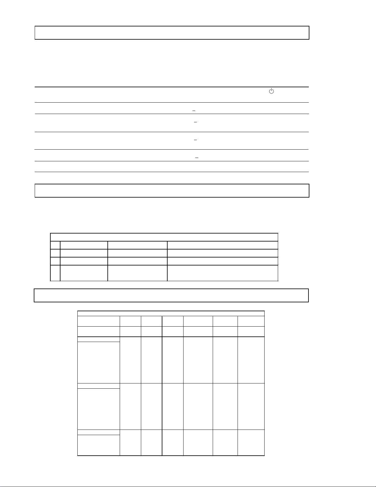
1 Normal operation active y es yes < 130 W -- Green
POWER MANAGEMENT
The power saving mode complies with the VESA Display P ower Management Signaling standard. Each
state of power management shall be activated by the host computer terminating the appropriate sync
signals. Blanking the video must precede ter mination of the sync signals. The elapsed time counter
shall also be controlled by the host computer . Reactivation of the monitor shall be accomplished from
the host computer by re-establishing the normal sync signal.
Power consumption Screen Horizontal Vertical Power Recovery time indicator
mode (video) sync signal sync signal consumption
2 Standby (1st mode) blank no yes < 15 W Approx. 3 sec. Green and Orange
3 Suspend (2nd mode) blank yes no < 15 W Approx. 3 sec. Green and Orange
4 Active-off (3rd mode) blank n o no < 3 W Approx. 10 sec. Orange
5 P ower-off -- -- -- 0 W -- Off
Alternate
Alternate
SELF DIAGNOSIS FUNCTION
When a failure occurs, the STANDBY/TIMER lamp will flash a set number of times to indicate the
possible cause of the problem. If there is more than one error, the lamp will identify the first of the
problem areas.
Status Area of Failure LED Indication
1 Failure 1 HV or +B Amber (0.5 second)/Off (0.5 second)
2 Failure 2 H Stop or V Stop Amber (1.5 second)/Off (0.5 second)
3 Failure 3 ABL Amber (0.5 second)/Off (1.5 second)
4 Aging/Self Test Amber (0.5 second)/Off (0.5 second)/
Green (0.5 second)/Off (0.5 second)
TIMING SPECIFICATION
TIMING SPECIF ICATION
Resolution (H x V) 640 x 480 720 x 400 800 x 600 1024 x 768 1280 x 1024 1600 x 1200
MODE
Dot Clock (MHz) 25.175 28.322 56.250 94.500 135.000 202.500
HORIZONTAL
Hor. Freq. (kHz) 31.469 31.469 53.674 68.677 79.976 93.750
H-Total 31.778 31.777 18.631 14.561 12.504 10.667
H-Blanking 6.356 6.355 4.409 3.725 3.022 2.765
H-Front Porch 0.636 0.636 0.569 0.50 8 0.119 0.316
H-Sync. 3.813 3.813 1.138 1.016 1.067 0.948
H-Back Porch 1.907 1.907 2.702 2.201 1.837 1.501
H-Active 25.422 25.422 14.222 10.836 9.481 7.901
(µsec.)
VERTICAL
Ver. Freq. (Hz) 59.940 70.087 85.061 84.997 75. 02 5 75.000
V-Total 525 449 631 808 1066 1250
V-Blanking454931 40 42 50
V-Front Porch1012 1 1 1 1
V-Sync. 2 2 3 3 3 3
V-Back Porch 33 35 27 36 38 46
V-Active 480 400 600 768 1024 1200
(lines)
SYNC.
Int (G)NoNoNo No No No
Ext (H/V)/Polarity Yes -/- Yes -/+ Yes +/+ Yes +/+ Yes +/+ Yes +/+
Ext (CS)/Polarity No No No No No No
Int/Non Int Non Int Non Int Non Int Non Int Non Int Non Int
123 4 5 6
Primary Mode
— 2 —
Page 3

TABLE OF CONTENTS
Section Title Page
Safety Check Out Instructions .............................................................. 4
1. GENERAL.................................................................................. 5
2. DISASSEMBLY
2-1. Cabinet Removal ........................................................... 9
2-2. Service Position ............................................................. 9
2-3. A and D Board Removal ............................................... 9
2-4. Picture Tube Removal ................................................. 10
CPD-2403
3. SAFETY RELATED ADJUSTMENTS ........................... 11
4. ADJUSTMENTS .................................................................... 12
5. DIAGRAMS
5-1. Block Diagram .............................................................. 15
5-2. Circuit Boards Location ................................................ 18
5-3. Schematic Diagrams and Printed Wiring Boards......... 18
1. D Board - Schematic Diagram ............................... 19
2. A Board - Schematic Diagram ............................... 26
5-4. Semiconductors ........................................................... 2 9
6. EXPLODED VIEWS
6-1. Chassis ........................................................................ 31
6-2. Packing Materials ........................................................ 3 2
7. ELECTRICAL PARTS LIST .............................................. 33
— 3 —
Page 4
CPD-2403
SAFETY CHECK-OUT
After correcting the original service problem, perform the
following safety checks before releasing the set to the
customer:
1. Check the area of y our repair f or unsoldered or poorlysoldered connections. Check the entire board surface
for solder splashes and bridges.
2. Check the interboard wiring to ensure that no wires are
“pinched” or contact high-wattage resistors.
3. Check that all control knobs, shields, covers, ground
straps, and mounting hardware hav e been replaced. Be
absolutely certain that you have replaced all the
insulators.
4. Look for unauthor ized replacement parts, particularly
transistors, that were installed during a previous repair .
Point them out to the customer and recommend their
replacement.
5. Look f or parts which, though functioning, show obvious
signs of deterioration. Point them out to the customer
and recommend their replacement.
6. Check the line cords for cracks and abrasion.
Recommend the replacement of any such line cord to
the customer.
7. Check the B+ and HV to see if they are specified v alues.
Make sure your instruments are accurate; be suspicious
of your HV meter if sets alwa ys have low HV.
8. Check the antenna terminals, metal trim, “metallized"
knobs, screws, and all other exposed metal parts for
AC Leakage. Check leakage as described below.
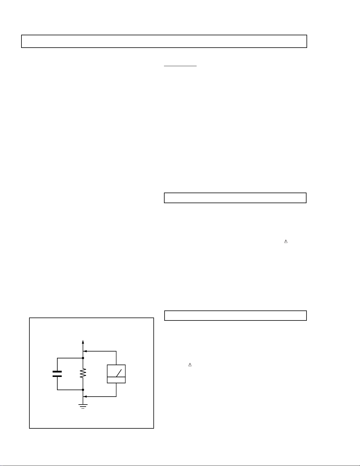
Leakage Test
The AC leakage from any exposed metal part to earth ground
and from all exposed metal parts to any exposed metal part
having a return to chassis, must not exceed 0.5 mA (500
microampere). Leakage current can be measured b y any one of
three methods.
1. A commercial leakage tester, such as the Simpson 229 or
RCA WT-540A. Follow the manuf acturers' instructions to use
these instructions.
2. A battery-operated AC milliammeter . The Data Precision 245
digital multimeter is suitable for this job.
3. Measuring the voltage drop across a resistor by means of
a VOM or battery-operated AC voltmeter. The "limit"
indication is 0.75 V, so analog meters m ust have an accura te
low voltage scale. The Simpson's 250 and Sanwa SH-63Trd
are examples of passive VOMs that are suitable. Nearly
all battery operated digital multimeters that have a 2V AC
range are suitable. (See Figure A)
WARNING!!
NEVER TURN ON THE POWER IN A CONDITION IN WHICH THE
DEGAUSS COIL HAS BEEN REMOVED.
SAFETY-RELA TED COMPONENT W ARNING!!
COMPONENTS IDENTIFIED BY SHADING AND MARK ON THE
SCHEMATIC DIA GRAMS, EXPLODED VIEWS AND IN THE P ARTS
LIST ARE CRITICAL FOR SAFE OPERATION. REPLACE THESE
COMPONENTS WITH SONY PARTS WHOSE PART NUMBERS
APPEAR AS SHOWN IN THIS MANUAL OR IN SUPPLEMENTS
PUBLISHED BY SONY. CIRCUIT ADJUSTMENTS THAT ARE
CRITICAL FOR SAFE OPERATION ARE IDENTIFIED IN THIS
MANUAL. FOLLOW THESE PROCEDURES WHENEVER CRITICAL
COMPONENTS ARE REPLACED OR IMPROPER OPERATION IS
SUSPECTED.
0.15 µF
To Exposed Metal
Parts on Set
1.5 k
Earth Ground
Figure A
AVER TISSEMENT!!
NE JAMAIS METTRE SOUS TENSION QUAND LA BOBINE DE
DEMAGNETISA TION EST ENLEVEE.
ATTENTION AUX COMPOSANTS RELATIFS A LA SECURITE!!
LES COMPOSANTS IDENTIFIES PAR UNE TRAME ET PAR UNE
Ω
AC
Voltmeter
(0.75 V)
MARQUE SUR LES SCHEMAS DE PRINCIPE, LES VUES
EXPLOSEES ET LES LISTES DE PIECES SONT D'UNE
IMPORTANCE CRITIQUE POUR LA SECURITE DU
FONCTIONNEMENT. NE LES REMPLACER QUE PAR DES
COMPOSANTS SONY DONT LE NUMERO DE PIECE EST
INDIQUE DANS LE PRESENT MANUEL OU DANS DES
SUPPLEMENTS PUBLIES PAR SONY. LES REGLAGES DE
CIRCUIT DONT L'IMPORTANCE EST CRITIQUE POUR LA
SECURITE DU FONCTIONNEMENT SONT IDENTIFIES DANS LE
PRESENT MANUEL. SUIVRE CES PROCEDURES LORS DE
CHAQUE REMPLACEMENT DE COMPOSANTS CRITIQUES, OU
LORSQU'UN MAUVAIS FONTIONNEMENT SUSPECTE.
— 4 —
Page 5
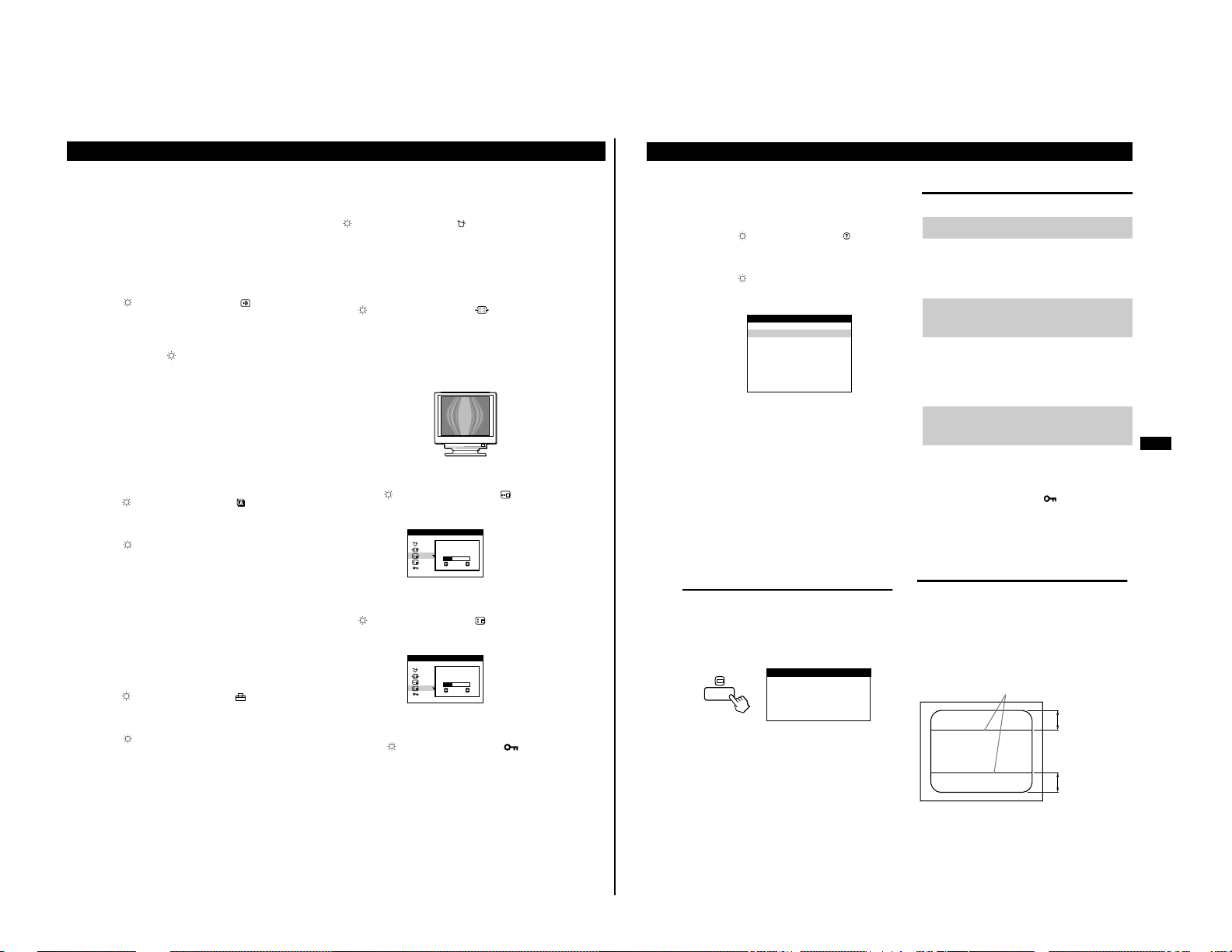
Getting Started
5
Getting Started Customizing Your Monitor
US
This monitor can be adjusted within the angles shown below. To
turn the monitor vertically or horizontally , hold it at the bott om with
both hands.
1
Press the (BRIGHTNESS)
v/V
or 6 (CONTRAST)
B/b
buttons.
The BRIGHTNESS/CONTRAST OSD appears.
2
To adjust the brightness.
Press the (BRIGHTNESS)
v/V
buttons.
To adjust the contrast.
Press the 6 (CONTRAST)
B/b
buttons.
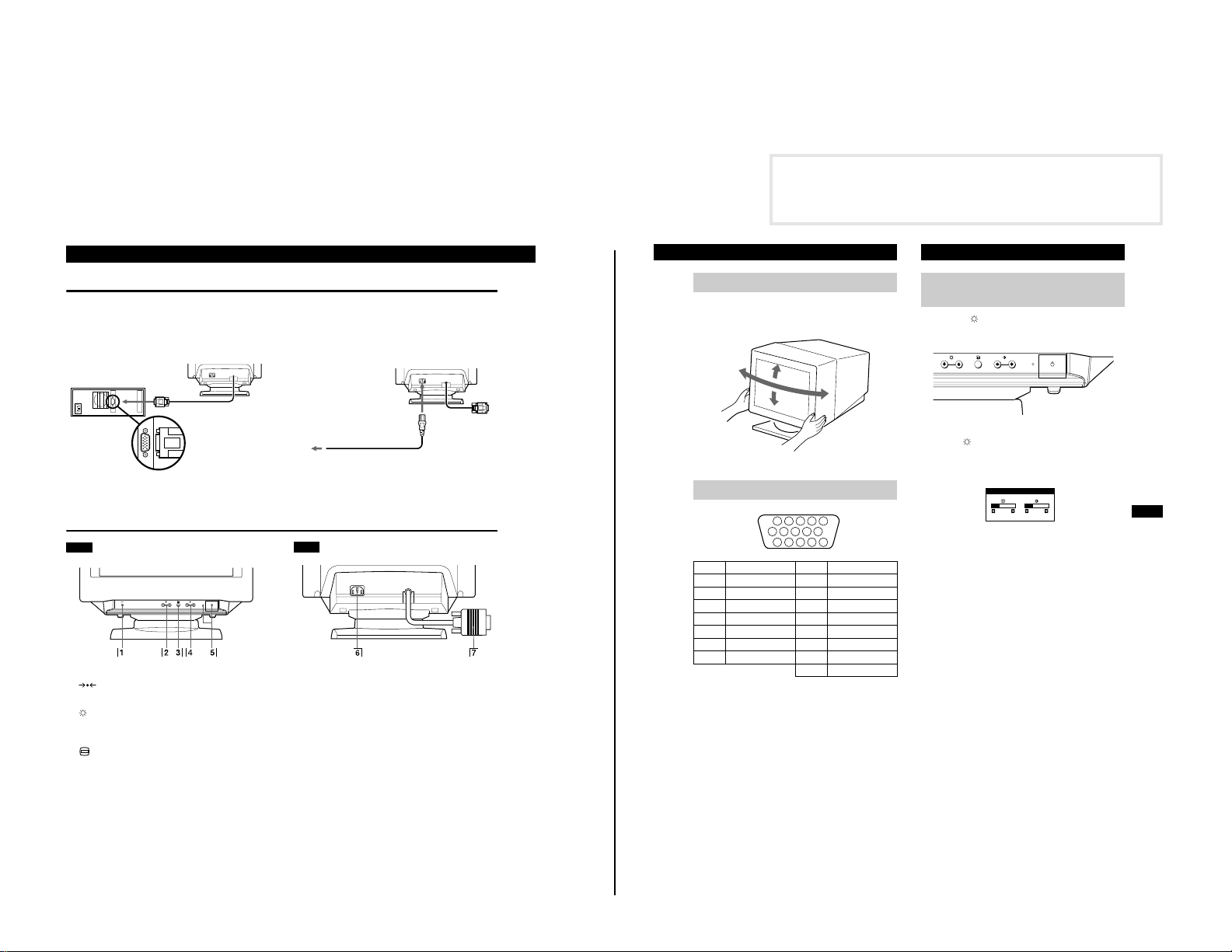
Use of the Tilt/Swivel
Video Connector
Pin No. Signal Pin No. Signal
1 Red video 8 Blue return
2 Green video 9 Not used (no pin)
3 Blue video 10 Ground
4 Ground 11 Ground
5 CPU host ground 12 SDA (serial data)
6 Red ground 13 Horizontal S ync
7 Green return 14 Vertical Sync
15 SCL (serial clock)
90°
5°
90°
15°
1234
5
987
10
11 12 13 14 15
6
Adjusting the Picture Brightness
and Contrast
Setup
Connect the monitor to your computer system.
This monitor will sync to platforms running at horizontal frequencies between 30 and 85 kHz.
Step 1
Make sure the computer system is switched off and attac h
the video signal cable to the video output of the computer.
Computer
to the video output
— 5 —
Parts and Controls
Front
(RESET) button (pages 6, 9)
1
This button resets the adjustments to the factory settings.
(BRIGHTNESS) (
2
These buttons adjust the picture brightness and function as the
v/V
(
) buttons when adjusting other items.
(MENU) button (page 6)
3
This button displays the MENU OSD.
(CONTRAST) (
4 6
These buttons adjust the contrast and function as the (
buttons when adjusting other items.
) buttons (page 5)
v/V
) buttons (page 5)
B/b
B/b
)
Step 2
Make sure the computer is switched off and attach the
power cord to the monitor. Then, attach the other end of
the power cord to a power outlet.
to a power outlet
Step 3
Switch on the monitor and computer.
Step 4
Adjust the user controls accord ing to your personal
preference.
Installation is complete.
Rear
(POWER) switch and indicator
5 1
This button turns the monitor on and off.
The indicator lights up green when the mo nitor is on , and ligh ts
up green and orange when the monitor is in Power Saving
mode.
AC IN connector
6
This connector provides AC power to the monitor.
Video input connector (HD15) (page 5)
7
This connector inputs RGB video signals and SYNC signals.
Power cord
SECTION 1
GENERAL
The following are partial abstracts from the Operating Instruction
Manual. The page numbers shown reflect those of the Operating
Instruction Manual.
BRIGHTNESS/CONTRAST
26 26
CPD-2403
4
Page 6
Customizing Your Monitor
7
Customizing Your Monitor
US
1
Adjusting the size and centering
of the picture (SIZE/CENTER)
This setting is stored in memory for the current input signal.
1
Press the MENU button.
The main MENU appears on the screen.
2
Press the
v/V
buttons to highlight SIZE/
CENTER and press the MENU button again.
The SIZE/CENTER menu appears on the screen.
3
Press the
v/V
buttons to select the desired
adjustment item. Then press the 6
B/b
buttons to
adjust the setting.
The OSD automatically disappears after about 30 seconds. To
close the OSD, press the MENU button again.
Note
Adjustment stops when either the horizonta l or ve rti cal size reaches its
maximum or minimum value.
2
Adjusting the shape of the
picture (GEOMETRY)
The GEOMETRY settings allow you to adjust the rotation and
shape of the picture.
The rotation setting is stored in memory for all input signals. All
other settings are stored in memory for the current input signal.
1
Press the MENU button.
The main MENU appears on the screen.
2
Press the
v/V
buttons to highlight GEOMETRY
and press the MENU button again.
The GEOMETRY menu appears on the screen.
3
First press the
v/V
buttons to select the desired
adjustment item. Then press the 6
B/b
buttons to
adjust the setting.
The OSD automatically disappears after about 30 seconds. To
close the OSD, press the MENU button again.
3
Adjusting the color of the picture
(COLOR)
The COLOR settings allow you to adjust the picture’s color
temperature by changing the color level of the whi te color field.
Colors appear reddish if the temperature is low, and bluish if the
temperature is high. This adjustment is useful for matching the
monitor’s colors to a printed picture’s colors.
This setting is stored in memory for all input signals.
1
Press the MENU button.
The main MENU appears on the screen.
2
Press the
v/V
buttons to highlight COLOR and
press the MENU button again.
The COLOR menu appears on the screen.
3
Press the
v/V
buttons to select a color
temperature.
The preset color temperatures are 9300K and 5000K. Since the
default setting is 9300K , the whites c hange fr om a bluish hue to
a reddish hue as the temperatur e is lowered to 5000K.
You can also fine tune the color temperature by selecting in
step 2 above, and using the 6
B/b
buttons to adjust the color
temperature manually.
This OSD allows you to adjust the color temperature between
9300K and 5000K.
Press the 6
B/b
buttons to adjust the color temperature.
The OSD automatically disappears after about 30 seconds. To
close the OSD, press the MENU button again.
Adjusting the Settings
Select To
HORIZONTAL CENTERING
shift the picture to the left or
right
VERTICAL CENTERING
shift the picture up or down
HORIZONTAL SIZING
enlarge or reduce the picture
width
VERTICAL SIZING
enlarge or reduce the picture
height
ZOOM
enlarge or reduce the picture
width and height
proportionally
Select To
ROTATION
rotate the picture
PINCUSHION
expand or contract the picture sides
PIN BALANCE
shift the picture sides to the left or right
KEYSTONE
adjust the picture width at the top of the
screen
KEY BALANCE
shift the picture to the left or r igh t a t the
top of the screen
The OSD (On-screen Display) System
Introducing the OSD System
You can adjust most of the monitor’s settings using the OSDs (Onscreen Display). All of the OSDs in this illustration are described on
the following pages in order. You can access any of these OSDs
from the MENU OSD. To adjust monitor settings using the OSDs,
follow the steps below:
Basic controls:
• Use the (MENU) button to display the MENU OSD and to
select menu items .
• Use the (BRIGHTNESS)
items and to adjust settings.
To adjust the monitor settings:
1
Press the MENU button to display the MENU OSD.
2
Highlight the desired OSD using the BRIGH TNESS butto ns and
press the MENU button again.
— 6 —
1
4
7
6
SIZE/CENTER
SIZE/CENTER
26
CONVERGENCE
CONVERGENCE
26
HELP
HELP
RETURN TO MAIN MENU
RECOMMENDED RESOLUTION
FLICKER
THIN HORIZONTAL LINE
DISTORTED SHAPE
OUT OF FOCUS
DISCOLORATION
v/V
buttons to highlight menu
Resolution for current
input signal
1
2
3
4
5
6
7
GEOMETRY
2
GEOMETRY
LANGUAGE
5
LANGUAGE
ENGLISH
FRANÇAIS
DEUTSCH
ESPAÑOL
ITALIANO
NEDERLANDS
SVENSKA
MENU
26
3
If necessary, use the BRIGHTNESS buttons to select a specific
item.
4
Adjust the monitor setting using the BRIGHTNESS and
CONTRAST buttons.
• To reset the current item to its original setting, press the
(RESET) button while the item’s adjustment OSD is displayed.
5
When you finish adjusting the setting, press the MENU button to
return to the MENU OSD.
Press the MENU button twice to return to norma l viewing.
• Resetting: If you press the RESET button while an OSD is
displayed, only the current adjustment item is reset. For
additional information on using the reset function, see the
“Resetting the Adjustments” section on page 9.
• Each of the adjustment’s OSD automatically disappears after
30 seconds.
EXIT
SIZE/CENTER
GEOMETRY
COLOR
CONVERGENCE
LANGUAGE
OPTION
HELP
80.0kHz/ 75Hz
1280 X 1024
MENU
OK
Horizontal/Vertical
frequencies for
current input signal
COLOR
3
COLOR
9300K
5000K
OPTION
6
OPTION
DEGAUSS
ON
COLOR
9300K
5000K
CPD-2403
26
Page 7
Customizing Your Monitor
9
Customizing Your Monitor
US
7
Using the HELP OSD
1
Press the MENU button.
The main MENU appears on the screen.
2
Press the
v/V
buttons to highlight HELP and
press the MENU button again.
The HELP OSD appears on the screen.
3
Press the
v/V
to select an option from the HELP
menu, then press the MENU button to view the HELP
information.
Resetting the adjustments
Navigate through the on-screen menus to select the adjustment item
you want to reset, and press the RESET button before the OSD
disappears.
Press the RESET button when no OSD is displayed on the screen.
Note that the following items are not reset by this method:
• o n-screen menu language (page 8)
• on-screen menu position (page 8)
Press and hold the reset button for more than two seconds. This
resets everything to the factory presets including the input selectio n.
Note
The RESET button does not function when
(CONTROL LOCK) is
set to ON.
HELP
RETURN TO MAIN MENU
RECOMMENDED RESOLUTION
FLICKER
THIN HORIZONTAL LINE
DISTORTED SHAPE
OUT OF FOCUS
DISCOLORATION
Resetting a specific adjustment
Resetting all of the adjustments
for the current input signal
Resetting all of the adjustment
data to the factory presets
Design and specifications are subject to change without notice.
Monitor Information
You can display the model name, serial number and year of
manufacture using the INFORMATION OSD.
Press and hold the MENU button for 5 seconds.
The INFORMATION OSD appears.
The INFORMATION OSD includes the model name, serial number
and year of manufacture.
The OSD automatically disappears after about 30 seconds.
If Thin Lines Appear on Your
Screen (damper wires)
The lines you may be seeing on your screen are normal for the
Trinitron monitor and are not a malfunction. These are shadows
from the damper wires that stabilize the aperture grille, and are most
noticeable when the screen’s background is light (usually white).
The aperture grille is the essential element that makes a Trinitron
picture tube unique by allowing more light to re ach the screen,
resulting in a brighter, more detailed picture.
INFORMATION
MODEL : CPD–24****
MANUFACTURED : 1999–53
SER NO : 1234567
Damper wires
Approx. 6 cm
Approx. 6 cm
Adjusting the quality of the
4
picture (CONVERGENCE)
The CONVERGENCE settings allow you to adjust the quality of
the picture by eliminating red or blue shadows around letters,
characters and lines.
Both settings are stored in memory for all input signals.
1
Press the MENU button.
The main MENU appears on the screen.
2
Press the
CONVERGENCE and press the MENU button again.
The CONVERGENCE menu appears on the screen.
3
Press the 6
convergence, or the
vertical convergence.
The OSD automatically disappears after about 30 seconds. To
close the OSD, press the MENU button again.
Changing the OSD language
5
(LANGUAGE)
This setting is stored in memory for the current input signal.
1
Press the MENU button.
— 7 —
The main MENU appears on the screen.
2
Press the
and press the MENU button again.
The LANGUAGE menu appears on the screen.
3
Press the
prefer.
The OSD automatically disappears after about 30 seconds. To
close the OSD, press the MENU button again.
Additional settings (OPTION)
6
You can manually degauss (demagnetize) the screen, cancel the
moire, adjust the OSD horizontal position, adjust the OSD vertical
position and lock the controls using the OPTION OSD.
1
Press the MENU button.
The main MENU appears on the screen.
2
Press the
press the MENU button again.
The OPTION menu appears on the screen.
3
Press the
adjustment item.
Adjust the selected item according to the following instructions.
The OSD automatically disappears after about 30 seconds. To
close the OSD, press the MENU button again.
8
buttons to highlight
v/V
buttons to adjust the horizontal
B/b
buttons to highlight LANGUAGE
v/V
v/V
buttons to highlight OPTION and
v/V
v/V
buttons to adjust the
v/V
buttons to select the language you
buttons to highlight the desired
Degaussing the monitor
The monitor is automatically degaussed (demagnetized) when the
power is turned on.
To manually degauss the monitor, first press the
buttons to highlight (MANUAL DEGAUSS).
v/V
Then press only the right 6 b button.
The monitor is degaussed for about three seconds. If a second
degauss cycle is needed, allow a minimum interval of 20
minutes for the best result.
Adjusting the amount of the moire cancellation
To adjust the amount of moire cancellation, first press
the
buttons to highlight ( MOIRE
v/V
CANCEL). Then press the
amount of moire cancellation until the moire effect is
at a minimum.
* Moire is a type of natural interference which produces soft, wavy lines on
your screen. It may appear due to interference between the pattern of the
picture on the screen and the phosphor pitch pattern of the monitor.
Example of moire
buttons to adjust the
6 B/b
Adjusting the OSD Horizontal Position
To change the horizontal position of the OSD, first
press the
POSITION). Then press the
the horizontal position of the OSD.
buttons to highlight (OSD H
v/V
OPTION
OSD H
POSITION
6 B/b
26
buttons to adjust
Adjusting the OSD Vertical Position
To change the vertical position of the OSD, first press
the
buttons to highlight (OSD V
v/V
POSITION). Then press the
the vertical position of the OSD.
OPTION
Locking the controls
To protect adjustment data by locking the controls,
first press
(CONTROL LOCK). Then press the
toggle the Control Lock on or off.
Only the 1 (power) switch and MENU button will operate.
buttons to highlight
v/V
OSD V
POSITION
6 B/b
26
buttons to adjust
6 B/b
buttons to
CPD-2403
Page 8

Additional Information
12
Additional Information
* If a second degauss cycle is needed, allow a minimum interval of 20 minutes for the best result. A humming noise may be heard, but this is not a malfunction.
Picture is fuzzy
• Adjust the brightness and contrast (page 5).
• Degauss the monitor* (page 8).
• If CANCEL MOIRE is ON, the picture may become fuzzy. Decrease the moire cancellation
effect (page 8) or set CANCEL MOIRE to OFF.
Picture is ghosting
• Eliminate the use of video cable extensions and/or video switch boxes.
• Check that all plugs are firmly seated in their sockets.
Picture is not centered or sized
properly
• Adjust the size (page 7) or centering (page 7). Note that some video modes do not fill the
screen to the edges.
Edges of the image are curved
• Adjust the geometry (page 7).
Wavy or elliptical pattern (moire) is
visible
• Can cel the moire (page 8).
x
Problems caused by the connected computer or other equipment
• Change your desktop pattern.
Color is not uniform
• Degauss the monitor* (page 8). If you place equipment that generates a magnetic field, such
as a speaker, near the monitor, or if you change the direction the monitor faces, color may
lose uniformity.
White does not look white
• Adjust the color temperature (page 7).
Letters and lines show red or blue
shadows at the edges
• Ad just the convergence (page 8).
Monitor buttons do not operate
• If the control lock is set to ON, set it to OFF (page 8).
A hum is heard right after the
power is turned on
• This is the normal sound of the auto-degauss cycle. When the power is turned on, the monitor
is automatically degaussed for 3 seconds.
Symptom Check these items
Warning Messages
If there is something wrong with the input signal, one of the following messages appears.
Out of Scan Range
1
This message indicates that the current input signal is not appropriate for the monitor’s specificatons.
Power Save Mode
2
This message indicates that the monitor has reduced power consumption.
Check Signal Cable (self test pattern)
3
This message indicates that either no input sig nal is received, or the video cable is not connected.
To solve these problems, see the “Troubleshooting” section below.
Troubleshooting
— 8 —
If the problem is caused by the connected computer or other equipment, please refer to the connected equip ment’s instruction manual.
Symptom Check these items
No picture
If the 1 (power) indicator is not lit • Check that the power cord is properly connected.
If the CHECK SIGNAL CABLE
message appears on the screen, or if
the 1 (power) indicator is either
orange or alternating between green
and orange
If the OUT OF SCAN RANGE
message appears on the screen
Picture flickers, bounces,
oscillates, or is scrambled
• Check that the 1 (power) switch is in the “on” position.
• Check that the video signal cable is properly connect ed and all plugs are firmly seated in
their sockets.
• Check that the HD15 video input cable’s pins are not bent or pushed in.
Problems caused by the connected computer or other equipment
x
• The computer is in power saving mode. Try pressing any key on the computer keyboard.
• Check that the computer’s power is “on.”
• Check that the graphic video board is completely seated in the proper bus slot.
Problems caused by the connected computer or other equipment
x
• Check that the video frequency range is within that specified for the monitor. If you replaced
an old monitor with this monitor, rec onnect the o ld monitor and adjust the freque ncy ra nge to
the following:
Horizontal: 30 – 85 kHz
V e rtic a l: 48 – 120 H z
• Isola te and eliminate any potential source s of electric or magnetic fields such as other
monitors, laser printers, electric fans, fluorescent lighting and televisions.
• Move the monitor away from power lines or place a magnetic shield near the monitor.
• Try plugging the monitor into a different AC outlet, prefera bly on a dif fe re nt circ uit .
• Try turning the monitor 90° to the left or right.
Problems caused by the connected computer or other equipment
x
• Check your graphic video board manual for the proper monitor setting.
• Confirm that the graphics mode (VESA, VGA, etc.) and the frequency of the input signal are
supported by this monitor (Appendix). Even if the frequency is within the proper range,
some graphic video boards may have a sync pulse that is too narrow for the monitor to sync
correctly.
• Adjust the computer’s refresh rate (vertical frequency) to obtain the best possible picture.
INFORMATION
MONITOR IS WORKING
OUT OF SCAN RANGE
CHANGE PC SETTING
INFORMATION
MONITOR IS IN
POWER SAVE MODE
ACTIVATE USING PC
INFORMATION
MONITOR IS WORKING
CHECK SIGNAL CABLE
WHITE
RED
GREEN
BLUE
CPD-2403
US
11
Page 9
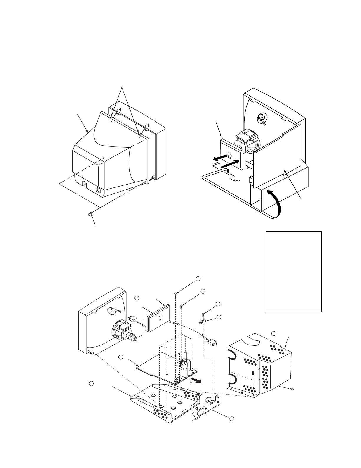
SECTION 2
DISASSEMBLY
CPD-2403
2-1. CABINET REMOVAL
2-2. SERVICE POSITION
Two claws
Cabinet
PUSH
PUSH
Two screws
(BVTP 4 x 16)
2-3. A and D BOARD REMOVAL
1
A board
A board
2
Two screws
(BVTP 3 x 12)
3
Five screws
(BVTP 3 x 8)
4
One screw
5
Cable stopper
(BVTT 4 x 8)
D board
1 When the D-board is
placed in service
position, the Safety Earth
Wire (green and yellow
wire) is disconnected.
2 After service is
completed and the
D-board reinstalled, the
Safety Earth Wire must
be reattached to the
chassis with the proper
screw. This must be
confirmed before any
subsequent procedures
are attempted.
7
Chassis base
D board
8
— 9 —
10
Holder
7
EMI Shield
Page 10

CPD-2403
Anode Button
c
2-4. PICTURE TUBE REMOVAL
WARNING:
BEFORE REMOVING
THE ANODE CAP
High voltage remains in the CRT even
after the power is disconnected. T o
avoid electric shock, discharge CR T
before attempting to remove the anode
cap. Short between anode and CRT
coated earth ground strap.
Coated Earth
Ground Strap
8
Demagnetization coil
7
Tension spring
6
A board
5
Neck assy
4
Deflection yoke
3
Four screws
(Tapping screw 5)
Picture tube shield
2
1
Anode cap
9
Two screws
(BVTP 4 x 16)
10
Stand
ass'y
(D board)
Cushion
ANODE CAP REMOVAL
WARNING: High voltage remains in the CRT ev en after the power is disconnected. To avoid electric shock, discharge CRT
NO TE: After remo ving the anode, shor t circuit the anode of the picture tube and the anode cap to either the metal
before attempting to remove the anode cap. Short between anode and CRT coated earth ground strap.
chassis , CRT shield, or carbon painted on the CRT.
REMOVAL PROCEDURES
a
1 Turn up one side of the rubber cap in
the direction indicated by arrow a .
2 Use your thumb to pull the rubber
HOW TO HANDLE AN ANODE-CAP
1 Do not use sharp objects which may cause damage to the
surface of the anode cap.
2 Do not squeeze the rubber covering too hard to avoid damag-
ing the anode cap. A mater ial fitting called a shatter-hook terminal is built into the rubber.
3 Do not force turn the foot of the rubber cover. This may cause
the shatter-hook terminal to protrude and damage the rubber.
b
cap firmly in the direction indicated
by arrow b .
3 When one side of the rubber cap
separates from the anode button,
the anode cap can be removed by
turning the rubber cap and pulling
it in the direction of arrow c .
— 10 —
Page 11

SECTION 3
SAFETY RELATED ADJUSTMENTS
CPD-2403
When replacing parts shown in the table below, the
following operational checks must be performed as a
safety precaution against X-ray emissions from the unit.
Part Replaced ( )
HV ADJ
HV Regulator
Circuit
HV HOLD
DOWN Circuit
Beam Current
Protector Circuit
Allow the unit to warm up for one minute prior to checking
the following conditions:
D board T501, IC501, RV501, R540,
D board T501, R510, R543, R547,
D board T501, R545, R546, R548,
R V501
Part Replaced ( )
R541, R542, R544, R564, R567,
R568, C532, C534, C539, C553,
C554, C555, C556, C558, C561
R549, R552, R595, D515,
D517, C540, C542, C544,
IC607, IC901
R550, R596, R934, C535,
C541, IC605, IC607, IC901
a) HV Regulator Check
1) Input white cross hatch signal. (fH = 80 kHz)
2) CONT maximum and BRT center
3) Cut off Screen VR (G2).
4) Input voltage: 120 ± 2 V AC
5) Confirm that the voltage is within the voltage range
shown below.
Standard voltage: 26.9 KV ± 0.4 KV
6) When replacing components identified by , make
sure to recheck the High Voltage.
7) V erify the High V oltage as shown above (26.9 KV ± 0.4 KV)
is within specification. If not, set H. SIZE data at
minimum (-127) and then adjust RV501 on "D" Board.
8) After adjusting the High Voltage within specification,
put the R V cover on R V501 as shown below and apply
sufficient amount of R TV around RV501.
b) HV Protector Circuit Check
1) Confirm that the voltage between cathode of D517 an
GND is more than 27.5 VDC.
2) Using an external DC Power supply, apply the voltage
shown below between cathode of D517 on "D" and GND,
and confirm that the HV Hold-Down circuit works. (Raster
disappears) Apply DC V oltage: Less than 35.5 VDC
Check Condition
• Input voltage : 120 ± 2 VAC
• Input signal : (fH = 69 kHz), White Cross Hatch
• Controls : CONT (max) & BR T (center)
• B+ Voltage : 179 ± 3.0 VDC
c) Beam Protector Check (Software logic)
1) Using an external current source, apply < 1.55mA between
of FBT (T501) and GND, and confirm that the
pin
raster fades out.
Check Condition
• Input voltage : 120 ± 2 V AC
• Input signal : (fH = 80 kHz), White Cross Hatch
• Controls : CONT (max) & BRT (min)
d) B+ V oltage Check
1) Input white cross hatch (fH = 80 kHz) signal.
2) CONT (max) & BRT (center)
3) Input voltage: 120 ± 2 VAC
Note: Use NF power supply or make sure that
distortion factor is 3% or less.
4) Confirm that the voltage is within the voltage
range shown below.
Standard voltage: 179 ± 3.0 VDC
RV501
— 11 —
Page 12

CPD-2403
SECTION 4
ADJUSTMENTS
Connect the communication cable of the connector located on the D board on the monitor. Run the service software and then follo w the
instructions.
1-690-391-211A-1500-819-A
IBM AT Computer
as a Jig
D-sub
(9 Pin [female])
*The parts above ( ~ ) are necessary for DAS adjustment.
mini Din
(8Pin)
1
2
Interface Unit
3
4 Pin
4 Pin 4 Pin
Allow a 30 minute warm-up period prior to making the following adjustments:
4-1. Landing Rough Adjustment
1. Display the all white pattern.
2. Adjust the contrast to maximum value.
3. Display the plain green pattern.
4. Slide the DY back and roughly adjust the plain green
pattern with the purity magnet so that it is centered on
the screen.
4-3. Co nvergence Rough Adjustment
5. Moving the DY forward, adjust so that an entire screen
becomes pure green.
6. Adjust the tilt of DY and tighten lightly with a clamp.
3-702-691-01
3
Connector Attachment
To BUS CONNECTOR
12. If the corner landing is out of specification, use a disk
magnet for the landing correction.
13. If disk magnets were used, perform an auto degauss.
14. Remove the wobbling coil and sensor .
15. Fix the purity magnet on DY with white paint.
1. Enter the white crosshatch signal.
2. Roughly adjust the horizontal (H.ST AT) and vertical
(V.STAT) convergence at four-pole magnet.
3. Roughly adjust HMC and VMC at six-pole magnet.
4-2. Landing Fine Adjustment
1. Place the monitor in the Helmholtz coil.
2. Set TLH plate to zero position.
3. Display plain green pattern.
4. Degauss CRT face and iron parts with degauss equipment or
hand-degausser.
5. Perform auto degauss.
6. Attach a wobbling coil to the specified position of CRT neck.
7. Put the sensor of landing checker to CRT face.
8. Adjust purity, DY position and DY tilt.
9. Tighten DY screw.
10. Perform auto degauss.
11. Adjust top and bottom pin by pitching DY up and down with
two wedges so that [a] is equal to [b].
4-4.
Convergence and V. Key (H. Trp) Fine Adjustment
Neck Ass'y
A Board
6-pole
Mg
H-Trp VR
Purity
Magnet
4-pole
Mg
TLV VR
DY
YCV VR
TLH Plate
XCV VR
CRT
1. Display crosshatch pattern with green lines and black
field.
2. Adjust V . Key (=H. Trapezoid) with H-T rp VR so that [a]
is equal to [b].
3. Change "CONV_OFF_NDX" to "7".
— 12 —
Page 13

CPD-2403
4. Display crosshatch pattern with red and blue lines and
black field.
5. Adjust H.STAT and V.STAT with 4 pole magnet. Use 4
pole magnet, not "HSTAT" and "VSTAT".
4 Pole Magnet
6. Display crosshatch pattern with white lines and black field.
7. Adjust HMC and VMC with 6 pole magnet.
6 Pole Magnet
8. Display crosshatch pattern with red and blue lines and
black field.
9. If necessary, repeat steps 5-8.
10. Change "CONV_OFF_NDX" to "3".
11. Adjust H.TIL T with TLH plate.
TLH movement
R B B R
14. Adjust V.TILT with TLV VR.
TL V movement
15. If necessary, repeat steps 3-14 to make the
optimum condition for the entire screen.
16. Fix 4-pole magnet, 6-pole magnet and XCV
VR with white paint
Zero Position NECK Ass'y
4-5. Vertical and Horizontal Position and
Size Specification
a
fH > 60kHz fH < 60kHz
a = 2.0 mm 2.4 mm
b = 2.0 mm 2.4 mm
A
B
b
A B
234 312
4-6. Focus adjustment
Adjust focus (V) and focus (H) for optimum focus.
12. Adjust XCV with XCV VR.
XCV movement
13. Adjust YCH with YCH VR.
YCH movement
RB
Focus (V)
Focus (H)
FBT
— 13 —
Page 14

CPD-2403
4-7. Digital Convergence Adjustment
Convergence (Low) Mode
1. Adjust the H.STAT and V .ST AT with "HST A T" and
"VST A T".
A. Horizontal Convergence
Adjust each misconvergence point in sequence.
YBH-T-LO
CBH-T-L-LO
MBH-T-L-LO
APH-L-LO
MBH-B-L-LO
CBH-B-L-LO
9
17
1
19
11
5
HSTAT
6
YBH-B-LO
10
18
2
20
12
B. Vertical Convergence
V STAT-T-LO
CCV-T-L-LO
MCV-T-L-LO
XBV-L-LO
MCV-B-L-LO
CCV-B-L-LO
13
21
3
23
15
7
VSTAT
8
V STAT-B-LO
CBH-T-R-LO
MBH-T-R-LO
APH-R-LO
MBH-B-R-LO
CBH-B-R-LO
14
CCV-T-R-LO
22
MCV-T-R-LO
4
XBV-R-LO
24
MCV-B-R-LO
16
CCV-B-R-LO
Vertical Convergence
V STAT-T-HI
CCV-T-L-HI
MCV-T-L-HI
XBV-L-HI
MCV-B-L-HI
CCV-B-L-HI
13
21
3
23
15
7
VSTAT-HI
8
V STAT-B-HI
14
22
4
24
16
Adjust each misconvergence point in sequence.
2. Repeat the procedure of A and B so that the convergence of the entire screen is within the specification.
4-8.Convergence Specification
C
B
A
312 mm
A Zone:
Primary Mode Others
H: < 0.25mm H: < 0.3mm
234 mm
V: < 0.2mm V: < 0.3mm
B Zone:
Primary Mode Others
H: < 0.3mm H: < 0.4mm
V: < 0.3mm V: < 0.4mm
C Zone:
Primary Mode Others
H: < 0.35mm H: < 0.4mm
V: < 0.35mm V: < 0.4mm
CCV-T-R-HI
MCV-T-R-HI
XBV-R-HI
MCV-B-R-HI
CCV-B-R-HI
Adjust each misconvergence point in sequence.
2. Repeat the procedure of A and B so that the convergence of the entire screen is within the specification.
Convergence (High) Mode
1. Adjust the H.STAT and V .ST AT with "HST A T-HI" and
"VST A T-HI".
Horizontal Convergence
CBH-T-L-HI
MBH-T-L-HI
APH-L-HI
MBH-B-L-HI
CBH-B-L-HI
YBH-T-HI
9
17
1
19
11
5
HSTAT-HI
6
YBH-B-HI
10
CBH-T-R-HI
18
MBH-T-R-HI
2
APH-R-HI
20
MBH-B-R-HI
12
CBH-B-R-HI
Adjust each misconvergence point in sequence.
— 14 —
Page 15

5-1. BLOCK DIAGRAM
SECTION 5
DIAGRAMS
CPD-2403
5-2. CIRCUIT BOARDS LOCATION
5-3. SCHEMATIC DIAGRAMS AND PRINTED WIRING BOARDS
Note:
• All capacitors are in µF unless otherwise noted. pF: µµF
50 WV or less are not indicated except for electro lytic.
• Indication of resistance, which does not have one for
rating electrical power, is as follows.
Pitch: 5 mm
Rating electrical power 1/4 W (CHIP: 1/10 W)
• When replacing parts shown in the table below, be sure to
perform the safety related adjustment.
HV ADJ
Part Replaced ( )
R V501
• All resistors are in ohms.
• : nonflammable resistor.
•
•
: fusible resistor.
: internal component.
• : panel designation and adjustment for repair.
• All variable and adjustable resistors have characteristic curve
B, unless otherwise noted.
•
: earth-ground
•
: earth-chassis.
• The components identified by in this basic schematic
diagram have been carefully factory-selected for each set in
order to satisfy regulations regarding X-ray radiation.
Should replacement be required, replace only with the
value originally used.
• When replacing components identified by
necessary adjustments by using RV501 (
, make the
) as indicated.
(See page 11)
Note: The components identified by shading and
mark are critical for safety. Replace only with
part number specified.
Note: Les composants identifies per un trame et une
marque sont critiques pour la securite. Ne les
remplacer que par une piece portant le numero specifie.
Part Replaced ( )
HV Regulator
Circuit
HV HOLD
DOWN Circuit
Beam Current
Protector Circuit
D board T501, IC501, RV501, R540,
R541, R542, R544, R564, R567,
R568, C532, C534, C539, C553,
C554, C555, C556, C558, C561
D board T501, R510, R543, R547, R549,
R552, R595, D515, D517, C540,
C542, C544, IC607, IC901
D board T501, R545, R546, R548, R550,
R596, R934, C535, C541,
IC605, IC607, IC901
• All voltages are in volts.
• Readings are taken with a 10 ΜΩ digital multimeter
• Readings are taken with a color-bar signal input.
• Voltage variations may be noted due to normal production
tolerances.
• * : Cannot be measured.
• Circled numbers are waveform references.
•
•
: B +bus.
: B - bus.
852 Block Diagram.p65 8/17/99, 1:23 PM1
— 15 — — 16 — — 17 — — 18 —
Page 16

CPD-2403
1
2 3
5.1 Vp-p (H) 3.5 Vp-p (H)
5.5 Vp-p (H)
4 5
6
6.0 Vp-p (H)
1.175 kVp-p (H)
47.5 Vp-p (H)
7 8
9
1.8 Vp-p (H) 55.3 Vp-p (H) 12.0 Vp-p (H)
D BOARD WAVEFORMS
10 11
12
10.5 Vp-p (H) 9.3 Vp-p (H) 12.0 Vp-p (H)
13 14 15
1.5 Vp-p (H) 1.181 kVp-p (H) 1.7 Vp-p (H)
D BOARD SCHEMATIC DIAGRAM
D BOARD IC VOLTAGE LIST
IC401 IC502 IC603
pin volt pin volt pin volt 8 5.0 pin volt 37 4.0 15 GND
1 1.6 1 1.4 1 9.2 9 4.9 1 NC 38 5.0 16 11.5
2 14.8 2 1.4 2 8.1 10 11.9 2 5.0 39 5.0 17 0.4
3 -14.6 3 -15.0 3 NC 11 4.5 3 2.5 40 NC 18 5.6
4 -15.1 4 0.1 4 3.5 12 4.9 4 2.2 41 NC 19 10.4
5 0.2 5 14.8 5 3.5 13 5.0 5 NC 42 NC 20 9.2
6 14.8
7 1.6 pin volt
IC501
pin volt 2 88.6 1 2.5 17 4.6 9 NC 46 1.2 24 4.9
1 11.9 3 79.3 2 GND 18 GND 10 GND 47 0.6 25 3.5
2 4.0 4 88.7 3 7.0
3 4.0 5 98.4
4 5.5
5 8.9 pin volt IN 14.8 2 2.5 14 4.7 51 4.9 29 0.4
6 4.5 1 153.5 OUT 11.9 3 2.5 15 4.9 52 4.9 30 GND
7 GND 2 NC GND GND 4 2.5 16 3.9 53 5.0
8 0.2 3 GND 4 4.8 5 2.5 17 2.3 54 4.9 pin volt
9 GND 4 2.5
10 8.2 5 0.0 pin volt 7 -15.0 19 0 56 GND 2 GND
11 4.4 6 12.5 IN 9.5 8 GND 20 0.1
12 5.8 7 12.3 OUT 5.0 9 14.8 21 5.0 pin volt 4 4.9
13 5.8 8 2.5 GND GND 10 NC 22 0.2 1 2.2 5 5.0
14 5.8 9 2.8
15 5.2 10 NC pin volt 12 GND 24 5.0 3 4.0 pin volt
16 11.3 11 GND IN 11.9
17 11.9 12 NC OUT 5.0 pin volt 26 0 5 GND 2 GND
18 6.8 13 0.9 GND GND 1 -0.2 27 0.5 6 4.0 3 GND
19 8.0 14 6.1
20 6.1
21 GND pin volt 1 4.9 4 3.8 30 0.5 9 4.0 6 4.6
22 4.3 1 3.1 2 5.0 5 -15.0 31 5.0 10 5.0 7 5.0
23 4.0 2 9.1 3 4.9 6 3.8 32 0.9 11 6.2 8 5.0
24 4.0 3 GND 4 4.9 7 3.8 33 0.4 12 4.7
IC503
1 89.5 pin volt 16 4.0 8 NC 45 2.3 23 5.0
IC601
IC602
4 6.3 5 5.0 8 -0.2 34 4.7 13 NC
5 1.2 6 5.0 9 -0.2 35 4.7
6 12.3 14 3.3 6 4.8 43 NC 21 2.4
IC604
IC605
pin volt 1 -0.2 13 NC 50 0.4 28 0
IC607
IC608
IC701
pin volt 3 3.8 29 GND 8 4.9 5 4.0
7 5.0
15 1.1 7 0 44 2.3 22 9.7
IC702
pin volt 12 NC 49 0.4 27 4.9
6 -0.1 18 3.7 55 NC 1 GND
11 3.2 23 4.7 2 4.7
IC703
2 -0.2 28 2.8 7 5.6 4 GND
10 14.8
IC901
11 5.1 48 3.7 26 0.5
25 0 4 4.6 1 GND
36 4.6 14 0.9
IC904
IC902
3 GND
IC905
All voltages are in V
Schematic diagrams
Block diagram
D
board
D BOARD TRANSISTOR VOLTAGE LIST
BCE
Q501 5.5 11.5 5.5
Q502 5.5 GND 5.5
Q504 1.1 135.0 0.6
Q505 0.6 -15.1 1.1
Q506 2.2 GND 2.8
Q507 -0.6 49.1 GND
Q508 0.5 11.9 0.9
Q518 2.3 88.5 2.8
Q519 0.4 11.8 GND
Q521 4.8 GND 5.4
Q522 4.7 GND 5.0
Q524 5.0 GND 5.5
Q525 0.5 11.9 0.9
Q601 0 11.9 GND
Q603 5.0 0 GND
Q604 0 8.1 GND
Q605 4.8 0 GND
Q903 0.4 5.5 GND
All voltages are in V
D BOARD TRANSISTOR
VOLTAGE LIST
DGS
Q503 93.0 176.0 179.0
Q510 84.5 7.9 GND
Q511 -11.1 -1.8 -14.8
Q512 0 4.9 GND
Q513 33.2 0.4 GND
Q514 33.8 0.4 GND
Q515 0 4.9 GND
Q516 0 5.0 GND
Q520 88.9 176.0 179.0
Q602 131.8 2.4 0.1
All voltages are in V
— 20 — — 21 — — 22 —— 19 —
FOLDOUTD.p65 8/17/99, 10:38 AM2
Page 17

D
NOTE:
Portions of this circuit marked as shown are high
voltage areas. Use care to prevent electric shocks
during inspection or repair.
[ POWER DEFLECTION ]
CPD-2403
1
2345678910111213
A
D BOARD LOCATOR LIST
B
C
D
E
DIODE
D401 F-9 D518 G-7 D611 E-10 D907 G-3 D927
D402 F-10 D519 G-7 D612 E-10 D908 H-3 D928
D403 F-10 D520 G-11 D613 E-9 D909 J-4 D929
D404 F-10 D521 G-11 D614 D-8 D910 J-4 D930 H-3 IC607 E-3 Q512 I-3
D501 I-5 D522 J-2 D615 D-7 D911 H-3 D931 I-2 IC608 E-5 Q513 I-3
D502 I-8 D523 J-2 D616 D-7 D913 F-4 D932 I-2 IC701 B-3 Q514 I-3
D504 F-11 D524 H-10 D617 D-9 D914 H-3 D933 I-2 IC702 C-5 Q515 I-3
D505 H-8 D525 H-10 D618 E-8 D915 J-4 D934 I-2 IC703 B-4 Q516 I-3
D506 I-9 D527 F-10 D619 D-7 D916 H-3 D935 E- 2 IC901 H-3 Q518 G-5
D507 G-4 D601 D-11 D620 B-7 D917
D509 F-13 D602 E- 13 D621 E-10 D918
D510 F-11 D603 D-6 D622 E- 7 D919
D511 F-5 D604 B- 6 D704 C-3 D920
D512 H-5 D605 A-6 D901 I-3 D921
D513 G-12 D606 B-8 D902 H-3 D922
D514 H-13 D607 B-8 D903 F-4 D923
D515 H-13 D608 B-8 D904 I-2 D924
D516 G-7 D609 A-7 D905 G-1 D925
D517 J-12 D610 A-7 D906 G-1 D926
H-5
H-3
H-3
G-2
H-2
F-4
F-4
G-3
H-3
D936 H-3 IC902 G-3 Q519 H-5
D937 F-3 IC904 I-1 Q520 G-8
D938 H-3 IC905 G-2 Q521 H-5
IC401 F-9 Q501 G-4 Q524 F-2
IC501 E- 2 Q502 G-4 Q601 E-13
IC502 D-3 Q503 F-13 Q602 B-8
IC503 F-6 Q504 J-11 Q603 E-9
IC601 A-8 Q505 J-10 Q604 B-6
H-3
H-3
H-2
H-2
IC602 C-6 Q507 I-8
IC603 A-7 Q508 G-10
IC604 B-7 Q510 F- 11
IC605 E-5 Q511 I-6
IC TRANSISTOR
Q506 F-5 Q605 D-5
Q522 F-1
Q903 G-3
F
G
H
I
FOLDOUTA.p65 8/17/99, 4:13 PM1
— 23— — 24— — 25—
Page 18

CPD-2403
NOTE:
Portions of this circuit marked as shown are high
voltage areas. Use care to prevent electric shocks
during inspection or repair.
KB
RCV
H
KG
KR
G1
G2
GM
G4
MV
HV
A BOARD
CN303
D BOARD
CN512
TO
TO
PICTURE TUBE
A BOARD SCHEMATIC DIAGRAM
A BOARD WAVEFORMS
A BOARD LOCATOR LIST
DIODE
D105 A-4
D001 D-6 D106 B- 4 IC001 A-3
D002 D-2 D111 D-2 IC002 A-5
D003 D-1 D204 B- 5 IC003 B-1
D004 D-2 D205 B- 5 IC004 C-6
D005 E-5 D206 B-4 IC005 D-5
D007 E-4 D211 D-2 IC006 D-2
D008 E-3 D304 B-6
D014 D-6 D305 B- 6
D015 E-1 D306 B-5
D104 A-5 D311 D-3
A
[ VIDEO ]
1
23456
A
IC
TRANSISTO R
Q001 D-5
Q006 C-1
1
1.1 Vp-p (H) 1.1 Vp-p (H)
4 5
4.1 Vp-p (H) 4.0 Vp-p (H) 4.6 Vp-p (H)
7 8
59.3 Vp-p (H) 56.5 Vp-p (H) 58.7 Vp-p (H)
10
54.0 Vp-p (H)
2 3
11
52.2 Vp-p (H)
6
9
12
1.2 Vp-p (H)
54.0 Vp-p (H)
A BOARD TRANSISTOR
VOLTAGE LIST
Q001 11.4 505 10.9
Q006 0.3 3.6 GND
Schematic diagrams
D
board
A
board
BCE
All voltages are in V
A BOARD IC VOLTAGE LIST
IC001
pin volt 11 2.0 22 11.9 pin volt 10 11.8 7 4.1 pin volt 11 178.4 8 11.6 7 GND
1 4.0 12 0.2 23 GND 1 50.5 11 2.2 8 4.6 1 GND
2 4.6 13 0 24 2.1 2 GND
3 3.0 14 0 25 3.3 3 49.8 pin volt 10 0 3 4.8 1 NC 1 NC 10 4.6
4 2.6 15 0 26 GND 4 GND 1 0.5 11 NC 4 4.8 2 NC 2 0 11 GND
5 2.6 16 11.9 27 2.3 5 49.7 2 1.1 12 0 5 4.8 3 NC 3 0 12 GND
6 3.2 17 0 28 3.3 6 78.7 3 1.1 13 0 6 NC 4 GND 4 0.5 13 NC
7 2.0 18 0.9 29 11.9 7 GND 4 5.0 14 0 7 93.7 5 3.2 5 4.6 14 4.9
8 4.8 19 GND 30 2.6 8 2.1 5 3.6 15 0 8 94.0 6 3.0
9 2.0 20 2.2 16 GND 9 101.8
10 3.0 21 3.3
IC002
9 2.1 6 5.0
IC003
9 5.0 2 11.9 pin volt pin volt 9 0.3
IC004
10 NC 7 10.4 6 4.6
IC005 IC006
8 0.3
All voltages in V
— 27 —— 26 — — 28 —
B
C
D
E
FOLDOUTA.p65 8/18/99, 8:42 AM2
Page 19

CPD-2403
NOTES:
— 29 —
Page 20

5-4. SEMICONDUCTORS
CPD-2403
2SC2610
E
C
B
2SA1175-HFE
2SC2785-HFE
DTC114TSA
2SC3311A-QRSTA
LETTER SIDE
E
C
B
2SK2605LBSONY
2SK3155-01
2SK2098-01MR-F119
2SK2843LBS2SONY
IRFU110A
2SC4634LS-CB11DTC143ESA
B
C
MTZJ-T-77-12B
ERC81-004
EGP10D
RGP10JPKG23
RGP10DG23
RL3Z-LF014-302
CATHODE
2SC1623-L5L6
2SA1037AK-T146-R
2SC3941A-Q(TA)
DTA114EKA-T146
C
B
E
E
HZU5.6B2TRF
D1NS6
D1NL40-TA2
UF4007G23
RGP02-20EL-6394
ERB91-02
CATHODE
E
C
B
1SS119-25
RD5.1ESB2
RD5.6ESB2
RD18ESB2
RD10ESB2
MTZJ-4.7C
MTZJ-T-77-18
RB441Q-40T-77
CATHODE
ANODE
D4SB60L
{
‘
‘
+
{
~
‘
G
ANODE
ANODE
D
S
HSS83TD
1SS355TE-17
HSS82
|
~
‘
-
|
ANODE
CATHODE
— 30 —
Page 21

• Items with no part number and no de-
scription are not stocked because they
are seldom required for routine service.
• The component parts of an assembly are
indicated by the reference numbers in
the remarks column.
6-1. CHASSIS
7-685-646-79 SCREW +BVTP 3x8
7-685-881-09 SCREW +BVTP 4x8
★
7-685-872-09 SCREW +BVTP 3x8
4-039-358-01 SCREW +BVTP 4x16
SECTION 6
EXPLODED VIEWS
• Items marked " * " are not stocked
since they are seldom required for routine service. Some delay should be anticipated when ordering these items.
Note:
The components identified by shading
and mark are critical for safety.
Replace only with part number
specified.
20
21
22
23
CPD-2403
7
31
5
6
4
3
2
1
10
9
1 X-4037-020-1 BEZEL ASSY 2-6
2 3-653-339-11 SPRING, COMPRESSION
3 4-071-964-01 BUTTON, POWER
4 4-071-967-01 GUIDE, LIGHT
5 4-071-966-01 BUTTON, MULTI
11
19
18
14
32
16
8
15
12
17
26
29
REF .NO. PART NO. DESCRIPTION REMARKREF .NO. PART NO. DESCRIPTION REMARK
24
25
28
27
30
21 * 4-067-757-11 COVER, CONNECTOR
22 * 4-071-968-01 LABEL, INFORMATION
23 * 4-071-969-01 COVER, CABLE
24 * 4-071-057-01 HOLDER, CABLE
25 * X-4200-501-1 CHASSIS ASSY, BASE
6 4-071-965-01 BUTTON, RESET
7 8-738-550-61 ITC ASSEMBLY (17TKB-R1)
8 1-452-923-41 NECK ASSEMBLY (NA-2915)
9 4-050-492-01 SPACER, DY
10 4-202-554-11 HOLDER, HV CABLE
11 * A-1346-883-A D COMPLETE PC BOARD
12 1-453-315-11 FBT ASSEMBLY (NX-4404//U2L4)
13 * 4-045-131-11 STOPPER, CABLE
14 1-791-499-11 CABLE ASSY (15P DSUB CONNECTOR)
15 * A-1299-069-A A COMPLETE PC BOARD
16 * 4-047-316-01 SPRING, TENSION
17 1-419-092-11 COIL, DEGAUSSING
18 4-045-123-01 HOLDER, DEGAUSSING COIL
19 4-203-648-01 SCREW (5), TAPPING
20 * 4-071-970-01 CABINET
— 31 —
26 X-4037-019-1 BASE ASSY, STAND 27-30
27 4-071-961-01 SLIDER
28 4-045-121-01 STOPPER (A), STAND
29 * 4-060-533-01 CUSHION
30 4-072-648-01 STOPPER, B
31 1-452-032-00 MAGNET,DISC
32 * 4-371-521-01 BAND (L), DEGAUSS COIL
Page 22

CPD-2403
The components identified with gray shading and a
critical symbol ( ) are critical for safety. Replace
only with part number specified.
6-2. PACKING MATERIALS
51
53
Les composantsidentifies per un trame et une
marque sont critiques pout le securite. Ne les
remplacer que par une piece portant le numero
specifie.
52
54
56
REF.NO. PART NO. DESCRIPTION REMARK
51 3-867-696-11 MANUAL, INSTRUCTION
52 1-790-881-11 CORD SET, POWER
53 * 4-071-972-01 CUSHION ASSY, UPPER
54 * 4-041-927-11 BAG, POLYETHYLENE
55 * 4-071-975-01 CUSHION ASSY, LOWER
56 * 4-071-971-01 CARTON, INDIVIDUAL
55
32
——
Page 23
CPD-2403
SECTION 7
ELECTRICAL PARTS LIST
Note:
The components identified
by shading and mark ! are
critical for safety. Replace
only with part number
specified.
Note:
Les composants identifies per un
trame et une marque ! sont
critiques pour la securite. Ne les
remplacer que par une piece
portant le numero specifie.
REF .NO. P ART NO. DESCRIPTION REMARK
The components identified by in
this manual have been carefully
factory-selected for each set in order
to satisfy regulations regarding X-ray
radiation. Should replacement be
required, replace only with the value
originally used.
• Items marked with a asterisk " * " are
not stocked since they are seldom
required for routine service. Some delay
should be anticipated when ordering
these items.
A
*A-1299-069-A A BOARD, COMPLETE
4-382-854-11 SCREW (M3X10), P , SW (+)
CAP ACITOR
A
• All variable and adjustable resistors
have characteristic curve B, unless
otherwise noted.
RESISTORS
• All resistors are in ohms
• F : nonflammable
When indicating parts by reference
number, please include the board
name.
REF .NO. P ART NO. DESCRIPTION REMARK
C092 1-164-004-11 CERAMIC CHIP 0.1µF 10% 25V
C102 1-137-528-11 MYLAR 0.1µF 1 0 % 250V
C104 1-164-004-11 CERAMIC CHIP 0.1µF 10% 25V
C105 1-164-004-11 CERAMIC CHIP 0.1µF 10% 25V
C106 1-137-528-11 MYLAR 0.1µF 1 0 % 250V
C11 2 1-163-233-11 CERAMIC CHIP 18pF 5% 50V
C130 1-216-295-91 SHORT 0
C151 1-164-004-11 CERAMIC CHIP 0.1µF 10% 25V
C202 1-137-528-11 MYLAR 0.1µF 1 0 % 250V
C204 1-164-004-11 CERAMIC CHIP 0.1µF 10% 25V
C001 1-162-318-11 CERAMIC 0.001µF 1 0% 500V
C002 1-106-220-00 MYLAR 0.1µF 10 % 100V
C004 1-163-021-91 CERAMIC CHIP 0.01µF 10 % 50 V
C007 1-104-664-11 ELECT 47µF 20% 25 V
C008 1-104-664-11 ELECT 47µF 20% 25 V
C009 1-126-925-11 ELECT 470µF 2 0 % 10 V
C010 1-164-004-11 CERAMIC CHIP 0.1µF 10% 25V
C0 1 1 1-106-220-00 MYLAR 0.1µF 10 % 100V
C012 1-164-004-11 CERAMIC CHIP 0.1µF 10% 25V
C014 1-107-932-11 ELECT 47µF 20% 100V
C015 1-164-004-11 CERAMIC CHIP 0.1µF 10% 25V
C016 1-128-528-11 ELECT 470µF 2 0 % 16 V
C017 1-104-664-11 ELECT 47µF 20% 25 V
C018 1-107-961-91 ELECT 10µF 20 % 250V
C022 1-104-664-11 ELECT 47µF 20% 25 V
C027 1-163-021-91 CERAMIC CHIP 0.01µF 10 % 50 V
C028 1-104-664-11 ELECT 47µF 20% 25 V
C029 1-164-004-11 CERAMIC CHIP 0.1µF 10% 25V
C032 1-164-004-11 CERAMIC CHIP 0.1µF 10% 25V
C033 1-164-004-11 CERAMIC CHIP 0.1µF 10% 25V
C035 1-162-134-11 CERAMIC 470pF 10% 2KV
C036 1-104-503-12 CERAMIC CHIP 0.1µF 1 0 % 100V
C042 1-163-009-11 CERAMIC CHIP 0.001µF 1 0% 50 V
C044 1-163-251-11 CERAMIC CHIP 100pF 5% 50 V
C046 1-163-021-91 CERAMIC CHIP 0.01µF 10 % 50 V
C205 1-164-004-11 CERAMIC CHIP 0.1µF 10% 25V
C206 1-137-528-11 MYLAR 0.1µF 1 0 % 250V
C212 1-163-229-11 CERAMIC CHIP 12pF 5% 50V
C230 1-216-295-91 SHORT 0
C251 1-164-004-11 CERAMIC CHIP 0.1µF 10% 25V
C302 1-137-528-11 MYLAR 0.1µF 1 0 % 250V
C304 1-164-004-11 CERAMIC CHIP 0.1µF 10% 25V
C305 1-164-004-11 CERAMIC CHIP 0.1µF 10% 25V
C306 1-137-528-11 MYLAR 0.1µF 1 0 % 250V
C312 1-163-233-11 CERAMIC CHIP 18pF 5% 50V
C330 1-216-295-91 SHORT 0
C351 1-164-004-11 CERAMIC CHIP 0.1µF 10% 25V
CONNECTOR
CN301 1-506-108-41 PIN, CONNECTOR (TERMINAL PIN)
CN303 1-695-915-11 TAB (CONTACT)
CN304 1-695-915-11 TAB (CONTACT)
CN305 * 1-564-512-1 1 PLUG, CONNECTOR 9P
CN306 * 1-564-509-1 1 PLUG, CONNECTOR 6P
CN309 * 1-564-51 1-1 1 PLUG, CONNECTOR 8 P
CN310 * 1-564-507-1 1 PLUG, CONNECTOR 4P
CN31 1 * 1-564-508-1 1 PLUG, CONNECTOR 5 P
CN313 * 1-564-512-1 1 PLUG, CONNECTOR 9P
C047 1-104-664-11 ELECT 47µF 20% 25 V
C049 1-164-004-11 CERAMIC CHIP 0.1µF 10% 25V
C050 1-164-004-11 CERAMIC CHIP 0.1µF 10% 25V
C053 1-164-004-11 CERAMIC CHIP 0.1µF 10% 25V
C054 1-137-528-11 MYLAR 0.1µF 1 0 % 250V
C055 1-104-503-12 CERAMIC CHIP 0.1µF 1 0 % 100V
C061 1-164-004-11 CERAMIC CHIP 0.1µF 10% 25V
C090 1-163-021-91 CERAMIC CHIP 0.01µF 10 % 50 V
DIODE
D001 8-719-970-02 DIODE 1SR139-400T31
D002 8-719-911-19 DIODE 1SS119-25
D003 8-719-911-19 DIODE 1SS119-25
D004 8-719-911-19 DIODE 1SS119-25
D005 8-719-911-19 DIODE 1SS119-25
— 33 —
Page 24

CPD-2403
A
REF .NO. P ART NO. DESCRIPTION REMARK
D014 8-719-911-19 DIODE 1SS119-25
D015 8-719-911-19 DIODE 1SS119-25
D104 8-719-970-83 DIODE HSS82
D105 8-719-970-83 DIODE HSS82
D106 8-719-970-83 DIODE HSS82
D11 1 8-719-062-51 DIODE 1PS226-1 15
D2 04 8-719-970-83 DIODE HSS82
D205 8-719-970-83 DIODE HSS82
D206 8-719-970-83 DIODE HSS82
D2 1 1 8-719-062-51 DIODE 1PS226-115
D304 8-719-970-83 DIODE HSS82
D305 8-719-970-83 DIODE HSS82
D306 8-719-970-83 DIODE HSS82
D3 1 1 8-719-062-51 DIODE 1PS226-115
FERRITE BEAD
The components identified
by shading and mark ! are
critical for safety. Replace
only with part number
specified.
REF .NO. P ART NO. DESCRIPTION REMARK
JR019 1-216-296-91 SHORT 0
JR020 1-216-296-91 SHORT 0
JR021 1-216-296-91 SHORT 0
COIL
L002 1-412-911-1 1 FERRITE 0µH
L003 1-408-397-00 INDUCTOR 1µH
L005 1-412-529-11 INDUCTOR 22µH
L007 1-410-482-31 INDUCTOR 100µH
L009 1-216-295-91 SHORT 0
L010 1-412-911-1 1 FERRITE 0µH
L101 1-414-137-31 INDUCTOR 0.22µH
L102 1-412-052-21 INDUCTOR CHIP 1µH
L201 1-414-137-31 INDUCTOR 0.22µH
L301 1-414-137-31 INDUCTOR 0.22µH
Les composants identifies per un
trame et une marque ! sont
critiques pour la securite. Ne les
remplacer que par une piece
portant le numero specifie.
FB001 1-412-911-11 FERRITE 0µH
FB004 1-412-911-11 FERRITE 0µH
FB005 1-412-911-11 FERRITE 0µH
FB006 1-412-911-11 FERRITE 0µH
FB009 1-412-911-11 FERRITE 0µH
FB010 1-412-911-11 FERRITE 0µH
FB011 1-412-911-1 1 FERRITE 0µH
FB012 1-412-911-11 FERRITE 0µH
FB102 1-216-295-91 SHORT 0
FB202 1-216-295-91 SHORT 0
FB302 1-216-295-91 SHORT 0
FILTER
FL002 1-412-91 1-11 FERRITE 0µH
IC
IC001 8-752-090-63 IC CXA2067S
IC002 8-759-593-11 IC LM2415
IC003 8-759-589-35 IC CXD9516P
IC004 8-749-016-27 IC H8D2957
IC005 8-759-100-96 IC UPC4558G2
IC006 8-759-269-07 IC SN74HCT02ANSR
JACK
TRANSISTOR
Q001 8-729-046-80 TRANSISTOR 2SC4634LS-CB1 1
Q006 8-729-120-28 TRANSISTOR 2SC1623-L5L6
RESISTOR
R002 1-216-043-91 RES, CHIP 5 6 0 5 % 1/10W
R003 1-216-071-00 RES, CHIP 8.2K 5 % 1/10W
R004 1-216-055-00 RES, CHIP 1.8K 5 % 1/10W
R005 1-216-109-00 RES, CHIP 330K 5% 1/10W
R006 1-216-025-91 RES, CHIP 1 0 0 5 % 1/10W
R007 1-216-025-91 RES, CHIP 1 0 0 5 % 1/10W
R009 1-216-073-00 RES, CHIP 1 0 K 5 % 1/10W
R0 1 1 1-216-073-00 RES, CHIP 1 0 K 5% 1/10W
R012 1-216-073-00 RES, CHIP 1 0 K 5 % 1/10W
R013 1-216-025-91 RES, CHIP 1 0 0 5 % 1/10W
R014 1-216-025-91 RES, CHIP 1 0 0 5 % 1/10W
R017 1-216-025-91 RES, CHIP 1 0 0 5 % 1/10W
R018 1-216-025-91 RES, CHIP 1 0 0 5 % 1/10W
R020 1-216-025-91 RES, CHIP 1 0 0 5 % 1/10W
R021 1-216-025-91 RES, CHIP 1 0 0 5 % 1/10W
R022 1-216-033-00 RES, CHIP 2 2 0 5 % 1/10W
R023 1-216-049-91 RES, CHIP 1K 5 % 1/10W
R024 1-216-065-91 RES, CHIP 4.7K 5 % 1/10W
R028 1-216-065-91 RES, CHIP 4.7K 5 % 1/10W
R029 1-216-099-00 RES, CHIP 120K 5% 1/10W
J001 1-251-598-11 SOCKET, CRT
CHIP CONDUCTOR
JR002 1-216-296-91 SHORT 0
JR005 1-216-296-91 SHORT 0
JR006 1-216-296-91 SHORT 0
JR007 1-216-296-91 SHORT 0
JR016 1-216-296-91 SHORT 0
JR017 1-216-296-91 SHORT 0
JR018 1-216-295-91 SHORT 0
R030 1-216-025-91 RES, CHIP 1 0 0 5 % 1/10W
R031 1-216-049-91 RES, CHIP 1K 5 % 1/10W
R035 1-216-295-91 SHORT 0
R041 1-216-025-91 RES, CHIP 1 0 0 5 % 1/10W
R045 1-216-057-00 RES, CHIP 2.2K 5 % 1/10W
R046 1-216-097-91 RES, CHIP 100K 5% 1/10W
R047 1-216-073-00 RES, CHIP 1 0 K 5 % 1/10W
R048 1-219-398-51 MET AL 2.2M 5% 1 W
R049 1-216-697-91 METAL CHIP 82 K 0.50% 1/10W
R051 1-216-049-91 RES, CHIP 1K 5 % 1/10W
R052 1-216-073-00 RES, CHIP 1 0 K 5 % 1/10W
— 34 —
Page 25

The components identified
by shading and mark ! are
critical for safety. Replace
only with part number
specified.
Les composants identifies per un
trame et une marque ! sont
critiques pour la securite. Ne les
remplacer que par une piece
portant le numero specifie.
A
CPD-2403
D
REF .NO. P ART NO. DESCRIPTION REMARK
R053 1-219-621-91 METAL 22M 10% 1/4W
R062 1-216-295-91 SHORT 0
R064 1-202-830-00 SOLID 10K 20% 1/2W
R102 1-216-113-00 RES, CHIP 470K 5% 1/10W
R104 1-216-009-91 RES, CHIP 2 2 5 % 1/10W
R106 1-216-673-11 METAL CHIP 8.2K 0.50% 1/10W
R107 1-216-651-11 METAL CHIP 1K 0.50% 1/10W
R108 1-216-679-11 METAL CHIP 15 K 0.50% 1/10W
R109 1-216-113-00 RES, CHIP 470K 5% 1/10W
R111 1-249-402-1 1 CARBON 5 6 5 % 1/4W F
R11 7 1-216-019-00 RES, CHIP 5 6 5 % 1/10W
R11 8 1-216-009-91 RES, CHIP 2 2 5 % 1/10W
R11 9 1-216-113-00 RES, CHIP 470K 5% 1/10W
R130 1-216-022-00 RES, CHIP 7 5 5 % 1/10W
R151 1-202-549-00 SOLID 1 0 0 20 % 1/2W
R161 1-215-394-00 MET AL 75 1 % 1/4W
R202 1-216-113-00 RES, CHIP 470K 5% 1/10W
R204 1-216-009-91 RES, CHIP 2 2 5 % 1/10W
R206 1-216-673-11 METAL CHIP 8.2K 0.50% 1/10W
R207 1-216-651-11 METAL CHIP 1K 0.50% 1/10W
R208 1-216-679-11 METAL CHIP 15 K 0.50% 1/10W
R209 1-216-113-00 RES, CHIP 470K 5% 1/10W
R2 1 1 1-249-402-1 1 CARBON 5 6 5 % 1/4W F
R217 1-216-019-00 RES, CHIP 5 6 5 % 1/10W
R218 1-216-009-91 RES, CHIP 2 2 5 % 1/10W
R219 1-216-113-00 RES, CHIP 470K 5% 1/10W
R230 1-216-022-00 RES, CHIP 7 5 5 % 1/10W
R251 1-202-549-00 SOLID 1 0 0 20 % 1/2W
R261 1-215-394-00 MET AL 75 1 % 1/4W
R302 1-216-113-00 RES, CHIP 470K 5% 1/10W
R304 1-216-009-91 RES, CHIP 2 2 5 % 1/10W
R306 1-216-673-11 METAL CHIP 8.2K 0.50% 1/10W
R307 1-216-651-11 METAL CHIP 1K 0.50% 1/10W
R308 1-216-679-11 METAL CHIP 15 K 0.50% 1/10W
R309 1-216-113-00 RES, CHIP 470K 5% 1/10W
R3 1 1 1-249-402-1 1 CARBON 5 6 5 % 1/4W F
R317 1-216-019-00 RES, CHIP 5 6 5 % 1/10W
R318 1-216-009-91 RES, CHIP 2 2 5 % 1/10W
R319 1-216-113-00 RES, CHIP 470K 5% 1/10W
R330 1-216-022-00 RES, CHIP 7 5 5 % 1/10W
R351 1-202-549-00 SOLID 1 0 0 20 % 1/2W
R361 1-215-394-00 MET AL 75 1 % 1/4W
REF .NO. P ART NO. DESCRIPTION REMARK
D
* A-1346-883-A D BOARD, COMPLETE
*1-533-725-11 HOLDER, FUSE
4-382-854-01 SCREW (M3X8), P, SW (+)
4-382-854-11 SCREW (M3X10), P , SW (+)
4-382-854-21 SCREW (M3X14), P, SW (+)
CAP ACITOR
C401 1-128-528-11 ELECT 470µF 2 0 % 25 V
C402 1-117-667-31 FILM 0.47µF 5% 250V
C403 1-107-911-1 1 ELECT 220µF 2 0 % 50 V
C404 1-128-528-11 ELECT 470µF 2 0 % 25 V
C405 1-104-760-11 CERAMIC CHIP 0.047µF 10 % 50 V
C406 1-137-368-11 MYLAR 0.0047µF 5% 50 V
C407 1-137-372-11 MYLAR 0.022µF 5 % 5 0 V
C410 1-164-005-11 CERAMIC CHIP 0.47µF 2 5 V
C501 1-126-964-11 ELECT 10µF 20% 50 V
C502 1-137-370-11 MYLAR 0.01µF 5% 50 V
C503 1-163-021-91 CERAMIC CHIP 0.01µF 10 % 50 V
C504 1-102-030-00 CERAMIC 330pF 10% 500V
C505 1-109-878-11 CERAMIC 15pF 5% 2KV
C506 1-126-960-11 ELECT 1µF 20 % 50 V
C507 1-131-653-11 FILM 0.19µF 5 % 400V
C508 1-128-526-11 ELECT 100µF 2 0 % 25 V
C509 1-162-117-00 CERAMIC 100pF 10 % 500V
C510 1-102-228-00 CERAMIC 470pF 10% 500V
C5 1 1 1-117-663-1 1 FILM 0.22µF 5% 250V
C512 1-163-021-91 CERAMIC CHIP 0.01µF 10 % 50 V
C513 1-107-906-11 ELECT 10µF 20% 50 V
C514 1-115-521-11 FILM 0.82µF 5% 250V
C515 1-163-021-91 CERAMIC CHIP 0.01µF 10 % 50 V
C516 1-119-862-11 FILM 0.3µF 5 % 250V
C517 1-137-370-11 MYLAR 0.01µF 5% 50 V
C518 1-117-954-11 FILM 4300pF 3 % 1.8KV
C519 1-117-621-11 FILM 1200pF 3 % 1.2KV
C520 1-163-021-91 CERAMIC CHIP 0.01µF 10 % 50 V
C521 1-107-444-11 CERAMIC 100pF 5 % 2K V
C522 1-136-684-51 MYLAR 0.0022µF 10 % 100V
SP ARK GAP
SG001 1-519-422-11 GAP, SPARK
SG002 1-517-499-21 GAP, SPARK
SG101 1-517-499-21 GAP, SPARK
SG201 1-517-499-21 GAP, SPARK
SG301 1-517-499-21 GAP, SPARK
C523 1-117-660-21 FILM 0.12µF 5% 250V
C524 1-110-641-51 ELECT 33µF 20 % 200V
C525 1-136-060-00 FILM 0.047µF 5 % 400V
C526 1-164-646-11 CERAMIC 2200pF 10 % 500V
C527 1-117-879-91 MYLAR 0.01µF 1 0% 250V
C528 1-115-349-51 CERAMIC 0.01µF 2 K V
C529 1-136-060-00 FILM 0.047µF 5 % 400V
C530 1-117-660-21 FILM 0.12µF 5% 250V
C531 1-119-858-11 FILM 0.068µF 5 % 250V
C532 1-137-401-11 MYLAR 0.22µF 10% 100V
— 35 —
Page 26

CPD-2403
D
REF .NO. P ART NO. DESCRIPTION REMARK
The components identified
by shading and mark ! are
critical for safety. Replace
only with part number
specified.
REF .NO. P ART NO. DESCRIPTION REMARK
Les composants identifies per un
trame et une marque ! sont
critiques pour la securite. Ne les
remplacer que par une piece
portant le numero specifie.
C534 1-137-419-11 MYLAR 0.033µF 10 % 100V
C535 1-130-495-00 MYLAR 0.1µF 5% 50V
C536 1-163-021-91 CERAMIC CHIP 0.01µF 10 % 50 V
C538 1-163-021-91 CERAMIC CHIP 0.01µF 10 % 50 V
C539 1-137-150-11 MYLAR 0.01µF 10% 100V
C540 1-136-203-11 FILM 10000pF 5% 630V
C541 1-126-963-11 ELECT 4.7µF 20% 50V
C542 1-126-964-11 ELECT 10µF 20% 50V
C543 1-163-251-11 CERAMIC CHIP 100pF 5 % 50 V
C544 1-137-370-11 MYLAR 0.01µF 5 % 50V
C545 1-163-037-11 CERAMIC CHIP 0.022µF 10 % 50 V
C546 1-163-259-91 CERAMIC CHIP 220pF 5% 50 V
C547 1-107-902-11 ELECT 1µF 20 % 50 V
C548 1-130-471-00 MYLAR 0.001µF 5% 50 V
C549 1-137-375-11 MYLAR 0.068µF 5 % 5 0 V
C550 1-126-933-11 ELECT 100µF 2 0 % 16 V
C551 1-163-021-91 CERAMIC CHIP 0.01µF 10 % 50 V
C552 1-163-021-91 CERAMIC CHIP 0.01µF 10 % 50 V
C553 1-163-009-11 CERAMIC CHIP 0.001µF 10 % 50V
C554 1-164-004-11 CERAMIC CHIP 0.1µF 10% 25V
C555 1-130-495-00 MYLAR 0.1µF 5% 50V
C556 1-163-259-91 CERAMIC CHIP 220pF 5 % 50V
C557 1-107-907-11 ELECT 22µF 20% 50 V
C558 1-126-960-11 ELECT 1µF 20% 50V
C559 1-137-368-11 MYLAR 0.0047µF 5% 50 V
C560 1-119-859-71 FILM 0.36µF 5% 250V
C561 1-163-009-11 CERAMIC CHIP 0.001µF 10 % 50V
C562 1-128-526-11 ELECT 100µF 20% 1 6V
C563 1-163-005-11 CERAMIC CHIP 470pF 10 % 5 0V
C564 1-107-823-11 CERAMIC CHIP 0.47µF 1 0% 16 V
C566 1-128-551-11 ELECT 22µF 20% 25 V
C568 1-136-060-00 FILM 0.047µF 5 % 400V
C569 1-130-495-00 MYLAR 0.1µF 5% 50 V
C570 1-128-526-11 ELECT 100µF 2 0 % 25 V
C572 1-107-651-11 ELECT 4.7µF 20 % 250V
C573 1-107-651-11 ELECT 4.7µF 20 % 250V
C574 1-117-879-91 MYLAR 0.01µF 1 0% 250V
C575 1-110-641-51 ELECT 33µF 20 % 200V
C576 1-163-243-11 CERAMIC CHIP 47pF 5% 50V
C577 1-115-349-51 CERAMIC 0.01µF 2 K V
C578 1-107-974-11 CERAMIC 47pF 5% 2KV
C579 1-109-879-11 CERAMIC 22pF 5% 2KV
C580 1-137-370-11 MYLAR 0.01µF 5% 50 V
C582 1-163-037-11 CERAMIC CHIP 0.022µF 10 % 50 V
C583 1-130-495-00 MYLAR 0.1µF 5% 50 V
C584 1-163-021-91 CERAMIC CHIP 0.01µF 10 % 50 V
C601 1-104-664-11 ELECT 47µF 20% 10 V
C602 1-162-117-00 CERAMIC 100pF 10 % 500V
C603 1-126-942-61 ELECT 1000µF 20 % 25 V
C604 1-104-708-11 MYLAR 0.47µF 20% 250V
C605 1-104-708-11 MYLAR 0.47µF 20% 250V
C606 1-113-894-11 CERAMIC 100pF 10% 250V
C608 1-104-653-11 ELECT 220µF 20% 1 6V
C610 1-107-852-11 ELECT(BLOCK) 330µF 20% 400V
C6 11 1-163-007-11 CERAMIC CHIP 680pF 10 % 5 0V
C612 1-119-858-11 FILM 0.068µF 5% 250V
C613 1-162-115-00 CERAMIC 330pF 10% 2KV
C614 1-163-021-91 CERAMIC CHIP 0.01µF 10 % 50 V
C615 1-163-037-11 CERAMIC CHIP 0.022µF 1 0% 50 V
C616 1-107-907-11 ELECT 22µF 20% 25 V
C617 1-107-907-11 ELECT 22µF 20% 25 V
C618 1-130-495-00 MYLAR 0.1µF 5% 50 V
C619 1-164-161-11 CERAMIC CHIP 0.0022µF 10% 50 V
C620 1-162-117-00 CERAMIC 100pF 10% 500V
C621 1-104-712-11 ELECT 47µF 0 200V
C622 1-107-933-11 ELECT 100µF 2 0 % 100V
C623 1-104-666-11 ELECT 220µF 2 0 % 25 V
C624 1-107-885-11 ELECT 3300µF 20 % 16 V
C625 1-126-768-11 ELECT 2200µF 20 % 16 V
C626 1-104-653-11 ELECT 220µF 2 0 % 16 V
C627 1-126-934-11 ELECT 220µF 2 0 % 10 V
C628 1-128-526-11 ELECT 100µF 2 0 % 25 V
C630 1-126-935-11 ELECT 470µF 2 0 % 16 V
C631 1-126-935-11 ELECT 470µF 2 0 % 16 V
C632 1-111-070-51 ELECT 0.0022F 20% 25 V
C633 1-164-004-11 CERAMIC CHIP 0.1µF 10% 25V
C634 1-163-017-00 CERAMIC CHIP 0.0047µF 10 % 5 0V
C636 1-113-979-51 MYLAR 0.047µF 1 0% 250V
C637 1-107-888-11 ELECT 47µF 20% 25 V
C638 1-113-894-11 CERAMIC 100pF 10% 250V
C640 1-113-912-11 CERAMIC 0.0047µF 20 % 250V
C641 1-126-933-11 ELECT 100µF 2 0 % 16 V
C64 3 1-1 13-912-11 CERAMIC 0.0047µF 20 % 250V
C647 1-102-228-00 CERAMIC 470pF 10% 500V
C650 1-163-019-00 CERAMIC CHIP 0.0068µF 10 % 5 0V
C660 1-113-912-11 CERAMIC 0.0047µF 20% 250V
C661 1-117-699-11 CERAMIC 0.001µF 99% 250V
C70 1 1-164-004-11 CERAMIC CHIP 0.1µF 1 0 % 2 5 V
C702 1-126-963-11 ELECT 4.7µF 20 % 5 0 V
C703 1-136-169-00 MYLAR 0.22µF 5 % 5 0V
C704 1-163-259-91 CERAMIC CHIP 220pF 5% 50 V
C705 1-130-495-00 MYLAR 0.1µF 5% 50 V
C706 1-163-113-00 CERAMIC CHIP 68pF 5% 50V
C707 1-163-113-00 CERAMIC CHIP 68pF 5% 50V
C708 1-130-495-00 MYLAR 0.1µF 5% 50 V
C709 1-126-941-11 ELECT 470µF 2 0 % 25 V
C710 1-126-941-11 ELECT 470µF 2 0 % 25 V
C7 1 1 1-130-495-00 MYLAR 0.1µF 5% 50 V
C712 1-130-495-00 MYLAR 0.1µF 5% 50 V
C713 1-126-927-11 ELECT 2200µF 20 % 10 V
C714 1-163-131-00 CERAMIC CHIP 390pF 5% 50 V
C715 1-126-935-11 ELECT 470µF 2 0 % 16 V
C716 1-163-989-11 CERAMIC CHIP 0.033µF 1 0% 25 V
C718 1-163-989-11 CERAMIC CHIP 0.033µF 1 0% 25 V
C723 1-163-021-91 CERAMIC CHIP 0.01µF 10 % 50 V
C725 1-163-021-91 CERAMIC CHIP 0.01µF 10 % 50 V
C729 1-163-003-11 CERAMIC CHIP 330pF 10% 50V
C733 1-163-003-11 CERAMIC CHIP 330pF 10% 50V
C901 1-107-823-11 CERAMIC CHIP 0.47µF 10 % 1 6 V
C902 1-126-935-11 ELECT 470µF 2 0 % 16 V
— 36 —
Page 27
The components identified
by shading and mark ! are
critical for safety. Replace
only with part number
specified.
Les composants identifies per un
trame et une marque ! sont
critiques pour la securite. Ne les
remplacer que par une piece
portant le numero specifie.
CPD-2403
D
REF .NO. P ART NO. DESCRIPTION REMARK
C903 1-163-021-91 CERAMIC CHIP 0.01µF 10 % 50 V
C905 1-137-375-11 MYLAR 0.068µF 5% 5 0 V
C906 1-136-177-00 MYLAR 1µF 5 % 50 V
C908 1-163-021-91 CERAMIC CHIP 0.01µF 10 % 50 V
C909 1-126-926-11 ELECT 1000µF 20 % 10 V
C910 1-107-713-11 ELECT 4.7µF 20 % 5 0 V
C9 1 1 1-137-370-11 MYLAR 0.01µF 5% 50 V
C912 1-126-933-11 ELECT 100µF 2 0 % 16 V
C913 1-130-495-00 MYLAR 0.1µF 5% 50 V
C914 1-163-231-11 CERAMIC CHIP 15pF 5% 50V
C915 1-163-231-11 CERAMIC CHIP 15pF 5% 50V
C916 1-126-965-11 ELECT 22µF 20% 50 V
C917 1-163-021-91 CERAMIC CHIP 0.01µF 10 % 50 V
C918 1-126-964-11 ELECT 10µF 20% 50 V
C920 1-163-021-91 CERAMIC CHIP 0.01µF 10 % 50 V
C921 1-126-935-11 ELECT 470µF 2 0 % 16 V
C922 1-109-889-11 ELECT 1µF 20% 50 V
C923 1-163-133-00 CERAMIC CHIP 470pF 5% 50 V
C924 1-126-965-11 ELECT 22µF 20% 50 V
C925 1-163-021-91 CERAMIC CHIP 0.01µF 10 % 50 V
C926 1-126-935-11 ELECT 470µF 2 0 % 16 V
C927 1-163-021-91 CERAMIC CHIP 0.01µF 10 % 50 V
C928 1-163-021-91 CERAMIC CHIP 0.01µF 10 % 50 V
C929 1-163-009-11 CERAMIC CHIP 0.001µF 1 0% 50 V
C930 1-137-370-11 MYLAR 0.01µF 5 % 50 V
REF .NO. P ART NO. DESCRIPTION REMARK
D502 8-719-981-00 DIODE ERC81-004
D504 8-719-110-49 DIODE RD18ESB2
D505 8-719-941-74 DIODE ERB91-02
D506 8-719-075-18 DIODE FMQ-G2FS
D507 8-719-109-85 DIODE RD5.1ESB2
D509 8-719-110-17 DIODE RD10ESB2
D510 8-719-018-82 DIODE RGP02-20EL-6394
D5 1 1 8-719-109-89 DIODE RD5.6ESB2
D512 8-719-911-19 DIODE 1SS119-25
D513 8-719-052-90 DIODE D1NL40-TA2
D514 8-719-970-83 DIODE HSS82
D515 8-719-018-82 DIODE RGP02-20EL-6394
D516 8-719-052-86 DIODE D2L40-TA
D517 8-759-157-40 IC UPC574J
D518 8-719-110-17 DIODE RD10ESB2
D519 8-719-911-19 DIODE 1SS119-25
D520 8-719-018-82 DIODE RGP02-20EL-6394
D521 8-719-018-82 DIODE RGP02-20EL-6394
D522 8-719-911-19 DIODE 1SS119-25
D523 8-719-911-19 DIODE 1SS119-25
D524 8-719-051-85 DIODE HSS83TD
D525 8-719-051-85 DIODE HSS83TD
D527 8-719-109-85 DIODE RD5.1ESB2
D529 8-719-110-49 DIODE RD18ESB2
D601 8-719-510-53 DIODE D4SB60L
C931 1-163-133-00 CERAMIC CHIP 470pF 5% 50 V
C934 1-163-251-11 CERAMIC CHIP 100pF 5% 50 V
C935 1-107-823-11 CERAMIC CHIP 0.47µF 10 % 1 6 V
C936 1-163-251-11 CERAMIC CHIP 100pF 5% 50 V
C937 1-107-823-11 CERAMIC CHIP 0.47µF 10 % 1 6 V
C938 1-126-934-11 ELECT 220µF 2 0 % 16 V
CONNECTOR
CN501* 1-580-798-11 CONNECTOR PIN (DY) 6 P
CN502* 1-564-512-11 PLUG, CONNECTOR 9 P
CN512 1-695-915-11 TAB (CONTACT)
CN513 1-695-915-11 TAB (CONTACT)
CN600 1-251-644-11 INLET, AC (WITH NOISE FILTER) 3P
CN601 1-691-960-11 PIN, CONNECTOR (PWB) 3 P
CN602 * 1-506-371-00 PIN, CONNECTOR 2P
CN604 1-695-915-11 TAB (CONTACT)
CN701 * 1-564-513-1 1 PLUG, CONNECTOR 1 0 P
CN901 * 1-508-879-1 1 BASE POST
CN902 * 1-564-513-1 1 PLUG, CONNECTOR 1 0 P
CN903 * 1-564-51 1-1 1 PLUG, CONNECTOR 8 P
DIODE
D401 8-719-052-90 DIODE D1NL40-T A2
D402 8-719-109-81 DIODE RD4.7ESB2
D403 8-719-988-61 DIODE 1SS355TE-17
D404 8-719-058-24 DIODE RB501V-40TE-17
D501 8-719-110-31 DIODE RD12ESB2
D602 8-719-911-19 DIODE 1SS119-25
D603 8-719-911-19 DIODE 1SS119-25
D604 8-719-911-19 DIODE 1SS119-25
D605 8-719-110-31 DIODE RD12ESB2
D606 8-719-053-19 DIODE UF4007G23
D607 8-719-053-19 DIODE UF4007G23
D608 8-719-110-49 DIODE RD18ESB2
D609 8-719-911-19 DIODE 1SS119-25
D610 8-719-109-81 DIODE RD4.7ESB2
D6 1 1 8-719-067-68 DIODE FMC-26UA
D612 8-719-053-19 DIODE UF4007G23
D613 8-719-076-20 DIODE BT149G-412-OT359
D614 8-719-032-12 DIODE D1NS6
D615 8-719-979-58 DIODE EGP10D
D616 8-719-979-58 DIODE EGP10D
D617 8-719-947-06 DIODE RGP10JPKG23
D618 8-719-058-38 DIODE FMN-G12S
D619 8-719-058-38 DIODE FMN-G12S
D620 8-719-300-76 DIODE RH-1A
D621 8-719-911-19 DIODE 1SS119-25
D622 8-719-058-38 DIODE FMN-G12S
D704 8-719-911-19 DIODE 1SS119-25
D901 8-719-988-61 DIODE 1SS355TE-17
D902 8-719-047-98 DIODE HZU5.6B2TRF
D903 8-719-050-84 DIODE RB441Q-40T-77
D904 8-719-047-98 DIODE HZU5.6B2TRF
D905 8-719-911-19 DIODE 1SS119-25
D906 8-719-988-61 DIODE 1SS355TE-17
D907 8-719-988-61 DIODE 1SS355TE-17
D908 8-719-988-61 DIODE 1SS355TE-17
— 37 —
Page 28

CPD-2403
D
REF .NO. P ART NO. DESCRIPTION REMARK
D909 8-719-047-98 DIODE HZU5.6B2TRF
D910 8-719-047-98 DIODE HZU5.6B2TRF
D9 1 1 8-719-988-61 DIODE 1SS355TE-17
D912 8-719-075-53 DIODE SML16751WN
D913 8-719-988-61 DIODE 1SS355TE-17
D914 8-719-988-61 DIODE 1SS355TE-17
D915 8-719-988-61 DIODE 1SS355TE-17
D916 8-719-988-61 DIODE 1SS355TE-17
D917 8-719-988-61 DIODE 1SS355TE-17
D918 8-719-047-98 DIODE HZU5.6B2TRF
D919 8-719-988-61 DIODE 1SS355TE-17
D920 8-719-058-24 DIODE RB501V-40TE-17
D921 8-719-988-61 DIODE 1SS355TE-17
D924 8-719-988-61 DIODE 1SS355TE-17
D925 8-719-988-61 DIODE 1SS355TE-17
D926 8-719-988-61 DIODE 1SS355TE-17
D927 8-719-988-61 DIODE 1SS355TE-17
D928 8-719-047-98 DIODE HZU5.6B2TRF
D929 8-719-047-98 DIODE HZU5.6B2TRF
D9 30 8-719-047-98 DIODE HZU5.6B2TRF
D931 8-719-109-89 DIODE RD5.6ESB2
D932 8-719-109-89 DIODE RD5.6ESB2
D933 8-719-109-89 DIODE RD5.6ESB2
D934 8-719-047-98 DIODE HZU5.6B2TRF
D935 8-719-109-85 DIODE RD5.1ESB2
D936 8-719-109-89 DIODE RD5.6ESB2
D937 8-719-109-89 DIODE RD5.6ESB2
FUSE
F601 1-576-231-11 FUSE (H.B.C.) 4A/250V
The components identified
by shading and mark ! are
critical for safety. Replace
only with part number
specified.
REF .NO. P ART NO. DESCRIPTION REMARK
IC901 8-759-597-05 IC CXD9529S
IC902 8-759-594-40 IC CXA8071CP
IC904 8-759-352-91 IC PST9143NL
IC905 8-759-527-76 IC M24C08-MN6T
CHIP CONDUCTOR
JR001 1-216-296-91 SHORT 0
JR003 1-216-295-91 SHORT 0
JR004 1-216-295-91 SHORT 0
JR006 1-216-295-91 SHORT 0
JR007 1-216-295-91 SHORT 0
JR008 1-216-296-91 SHORT 0
JR009 1-216-295-91 SHORT 0
JR010 1-216-296-91 SHORT 0
JR011 1-216-296-91 SHORT 0
JR012 1-216-295-91 SHORT 0
JR013 1-216-295-91 SHORT 0
JR014 1-216-296-91 SHORT 0
JR015 1-216-295-91 SHORT 0
JR016 1-216-295-91 SHORT 0
JR017 1-216-295-91 SHORT 0
JR018 1-216-295-91 SHORT 0
JR019 1-216-296-91 SHORT 0
JR020 1-216-296-91 SHORT 0
JR021 1-216-296-91 SHORT 0
JR022 1-216-295-91 SHORT 0
JR023 1-216-295-91 SHORT 0
JR024 1-216-296-91 SHORT 0
JR025 1-216-296-91 SHORT 0
JR027 1-216-296-91 SHORT 0
JR028 1-216-296-91 SHORT 0
Les composants identifies per un
trame et une marque ! sont
critiques pour la securite. Ne les
remplacer que par une piece
portant le numero specifie.
FERRITE BEAD
FB502 1-410-396-41 FERRITE 0µH
FB504 1-412-911-11 FERRITE 0µH
FB506 1-412-911-11 FERRITE 0µH
FB904 1-543-961-22 FERRITE 0µH
IC
IC401 8-759-339-59 IC TDA8177
IC501 8-759-570-29 IC UPC6757CS
IC502 8-759-803-42 IC LA6500-FA
IC503 8-759-803-42 IC LA6500-FA
IC601 8-759-594-75 IC TEA1504/N2
IC602 8-759-592-79 IC BA00AST-V5
IC603 8-749-016-35 IC TLP621D4-Y-LF2T
IC604 8-759-586-17 IC TL1431CZ-AP
IC605 8-759-637-83 IC PQ12RD8S
IC607 8-759-450-47 IC BA05T
IC608 8-759-231-53 IC TA7805S
IC701 8-759-595-52 IC CXA8070AP
IC702 8-749-015-00 IC STK391-110
IC703 8-759-822-38 IC LA6510
JR029 1-216-295-91 SHORT 0
JR030 1-216-295-91 SHORT 0
JR032 1-216-296-91 SHORT 0
JR033 1-216-296-91 SHORT 0
JR034 1-216-295-91 SHORT 0
JR038 1-216-296-91 SHORT 0
JR604 1-216-295-91 SHORT 0
JR606 1-216-295-91 SHORT 0
COIL
L501 1-406-663-21 INDUCTOR 47µH
L502 1-406-663-21 INDUCTOR 47µH
L503 1-411-594-41 INDUCTOR 5 m H
L505 1-412-552-11 INDUCTOR 2.2mH
L506 1-412-548-31 INDUCTOR 820µH
L507 1-414-856-11 INDUCTOR 10µH
L508 1-419-198-21 COIL, HORIZONTAL LINEARITY
L509 1-419-198-21 COIL, HORIZONTAL LINEARITY
L510 1-416-367-11 COIL, HORIZONT AL CENTER
L5 11 1-414-187-11 INDUCTOR 47µH
L513 1-414-856-11 INDUCTOR 10µH
— 38 —
Page 29

The components identified
by shading and mark ! are
critical for safety. Replace
only with part number
specified.
Les composants identifies per un
trame et une marque ! sont
critiques pour la securite. Ne les
remplacer que par une piece
portant le numero specifie.
CPD-2403
D
REF .NO. P ART NO. DESCRIPTION REMARK
L602 1-412-529-11 INDUCTOR 22µH
L603 1-412-537-31 INDUCTOR 100µH
L604 1-406-665-11 INDUCTOR 100µH
L606 1-406-665-11 INDUCTOR 100µH
FILTER
LF602 1-429-180-11 TRANSFORMER, LINE FILTER
TRANSISTOR
Q501 8-729-120-28 TRANSISTOR 2SC1623-L5L6
Q502 8-729-026-49 TRANSISTOR 2SA1037AK-T146-R
Q503 8-729-035-54 TRANSISTOR 2SJ449
Q504 8-729-031-89 TRANSISTOR 2SC3941A-Q(TA)
Q505 8-729-119-76 TRANSISTOR 2SA1175-HFE
Q506 8-729-119-76 TRANSISTOR 2SA1175-HFE
Q507 8-729-049-17 TRANSISTOR 2SC5302-SONY-CC
Q508 8-729-119-78 TRANSISTOR 2SC2785-HFE
Q510 8-729-046-60 TRANSISTOR 2SK2605LBSONY
Q 51 1 8-729-042-34 TRANSISTOR IRFU110A
Q512 8-729-047-72 TRANSISTOR 2SK3155-01
Q513 8-729-043-41 TRANSISTOR 2SK2098-01MR-F119
Q514 8-729-047-72 TRANSISTOR 2SK3155-01
Q515 8-729-047-72 TRANSISTOR 2SK3155-01
Q516 8-729-047-72 TRANSISTOR 2SK3155-01
Q518 8-729-140-50 TRANSISTOR 2SC3209LK
Q519 8-729-029-68 TRANSISTOR DTC114TSA
Q520 8-729-035-54 TRANSISTOR 2SJ449
Q521 8-729-119-76 TRANSISTOR 2SA1175-HFE
Q522 8-729-043-32 TRANSISTOR PDTA1 14EK-1 15
Q524 8-729-026-49 TRANSISTOR 2SA1037AK-T146-R
Q525 8-729-119-78 TRANSISTOR 2SC2785-HFE
Q601 8-729-029-92 TRANSISTOR DTC143ESA
Q602 8-729-048-61 TRANSISTOR 2SK2843LBS2SONY
Q603 8-729-043-27 TRANSISTOR PDTC114EK-1 15
Q604 8-729-119-78 TRANSISTOR 2SC2785-HFE
Q605 8-729-043-27 TRANSISTOR PDTC114EK-1 15
Q903 8-729-120-28 TRANSISTOR 2SC1623-L5L6
RESISTOR
R401 1-249-381-11 CARBON 1 5% 1/4W F
R402 1-215-866-11 METAL OXIDE 33 0 5% 1 W F
R403 1-214-661-21 MET AL 1 . 5 1 % 1/4W
R404 1-216-669-11 METAL CHIP 5.6K 0.50% 1/10W
R405 1-214-661-21 MET AL 1 . 5 1% 1/4W
R406 1-216-677-11 METAL CHIP 1 2 K 0.50% 1/10W
R407 1-216-057-00 RES, CHIP 2.2K 5% 1/10W
R408 1-216-073-00 RES, CHIP 10 K 5% 1/10W
R409 1-216-669-11 METAL CHIP 5.6K 0.50% 1/10W
R410 1-216-677-11 METAL CHIP 1 2 K 0.50% 1/10W
R500 1-249-377-11 CARBON 0.47 5% 1/4W F
R501 1-216-025-91 RES, CHIP 10 0 5 % 1/10W
R502 1-218-758-11 METAL CHIP 180K 0.50% 1/10W
R503 1-216-675-91 METAL CHIP 10 K 0.50% 1/10W
— 39 —
REF .NO. P ART NO. DESCRIPTION REMARK
R504 1-249-377-11 CARBON 0.47 5% 1/4W F
R505 1-216-073-00 RES, CHIP 1 0 K 5 % 1/10W
R506 1-215-481-00 MET AL 330K 1% 1/4W
R507 1-215-431-00 MET AL 2.7K 1% 1/4W
R508 1-247-807-31 CARBON 10 0 5 % 1/4W
R509 1-247-863-91 CARBON 22 K 5% 1/4W
R510 1-215-437-00 METAL 4.7K 1% 1/4W
R5 11 1-249-381-11 CARBON 1 5% 1/4W F
R512 1-249-389-11 CARBON 4. 7 5 % 1/4W
R513 1-215-888-00 METAL OXIDE 22 0 5% 2 W F
R514 1-216-081-00 RES, CHIP 2 2 K 5 % 1/10W
R515 1-249-417-11 CARBON 1K 5 % 1/4W F
R516 1-214-844-81 MET AL 15 0 1 % 1/2W
R517 1-216-393-00 METAL OXIDE 2. 2 5% 3W F
R518 1-216-393-00 METAL OXIDE 2. 2 5% 3W F
R519 1-215-463-00 MET AL 56 K 1 % 1/4W
R520 1-249-397-11 CARBON 22 5% 1/4W F
R521 1-249-417-11 CARBON 1K 5 % 1/4W F
R522 1-249-401-11 CARBON 47 5% 1/4W
R523 1-215-463-00 MET AL 56 K 1 % 1/4W
R524 1-215-463-00 MET AL 56 K 1 % 1/4W
R525 1-249-417-11 CARBON 1K 5 % 1/4W F
R527 1-249-429-11 CARBON 10 K 5 % 1/4W
R5 28 1-216-081-00 RES, CHIP 2 2 K 5 % 1/10W
R529 1-249-429-11 CARBON 10 K 5 % 1/4W F
R530 1-216-474-11 METAL OXIDE 8 2 5 % 3 W F
R531 1-216-474-11 METAL OXIDE 8 2 5 % 3 W F
R532 1-249-385-11 CARBON 2. 2 5% 1/4W F
R533 1-249-417-11 CARBON 1K 5 % 1/4W F
R534 1-249-405-11 CARBON 10 0 5% 1/4W F
R535 1-215-463-00 MET AL 56 K 1 % 1/4W
R536 1-249-417-11 CARBON 1K 5 % 1/4W F
R537 1-215-463-00 MET AL 56 K 1 % 1/4W
R538 1-215-905-11 METAL OXIDE 1 0 5 % 3 W F
R539 1-215-905-11 METAL OXIDE 1 0 5 % 3 W F
R540 1-215-476-00 METAL 200K 1% 1/4W
R541 1-215-421-00 METAL 1K 1 % 1/4W
R542 1-215-421-00 METAL 1K 1 % 1/4W
R543 1-249-389-11 CARBON 4.7 5 % 1/4W F
R544 1-247-903-00 CARBON 1 M5% 1/4W
R545 1-216-691-11 METAL CHIP 47 K 0.50% 1/10W
R546 1-215-457-00 MET AL 33 K 1 % 1/4W
R547 1-215-477-00 METAL 220K 1% 1/4W
R548 1-215-423-00 MET AL 1.2K 1% 1/4W
R549 1-215-464-00 METAL 62K 1 % 1/4W
R550 1-215-423-00 MET AL 1.2K 1% 1/4W
R551 1-216-687-11 METAL CHIP 33 K 0.50% 1/10W
R552 1-215-463-00 METAL 56K 1 % 1/4W
R553 1-216-698-11 METAL CHIP 91 K 0.50% 1/10W
R554 1-218-756-11 METAL CHIP 150K 0.50% 1/10W
R556 1-216-691-11 METAL CHIP 47 K 0.50% 1/10W
R557 1-216-079-00 RES, CHIP 1 8 K 5 % 1/10W
R558 1-216-671-11 METAL CHIP 6.8K 0.50% 1/10W
R559 1-216-661-11 METAL CHIP 2.7K 0.50% 1/10W
R560 1-216-679-11 METAL CHIP 15 K 0.50% 1/10W
R561 1-216-474-11 METAL OXIDE 8 2 5 % 3 W F
Page 30

CPD-2403
D
The components identified
by shading and mark ! are
critical for safety. Replace
only with part number
specified.
Les composants identifies per un
trame et une marque ! sont
critiques pour la securite. Ne les
remplacer que par une piece
portant le numero specifie.
REF .NO. P ART NO. DESCRIPTION REMARK
R562 1-215-451-00 METAL 18K 1% 1/4W
R563 1-249-383-11 CARBON 1.5 5% 1/4W F
R564 1-216-089-91 RES, CHIP 47K 5% 1/10W
R565 1-215-481-00 MET AL 330K 1% 1/4W
R566 1-215-859-00 METAL OXIDE 2 2 5% 1 W F
R567 1-216-077-91 RES, CHIP 15K 5% 1/10W
R568 1-249-437-11 CARBON 47K 5 % 1/4W
R569 1-216-643-11 METAL CHIP 4 7 0 0.50% 1/10W
R570 1-249-417-11 CARBON 1 K 5% 1/4W
R571 1-215-926-00 METAL OXIDE 33 K 5 % 3W F
R572 1-249-437-11 CARBON 4 7 K 5 % 1/4W
R573 1-247-887-00 CARBON 220K 5% 1/4W
R574 1-249-421-11 CARBON 2.2K 5% 1/4W
R575 1-260-314-11 CARBON 6 8 5 % 1/2W
R576 1-249-437-11 CARBON 4 7 K 5 % 1/4W
R577 1-215-908-00 METAL OXIDE 3 3 5% 3 W F
R578 1-216-448-11 METAL OXIDE 3 9 5 % 2 W F
R579 1-247-883-00 CARBON 150K 5% 1/4W
R580 1-216-077-91 RES, CHIP 15 K 5% 1/10W
R581 1-249-429-11 CARBON 1 0 K 5 % 1/4W
R582 1-249-402-11 CARBON 5 6 5 % 1/4W F
R583 1-216-073-00 RES, CHIP 10 K 5% 1/10W
R584 1-216-065-91 RES, CHIP 4.7K 5% 1/10W
R585 1-249-417-11 CARBON 1 K 5% 1/4W
R586 1-249-421-11 CARBON 2.2K 5% 1/4W
REF .NO. P ART NO. DESCRIPTION REMARK
R621 1-216-098-00 RES, CHIP 1 1 0 K 5% 1/10W
R622 1-247-791-91 CARBON 2 2 5 % 1/4W
R623 1-216-615-91 METAL CHIP 33 0.50% 1/10W
R624 1-216-611-1 1 METAL CHIP 22 0.50% 1/10W
R625 1-260-332-51 CARBON 2.2K 5% 1/2W
R626 1-216-057-00 RES, CHIP 2.2K 5% 1/10W
R627 1-249-377-11 CARBON 0.47 5% 1/4W F
R628 1-216-674-11 METAL CHIP 9.1K 0.50% 1/10W
R629 1-249-441-11 CARBON 100K 5% 1/4W
R630 1-211-874-71 FUSIBLE 0.12 10 % 1/2W
R631 1-211-874-71 FUSIBLE 0.12 10 % 1/2W
R633 1-249-429-11 CARBON 1 0K 5% 1/4W
R634 1-211-874-71 FUSIBLE 0.12 10 % 1/2W
R635 1-215-925-11 METAL OXIDE 22 K 5% 3 W F
R636 1-260-119-11 CARBON 4 7K 5% 1/2W
R637 1-215-902-11 METAL OXIDE 47 K 5% 2 W F
R638 1-211-874-71 FUSIBLE 0.12 10% 1/2W
R639 1-211-874-71 FUSIBLE 0.12 10 % 1/2W
R640 1-249-381-11 CARBON 1 5% 1/4W F
R642 1-216-641-11 METAL CHIP 3 9 0 0.50% 1/10W
R643 1-215-467-00 MET AL 8 2 K 1 % 1/4W
R645 1-216-675-91 METAL CHIP 10 K 0.50% 1/10W
R646 1-216-689-11 RES, CHIP 39 K 5% 1/10W
R647 1-216-073-00 RES, CHIP 10 K 5 % 1/10W
R648 1-216-669-11 METAL CHIP 5.6K 0.50% 1/10W
R587 1-249-417-11 CARBON 1 K 5% 1/4W
R589 1-249-425-11 CARBON 4.7K 5% 1/4W
R590 1-215-453-00 MET AL 2 2 K 1 % 1/4W
R591 1-214-844-81 MET AL 1 5 0 1% 1/2W
R592 1-214-844-81 MET AL 1 5 0 1% 1/2W
R594 1-216-033-00 RES, CHIP 22 0 5 % 1/10W
R595 1-215-477-00 METAL 220K 1% 1/4W
R596 1-215-423-00 MET AL 1.2K 1% 1/4W
R597 1-259-880-11 CARBON 2.2M 5% 1/4W
R599 1-249-417-11 CARBON 1K 5% 1/4W
R600 1-205-998-11 CEMENTED 1 5% 10 W
R602 1-219-513-11 CARBON 4.7M 5% 1/2W
R603 1-249-403-11 CARBON 68 5% 1/4W
R604 1-220-827-91 REGISTER 560K 5 % 1/2W
R605 1-211-761-71 FUSIBLE 0. 1 10% 1/2W
R606 1-218-768-11 METAL CHIP 470K 0.50% 1/10W
R607 1-216-081-00 RES, CHIP 22 K 5% 1/10W
R608 1-215-473-00 MET AL 150K 1% 1/4W
R609 1-216-665-11 METAL CHIP 3.9K 0.50% 1/10W
R610 1-216-651-11 METAL CHIP 1K 0.50% 1/10W
R6 1 1 1-216-009-91 RES, CHIP 2 2 5 % 1/10W
R612 1-247-791-91 CARBON 2 2 5 % 1/4W
R613 1-219-513-11 CARBON 4.7M 5 % 1/2W
R614 1-216-345-11 METAL OXIDE 0.47 5% 1W F
R615 1-216-117-00 RES, CHIP 680K 5% 1/10W
R649 1-216-663-11 METAL CHIP 3.3K 0.50% 1/10W
R650 1-215-471-00 MET AL 120K 1% 1/4W
R654 1-216-344-00 METAL OXIDE 0.39 5 % 1 W F
R655 1-247-807-31 CARBON 10 0 5 % 1/4W
R656 1-215-893-11 METAL OXIDE 1.5K 5% 2 W F
R660 1-260-119-11 CARBON 4 7 K 5 % 1/2W
R661 1-215-902-11 METAL OXIDE 47 K 5% 2W F
R663 1-216-663-11 METAL CHIP 3.3K 0.50% 1/10W
R665 1-216-663-11 METAL CHIP 3.3K 0.50% 1/10W
R703 1-249-410-11 CARBON 2 7 0 5% 1/4W
R704 1-216-673-11 METAL CHIP 8.2K 0.50% 1/10W
R705 1-216-667-11 METAL CHIP 4.7K 0.50% 1/10W
R706 1-216-667-11 METAL CHIP 4.7K 0.50% 1/10W
R707 1-216-659-11 METAL CHIP 2.2K 0.50% 1/10W
R708 1-216-659-11 METAL CHIP 2.2K 0.50% 1/10W
R709 1-216-659-11 METAL CHIP 2.2K 0.50% 1/10W
R710 1-216-659-11 METAL CHIP 2.2K 0.50% 1/10W
R7 1 1 1-216-346-00 MET AL OXIDE 0.56 5 % 1W F
R712 1-215-860-11 METAL OXIDE 3 3 5 % 1 W F
R713 1-216-347-11 METAL OXIDE 0.68 5 % 1W F
R716 1-215-860-11 METAL OXIDE 3 3 5 % 1 W F
R717 1-216-353-00 METAL OXIDE 2. 2 5% 1W F
R718 1-215-863-11 METAL OXIDE 10 0 5 % 1 W F
R719 1-216-679-11 METAL CHIP 1 5 K 0.50% 1/10W
R724 1-216-422-11 METAL OXIDE 1 8 5 % 1 W F
R616 1-216-121-91 RES, CHIP 1M 5 % 1/10W
R617 1-216-025-91 RES, CHIP 10 0 5 % 1/10W
R618 1-216-635-11 METAL CHIP 2 2 0 0.50% 1/10W
R619 1-215-893-11 METAL OXIDE 1.5K 5% 2 W F
R620 1-216-687-11 METAL CHIP 3 3 K 0.50% 1/10W
R727 1-216-679-11 METAL CHIP 1 5 K 0.50% 1/10W
R728 1-215-863-11 METAL OXIDE 10 0 5 % 1 W F
R729 1-216-353-00 METAL OXIDE 2. 2 5% 1W F
R730 1-216-421-11 METAL OXIDE 1 2 5 % 1 W F
R731 1-216-295-91 SHORT 0
— 40 —
Page 31

The components identified
by shading and mark ! are
critical for safety. Replace
only with part number
specified.
The components identified by in this manual have been
carefully factory-selected for each set in order to satisfy
regulations regarding X-ray radiation. Should replacement be
required, replace only with the value originally used.
CPD-2403
D
REF .NO. P ART NO. DESCRIPTION REMARK
R733 1-216-295-91 SHORT 0
R735 1-216-659-11 METAL CHIP 2.2K 0.50% 1/10W
R737 1-216-659-11 METAL CHIP 2.2K 0.50% 1/10W
R739 1-216-073-00 RES, CHIP 1 0 K 5 % 1/10W
R741 1-249-377-11 CARBON 0.47 5% 1/4W F
R743 1-249-377-11 CARBON 0.47 5% 1/4W F
R745 1-216-298-00 RES, CHIP 2 .2 5 % 1/10W
R747 1-216-298-00 RES, CHIP 2 .2 5 % 1/10W
R753 1-216-679-11 METAL CHIP 15 K 0.50% 1/10W
R755 1-216-667-11 METAL CHIP 4.7K 0.50% 1/10W
R903 1-216-049-91 RES, CHIP 1 K 5 % 1/10W
R904 1-216-049-91 RES, CHIP 1 K 5 % 1/10W
R905 1-216-295-91 SHORT 0
R906 1-216-073-00 RES, CHIP 1 0 K 5 % 1/10W
R907 1-260-087-81 CARBON 10 0 5 % 1/2W
R908 1-216-057-00 RES, CHIP 2.2K 5% 1/10W
R909 1-216-057-00 RES, CHIP 2.2K 5% 1/10W
R910 1-249-411-1 1 CARBON 3 3 0 5 % 1/4W
R9 1 1 1-249-416-11 CARBON 8 20 5 % 1/4W
R912 1-216-049-91 RES, CHIP 1 K 5 % 1/10W
R913 1-216-025-91 RES, CHIP 1 0 0 5% 1/10W
R914 1-216-025-91 RES, CHIP 1 0 0 5% 1/10W
R915 1-216-065-91 RES, CHIP 4.7K 5% 1/10W
R9 16 1-216-077-91 RES, CHIP 1 5 K 5 % 1/10W
R917 1-216-077-91 RES, CHIP 1 5 K 5 % 1/10W
R918 1-216-049-91 RES, CHIP 1 K 5 % 1/10W
R920 1-216-049-91 RES, CHIP 1 K 5 % 1/10W
R921 1-216-295-91 SHORT 0
R922 1-216-073-00 RES, CHIP 1 0 K 5 % 1/10W
R923 1-216-295-91 SHORT 0
R924 1-216-025-91 RES, CHIP 1 0 0 5% 1/10W
R925 1-216-113-00 RES, CHIP 470K 5% 1/10W
R927 1-216-295-91 SHORT 0
R929 1-216-065-91 RES, CHIP 4.7K 5% 1/10W
R931 1-216-659-11 METAL CHIP 2.2K 0.50% 1/10W
R932 1-216-077-91 RES, CHIP 1 5 K 5 % 1/10W
R933 1-249-417-11 CARBON 1K 5 % 1/4W
R934 1-249-429-11 CARBON 10 K 5 % 1/4W
R935 1-216-025-91 RES, CHIP 1 0 0 5% 1/10W
R936 1-216-025-91 RES, CHIP 1 0 0 5% 1/10W
REF .NO. P ART NO. DESCRIPTION REMARK
VARIABLE RESISTOR
RV501 1-241-767-21 RES, ADJ, CERMET 100K
3-710-578-01 COVER, VOLUME, 6 MOLD (for RV501)
RELA Y
RY500 1-755-137-11 RELAY
RY601 1-755-067-21 RELAY
SWITCH
S602 1-771-757-11 SWITCH, PUSH (1 KEY)
S901 1-692-431-21 SWITCH, TACTILE
S903 1-692-431-21 SWITCH, TACTILE
S904 1-692-431-21 SWITCH, TACTILE
S905 1-692-431-21 SWITCH, TACTILE
S906 1-692-431-21 SWITCH, TACTILE
S908 1-692-431-21 SWITCH, TACTILE
SPARK GAP
SG501 1-519-422-11 GAP , SPARK
TRANSFORMER
T501 1-453-315-11 FBT ASSEMBLY,NX-4404//U2L4
T503 1-433-979-11 TRANSFORMER, FERRITE (DFT)
T504 1-433-978-11 TRANSFORMER, FERRITE (HDT)
T505 1-431-413-11 TRANSFORMER, FERRITE (HST)
T601 1-433-847-14 TRANSFORMER, CONVERTER (SRT)
THERMISTOR
TH501 1-807-796-11 THERMISTOR
TH600 1-809-827-11 THERMISTOR, NTC
TH601 1-803-540-11 THERMISTOR
VARISTOR
R937 1-216-025-91 RES, CHIP 1 0 0 5% 1/10W
R938 1-216-025-91 RES, CHIP 1 0 0 5% 1/10W
R940 1-216-661-11 METAL CHIP 2.7K 0.50% 1/10W
R943 1-249-413-11 CARBON 47 0 5% 1/4W
R944 1-216-043-91 RES, CHIP 5 6 0 5% 1/10W
R945 1-216-049-91 RES, CHIP 1 K 5 % 1/10W
R946 1-216-053-00 RES, CHIP 1.5K 5% 1/10W
R947 1-216-061-00 RES, CHIP 3.3K 5% 1/10W
R950 1-216-051-00 RES, CHIP 1.2K 5% 1/10W
R951 1-216-025-91 RES, CHIP 1 0 0 5% 1/10W
R957 1-216-017-91 RES, CHIP 4 7 5% 1/10W
R958 1-216-017-91 RES, CHIP 4 7 5% 1/10W
VA601 1-801-073-31 VARISTOR TNR14V471K660
CRYSTAL
X901 1-767-641-1 1 VIBRATOR, CRYSTAL
X902 1-767-933-1 1 OSCILLA TOR, CERAMIC
— 41 —
Page 32

CPD-2403
REF .NO. P ART NO. DESCRIPTION REMARK
The components identified
by shading and mark ! are
critical for safety. Replace
only with part number
specified.
REF .NO. P ART NO. DESCRIPTION REMARK
Les composants identifies per un
trame et une marque ! sont
critiques pour la securite. Ne les
remplacer que par une piece
portant le numero specifie.
9-978-863-01
English
99IJ74056-01
Printed in USA
©1999.9
— 42 —
 Loading...