

Sony CFS-616-S Service manual
CFS-616S
SERVICE MANUAL
Ver 1.0 1999. 01
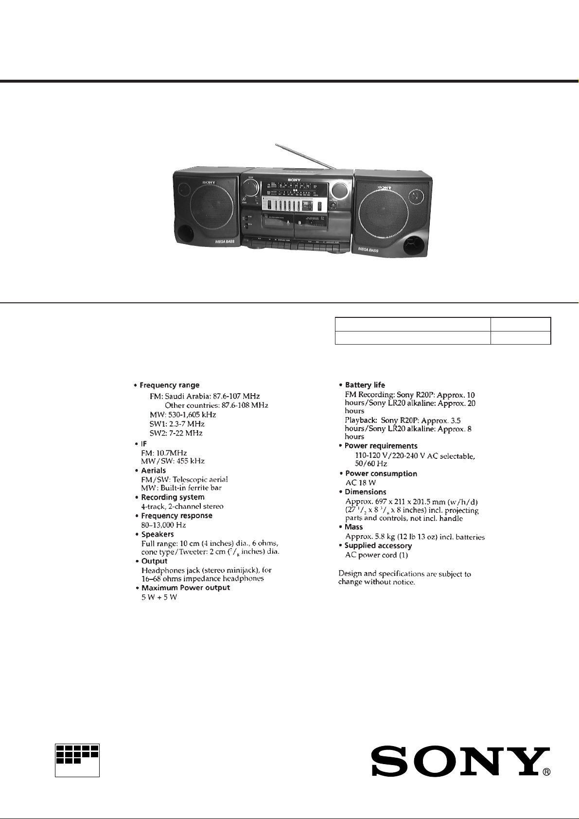
SPECIFICATIONS
E Model
Model Name Using Similar Mechanism NEW
Tape Transport Mechanism Type MF-W616-148
MICROFILM
RADIO CASSETTE-CORDER
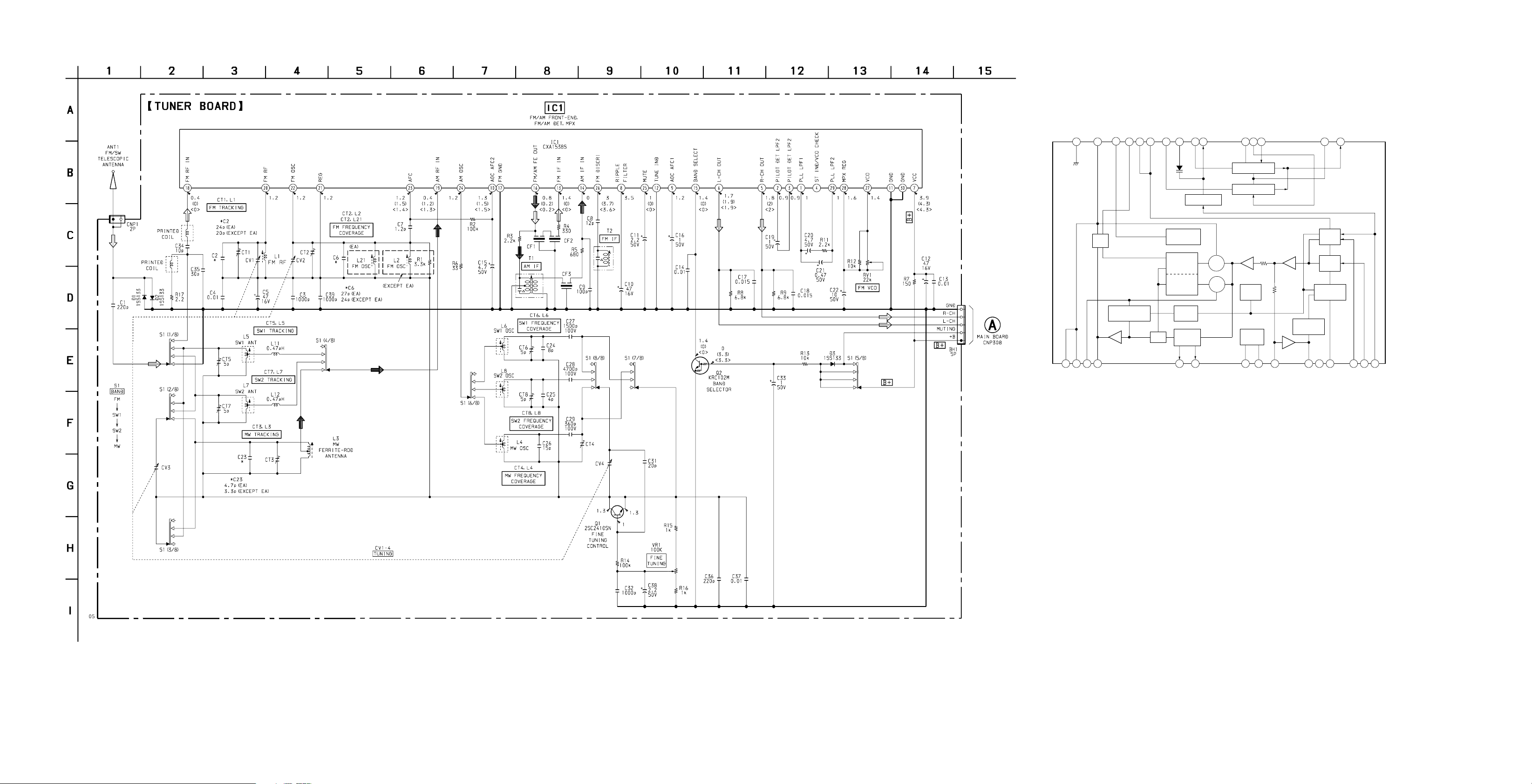
6-4. SCHEMATIC DIAGRAM – TUNER Section –
• IC Block Diagram
IC1 CXA1238S
GND
PLL LPF2
MPX REG
28
2930 242526 212223 181920 1617
27
VCO
MUTE
FM DISCRI
AM OSC
AFC
REGULATOR
REG
FM OSC
FM RF IN
AM RF IN
FM RF
FM FRONT-END
AM FRONT-END
FM GND
CFS-616S
FM/AM FE OUT
MPX
VCO
MONO/STEREO
SELECT
1
2 3 4 5 6 7 8 9
PLL LPF1
PILOT DET LPF2
PILOT DET LPF2
ST IND/VCO CHECK
REGULATOR
1/2
COUNTER
1/2
COUNTER
MUTING
DECORD
AMP
R-CH OUT
L-CH OUT
PD1
PD2
AUTO
BLEND
RIPPLE
FILTER
VCC
AGC AFC1
RIPPLE FILTER
BAND-PASS
MUTE
10
AGC AFC2
FM IF/
DISCRI
AM IF/
DET
TUNING
INDICATOR
11
12
GND
TUNE IND
13
FM IF IN
14
AM IF IN
15
BAND SELECT
Note on Schematic Diagram:
• All capacitors are in µF unless otherwise noted. pF: µµF
50 WV or less are not indicated except for electrolytics
and tantalums.
• All resistors are in Ω and 1/4 W or less unless otherwise
specified.
¢
•
: internal component.
• C : panel designation.
• U : B+ Line.
• H : adjustment for repair.
• Power voltage is dc 9V and fed with regulated dc power
supply from battery terminal.
• Voltages are dc with respect to ground under no-signal
(detuned) conditions.
no mark : FM
( ) : MW
< > : SW
• V oltages are taken with a V OM (Input impedance 10 MΩ).
Voltage variations may be noted due to normal production tolerances.
• Signal path.
F: FM/SW
f: MW
• Abbreviation
EA: Saudi Arabia model.
– 21 – – 22 – – 23 –
 Loading...