Sony CFDS-40-CP Service manual
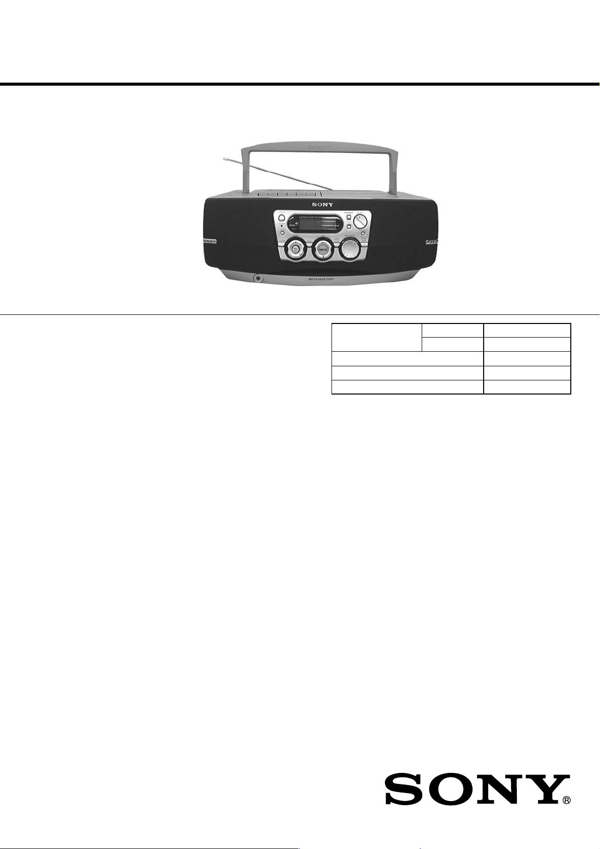
CFD-S40CP
SERVICE MANUAL
Ver. 1.3 2005.09
US Model
Canadian Model
AEP Model
UK Model
E Model
Model Name Using CD Section CFD-V3/V7/V7L
Similar Mechanism Tape Section CFD-V3/V5/V7/V7L
CD Mechanism Type KSM-213CDM
Optical Pick-up Type KSS-213C
Tape Transport Mechanism Type MF-V5-117
AUDIO POWER SPECIFICATIONS (US Model)
POWER OUTPUT AND TOTAL HARMONIC
DISTORTION
With 3.2-ohm loads, both channels driven from
150 - 10,000 Hz; rated 1.8 W per channel-minimum
RMS power, with no more than 10 %
total harmonic distortion in AC operation.
Other Specifications
CD player section
System
Compact disc digital audio system
Laser diode properties
Material: GaAlAs
Wave length: 780 nm
Emission duration: Continuous
Laser output: Less than 44.6 µW
(This output is the value measured at a distance of about
200 mm from the objective lens surface on the optical
pick-up block with 7 mm aperture.)
Spindle speed
200 r/min (rpm) to 500 r/min (rpm) (CLV)
Number of channels
2
Frequency response
20 - 20 000 Hz +1/–2 dB
Wow and flutter
Below measurable limit
SPECIFICATIONS
Radio section
Frequency range
FM: 87.5 - 108 MHz
AM: 530 - 1,710 kHz (US, CND, KR, TW)
MW: 531 - 1,611 kHz (AEP, UK)
LW: 153 - 279 kHz (AEP, UK)
Antennas
FM: Telescopic antenna
AM: Built-in ferrite bar antenna
Cassette-corder section
Recording system
4-track 2 channel stereo
Fast winding time
Approx. 120 sec. with Sony cassette C-60
Frequency response
TYPE I (normal): 70 - 13 000 Hz
General
Speaker
Full range: 10 cm (4 in.) dia.,
3.2 Ω, cone type (2)
Outputs
Headphones jack (stereo minijack)
For 16 - 68 Ω impedance headphones
Power output
2.3 W + 2.3 W (at 3.2 Ω, 10 % harmonic
distortion)
– Continued on page 2 –
9-873-092-14
2005I02-1
© 2005.09
CD RADIO CASSETTE-CORDER
Sony Corporation
Personal Audio Group
Pubulished by Sony Engineering Corporation
CFD-S40CP
Ver 1.1 2001.07
Power requirements
For CD radio cassette-corder:
120 V AC, 60 Hz (US, CND, TW)
230 V AC, 50 Hz (AEP, UK, KR)
9 V DC, 6 size D (R20) batteries
For memory back-up:
6 V DC, 4 size AA (R6) batteries
For remote control:
3 V DC, 2 size AA (R6) batteries
Power consumption
AC 20 W
Battery life
For CD radio cassette-corder:
FM recording
Sony R20P: approx. 15 h
Sony alkaline LR20: approx. 40 h
Tape playback
Sony R20P: approx. 10 h
Sony alkaline LR20: approx. 25 h
CD playback
Sony R20P: approx. 1.5 h
Sony alkaline LR20: approx. 6 h
Dimensions
Approx. 420 × 161 × 266 mm (w/h/d)
(16 5 ⁄8 × 6 3 ⁄8 × 10 1 ⁄2 inches) (incl. projecting parts)
Mass
Approx. 4.6 kg (10 lb. 2 oz) (incl. batteries)
Supplied accessories
AC power cord (1)
Remote control (1)
Design and specifications are subject to change without
notice.
Information
For customers in Europe
This Compact Disc player is classified as a CLASS 1 LASER
product.
The CLASS 1 LASER PRODUCT label is located at the bottom
of the player.
CAUTION
Use of controls or adjustments or performance
of procedures other than those specified herein
may result in hazardous radiation exposure.
SAFETY-RELATED COMPONENT WARNING!!
COMPONENTS IDENTIFIED BY MARK 0 OR DOTTED LINE WITH
MARK 0 ON THE SCHEMATIC DIAGRAMS AND IN THE PARTS
LIST ARE CRITICAL TO SAFE OPERATION.
REPLACE THESE COMPONENTS WITH SONY PARTS WHOSE
PART NUMBERS APPEAR AS SHOWN IN THIS MANUAL OR IN
SUPPLEMENTS PUBLISHED BY SONY.
ATTENTION AU COMPOSANT AYANT RAPPORT
À LA SÉCURITÉ!!
TABLE OF CONTENTS
Specifications ............................................................................... 1
1. SERVICING NOTES ...................................................... 3
2. GENERAL
Location and Function of Controls ....................................... 4
3. DISASSEMBLY
3-1. Cabinet (Front) ASSY, Cabinet (Rear) ........................ 7
3-2. Control Board .............................................................. 8
3-3. Headphone Board ........................................................ 8
3-4. Cabinet (Upper) ASSY ................................................ 9
3-5. LCD Board (with Lamp Board) ................................... 9
3-6. Main Board ................................................................ 10
3-7. CD Board ................................................................... 10
3-8. Optical Pick-up Block, Mechanism Deck,
CD motor Board, TC Board ....................................... 11
3-9. M321 (Capstan/Reel Motor), Belt,
HRP301 Head, Magnetic (Record/Playback),
HE301 Head (Erase) .................................................. 11
3-10. Power ASSY, Battery Board,
Battery Common Board ............................................. 12
3-11. Tuner Board ............................................................... 12
4. ADJUSTMENTS
4-1. Mechanical Adjustments ........................................... 13
4-2. Electrical Adjustments ............................................... 13
5. DIAGRAMS
5-1. Explanation of IC Terminals ...................................... 17
5-2. Block Diagram – Tuner/TC Section – ....................... 20
5-3. Block Diagram – Main Section – .............................. 21
5-4. Block Diagram – CD Section – ................................. 22
5-5. Printed Wiring Board – TC Section – ........................ 23
5-6. Schematic Diagram – TC Section – .......................... 23
5-7. Printed Wiring Board
– Tuner Section (US, Canadian, KR, TW Model) – .. 24
5-8. Schematic Diagram
– Tuner Section (US, Canadian, KR, TW Model) – .. 25
5-9. Printed Wiring Board
– Tuner Section (AEP, UK Model) –......................... 26
5-10. Schematic Diagram
– Tuner Section (AEP, UK Model) –......................... 27
5-11. Printed Wiring Board – CD Section – ....................... 28
5-12. Schematic Diagram – CD Section (1/2) – ................. 29
5-13. Schematic Diagram – CD Section (2/2) – ................. 30
5-14. Schematic Diagram – Main Section (1/2) – .............. 31
5-15. Schematic Diagram – Main Section (2/2) – .............. 32
5-16. Printed Wiring Board – Main Section – .................... 33
5-17. Printed Wiring Board – Power Supply Section – ...... 34
5-18. Schematic Diagram – Power Supply Section – ......... 34
6. EXPLODED VIEWS
6-1. Front Cabinet Section ................................................ 40
6-2. Rear Cabinet Section ................................................. 41
6-3. Upper Cabinet Section ............................................... 42
6-4. Mechanism Deck Section (1) .................................... 43
6-5. Mechanism Deck Section (2) .................................... 44
6-6. CD Block Section ...................................................... 45
LES COMPOSANTS IDENTIFIÉS PAR UNE MARQUE 0 SUR
LES DIAGRAMMES SCHÉMATIQUES ET LA LISTE DES
PIÈCES SONT CRITIQUES POUR LA SÉCURITÉ DE
FONCTIONNEMENT. NE REMPLACER CES COMPOSANTS
QUE PAR DES PIÈCES SONY DONT LES NUMÉROS SONT
DONNÉS DANS CE MANUEL OU DANS LES SUPPLÉMENTS
PUBLIÉS PAR SONY.
2
7. ELECTRICAL PARTS LIST...................................... 46
SECTION 1
SERVICING NOTES
CFD-S40CP
SAFETY CHECK-OUT (US model)
After correcting the original service problem, perform the
following safety check before releasing the set to the customer:
Check the antenna terminals, metal trim, “metallized” knobs,
screws, and all other exposed metal parts for AC leakage. Check
leakage as described below.
LEAKAGE TEST
The AC leakage from any exposed metal part to earth ground and
from all exposed metal parts to any exposed metal part having a
return to chassis, must not exceed 0.5 mA (500 microamperes).
Leakage current can be measured by any one of three methods.
1. A commercial leakage tester, such as the Simpson 229 or RCA
WT-540A. Follow the manufacturers’ instructions to use these
instruments.
2. A battery-operated AC milliammeter. The Data Precision 245
digital multimeter is suitable for this job.
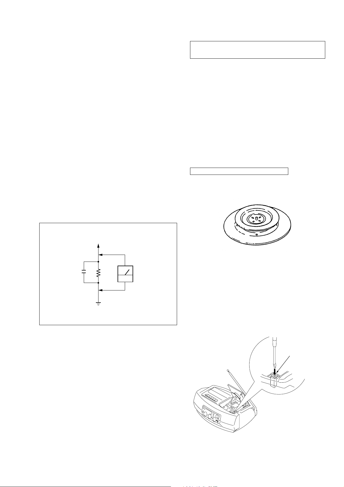
3. Measuring the voltage drop across a resistor by means of a VOM
or battery-operated AC voltmeter. The “limit” indication is 0.75
V, so analog meters must have an accurate low-voltage scale.
The Simpson 250 and Sanwa SH-63Trd are examples of a passive VOM that is suitable. Nearly all battery operated digital
multimeters that have a 2V AC range are suitable. (See Fig. A)
NOTES ON HANDLING THE OPTICAL PICK-UP
BLOCK OR BASE UNIT
The laser diode in the optical pick-up block may suffer electrostatic breakdown because of the potential difference generated
by the charged electrostatic load, etc. on clothing and the human
body.
During repair, pay attention to electrostatic breakdown and also
use the procedure in the printed matter which is included in the
repair parts.
The flexible board is easily damaged and should be handled
with care.
NOTES ON LASER DIODE EMISSION CHECK
The laser beam on this model is concentrated so as to be focused
on the disc reflective surface by the objective lens in the optical
pick-up block. Therefore, when checking the laser diode
emission, observe more than 30 cm away from the objective
lens.
CHUCK PLATE JIG ON REPAIRING
On repairing CD section, playing a disc without the CD lid, use
Chuck Plate Jig.
• Code number of Chuck Plate Jig : X-4918-255-1
To Exposed Metal
Parts on Set
0.15
µ
F
Ω
1.5k
Earth Ground
AC
voltmeter
(0.75V)
Fig. A. Using an AC voltmeter to check AC leakage.
LASER DIODE AND FOCUS SEARCH OPERATION
CHECK
1. Press CD open knob.
2. Open the lid for CD.
3. Push on SWITCH (S701) as following figure.
4. Confirm the laser diode emission while observing the
objecting lens. When there is no emission, Auto Power
Control circuit or Optical Pick-up is broken.
Objective lens moves up and down once for the focus
search.
Insert a precision
screw driver and push
SWITCH (S701)
3
CFD-S40CP
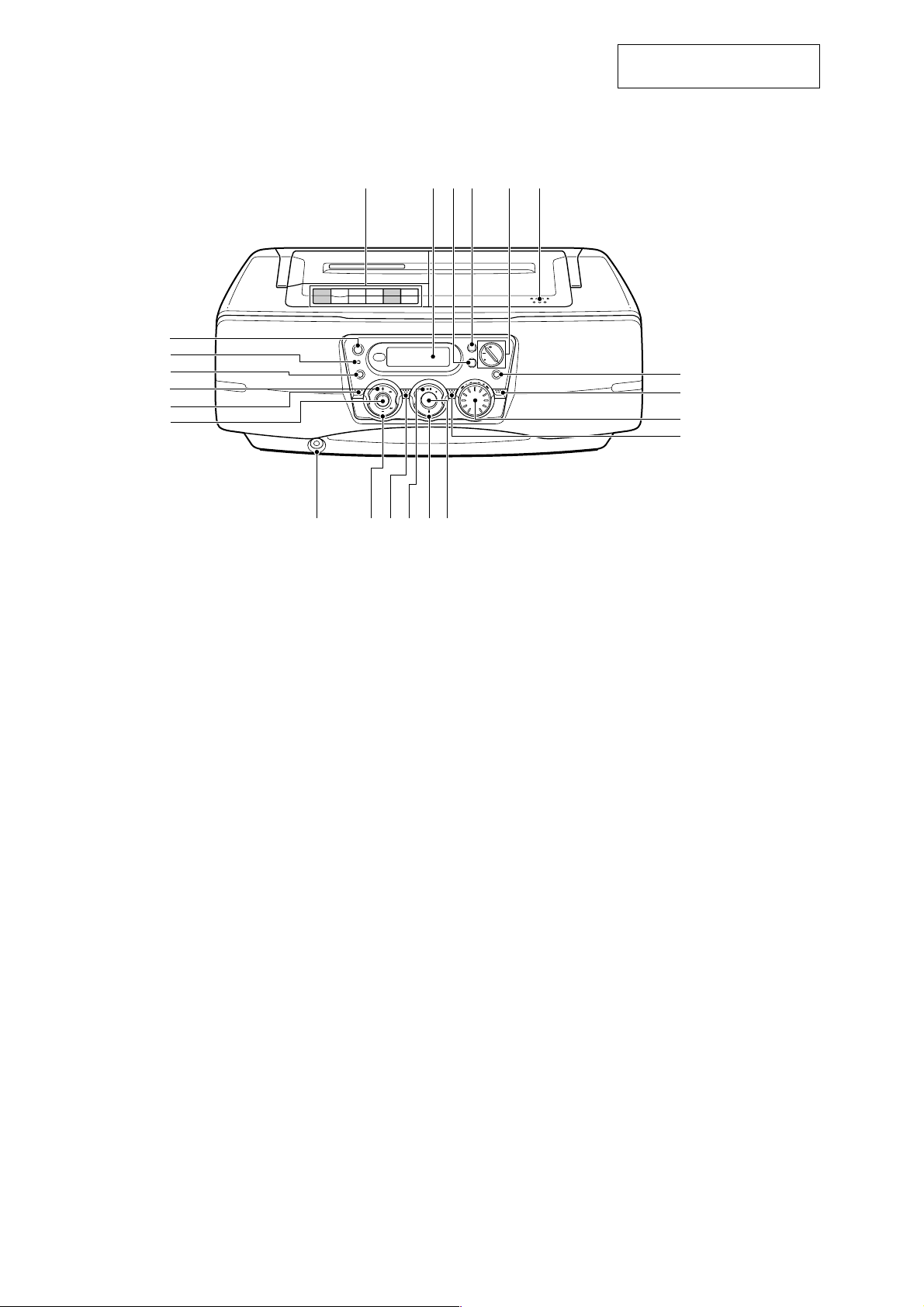
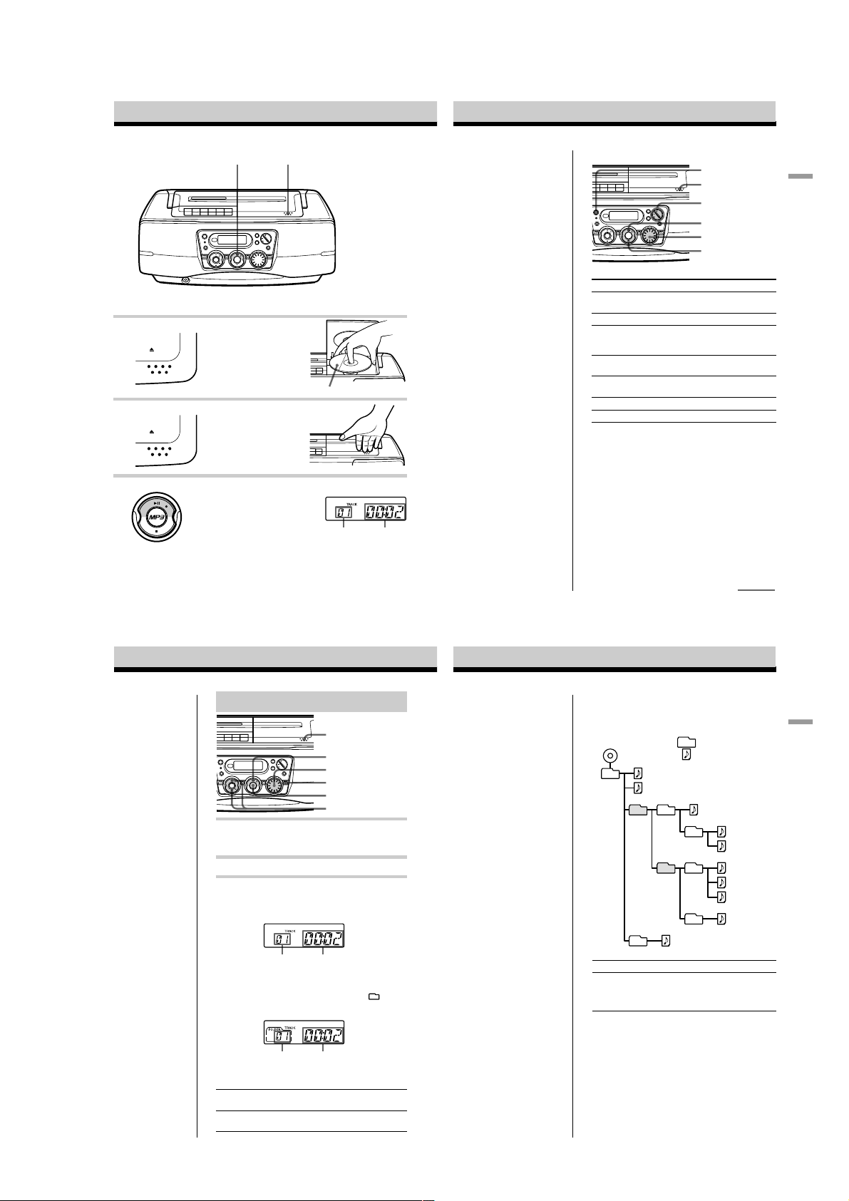
LOCATION AND FUNCTION OF CONTROLS
6
5
4
3
2
1
SECTION 2
GENERAL
7 8 9 0 qa qs
This section is extracted from
instruction manual.
qd
qf
qg
qh
1 BAND•AUTO PRESET button
2 FUNCTION button
3 CD: M
Radio: TUNE + button
4 SLEEP
5 OPR/BATT indicator
6 POWER button
7 Tape operation buttons
REC z
PLAY N
REW m
FF M
STOP/EJECT x/Z
PAUSE X
8 Display window
9 SOUND button
qkqlw;waws qj
0 MEGA BASS button
qa VOLUME +/- button
qs Z PUSH OPEN/CLOSE
qd DISPLAY/ENTER•MEMORY button
qf FOLDER/TRACK button
qg AMS/PRESET +/- Jog dial
qh INTRO SCAN button
qj MP3 indicator
qk CD x button
ql CD u button
w; MODE button
wa CD: m
Radio: TUNE - button
ws i jack
4
Basic Operations
CFD-S40CP
Playing an audio CD or MP3 files
3
1, 2
Connect the supplied AC power cord (see page 23).
1 Press Z PUSH OPEN/CLOSE down
PUSH
OPEN/CLOSE
to open the CD compartment and
place the CD on the CD
compartment.
2 Close the lid of the CD compartment.
PUSH
OPEN/CLOSE
3 Press u (N on the remote).
CD
The player turns on (direct power-on)
and the player plays all the tracks
once.
To play a disc with MP3 files, see
page 6.
With the label side up
Display
Tra ck
number
Playing
time
Tip
Playback starts from the
track you last stopped
playing (Resume play).
During stop, the track
number to be played are
displayed.
To cancel the resume play
to start play from the
beginning of the first track,
press x in stop mode.
Use these buttons for additional operations
POWER
Z
PUSH
OPEN/CLOSE
VOLUME +, –
u
Jog dial
x
To Do this
adjust the volume Press VOLUME +, —
stop playback Press x .
pause playback Press u (X on the remote).
go to the next track Turn the jog dial clockwise.
go back to the previous track Turn the jog dial counterclockwise.
remove the CD* Press Z PUSH OPEN/CLOSE.
turn on/off the player Press POWER.
*Once you open the CD compartment, the track to start play will
change to the beginning of the first track.
(VOL +, — on the remote).
Press the button again to
resume play after pause.
(On the remote, press >.)
(On the remote, press ..)
Basic Operations
4
Playing an audio CD or MP3 files (continued)
Playing a disc with MP3 files
Note
Before playing a file, this
player reads all file and
folder information on the
disc. Depending on the
file structure, it may take
more than a minute to
read them. During this
time, TOC READING
is displayed.
Tip
You can use the buttons
mentioned on page 5 for
additional operations in
the same way as playing
an audio CD.
1
Press Z PUSH OPEN/CLOSE down to open the CD
compartment and place the CD on the CD compartment
(see page 4) .
2
Close the lid of the CD compartment.
3
Press u (N on the remote).
The player turns on and the player plays all files of a disc
(TRACK mode).
When you use a disc with MP3 files, the MP3 indicator
lights up.
Track number
Playing a specific file (FOLDER mode)
Press FOLDER/TRACK during stop to display
display, and turn the jog dial to select the folder you want to
play, then press
After the file name is displayed,
the playing time will appear
u.
Z PUSH
OPEN/CLOSE
u
Jog dial
FOLDER/TRACK
MP3 indicator
M, m
continued
5
Example of folder structure and playing
order
The playing order of the folders and files is as follows:
CD-R
CD-RW
1
1
Folder
MP3 file
Basic Operations
2
Notes
¥ A folder that does not
include an MP3 file is
skipped.
¥ Maximum folder number:
255
Maximum file number: 255
¥ Folder names and file
names can be displayed
with up to 8 characters.
¥ The characters A - Z,
0 - 9, and _ can be
displayed on this player.
Other characters are
displayed as - .
¥ The file name does not
correspond to the ID tag.
Track mode Playing all MP3 files from 1, 2, 3...9, 0
Folder mode Playing all MP3 files in the selected folder.
in
the
3
4
4
5
6
5
7
8
9
6
q;
2
3
(Example: If you select folder 3, the player
plays file 4. If you select folder 4, the player
plays file 5 and 6.)
Folder number
To go to the next track / go back to the previous
track in the selected folder
During play Turn the jog dial.
During stop Press M or m.
6
After the folder name is displayed,
the playing time will appear
(Press > or . on the remote)
(Press TUNE + or - on the remote)
7
5

CFD-S40CP
About “MP3”
What is the MP3?
MP3 (MPEG 1 Audio Layer-3) is a standard
technology and format for compressing a
sound sequence. The file is compressed to
about 1/10 of its original size. Sounds
outside the range of human hearing are
compressed while the sounds we can hear
are not compressed.
Playable “MP3” files on this
player
You can only play MP3 files recorded by
following requirements.
USABLE MEDIA
CD-Rs and CD-RWs
USABLE DISC FORMAT
You can use ISO 9660 Level 1 format discs,
not including the expanded format. In
some cases, MP3 files that are recorded in a
format other than ISO 9660 Level 1 may not
play normally or the file and folder names
may not be displayed correctly.
The major specifications of the ISO 9660
Level 1 format are as follows:
¥ Maximum directory steps: 8
¥ Usable characters for a file/folder name:
A - Z, 0 - 9, _ (underscore)
¥ Maximum number of characters for a file
name: 12 including quotation marks and a
3-character extension code
Notes
¥ The file names and folder names must be ISO
9660 level 1 compliant.
¥ When naming, be sure to add the file extension
mp3 to the file name.
¥ If you put the extension mp3 to a file other
than MP3, the player cannot recognize the file
properly and will generate random noise that
could damage your speakers.
¥ The file name does not correspond to the ID tag.
THE USABLE NUMBER OF
FOLDERS/FILES
¥ Maximum folder number: 255
¥ Maximum file number: 255
SETTINGS FOR COMPRESSION
SOFTWARE AND WRITING
SOFTWARE
¥ To compress a source for an MP3 file, we
recommend setting the transfer bit rate of
the compression software to 44.1 kHz ,
128kbps , and Constant Bit Rate .
¥ To record up to the maximum capacity, set
to the halting of writing .
¥ To record at one time up to the maximum
capacity on media that has nothing
recorded it, set to Disc at Once .
NOTES FOR SAVING FILES ON
THE MEDIA
When the disc is inserted, the player reads
all the files on that disc. If there are many
folders or non-MP3 files on the disc, it may
take a long time for play to begin or for the
next MP3 file to start play.
Do not save unnecessary folders or files
other than MP3 ones in the disc to be used
for MP3 listening.
We recommend that you do not save other
types files or unnecessary folders on a disc
that has MP3 files.
30
6
DISASSEMBLY
)
z
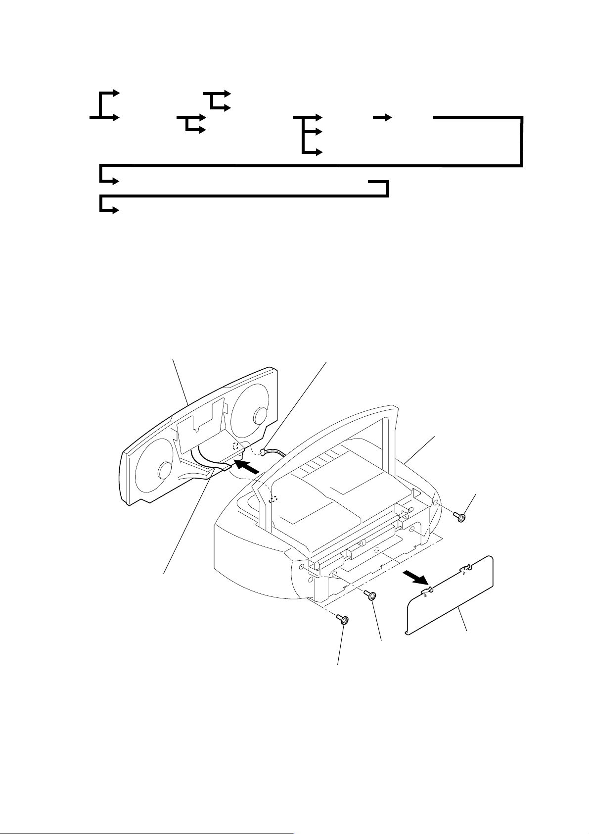
The equipment can be removed using the following procedure.
CFD-S40CP
SECTION 3
Cabinet (front) ASSY
Control board
Headphone board
Set
Cabinet (rear) Cabinet (upper) ASSY
Tuner board
Optical pick-up block, Mechanism deck, CD motor board, TC board
M321 (Capstan/reel motor), Belt, HRP301 Head magnetic (Record/play back), HE301 Head (Erase)
Note : Follow the disassembly procedure in the numerical order given.
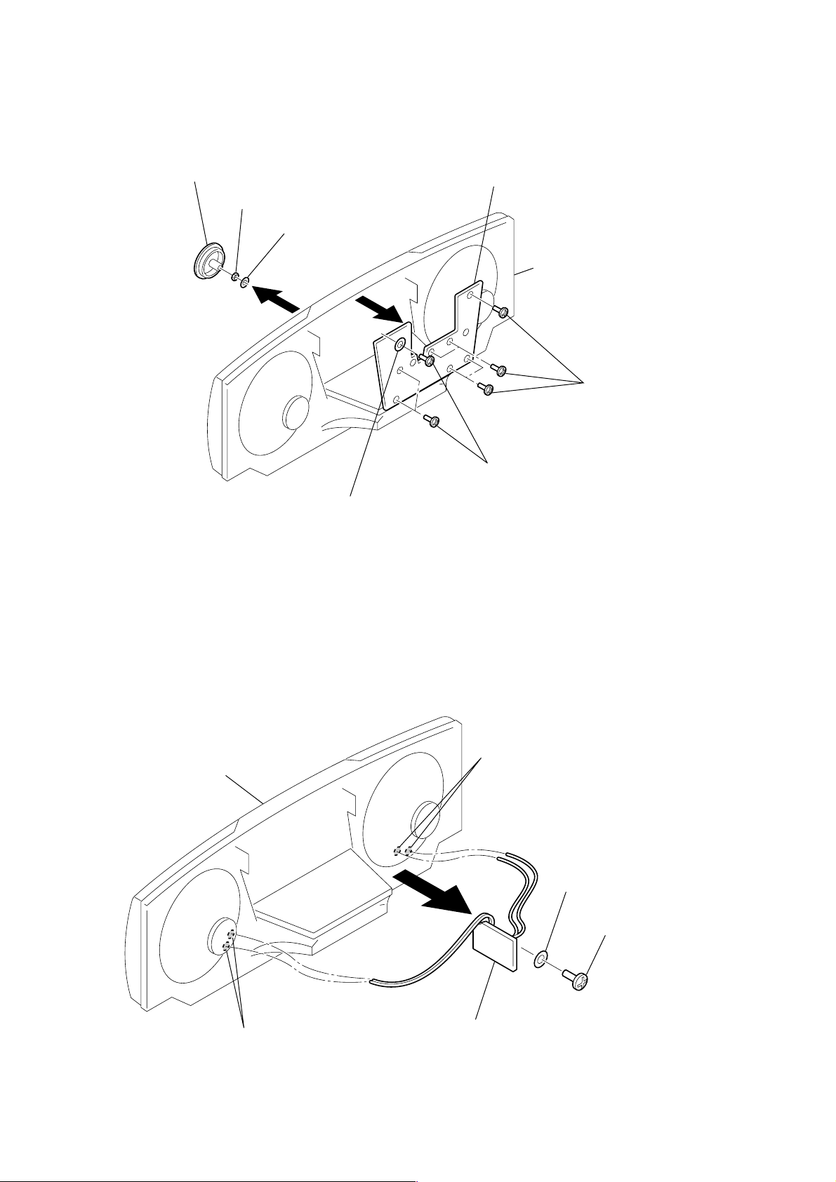
3-1. CABINET (FRONT) ASSY, CABINET (REAR)
7 Cabinet (front) ASSY
Main board CD board
LCD board (with lamp board)
Power ASSY, Battery board, Battery common board
6 Connector
(from Headphone board CNP306)
5 Cable, flexible flat
(from Main board CNP801)
4
2 Screws
(+BVTP 3 × 14)
3 Screws
(+BVTP 3 × 14)
Cabinet (rear)
2 Screws
(+BVTP 3 × 14
1
Lid, battery case
7
CFD-S40CP
)
)
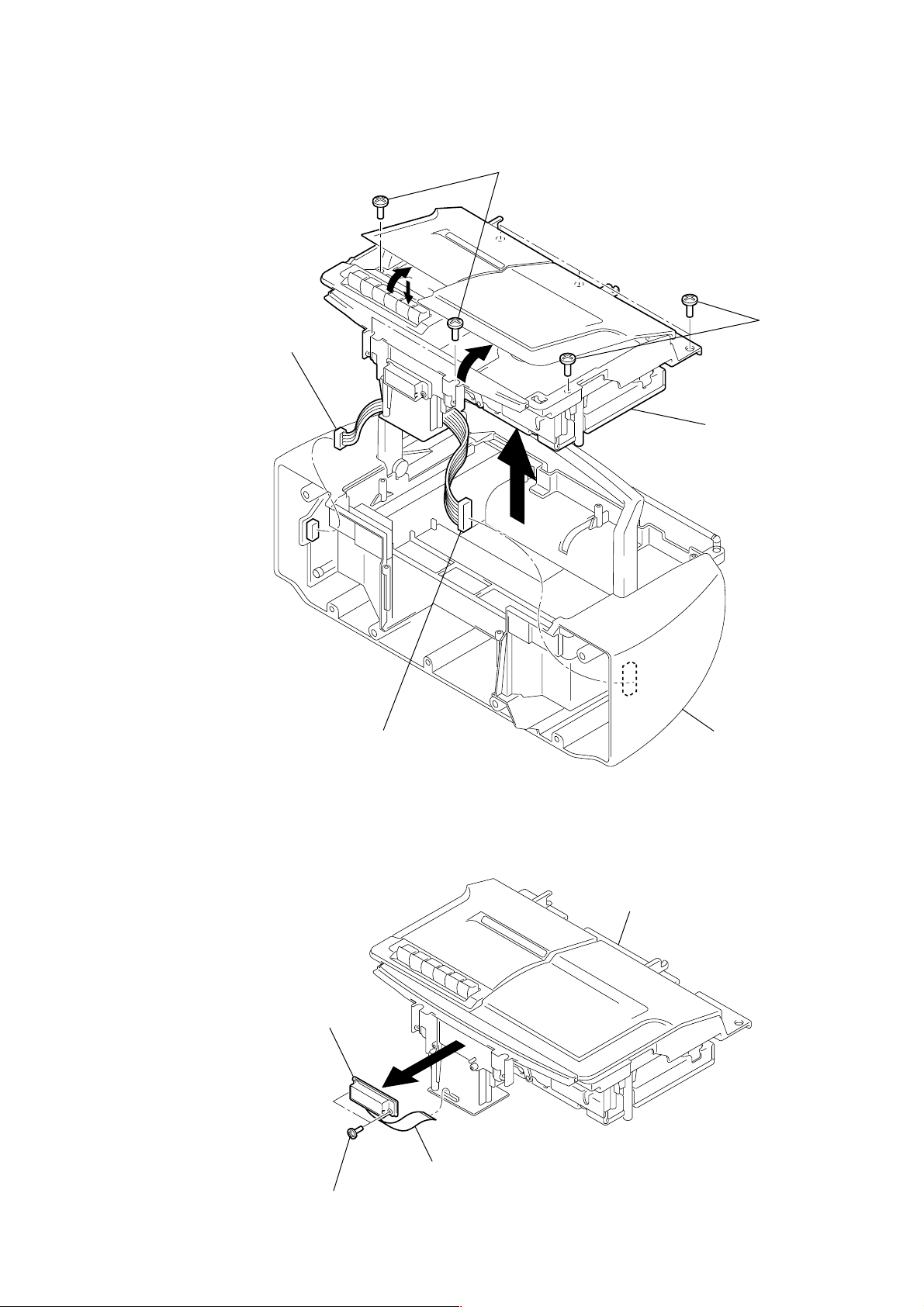
3-2. CONTROL BOARD
1 Dial, jog
6 Control board
2 Hexagonal nut
3 Washer
Cabinet (front) ASSY
4 Screws
(+BVTP 2.6 × 10
4 Screws
(+BVTP 2.6 × 10)
5 PWB, retainer
3-3. HEADPHONE BOARD
Cabinet (front) ASSY
2 Remove solder
(two places)
1 Remove solder (two places)
4 PWB, retainer
3 Screw
(+BVTP 2.6 x 10
5 Headphone board
8
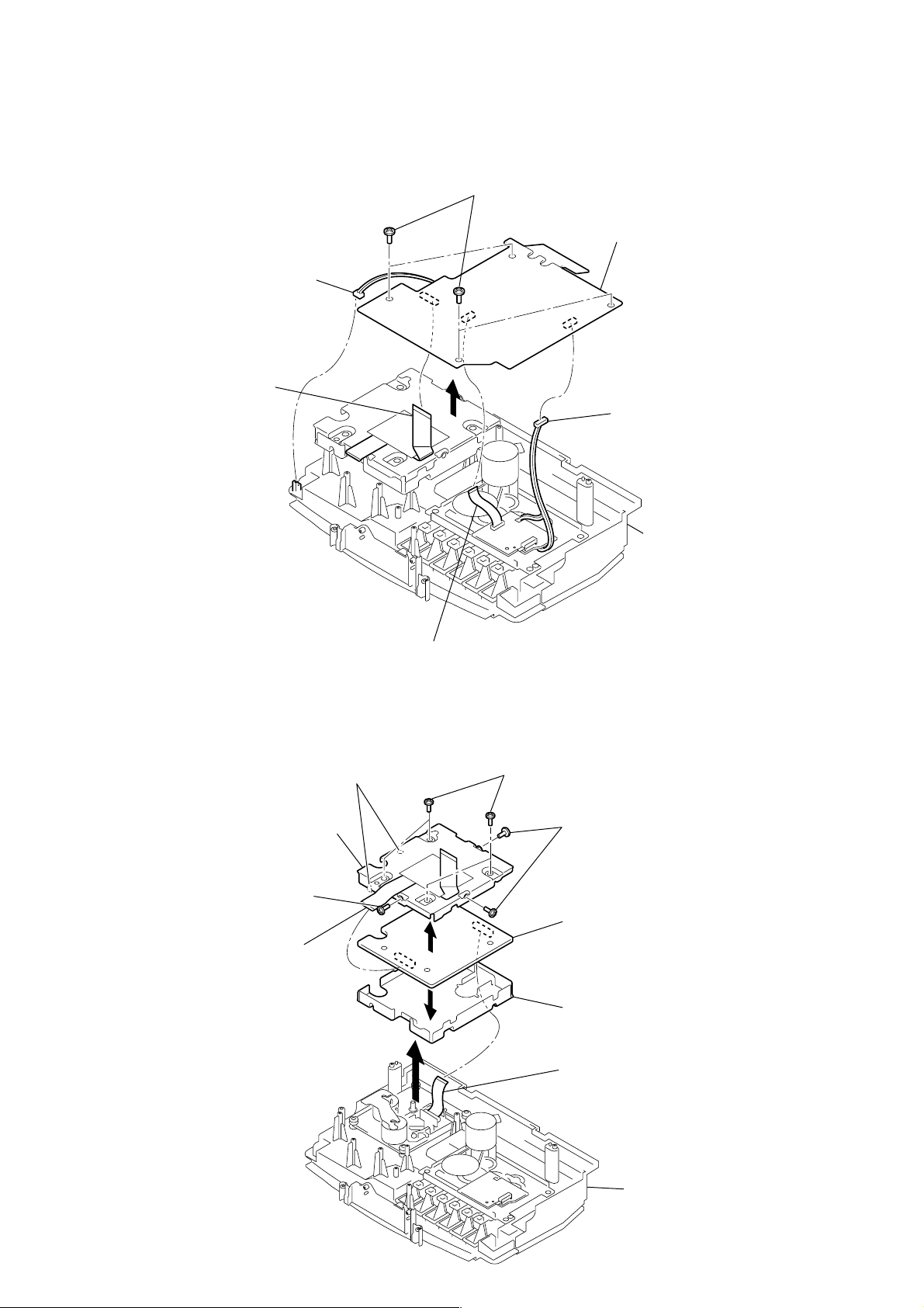
3-4. CABINET (UPPER) ASSY
CFD-S40CP
5 Screws
(+BVTP 3 × 10)
4
3
1 Connector
(from Tuner board CNP902)
2
1 Connector
(from Tuner board CNP1)
5 Screws
(+BVTP 3 × 10)
Cabinet (upper) ASSY
6
Cabinet (rear)
3-5. LCD BOARD (WITH LAMP BOARD)
LCD board
(with Lamp board)
1 Screws
(+BVTP 3 × 12)
Cabinet (upper)
2
3 Cable, flexible flat (34 core)
(from Main board CNP851)
9
CFD-S40CP
)
)
3-6. MAIN BOARD
5
Cable, flexible flat
(from Main board CNP802)
1
Connector
(from S701)
2
Screws (+BVTP 3 × 10)
3
Main board
6
Connector
(from Main board CNP322
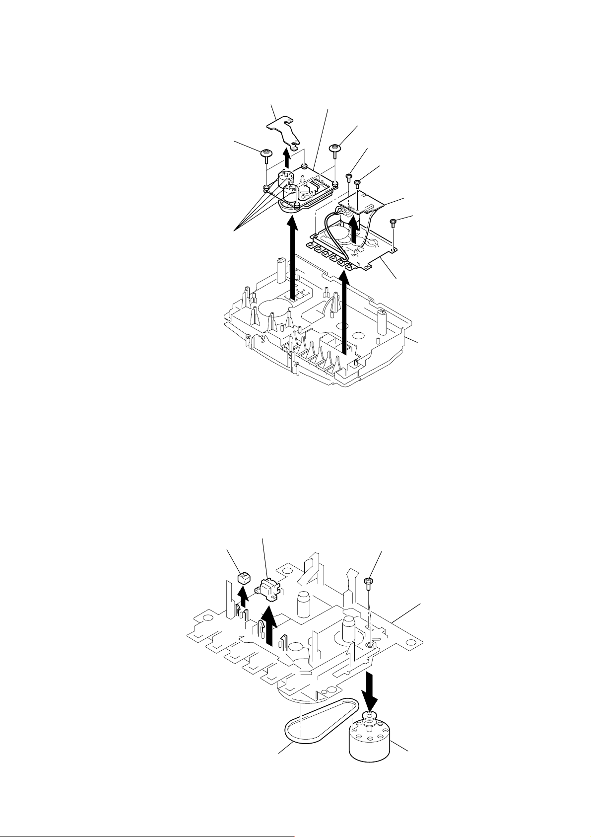
3-7. CD BOARD
5 Remove solder
(2 places)
7 Plate (lower), shield
6 Screw
(+BVTT 2 × 4)
4 Cable, flexible flat
(from CD board CN1001)
Cabinet (upper)
4
Cable, flexible flat (US, CND: 9 core, AEP, UK: 11 core)
(from Main board CNP805)
1 Screws (+BVTP 3 × 10)
6 Screws
(+BVTT 2 × 4)
9 CD board
10
2
8 Plate (upper), shield
3 Cable, flexible flat (16 core
(from CD board CN1003)
Cabinet (upper)
)
)
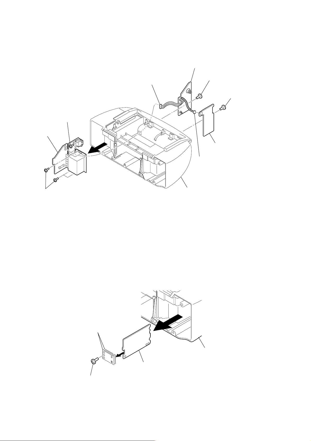
3-8. OPTICAL PICK-UP BLOCK, MECHANISM DECK, CD MOTOR BOARD, TC BOARD
CFD-S40CP
1 Screws
(+PWH 2.6 × 10)
3 Remove solder
4 CD motor board
2 Optical pick-up block
1 Screws (+PWH 2.6 × 10)
5 Screws (+BVTP 3 × 10)
7 Screw (+BVTT 2 × 4)
8 TC board
5 Screw
(+BVTP 3 × 10
6 Mechanism deck
Cabinet (upper)
3-9. M321 (CAPSTAN/REEL MOTOR), BELT,
HRP301 HEAD, MAGNETIC (RECORD/PLAYBACK),
HE301 HEAD (ERASE)
5HRP301
6HE301
Head (erase)
Head, magnetic (record / playback)
1 Screws
+B 2.6 × 5
Mechanism deck
2
3 Belt
4 M321
(Capstan/reel motor
11
CFD-S40CP
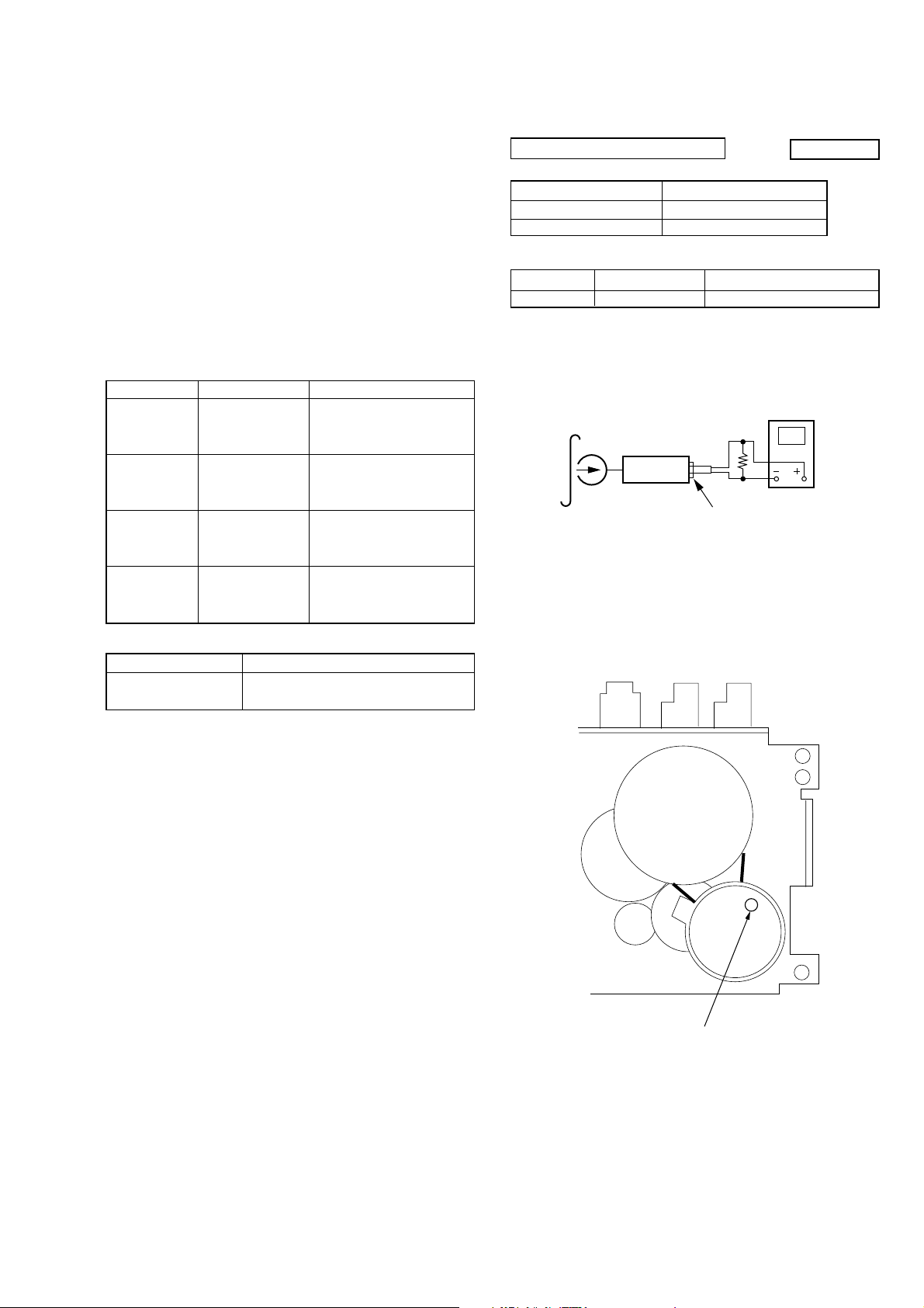
3-10. POWER ASSY, BATTERY BOARD, BATTERY COMMON BOARD
6 Battery board
Power ASSY
2 Screws
(+BVTP 3 × 14)
2 Screws
(+BVTP 3 × 10)
3
1 Connector
(from Secondary board CNP901)
5 Screw
(+WH 3 × 8)
5 Screw
(+WH 3 × 8)
6 Battery common board
4 Connector
(from Battery common
board CNP904)
Cabinet (rear)
3-11. TUNER BOARD
2 Tuner retainer boards
1 Screw
(+BVTP 3 × 10)
3
Cabinet (rear)
Tuner board
12
SECTION 4
y
ADJUSTMENTS
CFD-S40CP
4-1. MECHANICAL ADJUSTMENTS
PRECAUTION
1. Clean the following parts with a denatured-alcohol-moistened
swab :
record/playback head pinch roller
erase head rubber belts
capstan
2. Demagnetize the record/playback head with a head demagnetizer. (Do not bring the head demagnetizer close to the erase
head.)
3. Do not use a magnetized screwdriver for the adjustments.
4. The adjustments should be performed with the rated power supply voltage (9V) unless otherwise noted.
Torque Measurement
Torque Torque Meter Meter Reading
1.77 – 5.88 mN•m
Forward CQ-102C (18 – 60 g•cm)
(0.25 – 0.83 oz•inch)
Forward
Back Tension
Fast Forward CQ-201B (45 – 95 g•cm)
Rewind CQ-201B (45 – 95 g•cm)
CQ-102C (1.0 – 5.0 g•cm)
0.1 – 0.49 mN•m
(0.014 – 0.069 oz•inch)
4.42 – 9.31 mN•m
(0.62 – 1.32 oz•inch)
4.42 – 9.31 mN•m
(0.62 – 1.32 oz•inch)
4-2. ELECTRICAL ADJUSTMENTS
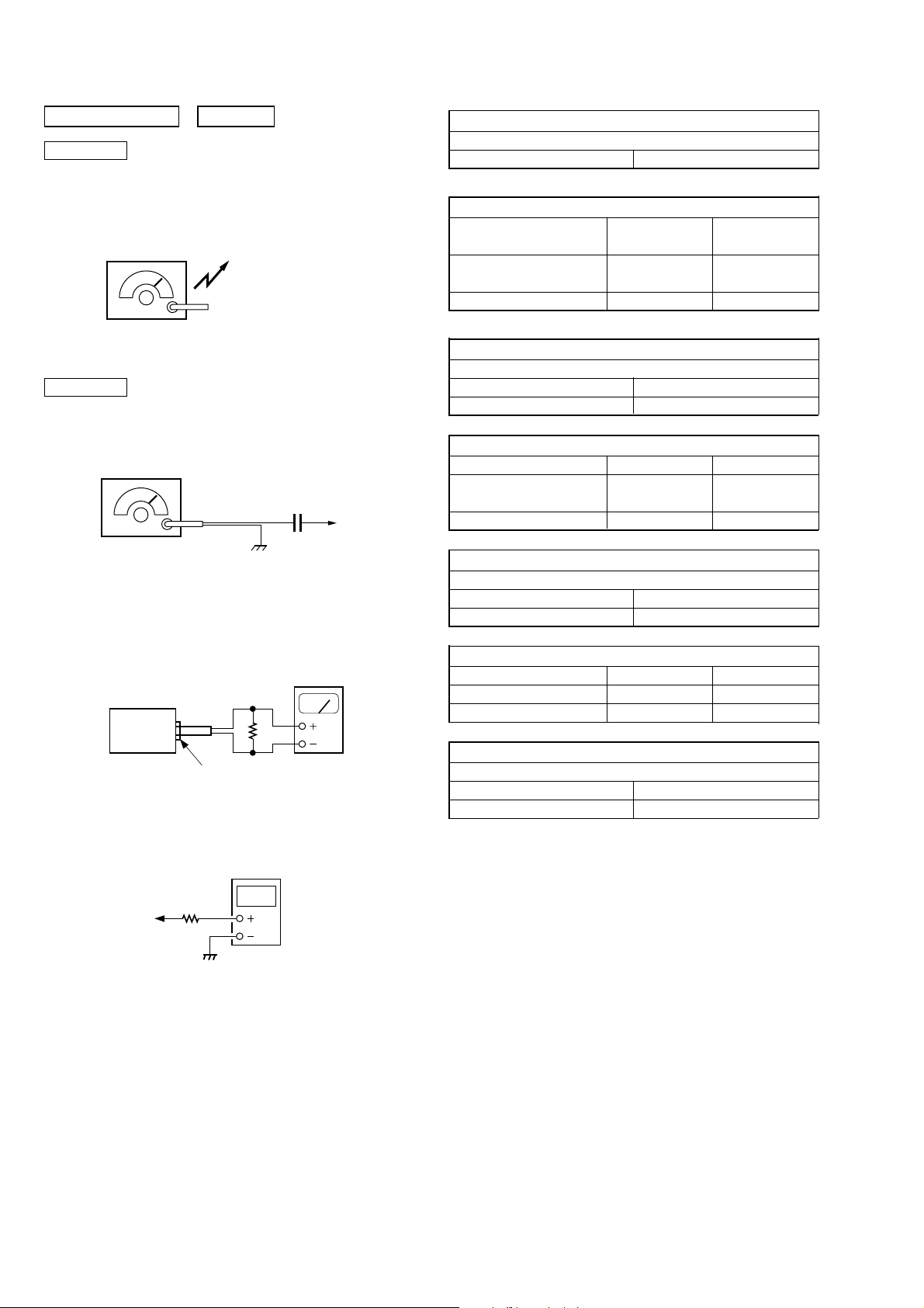
TAPE RECORDER SECTION
Standard Output Level
Output terminal HP OUT
load impedance 32 Ω
output signal level 0.25V (–10dB)
Test Tape
Type Signal Used for
WS-48A 3kHz, 0dB Tape Speed Adjustment
Tape Speed Adjustment
Procedure :
Mode : Playback
test tape
WS-48A
(3kHz, 0dB)
set
Adjustment Value : 3,000Hz
Standard Value : 2,940 - 3,060Hz
Frequency difference between the beginning and the end of the tape
should be within 1.5% (45Hz).
32Ω
J301 (phones)
0dB = 0.775V
digital frequenc
counter
Tape Tension Measurement
Torque Meter Meter Reading
CQ-403A
more than 60g
(more than 2.12 oz)
Adjustment Location : Mechanism deck
Tape speed adjustment
control inside motor
13
CFD-S40CP
c
)
Ver 1.1 12001.07
TUNER SECTION
0dB = 1 µV
AM Section
Function switch : AM (US, Canadian, Korean, Taiwan)
MW or LW (AEP, UK)
Volume : MIN
AM RF signal
generator
30% amplitude modulation by 400Hz
signal.
Output level : as low as possible
Put the lead-wire
antenna close to
the set.
FM Section
Function switch : FM
Volume : MIN
FM RF signal
generator
0.01µF
22.5kHz frequency deviation by
1kHz signal.
Output level : as low as possible
• Connecting Level Meter (FM and AM)
telescopi
antenna
terminal
MW/LW IF ADJUSTMENT
Adjust for a maximum reading on level meter.
T1 455kHz
( ): AEP, UK
AM (MW) FREQUENCY COVERAGE CHECK
Frequency Display
Reading on Digital voltmeter 1.0 (0.8)
Adjustment Part <confirmation> <confirmation>
AM (MW) TRACKING ADJUSTMENT
Adjust for a maximum reading on level meter.
L4 (L3) CT3
620 kHz (621 kHz) 1,400 kHz (1,404 kHz)
LW FREQUENCY COVERAGE ADJUSTMENT (AEP, UK)
Frequency Display 153 kHz 279 kHz
Reading on Digital voltmeter 0.7
Adjustment Part <confirmation> L4
LW TRACKING ADJUSTMENT (AEP, UK)
Adjust for a maximum reading on level meter.
L3 CT5
162 kHz 261 kHz
530 kHz 1,710 kHz
(531 kHz) (1,611 kHz)
+ 0.7 V
– 0.5 V – 0.6 V
+ 0.3 V
– 0.4 V
4.8 (5.0)
+ 1.2 V
( ): AEP, UK
5.0 ± 0.1 V
level meter
(range: 0.5–5 V ac
32 Ω
set
i jack
• Connecting Digital Voltmeter (FM and AM)
digital
voltmeter
100 kΩ
TP (VT)
(JW17)
• Repeat the procedures in each adjustment several times, and the
frequency coverage and tracking adjustments should be finally
done by the trimmer capacitors.
FM FREQUENCY COVERAGE ADJUSTMENT
Frequency Display 87.5 MHz 108 MHz
Reading on Digital voltmeter 1.6 ± 0.4 V 4.0 ± 0.3 V
Adjustment Part <confirmation> L2
FM TRACKING ADJUSTMENT
Adjust for a maximum reading on level meter.
L1 CT1
87.5 MHz 108 MHz
Adjustment Location : Main board (See page 15)
14
CFD-S40CP
)
)
2
C
7
Q1007
oscilloscope
(AC range)
TP 4002(FE)
IC 1007 10pin
CD BOARD (SIDE A)
2
1
B
0
CD SECTION
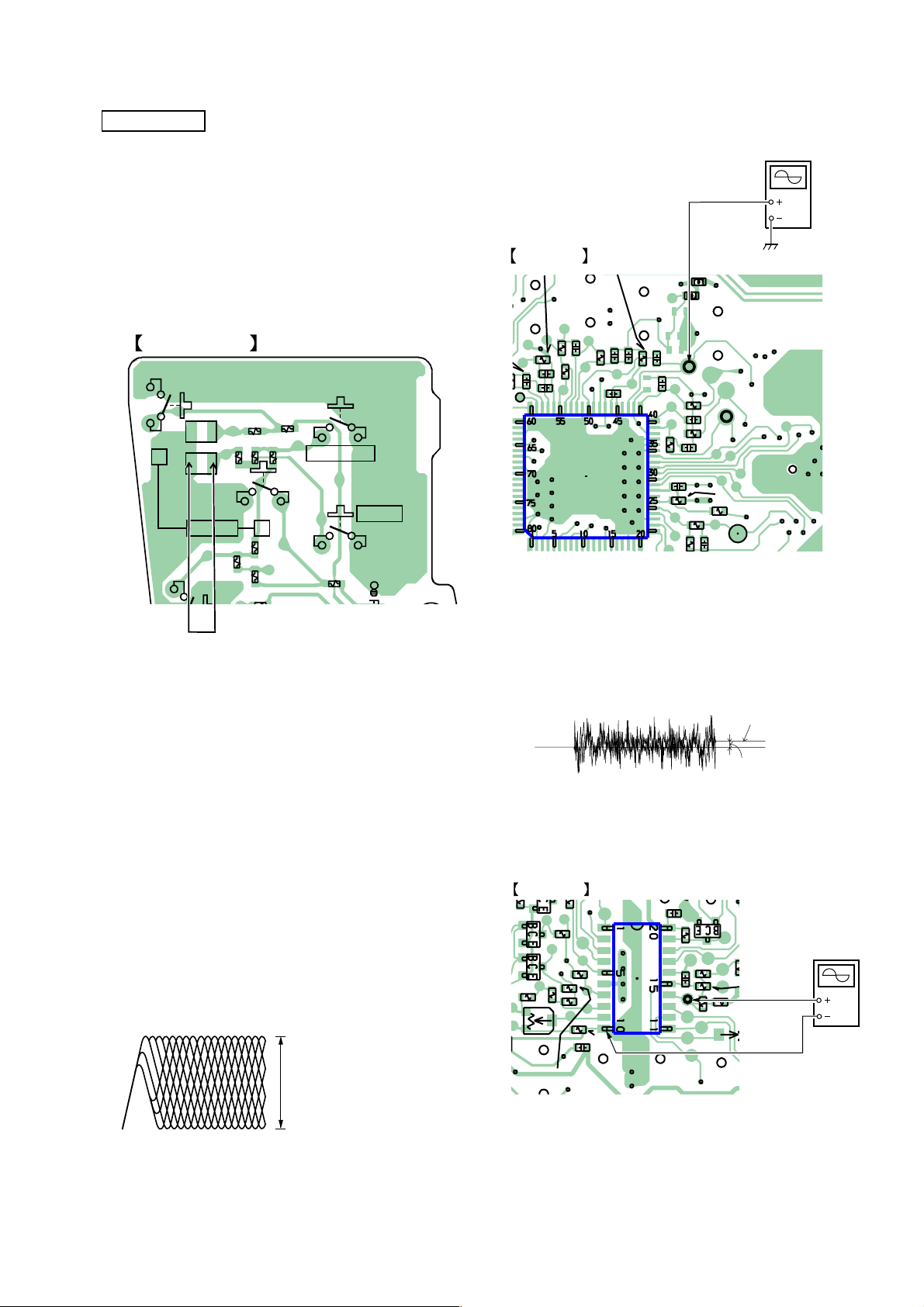
Perform all CD section check and all adjustments in the test mode.
How to put the set into CD test mode
1. Press the POWER button turn the set ON.
2. Press the FUNCTION button to select CD.
3. Set Tset mode by momentarily shorting both side of TEST A.
4. Press the x button two times. The set is into CD test mode
(88 is displayed)
5. Turn the power off to release test mode.
CONTROL BOARD
TEST B
S611
+
TEST A
VOLUME
S604
TEST mode : momentanly short
(Condustor side)
R636
R611
R605
R606
S603
-
R632
R604
R603
S605
MEGA BASS
R633
S606
SOUND
R631
When observing the eye pattern, set the oscilloscope for AC range
and raise certical sensitivity
TP4003
(RF DC)
CD BOARD (SIDE A)
oscilloscope
(AC range)
(GND)
FB
L1007
FB
FL10
C1049
R1047
R1048
C1068
TP4003(RF DC)
C1050
C1058
R1061
F
TP4002(FE)
R1060
C1056
IC1006
C1065
R1059
R1037
R1038
R1033
2
Focus Erorr Adjustment
1. Connect the oscilloscope between TP4002(FE) and IC1007 10
pin on CD board.
2. Set to no disc and CD stop status.
3. Adjust RV1001 so that the center of the waveform meets the
specifications.
Focus Bias Check
1. Connect the oscilloscope between TP4003 (RF DC) and GND
2. Insert the disc (YEDS-18). (Part No. : 3-702-101-01) (CD)
3. Press the u button two times (LPC ON).
4. Confirm that the oscilloscope waveform is as shown in the fig-
5. Press the u button.(LPC OFF)
6. Perform confirmation in step 4 again.
7. Insert the disc (TCD-W082L)(Part No:J-2502-063-2)(CD-RW)
8. Perform confirmation in step 3 to step 6.
• RF Signal Reference Waveform (eye pattern)
on CD board.
ure below. (eye pattern)
A good eye pattern means that the diamond shape (◊) in the center of the waveform can be clearly distinguished.
VOLT/DIV : 200mV
TIME/DIV : 500 nS
RF level
(CD)
0.8 – 1.2 Vp-p (LPC ON)
0.9 – 1.5 Vp-p (LPC OFF
(CD-RW)
1.0 – 1.4 Vp-p (LPC ON)
0.7 – 1.3 Vp-p (LPC OFF
0V
Specifications :
A: –100mV to +100mV
Q1010
R1070
R1067
R1004
8
4
R1078
R1072
IC1007
C1092
R1019
C1084
R1071
RV1002
Adjustment Location : See page 16
Center of the waveform.
A
R1079
R10
R1076
15
CFD-S40CP
)
Ver 1.1 12001.07
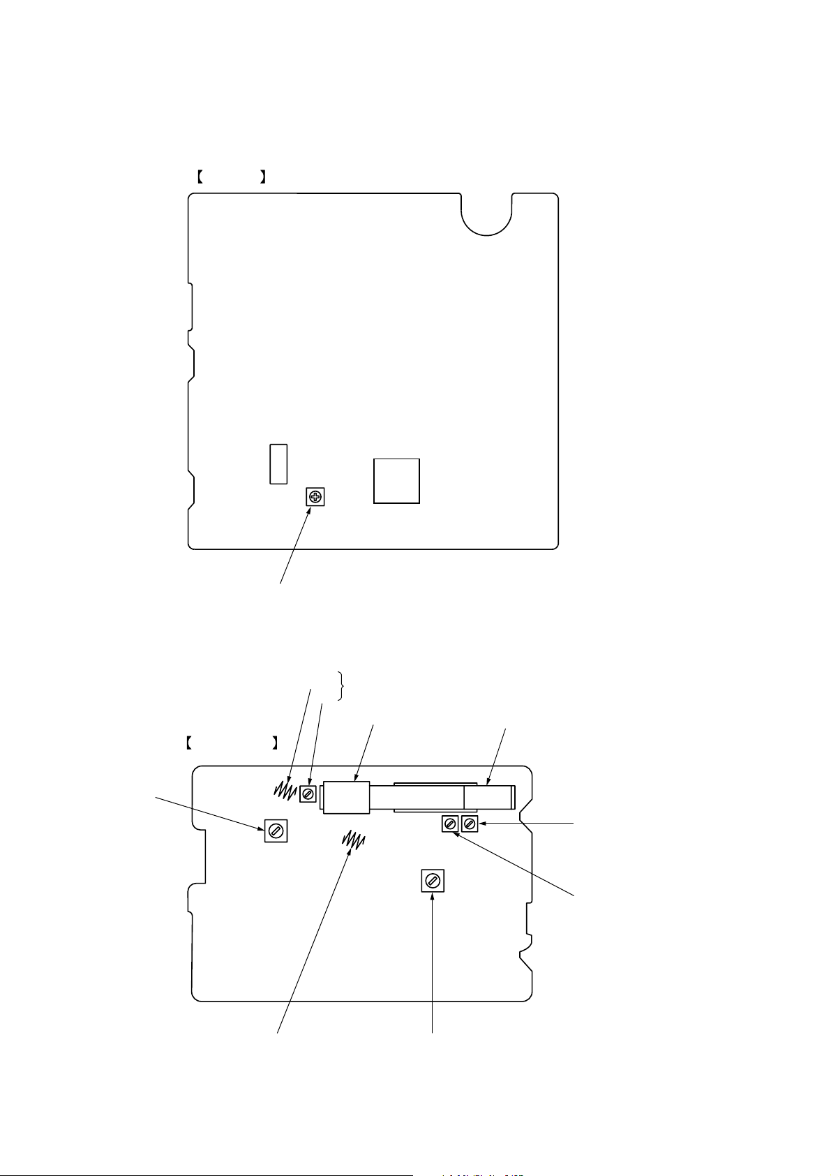
Adjustment Location :
CD BOARD
(SIDE A)
IC1007
IC1006
T1: MW/LW
IF Adjustment
RV1001:Focus Erorr Adjustment
L1
CT1
TUNER BOARD
(Component side)
FM Tracking Adjustment
L3: LW Tracking
Adjustment
(AEP, UK)
L3: MW Tracking
Adjustment
(AEP, UK)
CT5: LW Tracking
Adjustment
(AEP, UK)
CT3: AM (MW) Tracking
Adjustment
16
L2: FM Frequency
Coverage Adjustment
L4: AM Tracking Adjustment (US, CND, Korean, Taiwan
L4: LW Frequency Coverage Adjustment (AEP, UK)
SECTION 5
DIAGRAMS
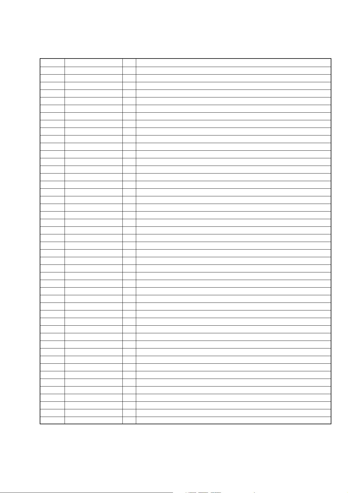
5-1. EXPLANATION OF IC TERMINALS
IC801 CXP83620-029Q SYSTEM CONTROL
Pin No. Pin name I/O Description
1 C-DOOR I Door open/close switch (S701) input
2 RMC I Remote control signal input
3 ES-EMG O Emergency signal output
4 B/C-MUTE O Radio mute signal output
5 REC-MUTE O Mute signal output on switching function
6 ES-CS I CD chip select signal input
7 ES-CLK I CD clock signal input
8 ES-ID I CD serial data signal input
9 ES-OD O CD serial data signal output
10 P-CON O Power control signal output
11 BATTCHK O Battery voltage check signal output
12 MP3LIGHT O MP3 light signal output
13 A-MUTE O Audio mute signal output
14 R-COUNT O Radio count signal output
15 R-CLOCK O Radio control clock signal output
16 R-DATA O Radio control data signal output
17 R-CE O Radio latch signal output
18 V-LATCH O Data latch signal output to LC75342 (VOL IC)
19 V-DATA O Data signal output to LC75342 (VOL IC)
20 V-CLOCK O Clock signal output to LC75342 (VOL IC)
21 AC/DC CHK I AC/DC check signal input
22 – 24 KEY-1 – 3 I Key input terminal of A/D port
25 VM REG I Battery center voltage input terminal of A/D port
26 VH REG I Battery voltage input terminal of A/D port
27 BL CONT/INIT O Initial setting signal and LCD back light control signal output
28 M. B/MODE CHECK I Reading specification and MEGA BASS signal input terminal (A/D port)
29 SHIFT CLOCK O Clock frequency shift change signal output
30 RST I System reset signal input
31 EXTAL I Crystal oscillator terminal (4.0MHz)
32 XTAL O Crystal oscillator terminal (4.0MHz)
33 VSS — Ground terminal
34 VL O LCD bias control signal output
35 VLC3 — LCD bias voltage terminal
36 VLC2 — LCD bias voltage terminal
37 VLC1 — LCD bias voltage terminal
38 – 41 COM0 – 3 O LCD common signal output
42 – 69 SEG0 – 27 O LCD segment signal output
70 RADIO O Radio function signal output
71 CD O CD function signal output
72 VDD — Power supply terminal
73 REC I Tape recording function signal input
74 NC — Not used (Connect to ground)
75 NC — Not used (Open)
76, 77 ISS-1, -2 O ISS select signal output
78 TC-PLAY I Tape play switch (S321) input
79 JOG + I JOG dial key (+) signal input
80 JOG – I JOG dial key (–) signal input
CFD-S40CP
17
CFD-S40CP
IC1001 ES3880 MP3 DECOMPRESSION
Pin No. Pin name I/O Description
1 VDD3 — Power supply terminal
2 RAS# O Strobe signal for M11B41256A (DRAM) column address output (Active: L)
3 DWE# O Write enable signal output to M11B41256A (DRAM) (Active: L)
4 – 12 DA0 – 8 O Address bus output to M11B41256A (DRAM)
13 – 28 DBUS0 – 15 I/O Data bus terminal to/from M11B41256A (DRAM)
29 RESET# I System reset signal input
30 VSS — Ground terminal
31 VDD3 — Power supply terminal
32 – 39 YUV0 – 7 O Not used (Open)
40 VSYNC I/O Not used (Open)
41 HSYNC I/O Not used (Open)
42 CPUCLK I System clock signal input from ES3889 (DSP)
43 PCLK2X I/O Clock for pixel double signal (27MHz)
44 PCLK I/O Clock for pixel signal (13.5MHz)
45 AUX0 I GFS signal input from CXD3068Q
46 AUX1 O FOK signal output
47 AUX2 O CD serial data signal output
48 AUX3 O CPU interface clock signal output to CXD3068Q
49 AUX4 O I data request signal output
50 VSS — Ground terminal
51 VDD3 — Power supply terminal
52 AUX6 O CD serial clock signal output
53 AUX5 O System data strobe signal output
54 AUX7 O CD serial chip select signal output
55 – 62 LD0 – 7 I/O Data bus to/from RISK interface
63 LWR# O Not used (Open)
64 LOE# O Output enable signal output to RISK interface
65 LCS3 O Chip enable signal output to HT27C020 (ROM)
66 LCS1 O Clock signal output to system data
67 LCS0 O Clock signal output to CXD3068Q (DSP)
68 – 79 LA0 – 11 I/O Address bus to/from HT27C020 (ROM)
80 VSS — Ground terminal
81 VPP — Protection voltage terminal
82 – 87 LA12 – 17 I/O Address bus to/from HT27C020 (ROM)
88 ACLK I/O Master clock signal of audio DAC data
89 AOUT/SEL-PLL0 I/O Serial data to/from audio interface
90 ATCLK O Transferring audio bit clock signal output
91 ATFS/SEL-PLL1 O Sync. signal output of transferring audio frame signal
92 DA9/DOE# O Output enable signal output to M11B41256A (DRAM)
93 AIN I Serial data input from audio interface
94 ARCLK I Bit clock signal input from audio receiver
95 ARFS I Frame sync. signal input from audio receiver
96 TDMCLK I Serial clock input from CXD3068Q
97 TDMDR I Serial data input from CXD3068Q
98 TDMFS I Frame sync. signal input from CXD3068Q
99 CAS# O Strobe signal for M11B41256A (DRAM) row address output (Active: L)
100 VSS — Ground terminal
18
 Loading...