

Page 1
CDX-V7800X
SERVICE MANUAL
Ver 1.1 2001.06
• The tuner and CD sections have no adjustments.
SPECIFICATIONS
E Model
Tourist Model
Model Name Using Similar Mechanism NEW
CD Drive Mechanism Type MG-383K-121//K
Optical Pick-up Name KSS-720A
CD player section
System Compact disc digital audio
system
Signal-to-noise ratio 90 dB
Frequency response 10 – 20,000 Hz
Wow and flutter Below measurable limit
Signal format system PAL/NTSC
Tuner section
FM
Tuning range FM tuning interval:
50 kHz/200 kHz
switchable
87.5 – 108 MHz
(at 50 kHz step)
87.5 – 107.9 MHz
(at 200 kHz step)
Aerial terminal External aerial connector
Intermediate frequency 10.7 MHz/450 kHz
Usable sensitivity 9 dBf
Selectivity 75 dB at 400 kHz
Signal-to-noise ratio 65 dB (stereo),
68 dB (mono)
Harmonic distortion at 1 kHz
0.7% (stereo),
0.4% (mono)
Separation 35 dB at 1 kHz
Frequency response 30 – 15,000 Hz
AM
Tuning range AM tuning interval:
9 kHz/10 kHz switchable
531 – 1,602 kHz
(at 9 kHz step)
530 – 1,710 kHz
(at 10 kHz step)
Aerial terminal External aerial connector
Intermediate frequency 10.7 MHz/450 kHz
Sensitivity 30 µV
Power amplifier section
Outputs Speaker outputs
(sure seal connectors)
Speaker impedance 4 – 8 ohms
Maximum power output 50 W × 4 (at 4 ohms)
General
Outputs Audio outputs
Video output
Power aerial relay control
lead
Power amplifier control
lead
Input Telephone ATT control
lead
Parking break control lead
Tone controls Bass ±9 dB at 100 Hz
Treble ±9 dB at 10 kHz
Power requirements 12 V DC car battery
(negative earth)
Dimensions Approx. 178 × 50 × 183 mm
(w/h/d)
Mounting dimensions Approx. 182 × 53 × 162 mm
(w/h/d)
Mass Approx. 1.2 kg
Supplied accessories Parts for installation and
connections (1 set)
Front panel case (1)
Card remote commander RM-X200
Design and specifications are subject to change without
notice.
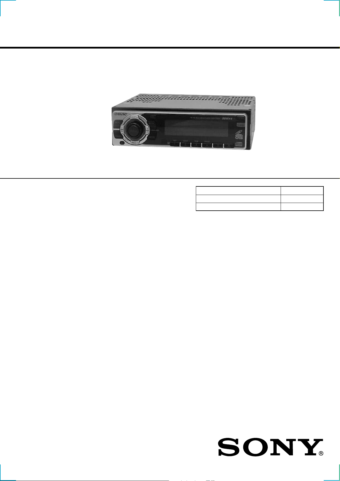
FM/AM MULTI MEDIA PLAYER
9-870-201-12
2001F0400-1
© 2001.6
Sony Corporation
e Vehicle Company
Shinagawa Tec Service Manual Production Group
1
Page 2

SERVICE NOTES
TABLE OF CONTENTS
NOTES ON HANDLING THE OPTICAL PICK-UP BLOCK
OR BASE UNIT
The laser diode in the optical pick-up block may suffer electrostatic
breakdown because of the potential difference generated by the
charged electrostatic load, etc. on clothing and the human body.
During repair, pay attention to electrostatic breakdown and also use
the procedure in the printed matter which is included in the repair
parts.
The flexible board is easily damaged and should be handled with
care.
NOTES ON LASER DIODE EMISSION CHECK
The laser beam on this model is concentrated so as to be focused on
the disc reflective surface by the objective lens in the optical pickup block. Therefore, when checking the laser diode emission, observe from more than 30 cm away from the objective lens.
Notes on Chip Component Replacement
• Never reuse a disconnected chip component.
• Notice that the minus side of a tantalum capacitor may be dam-
aged by heat.
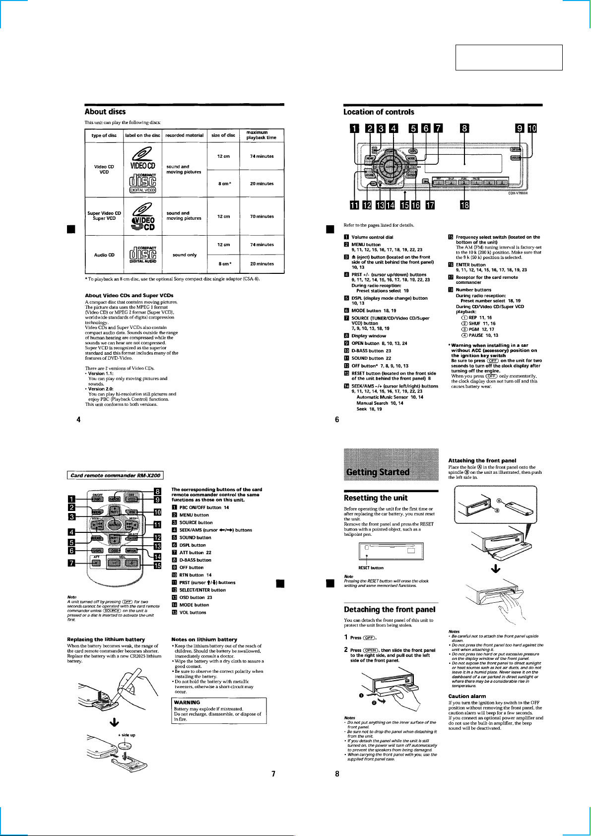
1. GENERAL
About Discs .............................................................................3
Location of Controls................................................................ 3
Getting Started......................................................................... 3
CD ........................................................................................... 4
Video CD/Super VCD ............................................................. 5
Radio ....................................................................................... 6
Other Functions .......................................................................6
MP3 File Instruction................................................................ 7
Connections ............................................................................. 9
2. DISASSEMBLY
2-1. Sub Panel (CD) Assy......................................................... 10
2-2. CD Mechanism Block ....................................................... 10
2-3. Main Board ....................................................................... 11
2-4. Heat Sink ........................................................................... 11
2-5. Chassis (T) Sub Assy ........................................................12
2-6. Lever Section..................................................................... 12
2-7. Servo Board....................................................................... 13
2-8. Shaft Roller Assy .............................................................. 13
2-9. Floating Block Assy .......................................................... 14
2-10. Optical Pick-up Block ....................................................... 14
3. DIAGRAMS
3-1. IC Pin Descriptions ...........................................................15
3-2. Block Diagram –Tuner Section–....................................... 23
3-3. Block Diagram –CD Section–........................................... 24
3-4. Block Diagram –MPEG Section– .....................................25
3-5. Block Diagram –Display Section–.................................... 26
3-6. Circuit Boards Location ....................................................26
3-7. Printed Wiring Board –CD Mechanism Section– .............28
3-8. Schematic Diagram –CD Mechanism Section (1/3)– .......30
3-9. Schematic Diagram –CD Mechanism Section (2/3)– .......31
3-10. Schematic Diagram –CD Mechanism Section (3/3)– .......32
3-11. Schematic Diagram –Main Section (1/2)– ........................ 33
3-12. Schematic Diagram –Main Section (2/2)– ........................ 34
3-13. Printed Wiring Board –Main Section– .............................. 35
3-14. Schematic Diagram –Relay Section–................................ 36
3-15. Printed Wiring Board –Relay Section– ............................. 37
3-16. Printed Wiring Board –Display Section– .......................... 38
3-17. Schematic Diagram –Display Section–............................. 39
SAFETY-RELATED COMPONENT WARNING!!
COMPONENTS IDENTIFIED BY MARK 0 OR DOTTED LINE
WITH MARK 0 ON THE SCHEMATIC DIAGRAMS AND IN
THE PARTS LIST ARE CRITICAL TO SAFE OPERATION.
REPLACE THESE COMPONENTS WITH SONY PARTS WHOSE
P ART NUMBERS APPEAR AS SHOWN IN THIS MANU AL OR
IN SUPPLEMENTS PUBLISHED BY SONY.
2
4. EXPLODED VIEWS
4-1. Chassis Section ................................................................. 42
4-2. Front Panel Section ...........................................................43
4-3. CD Mechanism Section (1) ............................................... 44
4-4. CD Mechanism Section (2) ............................................... 45
4-5. CD Mechanism Section (3) ............................................... 46
5. ELECTRICAL PARTS LIST ........................................47
Page 3
SECTION 1
GENERAL
This section extracted
from instruction manual.
3
Page 4
456
Page 5
Page 6
Page 7
MP3 FILE INSTRUCTION
7
Page 8
8
Page 9
CONNECTIONS
9
Page 10
6
SECTION 2
DISASSEMBLY
Note : Follow the disassembly procedure in the numerical order given.
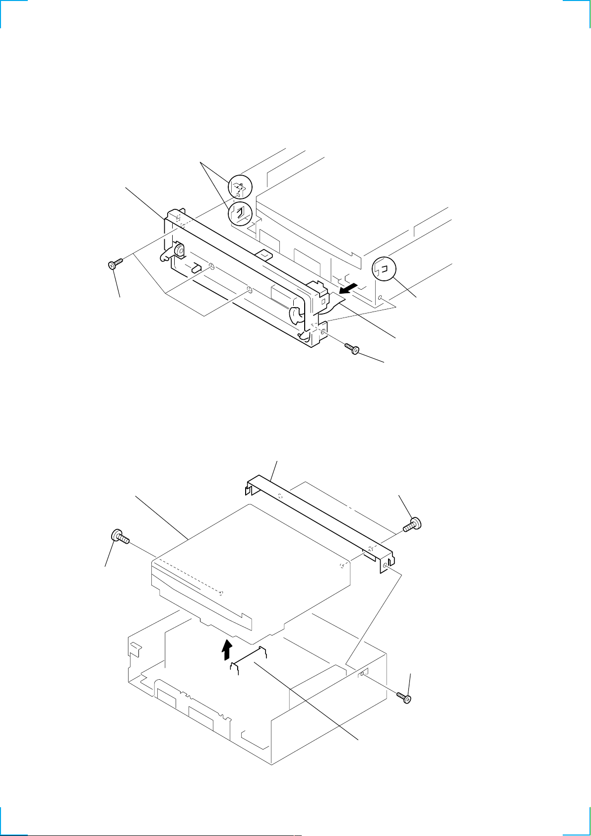
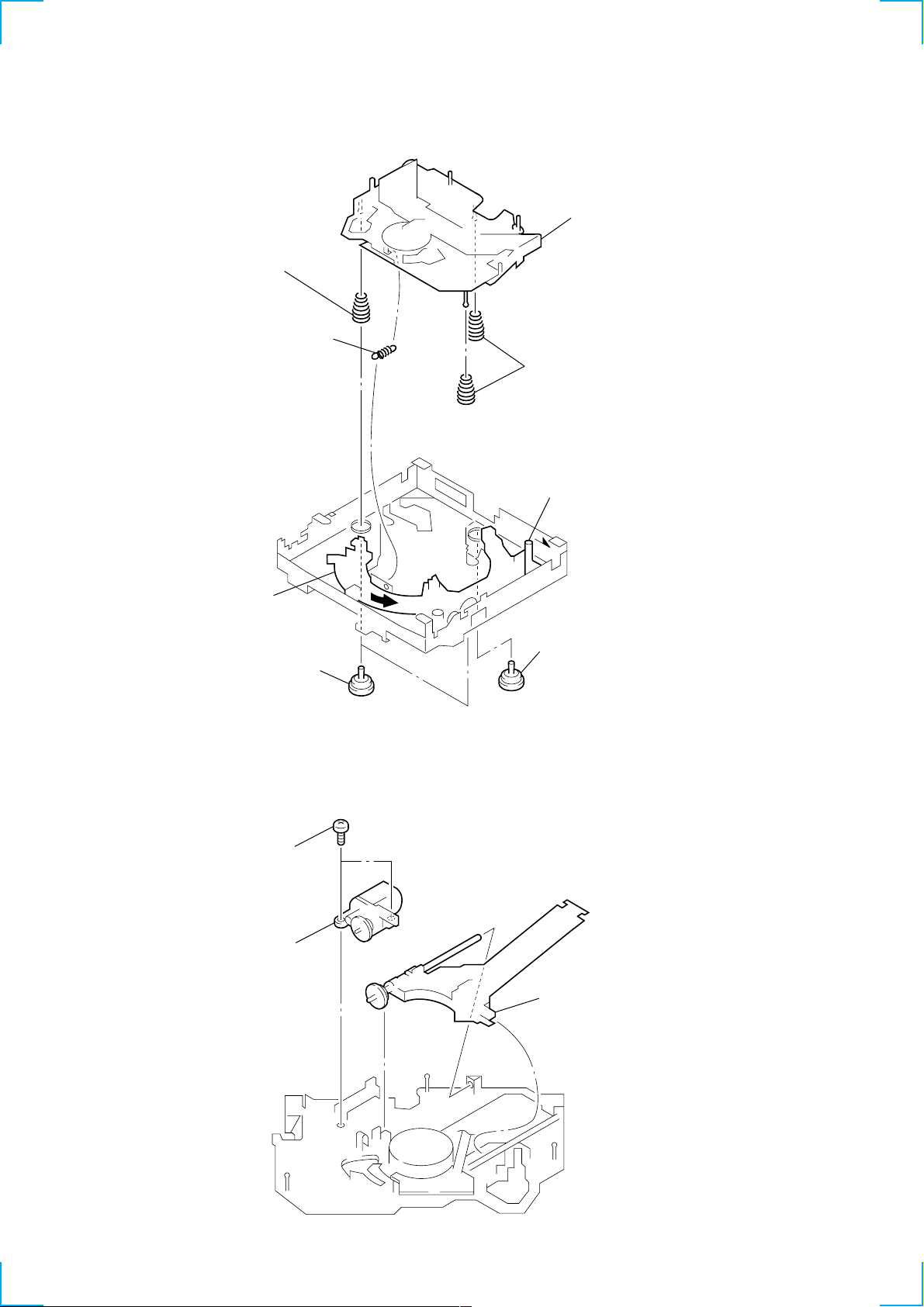
2-1. SUB PANEL (CD) ASSY
4 two claws
6 sub panel (CD) assy
2 PTT 2.6x6
2-2. CD MECHANISM BLOCK
5 CD mechanism block
2 PTT 2.6x6
3 claw
5 CNP800
1 PTT 2.6x6
7 bracket (CD)
6 PTT 2.6x6
10
3
4 CN701
1 PTT 2.6x
Page 11
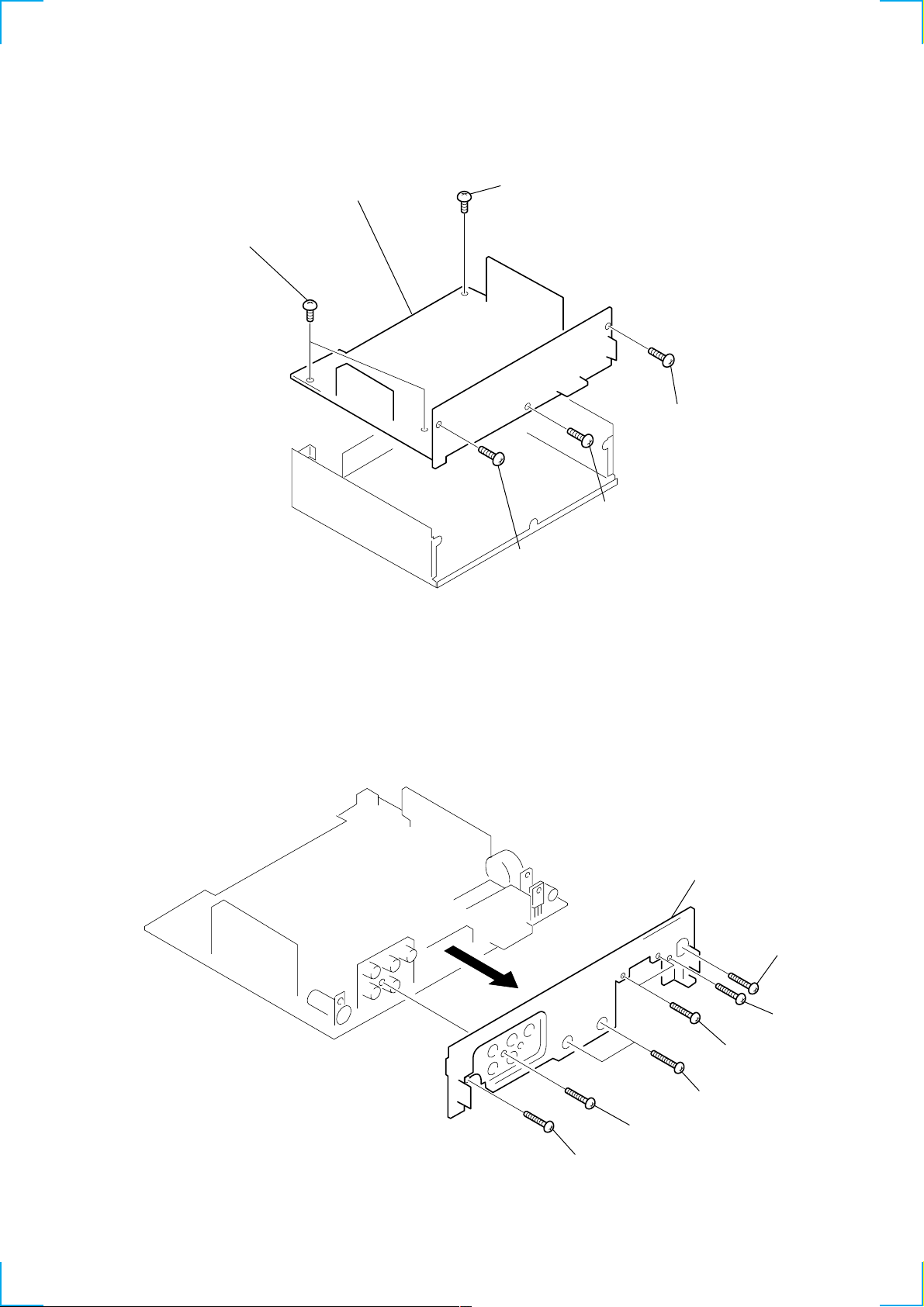
7 heat sink
1 PTT 2.6x8
2 PTT 2.6x8
4 PTT 2.6x8
5 PTT 2.6x8
3 PTT 2.6x12
6 PTT 2.6x8
8
2-3. MAIN BOARD
5 screws (BTT)
6 MAIN board
4 screws (BTT)
3 PTT 2.6x
2 PTT 2.6x8
1 PTT 2.6x8
2-4. HEAT SINK
11
Page 12
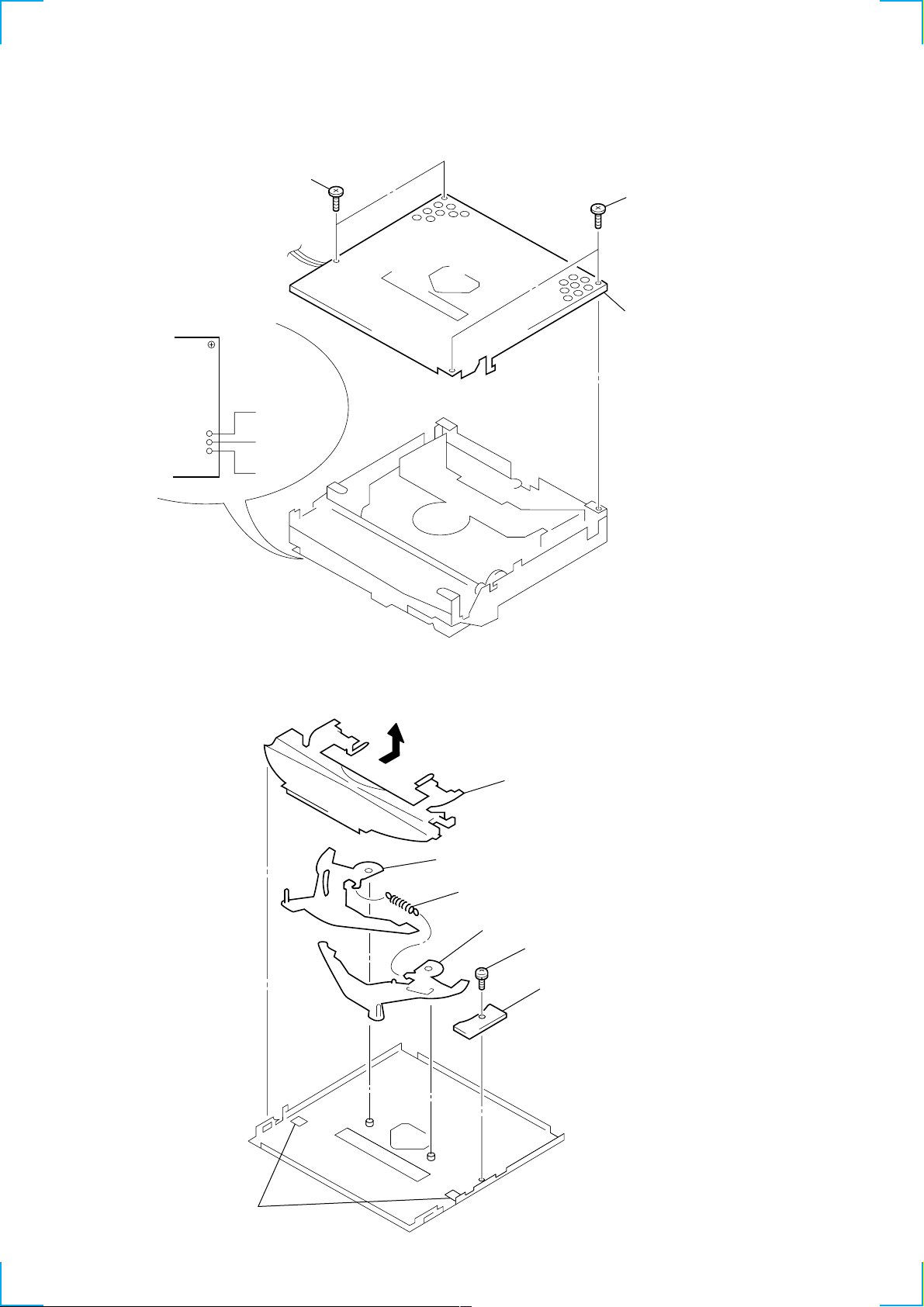
2-5. CHASSIS (T) SUB ASSY
2 P 2x3
3 P 2x3
1 Unsolder the
lead wires.
2-6. LEVER SECTION
4 chassis (T) sub assy
black
red
white
4
claws
6
lever (R)
3
tension spring (LR)
7
lever (L)
5
guide (disc)
1
special screw
2
DISC IN SW board
12
Page 13
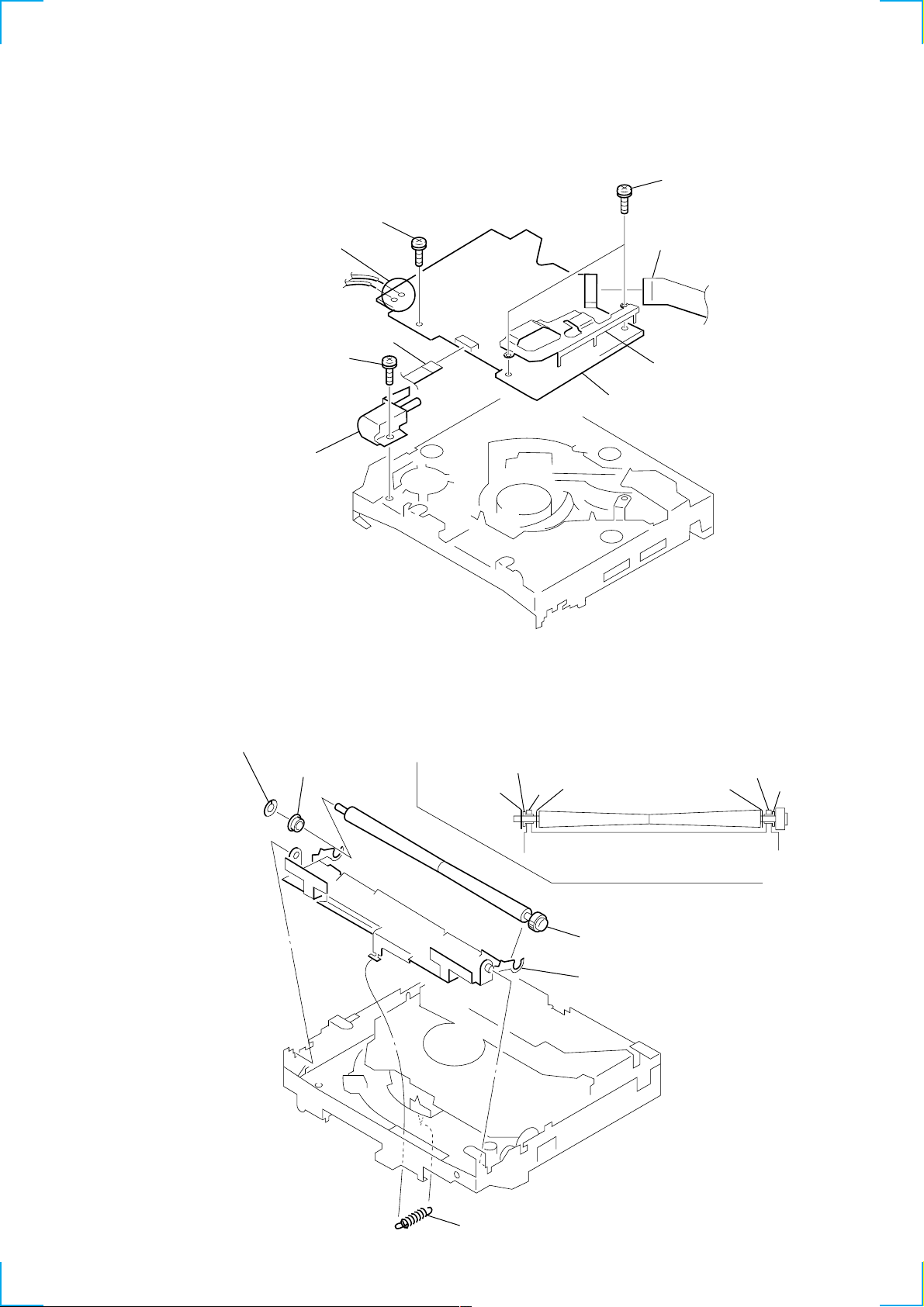
r
w
2-7. SERVO BOARD
3 Removal the solders.
6 Special screw
1 CN517
4 P 2x3
5 LO motor sub assy
(M903)
7 Special scre
2 CN518
8 heat sink (CD)
9 SERVO board
2-8. SHAFT ROLLER ASSY
3 retaing ring (RA)
4 shaft retainer
shaft retainer
retaing ring (RA)
washer
arm
washer
arm
shaft retaine
Fig. 1
5 shaft roller assy
2 arm (roller)
1 tension spring (RA)
13
Page 14
2-9. FLOATING BLOCK ASSY
7 compression spring (FL)
1 tension spring (KF1)
6 floating block assy
8 compression spring (FL)
4 Fit lever (D) in the
direction of the arrow.
5 Turn loading ring in the
direction of the arrow.
3 damper (T)
2-10. OPTICAL PICK-UP BLOCK
1 P 2x3
2 sled motor assy
(M902)
2 damper (T)
3 optical pick-up block
14
Page 15
SECTION 3
DIAGRAMS
3-1. IC PIN DESCRIPTIONS
• IC513 CXP81960M-659R (CD SYSTEM CONTROL)
Pin No. Pin Name I/O Pin Description
1 A MUTE O Audio mute control output
2 N.C — Not used. (Open)
3 CD ON O CD servo power supply control output
4 RW/R O RF amplifier gain control output (H: CD-RW, L: CD-R/CD-DA)
5 SLD MINUS O Sled motor control output
6 SELF SW I Disc self store switch input
7 E/(U) I Destination setting input (Fixed at H in this set)
8 PH1 I Photo coupler input 1 (Not used in this set)
9 SDA I/O I2C interface data input/output for video encoder IC.
10 SCL O I2C interface clock output to video encoder IC.
11 H WAIT I Wait input from MPEG decoder (Host) IC.
12 H INT I Interruption input from MPEG decoder IC.
13 – 20 HDATA7 – 0 I/O Host data 7 – 0 input for MPEG decoder IC.
21 EMPH O O D/A converter emphasis control output to DSP IC.
22 CD DATA O Data output to CD servo IC.
23 CD XTAL O System latch output to CD servo IC.
24 CD CKO O Clock output to CD servo IC.
25 D SW I Disc switch input
26 N.C — Not used. (Fixed at H in this set)
27 LIMIT SW I Sled limit switch input
28 SUBQ I CD sub-Q serial data input from DSP IC.
29 N.C — Not used. (Open)
30 SQCK O Sub-Q clock output to DSP IC.
31 N.C — Not used. (Open)
32 MSRQ O Serial request output of master microcomputer.
33 N.C — Not used. (Open)
34 CD RST O CD reset output
35, 36 N.C — Not used. (Open)
37 MP I Connect to VSS.
38 RESET I Slave microcomputer hard reset input
39 VSS — Ground
40 XTAL O Crystal oscillation output (12 MHz)
41 EXTAL I Crystal oscillation input (12 MHz)
42 N.C — Not used. (Fixed at H in this set)
43 TEXT IN I Not used. (Connect to SUBQ)
44 N.C — Not used. (Open)
45 TEXT CLK O Not used. (Connect to SQCK)
46 PH2 I Photo coupler input 2 (Not used in this set)
47 – 49 N.C — Not used. (Open)
50 AVSS — Analog ground
51 AVREF — Analog power supply reference input
52 AVDD — Analog power supply pin
53 GFS/MNT2 SEL I GFS/MNT2 select input of DSP IC. (Fixed at H in this set)
54 N.C — Not used. (Fixed at H in this set)
55 FOK I Focus OK input from DSP IC.
56 GFS I Guard frame synchro input from DSP IC.
57, 58 N.C — Not used. (Fixed at L in this set)
59 TEMP H I Not used. (Open)
60 TEMP L I Not used. (Open)
61 LOCK I Lock input from DSP IC.
62 TEST MODE I Not used. (Fixed at H in this set)
15
Page 16
Pin No. Pin Name I/O Pin Description
63 SENS I Sensitivity input from DSP IC.
64 IN SW I Disc in switch input
65, 66 N.C — Not used. (Fixed at H in this set)
67 MP3 I MP3 playback control input (H: not playback, L: playback)
68 PH3 I Photo coupler input 3 (Not used in this set)
69 SCLK O Serial clock output to DSP IC.
70 LM LOADING O Loading motor loading (CD tray close) output
71 TV RST O TV encoder IC reset output
72 N.C — Not used. (Open)
73 TE CANCEL O Tracking error offset cancel output of RF amplifier. (Not used in this set)
74 FE CANCEL O Focus error offset cancel output of RF amplifier. (Not used in this set)
75 BU IN I Back-up power supply input
76 SCOR I SCOR input from DSP IC.
77 MSO I Serial input from master microcomputer IC.
78 MSI O Serial output to master microcomputer IC.
79 MSC I Serial clock input from master microcomputer IC.
80 MCS I Chip select input from master microcomputer IC.
81 LM EJECT O Loading motor eject (CD tray open) output
82 DRV OE O Mute control output for driver IC.
83 MD2 O Check output for operation mode. (Not used in this set)
84 TEX I Not used. (Connect to VSS)
85 TX O not used. (Open)
86 VSS — Digital ground
87 VDD — Digital power supply pin
88 N.C — Not used. (Fixed at H in this set)
89 H R/W O Read/Write select output for MPEG decoder IC. (H: Read, L: Write)
90 H RD O Mode select output for MPEG decoder IC at read. (H: Multiflux, L: Individual)
91 – 93 HADDR2 – 0 O Host address 2 – 0 output for MPEG decoder IC.
94 H CS O Host chip select output for MPEG decoder IC.
95 N.C — Not used. (Open)
96 H RST O Host reset output
97 – 99 N.C — Not used. (Open)
100 CDM ON O CD mechanism deck loading motor power supply control output (8 V).
16
Page 17
• IC514 CL8830-PE0 (MPEG DECODER)
Pin No. Pin Name I/O Pin Description
1 RESERVED I Fixed at L in this set.
2 – 4 HDATA0 – 2 I/O 8-bit bi-directional host data bus 0 – 2 input/output
5 VDD — Power supply pin (+3.3 V)
6 HDATA3 I/O 8-bit bi-directional host data bus 3 input/output
7 VSS — Ground
8 – 11 HDATA4 – 7 I/O 8-bit bi-directional host data bus 4 – 7 input/output
12 VDD2.5 — Power supply pin (+2.5 V)
13 RESET I Hardware reset input
14 VSS — Ground
15 WAIT O Host wait output
16 INT O Host interrupt output
17 VDD — Power supply pin (+3.3 V)
18 NC O Not used. (Open)
19 VSS — Ground
20 – 26 NC O Not used. (Open)
27 VDD — Power supply pin (+3.3 V)
28 NC O Not used. (Open)
29 VSS — Ground
30 – 35 NC O Not used. (Open)
36 VDD — Power supply pin (+3.3 V)
37 NC O Not used. (Open)
38 VSS — Ground
39 NC O Not used. (Open)
40 VDD2.5 — Power supply pin (+2.5 V)
41 NC O Not used. (Open)
42 VSS — Ground
43 – 46 NC O Not used. (Open)
47 VDD — Power supply pin (+3.3 V)
48 NC O Not used. (Open)
49 VSS — Ground
50, 51 NC O Not used. (Open)
52 RESERVED I Fixed at L in this set.
53, 54 MDATA15, 0 I/O Memory data 15 and 0 input/output
55 VDD — Power supply pin (+3.3 V)
56 MDATA14 I/O Memory data 14 input/output
57 VSS — Ground
58 – 60 MDATA1, 13, 2 I/O Memory data 1, 13 and 2 input/output
61 VDD — Power supply pin (+3.3 V)
62 MDATA12 I/O Memory data 12 input/output
63 VSS — Ground
64 MDATA3 O I/O Memory data 3 input/output
65 VDD2.5 — Power supply pin (+2.5 V)
66 MDATA11 I/O Memory data 11 input/output
67 VSS — Ground
68 MDATA4 I/O Memory data 4 input/output
69 VDD — Power supply pin (+3.3 V)
70 MDATA10 I/O Memory data 10 input/output
71 VSS — Ground
72 – 74 MDATA5, 9, 6 I/O Memory data 5, 9 and 6 input/output
75 VDD — Power supply pin (+3.3 V)
76 MDATA8 I/O Memory data 8 input/output
77 VSS — Ground
17
Page 18
Pin No. Pin Name I/O Pin Description
78 MDATA7 I/O Memory data 7 input/output
79 LDQM O SDRAM LDQM output
80 UDQM O SDRAM UDQM output
81 VDD — Power supply pin (+3.3 V)
82 MWE O SDRAM write enable output
83 VSS — Ground
84 SD-CLK O SDRAM system clock output
85 SD-CAS O SDRAM column address output
86 SD-RAS O SDRAM row address output
87 VDD — Power supply pin (+3.3 V)
88 SD-CS1 O SDRAM bank select 1 output (Not used in this set)
89 VSS — Ground
90 SD-CS0 O SDRAM bank select 0 output
91 VDD2.5 — Power supply pin (+2.5 V)
92 NC O Not used. (Open)
93 VSS — Ground
94 NC O Not used. (Open)
95 VDD — Power supply pin (+3.3 V)
96 MADDR9 O Memory address 9 output
97 VSS — Ground
98 – 100 MADDR11, 8, 10 O Memory address 11, 8 and 10 output
101 VDD — Power supply pin (+3.3 V)
102 MADDR7 O Memory address 7 output
103 VSS — Ground
104 – 106 MADDR0, 6, 1 O Memory address 0, 6 and 1 output
107 VDD — Power supply pin (+3.3 V)
108 MADDR5 O Memory address 5 output
109 VSS — Ground
110 – 112 MADDR2, 4, 3 O Memory address 2, 4 and 3 output
113 VDD — Power supply pin (+3.3 V)
114 MADDR12 O Memory address 12 output
115 VSS — Ground
116 MADDR13 O Memory address 13 output
117 VDD2.5 — Power supply pin (+2.5 V)
118 MADDR14 O Memory address 14 output
119 VSS — Ground
120 – 122 MADDR15 – 17 O Memory address 15 – 17 output
123 VDD — Power supply pin (+3.3 V)
124 MADDR18 O Memory address 18 output
125 VSS — Ground
126, 127 MADDR19, 20 O Memory address 19 and 20 output
128 ROM-CS O ROM chip select output
129 RESERVED I Fixed at L in this set.
130 NC O Not used. (Open)
131, 132 GND — Ground
133 RESERVED I Fixed at L in this set.
134 VDD — Power supply pin (+3.3 V)
135 RESERVED I Fixed at L in this set.
136 VSS — Ground
137 – 141 RESERVED I Fixed at L in this set.
142, 143 VDATA0, 1 O Video data bus 0 and 1 output
144 VDD2.5 — Power supply pin (+2.5 V)
145 VDATA2 O Video data bus 2 output
18
Page 19

Pin No. Pin Name I/O Pin Description
146 VSS — Ground
147 RESERVED I Fixed at L in this set.
148 VDATA3 O Video data bus 3 output
149 VDD — Power supply pin (+3.3 V)
150 VDATA4 O Video data bus 4 output
151 VSS — Ground
152 VDATA5 O Video data bus 5 output
153 RESERVED I Fixed at L in this set.
154, 155 VDATA6, 7 O Video data bus 6 and 7 output
156 RESERVED I Fixed at L in this set.
157 HSYNC I/O Horizontal sync input/output
158 VSYNC I/O Vertical sync input/output
159 NC O Not used. (Open)
160 VDD — Power supply pin (+3.3 V)
161 NC O Not used. (Open)
162 VSS — Ground
163, 164 DA-DATA1, 2 O Serial audio samples relative to DA-BCK clock.
165 VDD2.5 — Power supply pin (+2.5 V)
166 DA-LRCK O PCM left-right clock output
167 DA-BCK O PCM bit clock output
168 VDD2.5 — Power supply pin (+2.5 V)
169 DA-XCK O Audio external frequency clock output
170 VSS — Ground
171 DAI-DATA I PCM input data, two channels.
172 DAI-LRCK I PCM input left-right clock
173 DAI-BCK I PCM input bit clock
174 RESERVED I Fixed at L in this set.
175 VDD — Power supply pin (+3.3 V)
176 A-VDD — Analog power supply pin (+3.3 V)
177 VCLK I Video clock input
178 SYSCLK I system clock input
179 A-VSS — Analog ground
180 CD-DATA I Serial CD data input
181 VDD — Power supply pin (+3.3 V)
182 CD-LRCK I Programmable polarity 16-bit word synchronization to the decoder (right channel HIGH).
183 VSS — Ground
184 CD-BCK I CD bit clock input
185 CD-C2PO I Asserted HIGH indicated a corrupted byte.
186 – 190 RESERVED I Fixed at L in this set.
191 NC O Not used. (Open)
192 RESERVED I Fixed at L in this set.
193 VDD — Power supply pin (+3.3 V)
194 NC O Not used. (Open)
195 VSS — Ground
196 VSS1 — Ground
197 VDD2.5 — Power supply pin (+2.5 V)
198 VSS1 — Ground
199 VSS — Ground
200 VSS1 — Ground
201 HOST8SEL I Host select input
202 – 204 HADDR0 – 2 I Host address bus 0 – 2 input
205 DTACKSEL I Data acknowledge select input
206 CS I Host chip select input
19
Page 20

Pin No. Pin Name I/O Pin Description
207 R/W I Read/write strobe input in I mode.
208 RD I Read strobe input in M mode.
20
Page 21

• IC801 µPD17708GC-618-3B9 (SYSTEM CONTROL)
Pin No. Pin Name I/O Pin Description
1 SIRCS I Wireless remote commander input
2 SELF SW I Self switch input
3 DOOR I Front panel open/close detection input
4 NOSE I Front panel with/without detection input
5NC— Not used. (Connect to ground)
6 SYSRST O Rest output for slave microcomputer IC.
7 DOOR IN O CD door open/close detection output
8 MUTE O Mute on/off control output
9, 10 NC — Not used. (Open)
11 BAND-SW I Initial setting switch input
12 AREA1-SW I Destination check input 1 (Fixed at L in this set)
13 AREA2-SW I Destination check input 2 (Fixed at H in this set)
14 NC — Not used. (Open)
15 PARK I Parking signal detection input
16 TEL MUTE I Attenuator on/off control input
17 POWER IC ON O Power supply control output to power amplifier IC.
18 SEEK O SEEK output
19 AMP MUTE O Output control to power amplifier IC.
20 NC — Not used. (Open)
21 GND3 — Ground
22 NC — Not used. (Connect to ground)
23, 24 KEYIN2, 1 I Key input of A/D converter.
25 ROT-IN I Rotary commander A/D value input
26 S-METER I S-meter input
27 TEST-SW I Initial setting switch input (Fixed at H in this set)
28 AM IFC I AM center frequency counter input
29 FM IFC I FM center frequency counter input
30 VDD2 — Power supply pin
31 VCOH FM I FM input at VCO is FM.
32 VCOL AM I AM input at VCO is AM.
33 GND2 — Ground
34 NC — Not used. (Open)
35 EO1 PDOUT O Error out output
36 TEST0 I Fixed at L in this set.
37, 38 NC — Not used. (Open)
39 LCL/DX O LOCAL/DX select output
40 BEEP O Beep output
41 ACC IN I Accessory input
42, 43 RE1, 2 I Rotary encoder input 1, 2
44 NC — Not used. (Open)
45 MONO O Monaural output (H: Monaural, L: Stereo)
46 SD I SD input
47 VOL CE O Chip enable output for Electric volume IC.
48 VOL CLK O Cloch output for Electric volume IC.
49 VOL DATA O Data output for Electric volume IC.
50 NC — Not used. (Open)
51 FM ON O FM system power control output (H: FM ON)
52 AM ON O AM system power control output (H: AM ON)
53 LCD CE O Chip enable output for LCD driver IC.
54 ILL ON O Front panel backlight control output (H: Illumination ON)
55 NC — Not used. (Connect to ground)
56, 57 NC — Not used. (Open)
21
Page 22

Pin No. Pin Name I/O Pin Description
58 ANT ON O Car antenna control output
59 EZ SEL I Rotary commander shift key input
60 POWER ON O System power on/off control and power amplifier control output
61 – 63 NC — Not used. (Open)
64 ST IN I FM stereo indicator input (L: FM STEREO ON, H: FM MONO ON)
65 LCD CK0 O Clock data output for LCD driver IC.
66 LCD SO O Serial data output for LCD driver IC.
67 NC — Not used. (Open)
68 MSC O Serial clock output to slave microcomputer IC.
69 MSI I Serial input from slave microcomputer IC.
70 MSO O Serial output to slave microcomputer IC.
71 MSRQ I Serial request input from slave microcomputer IC.
72 MCS O Chip select output to slave microcomputer IC.
73 NC — Not used. (Open)
74 VREF — Reference power supply voltage pin
75 GND1 — Ground
76 X OUT O Crystal oscillator output (4.5 MHz)
77 X IN I Crystal oscillator input (4.5 MHz)
78 BU IN I Back-up power supply input
79 VDD1 — Power supply pin
80 RESET I Reset input
22
Page 23

3-2. BLOCK DIAGRAM — TUNER SECTION —
CDX-V7800X
CNJ601
(ANTENNA)
2
MPEG
SECTION
(Page 25)
04
DRIVER 5V
MECHA ON
CD ON
AUDIO3.3V
D3.3V
1
2
AM ANT
FM ANT
TUNER UNIT
TU601
AM DET
ST IND
LCL/DX
S-METER
IFC/SEEK
Q905
Q901
(Page 25)
L-OUT
R-OUT
VT
VCO
MONO
SD
FM +B
TU +B
AM +B
REG
REG
18
16
12
22
4
5
6
11
19
20
21
8
9
10
9
MPEG
SECTION
1
CD
SECTION
(Page 24)
R-CH
AM POWER
CD MECHA
POWER CONTROL
Q906-908
CD POWER
CONTROL
Q902-904
VIDEO OUT
LOW PASS
FILTER
Q603,604
FM POWER
CONTROL
Q602,607
CONTROL
Q601,604
L-CH
BATT
BATT
POWER
CONTROL
Q909,923,924
3
MPEG
SECTION
(Page 25)
8
CD
SECTION
(Page 24)
36
37
38
SYSRST
SELF SW
MSC
MSI
MSO
MSRQ
MCS
BATT
64
39
35
31
32
28
26
46
29
51
52
68
69
70
71
72
6
2
ST IN
LCL/DX
PDOUT
VCOH FM
VCOL AM
AM IFC
S-METER
SD
FM IFC
FM ON
AM ON
MSC
MSI
MSO
MSRQ
MCS
SYSRST
SELF SW
ELECTRONIC VOLUME
28
27
SYSTEM CONTROL
IC801(1/2)
IC401
VOL CE
VOL DATA
VOL CLK
MUTE
BEEP
POWER ON
AMP MUTE
TEL MUTE
ACC IN
BU IN
ANT ON
AMP ON
23 22
47
49
48
8
40
17
19
16
41
78
58
60
TONE
CEDICL
18 17 16
A3.3V
FL
RL
21
,0
MPEG
SECTION
4
A MUTE
ACC CHECK
Q913,914
BU CHECK
Q911,912,922
VIDEO 6V
BU5V
REG
IC904
(Page 25)
MUTE DRIVE
Q401,402
ACC
BATT
BATT
BATT
Q405
1
5
Q406
BU CHECK
POWER SUPPLY
IC901
AMP ON
BU+B
5
AMP+B
VCC
IN2
12
IN1
11
AUX
16
IN
STBY MUTE
MPEG
SECTION
2
4
POWER AMP
IC902
4 22
(Page 25)
BATT
5
3
9
7
Q407
AM POWER
CONTROL
Q915,916
R-CH
R-CH
R-CH
BATT
ACC
PJ401-5
PJ401-3
PJ401-1
CNP901
10
11
12
13
16
-4
-2
1
9
2
3
4
6
5
7
VIDEO OUT
FRONT
AUDIO OUT
REAR
FL+
FL–
RL+
RL–
RR+
RR-
FR+
FR-
TEL MUTE
Signal path
: FM
: AM
: CD VIDEO
: CD AUDIO
ANT REM
AMP REM
BATT
ACC
23 23
Page 24

CDX-V7800X
3-3. BLOCK DIAGRAM — CD SECTION —
A
B
C
D
E
PD
04
OPTICAL PICK-UP
BLOCK
KSS-720A
I - V
CONV
F
LD
TRACKING
COIL
FOCUS
COIL
SPINDLE
MOTOR
LOADING
MOTOR
LD
DRIVE
Q511
M902
SLED MOTOR
TR+
TR–
F+
F–
M
M901
M
M903
M
A + B + C + D
A
6
B
7
C
8
D
9
A + C B + D
E
10
F
11
PD
2
LD
1
6
7
8
9
10
11
12
13
5
4
APC
DRIVER
IC512
SLED
MOTOR
DRIVE
TRACKING
COIL
DRIVE
FOCUS
COIL
DRIVE
SPINDLE
MOTOR
DRIVE
LOADING
MOTOR
DRIVE
NUTE1
NUTE2
RF AMP
IC511
31
32
25
24
22
21
18
1
2
34
35
VCA
A
+
B
+
C
+
D
COMP
COMP
EQ
AMP
AMP
SFDR
SRDR
TFDR
TRDR
FFDR
FRDR
RFAC
RFDC
RW/R
DSP
IC516
RFAC
6
23
FE
14
TE
16
12
61 92
RFDC
54
FE
50
52
53
38
39
40
41
42
43
35
TE
SE
MDP
A/D
CONV
SLED
SERVO
TRACKING
SERVO
FOCUS
SERVO
EFM
DEM
D/A
I/F
CLV
SERVO
SERIAL
I/F
PWM AMP
PWM
SUB CODE
PROCESSOR
CPU
I/F
FOK
AMP
XTAI
PCMDI
BCKI
LRCKI
PCMD
BCK
LRCK
C2PO
EMPHI
LOCK
GFS
SQSO
SQCK
SCOR
DATA
CLOCK
XLAT
SENS
SCLK
XRST
L-CH
1
TUNER
SECTION
(Page 23)
95
R-CH
86
80
82
78
79
81
77
23
84
34
22
6
7
24
13
15
14
16
17
32
11
IC515
CD SYSTEM CONTROL
EMPHO
21
61
LOCK
56
GFS
43
TEXT IN
28
SUBQ
SQCK
30
45
TEXT CLK
76
SCOR
22
CD DATA
24
CD CKO
CD XLAT
23
SENS
63
SCLK
69
FOK
55
RESET
38
81
LM EJECT
LM LOADING
70
4
RW/R
SLD MINUS
5
82
DRV OE
DA XCK
DA DATA
DA BCK
DA LRCK
CD PCMD
CD BCK
CD LRCK
CD C2PO
IC513(1/2)
SELF SW
IN SW
LIMIT
SW
D SW
MPEG
7
SECTION
(Page 25)
MPEG
6
SECTION
(Page 25)
SELF SW
6
64
27
25
SW1
(DOWN)
Signal path
: CD AUDIO
8
SW2
(SELF)
SW3
(DISC IN)
SW4
(LIMIT)
TUNER
SECTION
(Page 23)
2424
Page 25

3-4. BLOCK DIAGRAM — MPEG SECTION —
MPEG DECODER
IC514
CDX-V7800X
CD
SECTION
(Page 24)
CD PCMD
CD BCK
6
CD LRCK
CD C2P0
180
184
182
185
13
128
79
82
85
86
90
84
80
CD PCMD
CD BCK
CD LRCK
CD C2P0
RESET
ROM CS
LDQM
MWE
SD CAS
SD RAS
SD CSO
SD CLK
UDQM
MEMORY
CONTROL
MDATA 0-15
53,54,56,58-60
62,64,66,68,70
72-74,76
PROGRAM
STREAM
DEC
MADDR 0-18
CD-DA
DEC
MPEG
AUDIO
DEC
LYLICS
DEC
MPEG
AUDIO
DEC
OSD
DEC
HOST
I/F
H DATA 0-7
96,98-100,102,104-406
108,110-112,114,116
118,120-122,124
AUDIO
DSP
VIDEO
MIX
HADDR 0-2
2-4,6
8-10
DIGITAL
AUDIO
I/F
VDATA 0-7
202 - 204
HSYNC
VSYNC
VCLK
SYSCLK
R/W
WAITE
INT
CS
RD
163
167
166
169
154,155
142,143,145
148,150,152
157
158
177
178
206
207
208
15
16
IC519
X514
27MHz
DA DATA
DA BCK
DA LRCK
DA XCK
7
YCRCB
0-7
HSYNC
1
VSYNC
28
CKREF
24
CD SYSTEM CONTROL
94
H CS TV RST
H R/W
89
90
HRD
11
H WAITE
12
H INT
CD
SECTION
(Page 24)
DEMULTI-
PLEXER
SYNC
CTRL
IC513(2/2)
Y
CB-CY
RESET
SDA
SCL
CD ON
71
9
10
3
LUMA
PROCESS
CROMA
PROCESS
VIDEO DAC
IC518
CTRL
SDA
27 2625
SCL
DAC
VIDEO 5V
VIDEO AMP
IC551
11 1 4
7
POWER
CONTROL
Q513,514
CD ON
2
VIDEO OUT
9
TUNER
SECTION
(Page 23)
TUNER
MD 0-7
MA 0-18
H ADDR
0-2
91 - 93 2 - 913 - 20
CDM ON
100
MECHA ON
SECTION
(Page 23)
XTAL
EXTAL
MSC
MSI
MSO
MSRQ
MCS
RESET
A MUTE
BU IN
40
41
79
78
77
32
80
38
1
75
IC523
X511
12MHz
MSC
MSI
MSO
MSRQ
MCS
SYS RESET
A MUTE
BU CHECK
3
SECTION
(Page 23)
4
SECTION
5
SECTION
(Page 23)
TUNER
TUNER
(Page 23)
TUNER
Signal path
: CD VIDEO
HDATA
0-7
SDRAM
IC520
04
MD 0-15
2,3,5,6,8,9
11,12,39,40,42
43,45,46,48,49
DQ 0-15
LDQMWECAS
14 15 16 17 18 36
RASCSCLK
19-24
27-32
A0-10,BA
UDQM
MA 0-11
21-23
25-29
Q0-7
CE
3035
MD 0-7
1-6
9-20,31
A0-18
ROM
IC521
MA 0-11
96
H RESET
25 25
Page 26

d
CDX-V7800X
3-5. BLOCK DIAGRAM — DISPLAY SECTION —
SYSTEM CONTROL
IC801(2/2)
S802
(FREQUENCY SELECT)
FM50k/AM9k
FM200k/AM10k
S801
RESET
S803
(NOSE DET)
IR
RECEIVER
IC951
X801
4.5MHz
76
77
11
80
4
3
1
XOUT
XIN
BAND SW
RESET
NOSE
DOOR
SIRCS
LCD CE
LCD CKO
LCD SO
DOOR IN
ILL ON
KEY1
KEY2
3-6. CIRCUIT BOARDS LOCATION
LCD DRIVE
IC901
DISC IN SW board
53
65
66
BATT
7
BATT
54
24
23
CE
62
CL
63
DI
64
POWER
CONTROL
Q919,920
POWER
CONTROL
Q917,918,921
KEY MATRIX
LSW901-907,909-915
S901-904
S04-51
COM1-4
4-51
52-55
LCD901
LIQUID CRYSTAL
DISPLAY PANEL
RELAY board
DISPLAY board
LIMIT SW board
SERVO boar
MAIN board
tuner unit
(TU601)
CNP902
(REMOTE IN)
04
59
EZ SEL
25
ROT IN
RE1
RE2
42
43
LSW916
RE901
ROTARY
ENCODER
Z
2626
Page 27

THIS NOTE IS COMMON FOR PRINTED WIRING
BOARDS AND SCHEMATIC DIAGRAMS.
(In addition to this, the necessary note is
printed in each block.)
for schematic diagram:
• All capacitors are in µF unless otherwise noted. pF: µµF
50 WV or less are not indicated except for electrolytics
and tantalums.
• All resistors are in Ω and 1/
specified.
• % : indicates tolerance.
f
•
• C : panel designation.
Note: The components identified by mark 0 or dotted line
• U : B+ Line.
• Power voltage is dc 14.4V and fed with regulated dc power
• V oltages are taken with a V OM (Input impedance 10 MΩ).
• Waveforms are taken with a oscilloscope.
• Circled numbers refer to waveforms.
VIDEO TEST DISC: HLV-401 (TGIS-3)
Part No.: J-6095-031-A
Playback track No.: 34 (Full field color bar 75%)
• Signal path.
for printed wiring boards:
• X : parts extracted from the component side.
• Y : parts extracted from the conductor side.
•
• b : Pattern from the side which enables seeing.
Caution:
Pattern face side: Parts on the pattern face side seen from the
(Side B) pattern face are indicated.
Parts face side: Parts on the parts face side seen from the
(Side A) parts face are indicated.
: internal component.
with mark 0 are critical for safety.
Replace only with part number specified.
supply from ACC and BATT cords.
Voltage variations may be noted due to normal produc-
tion tolerances.
Voltage variations may be noted due to normal produc-
tion tolerances.
F : FM
f : AM
J : CD AUDIO
L : CD VIDEO
a
: Through hole.
(The other layer’s patterns are not indicated.)
4
W or less unless otherwise
• Waveforms (Servo board)
(MODE:CD PLAY)
1
0V
Approx. 200mVp-p
qf
(FE)
IC511
2
0V
Approx. 2Vp-p
qh
(TE)
IC511
3
0.8Vp-p
IC511
(RFDCO)
wd
4
4.8Vp-p
22.7µsec
IC516
(LRCK)
uj
5
4.8Vp-p
474nsec
ia
(BCK)
IC516
6
3.6Vp-p
16.9344MHz
2
(XCK)
IC515
7
3.2Vp-p
9
q;
qa
qs
qd
qf
qg
IC519
H
IC518
IC514
IC514 <znm
16.9344MHz
IC514 <zn.
IC514 <zmm
27MHz
4
(CVBS)
qa
(DA-LRCK)
<znn
DA-BCK
(
DA-XCK
(
27MHz
(VCLK)
1.5Vp-p
1Vp-p
3.5Vp-p
3.5Vp-p
)
2.2Vp-p
)
1.2Vp-p
3.5Vp-p
8
IC513
27 27
IC516
(MDP)
eg
12MHz
(EXTAL)
ra
7.6µsec
1Vp-p
IC514 <z,x
qh
IC514 <z,v
22.7µsec
(CD-LRCK)
3.2Vp-p
474nsec
(CD-BCK)
Page 28

CDX-V7800X
• Semiconductor Location
Ref. No. Location
(D511) B-5
D515 D-4
(D516) D-4
IC511 B-2
IC512 D-1
(IC513) F-6
IC514 C-7
IC515 F-4
IC516 F-2
IC518 F-7
(IC519) E-7
(IC520) B-7
(IC521) D-6
IC523 D-4
(IC551) D-5
(Q511) B-2
(Q513) D-4
(Q514) C-4
( ) : SIDE B
3-7. PRINTED WIRING BOARD — CD MECHANISM SECTION —
2828
Page 29

(Page 35)
CDX-V7800X
29 29
Page 30

CDX-V7800X
3-8. SCHEMATIC DIAGRAM — CD MECHANISM SECTION (1/3) — • Refer to page 27 for Waveforms. • Refer to page 40 for IC Block Diagrams.
Note:
• Voltage and waveforms are dc with respect to ground
under no-signal conditions.
no mark : VIDEO CD PLAY (Refer to page 27.)
: Impossible to measure
∗
(Page 31)
3030
Page 31

3-9. SCHEMATIC DIAGRAM — CD MECHANISM SECTION (2/3) — • Refer to page 27 for Waveforms. • Refer to page 40 for IC Block Diagrams.
(Page 30)
CDX-V7800X
(Page 33)
31 31
(Page 32)
Note:
• Voltage and waveforms are dc with respect to ground
under no-signal conditions.
no mark : VIDEO CD PLAY (Refer to page 27.)
( ) : AUDIO CD PLAY
: Impossible to measure
∗
Page 32

CDX-V7800X
3-10. SCHEMATIC DIAGRAM — CD MECHANISM SECTION (3/3) — • Refer to pag e 27 for Waveforms.
(Page 31)
Note:
• Voltage and waveforms are dc with respect to ground
under no-signal conditions.
no mark : VIDEO CD PLAY (Refer to page 27.)
( ) : AUDIO CD PLAY
3232
Page 33

3-11. SCHEMATIC DIAGRAM — MAIN SECTION (1/2) — • Refer to page 40 for IC Block Diagrams.
(Page 31)
CDX-V7800X
(Page 34)
Note:
• Voltage is dc with respect
to ground under no-signal
(detuned) condition.
no mark : FM
(): AM
< > : AUDIO CD PLAY
33 33
Page 34

CDX-V7800X
3-12. SCHEMATIC DIAGRAM — MAIN SECTION (2/2) — • Refer to page 36 for Waveforms. • Refer to page 40 for IC Block Diagrams.
(Page 33)
(Page 36)
Note:
• Voltage is dc with respect to
ground under no-signal
(detuned) condition.
no mark : FM
(): AM
< > : AUDIO CD PLAY
: Impossible to measure
∗
3434
Page 35

3-13. PRINTED WIRING BOARD — MAIN SECTION —
CDX-V7800X
LIGHT GREEN
PERK
(Page 29)
• Semiconductor Location
Ref. No. Location
D401 F-4
D402 D-6
D403 D-6
D407 C-11
D408 C-11
D409 F-7
D410 A-5
D602 F-2
D603 G-2
D604 I-2
D605 I-3
D801 J-3
D802 G-11
D803 J-2
D804 J-3
D805 K-5
D806 K-5
D807 J-3
D808 K-5
D809 K-5
D810 K-5
D902 H-12
D903 H-13
D904 I-13
D905 D-10
D908 I-11
D909 F-13
D910 F-12
D911 E-12
D912 E-12
D913 E-12
D914 G-12
D919 A-14
D920 A-13
D921 D-10
D922 J-13
D923 I-12
IC401 E-4
IC801 I-7
IC901 F-13
Ref. No. Location
IC902 A-8
IC903 C-14
IC904 G-12
Q401 E-6
Q402 E-6
Q403 C-5
Q404 C-4
Q405 B-3
Q406 C-4
Q407 D-9
Q601 G-3
Q602 G-3
Q603 D-3
Q604 E-3
Q606 H-3
Q607 H-2
Q901 B-13
Q902 A-12
Q903 H-11
Q904 G-11
Q905 G-13
Q906 H-13
Q907 I-13
Q908 I-12
Q909 D-11
Q911 I-11
Q912 I-11
Q913 F-11
Q914 F-12
Q915 F-11
Q916 E-11
Q917 J-12
Q918 J-12
Q919 J-10
Q920 K-10
Q921 I-13
Q922 I-11
Q923 E-11
Q924 F-10
(Page 37)
35 35
Page 36

CDX-V7800X
• Waveforms (Main board)
1
2.1Vp-p
4.5MHz
IC801
uh
3-14. SCHEMATIC DIAGRAM — RELAY SECTION —
(Page 39)
(Page 34)
3636
Page 37

3-15. PRINTED WIRING BOARD — RELAY SECTION —
CDX-V7800X
(Page 35)
37 37
(Page 38)
Page 38

CDX-V7800X
3-16. PRINTED WIRING BOARD — DISPLAY SECTION —
(Page 37)
• Semiconductor Location
Ref. No. Location
(D905) A-6
(D951) C-5
(IC901) B-8
IC951 C-6
LED910 B-12
( ) : SIDE B
Ref. No. Location
LED911 A-12
LED912 A-5
LED913 B-5
LED921 A-2
LED922 C-2
LED923 C-3
LED924 A-4
3838
Page 39

3-17. SCHEMATIC DIAGRAM — DISPLAY SECTION —
(Page 36)
CDX-V7800X
39 39
Note:
• Voltage is dc with respect to ground under no-signal
(detuned) condition.
no mark : FM
Page 40

• IC Block Diagrams.
IC511 CXA2570N-T4
1
LD
2
PD
3
EQ IN
4
AC SUM
5
GND
6
A
7
B
8
C
9
D
10
E
11
F
12
SW
APC
RW/ROM
(H/L)
AC
SUM
DC
SUM
RW/ROM
IC512 LA6556
MUTE2
MUTE1
VIN1/VREF SW
5V REG
+
–
–
+
GND
+
–
–
+
+
–
36
S-GND
35
MUTE2
34
MUTE1
VIN4
33
VIN4–
32
VIN4+
31
VREF-IN
30
VIN1 (VREF)-SW
29
VREF-OUT (CH1)
28
REG-OUT
27
REG-IN
26
VIN3+
25
VIN3–
24
IREF(CVSS)
24
RFDCI
23
VC
RW/ROM
RW/ROM
VC
RW/ROM
VC
RW/ROM
VCC
EQ
AC
VCA
RW/ROM
VC
VCC
RFDCO
22
VC
21
RFC
20
VFC
19
BST
18
RFG
17
VCC
16
TE
15
FEI
14
FE
13
RFAC
FWD
REV
VCC2
VL0–
VL0+
VO4+
VO4–
VO3+
VO3–
VO2+
VO2–
VO1+
VO1–
1
INPUT
2
3
4
5
6
7
8
9
10
11
12
13
OUTPUT
CONTROL
LEVEL
SHIFT
LEVEL
SHIFT
–
+
LEVEL
SHIFT
LEVEL
SHIFT
CH2-CH4 OUTPUT
ON/OFF
CH1 OUTPUT
ON/OFF
–
+
IC518 STV0119B
1
HSYNC
2
YCRCB7
3
YCRCB6
4
YCRCB5
5
YCRCB4
6
YCRCB3
7
YCRCB2
8
YCRCB1
9
YCRCB0
10
VSS
11
CVBS
12
VR CVBS
13
VSSA
14
IC401 LC75374E
CB-CR
Y
DEMULTIPLEXER
VDDA
9-BIT DAC
VSSA
RGB
ENCODING
PROCESSING
MACROVISION
7.0.1/6.1
CHROMA
PROCESSOR
SYNC CONTROL
LUMA
&
VIDEO TIMING
GENERATOR
AUTO TEST
COLOR BAR
PATTERN
CLOSED
CAPTIONS
CGMS
CSI2C
TRAP
CTRL+CFG
REGISTER
TELETEX
SWITCH AND
GAIN ADJUSTMENT
TTXS
CSI2C
VDDA
9-BIT TRIDAC
VSSA
28
27
26
25
24
23
22
21
20
19
18
17
16
15
VSYNC/
ODDEVEN
SDA
SCL
RESET
CKREF
TTXD
TTXS/
CSI2C
VDD
G/Y
R/C
B/CVBS
VR RGB
IREF(RGB)
VDDA
VC
IC 551 NJM2268V (TE2)
VOUT2
NC
VCC
VIN2
8 7 6 5
BIAS
CLAMP
1 2 3 4
VIN1
6.2dB
AMP
6.2dB
AMP
DRIVER
DRIVER
GND
75Ω
75Ω
VSAG1
VOUT1
VCC1
VIN1
VIN1–A
VIN1+A
VIN1–B
VIN3
14
15
16
AMP-A
–
+
17
–
18
+
AMP-B
–
+
–
+
23
VIN2+
22
+
–
VIN2–
21
20
19
VIN2
VIN1 +B
LSELO
L4
L3
L2
L1
VDD
R1
R2
R3
R4
RSELO
LVRIN
34
35
36
37
38
39
40
41
42
43
44
1
RVRIN
LCOM
+
–
–
+
+
–
+
–
–
+
–
+
2 345 6 7 8 9
RCOM
LT3
LT2
LT1
–
+
+
–
+
–
DECODER LATCH
+
–
RT1
RT2
RT3
LSIN
LTOUT
CONTROL
REGISTER
RSIN
RTOUT
NC
2627282930313233
SHIFT
NC
LSB2
LSB1
NC
2324
25
22
LFIN
+
–
+
+
–
10
11
NC
RSB1
RSB2
–
+
–
–
+
–
+
LFOUT
21
LROUT
20
19
VREF
18
CE
17
DI
16
CL
15
VSS
14
RROUT
RFOUT
13
12
RFIN
4040
Page 41

81
80
82
83
84
85
86
87
88
89
90
91
92
93
94
95
96
99
97
98
TIMING
LOGIC
CLOCK
GENERATOR
D/A
INTERFACE
DIGITAL
OUT
32k
RAM
ERROR
CORRECTOR
OVER SAMPLING
DIGITAL FILTER
3rd-ORDER
NOISE SHAPER
LOW-PASS
FILTER
VC
VC
DIGITAL
CLV
MIRR
DFCT
FOK
SERVO
AUTO
SEQUENCER
SERVO
INTERFACE
DIGITAL
PLL
EFM
DEMODULATOR
SUB CODE
PROCESSOR
CPU
INTERFACE
SERIAL-IN
INTERFACE
A/D
CONVERTER
OP AMP
ANALOG
SWITCH
PWM GENERATOR
79 78 77 76 75 74 73 72 71 70 69 68 67 66 65 64 63 62 61 60 59 58 57 56 55
ASYMMETRY
CORRECTOR
54 53 52 51
50
49
47
48
45
44
43
42
41
40
39
38
46
37
36
35
34
33
32
31
302928272625242322212019181716151413121110987654321
FOCUS PWM
GENERATOR
TRACKING PWM
GENERATOR
SLED PWM
GENERATOR
SERVO DSP
FOCUS SERVO
TRACKING
SERVO
SLED SERVO
INTERNAL BUS
PWM
100
LOW-PASS
FILTER
PWM
+
–
+
–
BCK
BCKI
ENPH
EMPHI
XVDD
XTAI
XTAO
XVSS
AVDD1
AOUT1
AIN1
LOUT1
AVSS1
AVSS2
LOUT2
AIN2
RMUT
AOUT2
AVDD2
LMUT
PCMDI
PCMD
LRCKI
LRCK
VDD
ASYE
DOUT
MD2
VSS
VPCO
V16M
VCTL
BIAS
AVDD3
PCO
FILI
FILO
CLTV
AVSS3
RFAC
ASYI
ASYO
AVDD0
IGEN
AVSS0
ADIO
RFDCCETE
SE
FE
VC
TES1
XTSL
VSS
VDD
FRDR
FFDR
TRDR
TFDR
SRDR
SFDR
TEST
FSTIO
SSTP
MDP
LOCK
PWMI
FOK
DFCT
VDD
VSS
MIRR
COUT
WDCK
C4M
SCOR
C2PO
GFS
XPCK
XUGF
WFCK
ATSK
SCKL
SENS
CLOK
XLAT
DATA
SYSM
XRST
EXCK
SBSO
SCSY
SQCK
SQSO
XOLT
SOCK
SOUT
VSS
VDD
IC516 CXD2598Q
IC901 BA4903ST-V5
5.7V
ON ON
AMPONAMP
+–
B+
THERMAL
SHUT
DOWN
CIRCUIT ON
GND VCC BU+B
+–
REGULATOR
VREF
OVER
VOLTAGE
PROTECT
51 2 3 4
41
Page 42

NOTE:
• The mechanical parts with no reference
number in the exploded views are not supplied.
• Items marked “*” are not stocked since
they are seldom required for routine service.
Some delay should be anticipated
when ordering these items.
• -XX and -X mean standardized parts, so
they may have some difference from the
original one.
4-1. CHASSIS SECTION
SECTION 4
EXPLODED VIEWS
• Color Indication of Appearance Parts
Example :
KNOB, BALANCE (WHITE) ... (RED)
R
Parts Color Cabinet’s Color
• Accessories and packing materials and
hardware (# mark) list are given in
the last of this parts list.
The components identified by
mark 0 or dotted line with mark
R
0 are critical for safety.
Replace only with part number
specified.
#2
9
MG-383K-121//K
8
11
15
10
16
14
13
#1
#1
#1
#2
#1
#3
#1
#1
#1
#1
12
TU601
4
3
19
#1
F901
11
2
1
5
#2
7
6
#5
#2
#5
#5
18
Ref. No. Part No. Description Remark
1 X-3378-387-2 PANEL (CD) ASSY, SUB
2 3-041-039-02 BUTTON (EJECT)
* 3 1-676-690-11 RELAY BOARD
4 X-3376-686-3 GEAR ASSY
5 3-030-909-02 DAMPER, OIL
6 X-3376-687-2 LOCK ASSY
7 3-713-786-51 SCREW +P 2X3
* 8 3-030-925-41 COVER
9 1-792-194-41 CORD (WITH CONNECTOR) (POWER)
* 10 3-041-173-01 BRACKET (CD)
11 3-922-535-11 SCREW (+BTT)
#2
#2
17
Ref. No. Part No. Description Remark
* 12 A-3283-013-A MAIN BOARD, COMPLETE
* 13 3-019-565-01 BRACKET (IC)
* 14 3-049-988-11 HEAT SINK (5P)
* 15 3-041-174-01 HEAT SINK (REG)
* 16 3-041-261-01 BRACKET (TR)
* 17 3-041-155-02 CHASSIS
18 3-035-250-02 SCREW (LOCK)
* 19 X-3376-689-2 BRACKET (GEAR) ASSY
F901 1-532-877-11 FUSE (BLADE TYPE) (AUTO FUSE) 10A
TU601 A-3220-779-A TUNER UNIT (TUX-010 (E))
42
Page 43

4-2. FRONT PANEL SECTION
#4
#4
57
#4
not supplied
(DISPLAY board)
55
66
65
LCD901
53
52
51
51 3-041-028-01 BUTTON (SOURCE)
52 3-041-029-02 KNOB (VOL)
53 3-041-030-62 BUTTON (CROSS)
54 3-042-967-02 CUSHION (CROSS)
* 55 X-3378-426-1 HOLDER (LCD) ASSY
54
64
63
61
62
59
58
56
Ref. No. Part No. Description RemarkRef. No. Part No. Description Remark
60 3-041-036-02 BUTTON (1-6/M)
61 3-042-984-02 BUTTON (MODE/ENTER)
62 3-041-035-02 BUTTON (OFF)
63 3-041-034-02 BUTTON (MENU/SOUND)
* 64 3-041-175-01 PLATE (LCD), GROUND
60
67
56 X-3379-260-2 PANEL (S) ASSY, FRONT
57 X-3378-391-1 PANEL ASSY, FRONT BACK
58 3-041-037-02 BUTTON (OPEN)
59 3-032-321-01 SPRING (OPEN)
65 1-694-660-11 CONDUCTIVE BOARD, CONNECTION
* 66 3-041-372-11 SHEET (REFLECTOR)
67 3-041-038-01 BUTTON (D)
LCD901 1-804-071-11 DISPLAY PANEL, LIQUID CRYSTAL
43
Page 44

4-3. CD MECHANISM SECTION (1)
(MG-383K-121//K)
101
115
104
114
109
116
103
#8
102
#8
107
106
105
117
118
114
113
C
M903
#7
105
C
110
111
112
108
119
#8
119
Ref. No. Part No. Description Remark Ref. No. Part No. Description Remark
* 101 1-676-709-11 DISC IN SW BOARD
102 3-040-039-02 CHASSIS (T)
103 3-040-038-01 SPRING (LR), TENSION
104 3-040-050-01 LEVER (L)
105 3-040-022-01 RETAINER (ROLLER), SHAFT
* 111 A-3283-016-A SERVO BOARD, COMPLETE
* 112 3-040-048-01 BRACKET (MOTOR)
113 3-040-034-01 SPRING (RA), TENSION
114 3-040-042-01 WASHER
115 3-043-880-01 RING (RA), RETAINING
106 3-040-044-01 ROLLER (S)
107 3-040-067-01 LEVER (R)
108 A-3301-980-A SHAFT ROLLER ASSY
109 3-040-037-01 GUIDE (DISC)
110 3-040-040-01 ARM (ROLLER)
44
116 3-044-206-11 SCREW, SPECIAL
* 117 3-223-249-01 SHEET (HEAT SINK)
* 118 3-223-248-01 HEAT SINK (CD)
119 3-044-206-51 SCREW, SPECIAL
M903 A-3315-039-A MOTOR SUB ASSY, LO (LOADING)
Page 45

4-4. CD MECHANISM SECTION (2)
(MG-383K-121//K)
157
158
162
163
154
D
160
165
151
156
157
164
155
153
161
D
159
152
152
152
Ref. No. Part No. Description Remark Ref. No. Part No. Description Remark
151 3-040-025-01 ARM, CHUCKING
152 3-040-031-01 DAMPER (T)
153 3-040-056-01 LEVER (D)
154 3-040-024-01 RETAINER (DISC)
155 3-040-053-01 RING, LOADING
159 A-3307-422-A CHASSIS (M) COMPLETE ASSY
160 3-040-059-01 SPRING (TR), TENSION
161 3-040-057-01 LEVER (LOCK)
162 3-040-058-01 GEAR (MDL)
163 3-040-052-01 WHEEL (U), WORM
156 3-040-026-01 SPRING (CH), TENSION
157 3-040-032-01 SPRING (FL), COMPRESSION
158 3-040-033-01 SPRING (KF1), TENSION
164 3-040-051-01 LEVER (TR)
165 3-040-054-01 WHEEL (LW), WORM
45
Page 46

4-5. CD MECHANISM SECTION (3)
(MG-383K-121//K)
207
201
M901
202
M902
208
203
#6
209
210
#8
204
205
206
Ref. No. Part No. Description Remark Ref. No. Part No. Description Remark
201 X-3378-480-1 CHASSIS (OP) ASSY (INCLUDING M901)
202 3-040-029-01 SPRING (SL), TORSION
203 3-040-045-01 BASE (DRIVING)
204 3-040-194-01 GEAR (MIDWAY)
205 A-3301-983-A SHAFT (FEED) ASSY
* 208 1-676-708-11 LIMIT SW BOARD
0 210 8-820-103-03 PICK-UP, OPTICAL KSS-720A/K1RP
211
#8
The components identified by
mark 0 or dotted line with mark
0 are critical for safety.
Replace only with part number
specified.
207 1-677-182-11 MOTOR FLEXIBLE BOARD
209 3-909-607-01 SCREW
211 3-040-030-01 SPRING (FEED), PLATE
206 1-676-707-11 PICK-UP FLEXIBLE BOARD
46
M902 A-3301-985-A MOTOR ASSY, SLED (SLED)
Page 47

SECTION 5
ELECTRICAL PARTS LIST
NOTE:
• Due to standardization, replacements in
the parts list may be different from the
parts specified in the diagrams or the
components used on the set.
• -XX and -X mean standardized parts, so
they may have some difference from the
original one.
• RESISTORS
All resistors are in ohms.
METAL:Metal-film resistor.
METAL OXIDE: Metal oxide-film resistor.
F:nonflammable
Ref. No. Part No. Description Remark Ref. No. Part No. Description Remark
* 1-676-709-11 DISC IN SW BOARD
****************
• Items marked “*” are not stocked since
they are seldom required for routine service.
Some delay should be anticipated
when ordering these items.
• SEMICONDUCTORS
In each case, u : µ, for example:
uA.. : µA.. uPA.. : µPA..
uPB.. : µPB.. uPC.. : µPC.. uPD.. : µPD..
• CAPACITORS
uF : µF
• COILS
uH : µH
LED923 8-719-078-83 LED SML-310VT (RING ILLUMINATION)
LED924 8-719-078-83 LED SML-310VT (RING ILLUMINATION)
DISC IN SW DISPLAY
The components identified by
mark 0 or dotted line with mark
0 are critical for safety.
Replace only with part number
specified.
When indicating parts by reference
number, please include the board.
< SWITCH >
SW2 1-529-566-21 SWITCH, PUSH (1 KEY) (SELF)
SW3 1-529-566-21 SWITCH, PUSH (1 KEY) (DISC IN)
*************************************************************
DISPLAY BOARD
**************
1-694-660-11 CONDUCTIVE BOARD, CONNECTION
* 3-041-175-01 PLATE (LCD), GROUND
* 3-041-372-11 SHEET (REFLECTOR)
< CAPACITOR >
C951 1-163-037-11 CERAMIC CHIP 0.022uF 10% 25V
C952 1-107-823-11 CERAMIC CHIP 0.47uF 10% 16V
C953 1-163-251-11 CERAMIC CHIP 100PF 5% 50V
< CONNECTOR >
CNP901 1-794-065-11 PLUG, CONNECTOR 14P
< DIODE >
D905 8-719-988-61 DIODE 1SS355TE-17
D951 8-719-420-90 DIODE MA8051-M-TX
< IC >
IC901 8-759-365-90 IC LC75824W
IC951 8-749-017-35 IC KSM-401N
< SWITCH >
LSW901 1-771-883-11 SWITCH, TACTILE (WITH LED) (OFF)
LSW902 1-771-476-11 SWITCH, KEY BOARD (WITH LED) (SOURCE)
LSW903 1-771-476-11 SWITCH, KEY BOARD (WITH LED) (SOUND)
LSW904 1-771-476-11 SWITCH, KEY BOARD (WITH LED) (MENU)
LSW905 1-771-476-11 SWITCH, KEY BOARD (WITH LED) (DSPL)
LSW906 1-771-476-11 SWITCH, KEY BOARD (WITH LED) (MODE)
LSW907 1-771-476-11 SWITCH, KEY BOARD (WITH LED) (ENTER)
LSW909 1-762-737-11 SWITCH, KEY BOARD (WITH LED) (D-BASS)
LSW910 1-771-883-11 SWITCH, TACTILE (WITH LED) (6)
LSW911 1-771-883-11 SWITCH, TACTILE (WITH LED) (5)
LSW912 1-771-883-11 SWITCH, TACTILE (WITH LED) (4/PAUSE)
LSW913 1-771-883-11 SWITCH, TACTILE (WITH LED) (3/PGM)
LSW914 1-771-883-11 SWITCH, TACTILE (WITH LED) (2/SHUF)
LSW915 1-771-883-11 SWITCH, TACTILE (WITH LED) (1/REP)
< RESISTOR >
R901 1-219-286-11 RES-CHIP 680 2% 1/16W
R902 1-219-286-11 RES-CHIP 680 2% 1/16W
R903 1-219-286-11 RES-CHIP 680 2% 1/16W
R904 1-218-847-11 RES-CHIP 1K 2% 1/16W
R905 1-218-851-11 RES-CHIP 1.5K 2% 1/16W
R906 1-218-851-11 RES-CHIP 1.5K 2% 1/16W
R907 1-218-855-11 RES-CHIP 2.2K 2% 1/16W
R908 1-218-859-11 RES-CHIP 3.3K 2% 1/16W
R909 1-218-863-11 RES-CHIP 4.7K 2% 1/16W
R910 1-218-867-11 RES-CHIP 6.8K 2% 1/16W
< JUMPER RESISTOR >
JR902 1-216-864-11 METAL CHIP 0 5% 1/16W
< LIQUID CRYSTAL DISPLAY >
LCD901 1-804-071-11 DISPLAY PANEL, LIQUID CRYSTAL
< DIODE >
LED910 8-719-078-19 LED LWA673-R1S2 (LCD BACK LIGHT)
LED911 8-719-078-19 LED LWA673-R1S2 (LCD BACK LIGHT)
LED912 8-719-078-19 LED LWA673-R1S2 (LCD BACK LIGHT)
LED913 8-719-078-19 LED LWA673-R1S2 (LCD BACK LIGHT)
LED921 8-719-078-83 LED SML-310VT (RING ILLUMINATION)
LED922 8-719-078-83 LED SML-310VT (RING ILLUMINATION)
R911 1-218-871-11 RES-CHIP 10K 2% 1/16W
R912 1-219-286-11 RES-CHIP 680 2% 1/16W
R913 1-219-286-11 RES-CHIP 680 2% 1/16W
R914 1-219-286-11 RES-CHIP 680 2% 1/16W
R915 1-218-847-11 RES-CHIP 1K 2% 1/16W
R916 1-218-851-11 RES-CHIP 1.5K 2% 1/16W
R917 1-218-851-11 RES-CHIP 1.5K 2% 1/16W
R918 1-218-855-11 RES-CHIP 2.2K 2% 1/16W
R919 1-218-859-11 RES-CHIP 3.3K 2% 1/16W
R920 1-218-863-11 RES-CHIP 4.7K 2% 1/16W
R921 1-216-029-00 METAL CHIP 150 5% 1/10W
R923 1-216-183-00 RES-CHIP 240 5% 1/8W
R925 1-216-029-00 METAL CHIP 150 5% 1/10W
R927 1-216-045-00 METAL CHIP 680 5% 1/10W
R933 1-216-027-00 METAL CHIP 120 5% 1/10W
47
Page 48

DISPLAY
Ref. No. Part No. Description Remark Ref. No. Part No. Description Remark
R935 1-216-864-11 METAL CHIP 0 5% 1/16W
R936 1-216-045-00 METAL CHIP 680 5% 1/10W
R938 1-216-049-11 RES-CHIP 1K 5% 1/10W
R939 1-216-049-11 RES-CHIP 1K 5% 1/10W
R951 1-218-482-11 RES-CHIP 430 5% 1/16W
R952 1-216-807-11 METAL CHIP 68 5% 1/16W
R953 1-216-821-11 METAL CHIP 1K 5% 1/16W
R954 1-216-821-11 METAL CHIP 1K 5% 1/16W
R955 1-216-821-11 METAL CHIP 1K 5% 1/16W
R956 1-216-821-11 METAL CHIP 1K 5% 1/16W
R957 1-216-850-11 METAL CHIP 270K 5% 1/16W
R958 1-216-821-11 METAL CHIP 1K 5% 1/16W
R959 1-216-821-11 METAL CHIP 1K 5% 1/16W
R960 1-216-821-11 METAL CHIP 1K 5% 1/16W
R961 1-216-857-11 METAL CHIP 1M 5% 1/16W
R970 1-218-288-11 RES-CHIP 300 5% 1/16W
R971 1-218-288-11 RES-CHIP 300 5% 1/16W
R980 1-218-288-11 RES-CHIP 300 5% 1/16W
R981 1-218-288-11 RES-CHIP 300 5% 1/16W
R999 1-216-864-11 METAL CHIP 0 5% 1/16W
LIMIT SW
< ROTARY ENCODER >
MAIN
< CAPACITOR >
C401 1-163-007-11 CERAMIC CHIP 680PF 10% 50V
C402 1-163-007-11 CERAMIC CHIP 680PF 10% 50V
C403 1-164-346-11 CERAMIC CHIP 1uF 16V
C404 1-164-346-11 CERAMIC CHIP 1uF 16V
C405 1-164-346-11 CERAMIC CHIP 1uF 16V
C406 1-164-346-11 CERAMIC CHIP 1uF 16V
C407 1-164-346-11 CERAMIC CHIP 1uF 16V
C408 1-124-584-00 ELECT 100uF 20% 10V
C409 1-164-346-11 CERAMIC CHIP 1uF 16V
C410 1-164-346-11 CERAMIC CHIP 1uF 16V
C411 1-164-346-11 CERAMIC CHIP 1uF 16V
C412 1-164-346-11 CERAMIC CHIP 1uF 16V
C413 1-164-182-11 CERAMIC CHIP 0.0033uF 10% 50V
C414 1-164-182-11 CERAMIC CHIP 0.0033uF 10% 50V
C415 1-163-037-11 CERAMIC CHIP 0.022uF 10% 25V
C416 1-163-037-11 CERAMIC CHIP 0.022uF 10% 25V
C417 1-124-233-11 ELECT 10uF 20% 16V
C418 1-124-233-11 ELECT 10uF 20% 16V
C419 1-164-492-11 CERAMIC CHIP 0.15uF 10% 16V
C420 1-164-492-11 CERAMIC CHIP 0.15uF 10% 16V
RE901 1-475-014-11 ENCODER, ROTARY
< SWITCH >
S901 1-771-884-11 SWITCH, TACTILE (WITH LED) (SEEK/AMS
– . m)
S902 1-771-884-11 SWITCH, TACTILE (WITH LED) (DISC +/PRST +)
S903 1-771-884-11 SWITCH, TACTILE (WITH LED) (SEEK/AMS
+ M >)
S904 1-771-884-11 SWITCH, TACTILE (WITH LED) (DISC –/PRST –)
*************************************************************
* 1-676-708-11 LIMIT SW BOARD
***************
< CONNECTOR >
CN13 1-770-347-21 CONNECTOR, FPC 6P
< SWITCH >
SW4 1-529-565-11 SWITCH, PUSH (1 KEY) (LIMIT)
*************************************************************
* A-3283-013-A MAIN BOARD, COMPLETE
*********************
* 3-019-565-01 BRACKET (IC)
* 3-041-174-01 HEAT SINK (REG)
* 3-041-261-01 BRACKET (TR)
* 3-049-988-11 HEAT SINK (5P)
7-685-793-09 SCREW +PTT 2.6X8 (S)
7-685-795-09 SCREW +PTT 2.6X12 (S)
C421 1-164-492-11 CERAMIC CHIP 0.15uF 10% 16V
C422 1-164-492-11 CERAMIC CHIP 0.15uF 10% 16V
C423 1-124-233-11 ELECT 10uF 20% 16V
C424 1-124-233-11 ELECT 10uF 20% 16V
C425 1-124-234-00 ELECT 22uF 20% 16V
C426 1-124-233-11 ELECT 10uF 20% 16V
C427 1-124-233-11 ELECT 10uF 20% 16V
C428 1-124-233-11 ELECT 10uF 20% 16V
C429 1-124-233-11 ELECT 10uF 20% 16V
C430 1-164-346-11 CERAMIC CHIP 1uF 16V
C431 1-126-382-11 ELECT 100uF 20% 16V
C432 1-164-344-11 CERAMIC CHIP 0.068uF 10% 25V
C435 1-163-251-11 CERAMIC CHIP 100PF 5% 50V
C436 1-163-251-11 CERAMIC CHIP 100PF 5% 50V
C437 1-163-251-11 CERAMIC CHIP 100PF 5% 50V
C438 1-163-251-11 CERAMIC CHIP 100PF 5% 50V
C439 1-163-037-11 CERAMIC CHIP 0.022uF 10% 25V
C440 1-164-346-11 CERAMIC CHIP 1uF 16V
C441 1-164-346-11 CERAMIC CHIP 1uF 16V
C442 1-164-346-11 CERAMIC CHIP 1uF 16V
C443 1-164-346-11 CERAMIC CHIP 1uF 16V
C444 1-164-346-11 CERAMIC CHIP 1uF 16V
C445 1-124-257-00 ELECT 2.2uF 20% 50V
C449 1-124-233-11 ELECT 10uF 20% 16V
C450 1-135-473-21 ELECT 3300uF 20% 16V
C601 1-163-235-11 CERAMIC CHIP 22PF 5% 50V
C602 1-163-023-00 CERAMIC CHIP 0.015uF 5% 50V
C603 1-163-037-11 CERAMIC CHIP 0.022uF 10% 25V
C604 1-164-161-11 CERAMIC CHIP 0.0022uF 10% 100V
C605 1-163-022-00 CERAMIC CHIP 0.012uF 10% 50V
48
C606 1-163-022-00 CERAMIC CHIP 0.012uF 10% 50V
Page 49

MAIN
Ref. No. Part No. Description Remark Ref. No. Part No. Description Remark
C607 1-164-004-11 CERAMIC CHIP 0.1uF 10% 25V
C608 1-124-234-00 ELECT 22uF 20% 16V
C609 1-163-021-11 CERAMIC CHIP 0.01uF 10% 50V
C610 1-124-234-00 ELECT 22uF 20% 16V
C611 1-163-021-11 CERAMIC CHIP 0.01uF 10% 50V
C923 1-163-038-11 CERAMIC CHIP 0.1uF 25V
C924 1-163-021-11 CERAMIC CHIP 0.01uF 10% 50V
C925 1-163-021-11 CERAMIC CHIP 0.01uF 10% 50V
C926 1-164-004-11 CERAMIC CHIP 0.1uF 10% 25V
C927 1-164-004-11 CERAMIC CHIP 0.1uF 10% 25V
C612 1-164-004-11 CERAMIC CHIP 0.1uF 10% 25V
C613 1-124-233-11 ELECT 10uF 20% 16V
C614 1-163-037-11 CERAMIC CHIP 0.022uF 10% 25V
C615 1-124-464-11 ELECT 0.22uF 20% 50V
C616 1-163-017-00 CERAMIC CHIP 0.0047uF 5% 50V
C617 1-163-037-11 CERAMIC CHIP 0.022uF 10% 25V
C618 1-124-234-00 ELECT 22uF 20% 16V
C619 1-124-233-11 ELECT 10uF 20% 16V
C701 1-128-057-11 ELECT 330uF 20% 6.3V
C702 1-164-346-11 CERAMIC CHIP 1uF 16V
C703 1-128-057-11 ELECT 330uF 20% 6.3V
C704 1-128-057-11 ELECT 330uF 20% 6.3V
C705 1-164-346-11 CERAMIC CHIP 1uF 16V
C800 1-124-584-00 ELECT 100uF 20% 10V
C801 1-163-009-11 CERAMIC CHIP 0.001uF 10% 50V
C802 1-163-009-11 CERAMIC CHIP 0.001uF 10% 50V
C803 1-164-222-11 CERAMIC CHIP 0.22uF 25V
C804 1-163-009-11 CERAMIC CHIP 0.001uF 10% 50V
C805 1-163-021-11 CERAMIC CHIP 0.01uF 10% 50V
C806 1-163-234-11 CERAMIC CHIP 20PF 5% 50V
C807 1-163-233-11 CERAMIC CHIP 18PF 5% 50V
C809 1-164-222-11 CERAMIC CHIP 0.22uF 25V
C811 1-163-038-11 CERAMIC CHIP 0.1uF 25V
C812 1-163-037-11 CERAMIC CHIP 0.022uF 10% 25V
C813 1-164-346-11 CERAMIC CHIP 1uF 16V
C814 1-163-009-11 CERAMIC CHIP 0.001uF 10% 50V
C815 1-163-009-11 CERAMIC CHIP 0.001uF 10% 50V
C816 1-163-037-11 CERAMIC CHIP 0.022uF 10% 50V
C901 1-124-234-00 ELECT 22uF 20% 16V
C902 1-163-038-11 CERAMIC CHIP 0.1uF 25V
C903 1-124-234-00 ELECT 22uF 20% 16V
C904 1-163-038-11 CERAMIC CHIP 0.1uF 25V
C905 1-124-234-00 ELECT 22uF 20% 16V
C906 1-163-038-11 CERAMIC CHIP 0.1uF 25V
C907 1-124-234-00 ELECT 22uF 20% 16V
C908 1-163-038-11 CERAMIC CHIP 0.1uF 25V
C909 1-164-004-11 CERAMIC CHIP 0.1uF 10% 25V
C910 1-126-382-11 ELECT 100uF 20% 16V
C911 1-126-160-11 ELECT 1uF 20% 50V
C912 1-163-038-11 CERAMIC CHIP 0.1uF 25V
C913 1-124-259-11 ELECT 4.7uF 20% 16V
C914 1-164-346-11 CERAMIC CHIP 1uF 16V
C915 1-110-654-11 DOUBLE LAYERS 0.047F 5.5V
C919 1-126-160-11 ELECT 1uF 20% 50V
C920 1-164-004-11 CERAMIC CHIP 0.1uF 10% 25V
C921 1-163-021-11 CERAMIC CHIP 0.01uF 10% 50V
C922 1-163-021-11 CERAMIC CHIP 0.01uF 10% 50V
C928 1-164-004-11 CERAMIC CHIP 0.1uF 10% 25V
< JACK >
CNJ601 1-793-598-11 JACK (ANTENNA)
< CONNECTOR >
CNP701 1-764-617-12 PIN, CONNECTOR (PC BOARD) 30P
CNP800 1-569-907-11 SOCKET, CONNECTOR 12P
CNP901 1-774-701-11 PIN, CONNECTOR 16P
< JACK >
CNP902 1-764-270-21 JACK, STEREO MINIATURE (DIA.3.5)
(REMOTE IN)
< SURGE ABSORBER >
CP601 1-803-335-21 ABSORBER, CHIP SURGE
< DIODE >
D401 8-719-988-61 DIODE 1SS355TE-17
D402 8-719-109-71 DIODE MTZJ-T-77-3.9A
D403 8-719-988-61 DIODE 1SS355TE-17
D407 8-719-923-91 DIODE MTZJ-T-77-16A
D408 8-719-049-38 DIODE 1N5404TU
D409 8-719-914-43 DIODE DAN202K-T-146
D410 8-719-422-64 DIODE MA8062-M-TX
D602 8-719-050-84 DIODE RB441QT-77
D603 8-719-050-84 DIODE RB441QT-77
D604 8-719-991-33 DIODE 1SS133T-77
D605 8-719-109-85 DIODE MTZJ-T-77-5.1B
D801 8-719-109-93 DIODE MTZJ-T-77-6.2B
D802 8-719-988-61 DIODE 1SS355TE-17
D803 8-719-109-93 DIODE MTZJ-T-77-6.2B
D804 8-719-109-93 DIODE MTZJ-T-77-6.2B
D805 8-719-109-93 DIODE MTZJ-T-77-6.2B
D806 8-719-109-93 DIODE MTZJ-T-77-6.2B
D807 8-719-109-93 DIODE MTZJ-T-77-6.2B
D808 8-719-109-93 DIODE MTZJ-T-77-6.2B
D809 8-719-109-93 DIODE MTZJ-T-77-6.2B
D810 8-719-109-93 DIODE MTZJ-T-77-6.2B
D902 8-719-929-15 DIODE MTZJ-T-77-9.1B
D903 8-719-109-93 DIODE MTZJ-T-77-6.2B
D904 8-719-929-15 DIODE MTZJ-T-77-9.1B
D905 8-719-422-94 DIODE MA8091-L-TX
D908 8-719-109-93 DIODE MTZJ-T-77-6.2B
D909 8-719-110-49 DIODE MTZJ-T-77-18A
D910 8-719-109-97 DIODE MTZJ-T-77-6.8B
D911 8-719-200-82 DIODE 11ES2-TA1B
49
Page 50

MAIN
Ref. No. Part No. Description Remark Ref. No. Part No. Description Remark
D912 8-719-200-82 DIODE 11ES2-TA1B
D913 8-719-200-82 DIODE 11ES2-TA1B
D914 8-719-200-82 DIODE 11ES2-TA1B
D919 8-719-422-64 DIODE MA8062-M-TX
D920 8-719-422-64 DIODE MA8062-M-TX
Q602 8-729-030-51 TRANSISTOR 2SA1515S-R-TP
Q603 8-729-120-28 TRANSISTOR 2SC2412K-T-146-R
Q604 8-729-120-28 TRANSISTOR 2SC2412K-T-146-R
Q606 8-729-027-43 TRANSISTOR DTC114EK-T146
Q607 8-729-027-43 TRANSISTOR DTC114EK-T146
D921 8-719-422-64 DIODE MA8062-M-TX
D922 8-719-921-80 DIODE MTZJ-T-77-11B
D923 8-719-110-49 DIODE MTZJ-T-77-18A
< FERRITE BEAD >
FB701 1-414-598-11 INDUCTOR, FERRITE BEAD
FB801 1-216-295-11 SHORT 0
< IC >
IC401 8-759-487-82 IC LC75374E
IC801 8-759-688-96 IC uPD17708GC-618-3B9
IC901 8-759-572-12 IC BA4903ST-V5
IC902 8-759-690-99 IC TA8268HS
IC903 8-759-710-88 IC NJM431U-TE2
IC904 8-759-447-94 IC NJU7201U32-TE1
< JUMPER RESISTOR >
JR106 1-216-295-11 SHORT 0
JR107 1-216-295-11 SHORT 0
JR108 1-216-295-11 SHORT 0
JR109 1-216-295-11 SHORT 0
JR111 1-216-295-11 SHORT 0
JR112 1-216-295-11 SHORT 0
JR122 1-216-295-11 SHORT 0
JR125 1-216-295-11 SHORT 0
JR127 1-216-295-11 SHORT 0
JR135 1-216-295-11 SHORT 0
JR138 1-216-295-11 SHORT 0
JR140 1-216-295-11 SHORT 0
Q901 8-729-019-00 TRANSISTOR 2SD2394-G
Q902 8-729-019-00 TRANSISTOR 2SD2394-G
Q903 8-729-901-05 TRANSISTOR DTA124EK-T146
Q904 8-729-027-43 TRANSISTOR DTC114EK-T146
Q905 8-729-019-00 TRANSISTOR 2SD2394-G
Q906 8-729-019-00 TRANSISTOR 2SD2394-G
Q907 8-729-901-05 TRANSISTOR DTA124EK-T146
Q908 8-729-027-43 TRANSISTOR DTC114EK-T146
Q909 8-729-015-11 TRANSISTOR 2SD1802FAST-TL
Q911 8-729-120-28 TRANSISTOR 2SC2412K-T-146-R
Q912 8-729-120-28 TRANSISTOR 2SC2412K-T-146-R
Q913 8-729-027-43 TRANSISTOR DTC114EK-T146
Q914 8-729-027-43 TRANSISTOR DTC114EK-T146
Q915 8-729-027-52 TRANSISTOR DTC124EK-T146
Q916 8-729-101-07 TRANSISTOR 2SB798-T1-DLDK
Q917 8-729-027-43 TRANSISTOR DTC114EK-T146
Q918 8-729-901-05 TRANSISTOR DTA124EK-T146
Q919 8-729-027-43 TRANSISTOR DTC114EK-T146
Q920 8-729-216-22 TRANSISTOR 2SA1037K-T-146-S
Q921 8-729-019-00 TRANSISTOR 2SD2394-G
Q922 8-729-027-52 TRANSISTOR DTC124EK-T146
Q923 8-729-901-05 TRANSISTOR DTA124EK-T146
Q924 8-729-027-43 TRANSISTOR DTC114EK-T146
< RESISTOR >
R401 1-216-073-00 METAL CHIP 10K 5% 1/10W
R402 1-216-073-00 METAL CHIP 10K 5% 1/10W
R403 1-216-081-00 METAL CHIP 22K 5% 1/10W
R404 1-216-081-00 METAL CHIP 22K 5% 1/10W
R405 1-216-059-00 METAL CHIP 2.7K 5% 1/10W
< COIL >
L701 1-410-521-11 INDUCTOR 100uH
L901 1-419-476-31 COIL, CHOKE 250uH
< JACK >
PJ401 1-794-621-11 JACK, PIN (AUDIO OUT REAR/FRONT,
< TRANSISTOR >
Q401 8-729-027-52 TRANSISTOR DTC124EK-T146
Q402 8-729-901-05 TRANSISTOR DTA124EK-T146
Q403 8-729-920-21 TRANSISTOR DTC314TK-T-146
Q404 8-729-920-21 TRANSISTOR DTC314TK-T-146
Q405 8-729-920-21 TRANSISTOR DTC314TK-T-146
Q406 8-729-920-21 TRANSISTOR DTC314TK-T-146
Q407 8-729-120-28 TRANSISTOR 2SC2412K-T-146-R
Q601 8-729-030-51 TRANSISTOR 2SA1515S-R-TP
VIDEO OUT)
R406 1-216-059-00 METAL CHIP 2.7K 5% 1/10W
R407 1-216-033-00 METAL CHIP 220 5% 1/10W
R408 1-216-033-00 METAL CHIP 220 5% 1/10W
R409 1-216-033-00 METAL CHIP 220 5% 1/10W
R410 1-216-033-00 METAL CHIP 220 5% 1/10W
R411 1-216-081-00 METAL CHIP 22K 5% 1/10W
R412 1-216-081-00 METAL CHIP 22K 5% 1/10W
R413 1-216-081-00 METAL CHIP 22K 5% 1/10W
R414 1-216-081-00 METAL CHIP 22K 5% 1/10W
R415 1-216-049-11 RES-CHIP 1K 5% 1/10W
R416 1-216-089-11 RES-CHIP 47K 5% 1/10W
R417 1-216-077-00 RES-CHIP 15K 5% 1/10W
R418 1-216-077-00 RES-CHIP 15K 5% 1/10W
R419 1-216-077-00 RES-CHIP 15K 5% 1/10W
R420 1-216-077-00 RES-CHIP 15K 5% 1/10W
R421 1-216-105-00 RES-CHIP 220K 5% 1/10W
R426 1-216-089-11 RES-CHIP 47K 5% 1/10W
R427 1-216-089-11 RES-CHIP 47K 5% 1/10W
50
Page 51

MAIN
Ref. No. Part No. Description Remark Ref. No. Part No. Description Remark
R428 1-216-089-11 RES-CHIP 47K 5% 1/10W
R429 1-216-089-11 RES-CHIP 47K 5% 1/10W
R430 1-216-049-11 RES-CHIP 1K 5% 1/10W
R431 1-216-085-00 METAL CHIP 33K 5% 1/10W
R432 1-216-073-00 METAL CHIP 10K 5% 1/10W
R828 1-216-105-00 RES-CHIP 220K 5% 1/10W
R829 1-216-105-00 RES-CHIP 220K 5% 1/10W
R830 1-216-073-00 METAL CHIP 10K 5% 1/10W
R831 1-216-105-00 RES-CHIP 220K 5% 1/10W
R832 1-216-073-00 METAL CHIP 10K 5% 1/10W
R433 1-216-073-00 METAL CHIP 10K 5% 1/10W
R434 1-216-121-11 RES-CHIP 1M 5% 1/10W
R601 1-216-025-11 RES-CHIP 100 5% 1/10W
R602 1-216-061-00 METAL CHIP 3.3K 5% 1/10W
R603 1-216-025-11 RES-CHIP 100 5% 1/10W
R604 1-216-057-00 METAL CHIP 2.2K 5% 1/10W
R605 1-216-057-00 METAL CHIP 2.2K 5% 1/10W
R606 1-216-081-00 METAL CHIP 22K 5% 1/10W
R607 1-216-081-00 METAL CHIP 22K 5% 1/10W
R608 1-216-049-11 RES-CHIP 1K 5% 1/10W
R609 1-216-097-11 RES-CHIP 100K 5% 1/10W
R610 1-216-109-00 METAL CHIP 330K 5% 1/10W
R611 1-216-117-00 METAL CHIP 680K 5% 1/10W
R612 1-216-049-11 RES-CHIP 1K 5% 1/10W
R613 1-216-097-11 RES-CHIP 100K 5% 1/10W
R614 1-216-049-11 RES-CHIP 1K 5% 1/10W
R615 1-216-073-00 METAL CHIP 10K 5% 1/10W
R616 1-216-049-11 RES-CHIP 1K 5% 1/10W
R617 1-249-421-11 CARBON 2.2K 5% 1/4W
R618 1-216-057-00 METAL CHIP 2.2K 5% 1/10W
R620 1-216-073-00 METAL CHIP 10K 5% 1/10W
R701 1-216-295-11 SHORT 0
R801 1-216-081-00 METAL CHIP 22K 5% 1/10W
R802 1-216-081-00 METAL CHIP 22K 5% 1/10W
R803 1-216-097-11 RES-CHIP 100K 5% 1/10W
R833 1-216-105-00 RES-CHIP 220K 5% 1/10W
R834 1-216-105-00 RES-CHIP 220K 5% 1/10W
R835 1-216-025-11 RES-CHIP 100 5% 1/10W
R836 1-216-025-11 RES-CHIP 100 5% 1/10W
R837 1-216-025-11 RES-CHIP 100 5% 1/10W
R838 1-216-025-11 RES-CHIP 100 5% 1/10W
R839 1-216-105-00 RES-CHIP 220K 5% 1/10W
R840 1-216-105-00 RES-CHIP 220K 5% 1/10W
R841 1-216-049-11 RES-CHIP 1K 5% 1/10W
R842 1-216-073-00 METAL CHIP 10K 5% 1/10W
R843 1-249-417-11 CARBON 1K 5% 1/4W
R844 1-249-417-11 CARBON 1K 5% 1/4W
R845 1-216-105-00 RES-CHIP 220K 5% 1/10W
R848 1-216-033-00 METAL CHIP 220 5% 1/10W
R849 1-216-025-11 RES-CHIP 100 5% 1/10W
R850 1-249-417-11 CARBON 1K 5% 1/4W
R852 1-216-057-00 METAL CHIP 2.2K 5% 1/10W
R853 1-216-049-11 RES-CHIP 1K 5% 1/10W
R854 1-216-049-11 RES-CHIP 1K 5% 1/10W
R855 1-216-049-11 RES-CHIP 1K 5% 1/10W
R857 1-216-025-11 RES-CHIP 100 5% 1/10W
R858 1-216-025-11 RES-CHIP 100 5% 1/10W
R860 1-216-105-00 RES-CHIP 220K 5% 1/10W
R861 1-216-049-11 RES-CHIP 1K 5% 1/10W
R862 1-216-295-11 SHORT 0
R804 1-216-073-00 METAL CHIP 10K 5% 1/10W
R805 1-216-105-00 RES-CHIP 220K 5% 1/10W
R806 1-216-089-11 RES-CHIP 47K 5% 1/10W
R807 1-216-049-11 RES-CHIP 1K 5% 1/10W
R808 1-216-025-11 RES-CHIP 100 5% 1/10W
R809 1-216-049-11 RES-CHIP 1K 5% 1/10W
R810 1-216-025-11 RES-CHIP 100 5% 1/10W
R811 1-249-417-11 CARBON 1K 5% 1/4W
R812 1-249-417-11 CARBON 1K 5% 1/4W
R813 1-249-417-11 CARBON 1K 5% 1/4W
R814 1-216-049-11 RES-CHIP 1K 5% 1/10W
R815 1-216-105-00 RES-CHIP 220K 5% 1/10W
R816 1-249-417-11 CARBON 1K 5% 1/4W
R817 1-216-025-11 RES-CHIP 100 5% 1/10W
R818 1-216-049-11 RES-CHIP 1K 5% 1/10W
R819 1-216-025-11 RES-CHIP 100 5% 1/10W
R820 1-216-025-11 RES-CHIP 100 5% 1/10W
R821 1-216-025-11 RES-CHIP 100 5% 1/10W
R822 1-216-025-11 RES-CHIP 100 5% 1/10W
R823 1-216-025-11 RES-CHIP 100 5% 1/10W
R824 1-216-295-11 SHORT 0
R826 1-216-295-11 SHORT 0
R827 1-216-025-11 RES-CHIP 100 5% 1/10W
R863 1-216-049-11 RES-CHIP 1K 5% 1/10W
R864 1-216-049-11 RES-CHIP 1K 5% 1/10W
R865 1-216-049-11 RES-CHIP 1K 5% 1/10W
R866 1-216-049-11 RES-CHIP 1K 5% 1/10W
R867 1-216-049-11 RES-CHIP 1K 5% 1/10W
R868 1-216-025-11 RES-CHIP 100 5% 1/10W
R869 1-216-025-11 RES-CHIP 100 5% 1/10W
R870 1-216-033-00 METAL CHIP 220 5% 1/10W
R871 1-249-437-11 CARBON 47K 5% 1/4W
R902 1-249-413-11 CARBON 470 5% 1/4W
R903 1-216-049-11 RES-CHIP 1K 5% 1/10W
R904 1-216-049-11 RES-CHIP 1K 5% 1/10W
R905 1-216-057-00 METAL CHIP 2.2K 5% 1/10W
R907 1-216-113-00 METAL CHIP 470K 5% 1/10W
R908 1-247-887-00 CARBON 220K 5% 1/4W
R909 1-216-065-00 RES-CHIP 4.7K 5% 1/10W
R910 1-216-079-00 METAL CHIP 18K 5% 1/10W
R911 1-216-105-00 RES-CHIP 220K 5% 1/10W
R912 1-216-105-00 RES-CHIP 220K 5% 1/10W
R913 1-216-079-00 METAL CHIP 18K 5% 1/10W
R914 1-216-059-00 METAL CHIP 2.7K 5% 1/10W
R915 1-216-097-11 RES-CHIP 100K 5% 1/10W
R916 1-216-049-11 RES-CHIP 1K 5% 1/10W
51
Page 52

MAIN
Ref. No. Part No. Description Remark Ref. No. Part No. Description Remark
R918 1-469-144-21 FERRITE, EMI (SMD)
R919 1-469-144-21 FERRITE, EMI (SMD)
R920 1-216-073-00 METAL CHIP 10K 5% 1/10W
R921 1-216-045-00 METAL CHIP 680 5% 1/10W
R923 1-216-057-00 METAL CHIP 2.2K 5% 1/10W
RELAY
SERVO
C514 1-164-227-11 CERAMIC CHIP 0.022uF 10% 25V
C515 1-107-826-11 CERAMIC CHIP 0.1uF 10% 16V
C517 1-164-227-11 CERAMIC CHIP 0.022uF 10% 25V
C518 1-164-156-11 CERAMIC CHIP 0.1uF 25V
C519 1-126-393-11 ELECT CHIP 33uF 20% 10V
R924 1-216-097-11 RES-CHIP 100K 5% 1/10W
R925 1-216-049-11 RES-CHIP 1K 5% 1/10W
R926 1-216-057-00 METAL CHIP 2.2K 5% 1/10W
R927 1-249-417-11 CARBON 1K 5% 1/4W
R928 1-216-033-00 METAL CHIP 220 5% 1/10W
R929 1-216-033-00 METAL CHIP 220 5% 1/10W
R930 1-216-043-00 RES-CHIP 560 5% 1/10W
R931 1-216-049-11 RES-CHIP 1K 5% 1/10W
R932 1-216-049-11 RES-CHIP 1K 5% 1/10W
R933 1-216-049-11 RES-CHIP 1K 5% 1/10W
< SWITCH >
S801 1-762-638-11 SWITCH, TACTILE (RESET)
S802 1-571-478-11 SWITCH, SLIDE (FREQUENCY SELECT)
S803 1-771-540-11 SWITCH, PUSH (1 KEY) (NOSE DET)
< TUNER >
TU601 A-3220-779-A TUNER UNIT (TUX-010 (E))
< VIBRATOR >
X801 1-760-223-11 VIBRATOR, CRYSTAL (4.5MHz)
*************************************************************
* 1-676-690-11 RELAY BOARD
************
C520 1-124-779-00 ELECT CHIP 10uF 20% 16V
C521 1-124-779-00 ELECT CHIP 10uF 20% 16V
C522 1-125-838-11 CERAMIC CHIP 2.2uF 10% 6.3V
C523 1-164-346-11 CERAMIC CHIP 1uF 16V
C524 1-107-826-11 CERAMIC CHIP 0.1uF 10% 16V
C525 1-126-391-11 ELECT CHIP 47uF 20% 6.3V
C526 1-164-156-11 CERAMIC CHIP 0.1uF 25V
C528 1-164-156-11 CERAMIC CHIP 0.1uF 25V
C529 1-162-962-11 CERAMIC CHIP 470PF 10% 50V
C530 1-162-962-11 CERAMIC CHIP 470PF 10% 50V
C531 1-162-965-11 CERAMIC CHIP 0.0015uF 10% 50V
C532 1-162-965-11 CERAMIC CHIP 0.0015uF 10% 50V
C533 1-164-227-11 CERAMIC CHIP 0.022uF 10% 25V
C534 1-164-227-11 CERAMIC CHIP 0.022uF 10% 25V
C535 1-162-919-11 CERAMIC CHIP 22PF 5% 50V
C537 1-162-962-11 CERAMIC CHIP 470PF 10% 50V
C539 1-162-963-11 CERAMIC CHIP 680PF 10% 50V
C540 1-126-246-11 ELECT CHIP 220uF 20% 4V
C541 1-107-826-11 CERAMIC CHIP 0.1uF 10% 16V
C542 1-107-826-11 CERAMIC CHIP 0.1uF 10% 16V
C543 1-107-826-11 CERAMIC CHIP 0.1uF 10% 16V
C544 1-107-826-11 CERAMIC CHIP 0.1uF 10% 16V
C545 1-162-965-11 CERAMIC CHIP 0.0015uF 10% 50V
C546 1-165-176-11 CERAMIC CHIP 0.047uF 10% 16V
C547 1-164-004-11 CERAMIC CHIP 0.1uF 10% 25V
< CONNECTOR >
CNP902 1-794-064-11 SOCKET, CONNECTOR 14P
CNP903 1-792-173-11 CABLE, FLAT (FFC) 12P
< DIODE >
LED905 8-719-078-39 LED CL-170SR-CD-T (CD WINDOW)
< SWITCH >
LSW916 1-771-883-11 SWITCH, TACTILE (WITH LED) (Z)
< RESISTOR >
R930 1-216-037-00 METAL CHIP 330 5% 1/10W
*************************************************************
* A-3283-016-A SERVO BOARD, COMPLETE
**********************
< CAPACITOR >
C500 1-124-779-00 ELECT CHIP 10uF 20% 16V
C511 1-164-156-11 CERAMIC CHIP 0.1uF 25V
C512 1-164-156-11 CERAMIC CHIP 0.1uF 25V
C513 1-104-609-11 ELECT CHIP 100uF 20% 4V
C548 1-164-230-11 CERAMIC CHIP 220PF 5% 50V
C549 1-107-823-11 CERAMIC CHIP 0.47uF 10% 16V
C550 1-107-826-11 CERAMIC CHIP 0.1uF 10% 16V
C551 1-107-826-11 CERAMIC CHIP 0.1uF 10% 16V
C552 1-107-826-11 CERAMIC CHIP 0.1uF 10% 16V
C553 1-164-217-11 CERAMIC CHIP 150PF 5% 50V
C554 1-164-217-11 CERAMIC CHIP 150PF 5% 50V
C555 1-162-963-11 CERAMIC CHIP 680PF 10% 50V
C556 1-162-963-11 CERAMIC CHIP 680PF 10% 50V
C557 1-107-826-11 CERAMIC CHIP 0.1uF 10% 16V
C558 1-162-927-11 CERAMIC CHIP 100PF 5% 50V
C559 1-107-826-11 CERAMIC CHIP 0.1uF 10% 16V
C560 1-126-246-11 ELECT CHIP 220uF 20% 4V
C561 1-162-921-11 CERAMIC CHIP 33PF 5% 50V
C562 1-162-921-11 CERAMIC CHIP 33PF 5% 50V
C563 1-162-969-11 CERAMIC CHIP 0.0068uF 10% 25V
C564 1-162-969-11 CERAMIC CHIP 0.0068uF 10% 25V
C565 1-104-609-11 ELECT CHIP 100uF 20% 4V
C567 1-126-391-11 ELECT CHIP 47uF 20% 6.3V
C568 1-162-919-11 CERAMIC CHIP 22PF 5% 50V
C569 1-164-156-11 CERAMIC CHIP 0.1uF 25V
C570 1-163-234-11 CERAMIC CHIP 20PF 5% 50V
C571 1-162-967-11 CERAMIC CHIP 0.0033uF 10% 50V
52
Page 53

SERVO
Ref. No. Part No. Description Remark Ref. No. Part No. Description Remark
C572 1-126-246-11 ELECT CHIP 220uF 20% 4V
C573 1-162-927-11 CERAMIC CHIP 100PF 5% 50V
C574 1-162-927-11 CERAMIC CHIP 100PF 5% 50V
C575 1-125-838-11 CERAMIC CHIP 2.2uF 10% 6.3V
C576 1-164-156-11 CERAMIC CHIP 0.1uF 25V
FB517 1-216-295-11 SHORT 0
FB518 1-469-144-21 FERRITE, EMI (SMD)
FB519 1-469-144-21 FERRITE, EMI (SMD)
FB520 1-469-144-21 FERRITE, EMI (SMD)
FB521 1-469-144-21 FERRITE, EMI (SMD)
C577 1-107-826-11 CERAMIC CHIP 0.1uF 10% 16V
C579 1-162-919-11 CERAMIC CHIP 22PF 5% 50V
C580 1-162-919-11 CERAMIC CHIP 22PF 5% 50V
C581 1-164-227-11 CERAMIC CHIP 0.022uF 10% 25V
C582 1-164-156-11 CERAMIC CHIP 0.1uF 25V
C583 1-164-156-11 CERAMIC CHIP 0.1uF 25V
C584 1-164-156-11 CERAMIC CHIP 0.1uF 25V
C585 1-164-156-11 CERAMIC CHIP 0.1uF 25V
C586 1-164-156-11 CERAMIC CHIP 0.1uF 25V
C590 1-164-156-11 CERAMIC CHIP 0.1uF 25V
C595 1-126-391-11 ELECT CHIP 47uF 20% 6.3V
C596 1-164-156-11 CERAMIC CHIP 0.1uF 25V
C597 1-164-156-11 CERAMIC CHIP 0.1uF 25V
C598 1-164-156-11 CERAMIC CHIP 0.1uF 25V
C599 1-164-156-11 CERAMIC CHIP 0.1uF 25V
C601 1-164-156-11 CERAMIC CHIP 0.1uF 25V
C602 1-164-156-11 CERAMIC CHIP 0.1uF 25V
C603 1-164-156-11 CERAMIC CHIP 0.1uF 25V
C604 1-164-346-11 CERAMIC CHIP 1uF 16V
C605 1-164-156-11 CERAMIC CHIP 0.1uF 25V
C606 1-164-156-11 CERAMIC CHIP 0.1uF 25V
C607 1-164-156-11 CERAMIC CHIP 0.1uF 25V
C610 1-216-295-11 SHORT 0
C611 1-216-295-11 SHORT 0
C613 1-164-227-11 CERAMIC CHIP 0.022uF 10% 25V
FB522 1-216-295-11 SHORT 0
FB523 1-469-144-21 FERRITE, EMI (SMD)
FB524 1-469-144-21 FERRITE, EMI (SMD)
FB535 1-216-295-11 SHORT 0
< IC >
IC511 8-752-086-84 IC CXA2570N-T4
IC512 8-759-653-67 IC LA6556L-TE-L
IC513 8-752-916-80 IC CXP81960M-659R
IC514 8-759-675-76 IC CL8830-PE0
IC515 8-759-325-67 IC TC7SH04F(TE85R)
IC516 8-752-392-04 IC CXD2598Q
IC518 8-759-595-30 IC STV0119B
IC519 8-759-325-67 IC TC7SH04F(TE85R)
IC520 8-759-683-61 IC K4S161622D-TC80
IC521 8-759-825-11 IC MR27V401D-15TAZA80
IC523 8-759-648-48 IC TC7W34FU(TE12R)
IC551 8-759-429-17 IC NJM2268V(TE2)
< JUMPER RESISTOR >
JR503 1-216-295-11 SHORT 0
JR505 1-216-864-11 METAL CHIP 0 5% 1/16W
JR507 1-216-295-11 SHORT 0
JR509 1-216-295-11 SHORT 0
JR510 1-216-864-11 METAL CHIP 0 5% 1/16W
C615 1-126-246-11 ELECT CHIP 220uF 20% 4V
C616 1-164-346-11 CERAMIC CHIP 1uF 16V
C617 1-126-246-11 ELECT CHIP 220uF 20% 4V
C618 1-126-246-11 ELECT CHIP 220uF 20% 4V
C619 1-162-927-11 CERAMIC CHIP 100PF 5% 50V
< CONNECTOR >
CN517 1-770-347-21 CONNECTOR, FPC 6P
CN518 1-794-153-21 CONNECTOR, FPC (ZIF) 16P
CN519 1-764-616-12 HOUSING, CONNECTOR (PC BOARD) 30P
< DIODE >
D511 8-719-053-18 DIODE 1SR154-400TE-25
D515 8-719-058-24 DIODE RB501V-40TE-17
D516 8-719-058-24 DIODE RB501V-40TE-17
< FERRITE BEAD >
FB511 1-469-144-21 FERRITE, EMI (SMD)
FB512 1-216-001-00 METAL CHIP 10 5% 1/10W
FB513 1-469-144-21 FERRITE, EMI (SMD)
FB514 1-469-144-21 FERRITE, EMI (SMD)
FB515 1-469-144-21 FERRITE, EMI (SMD)
FB516 1-469-144-21 FERRITE, EMI (SMD)
JR511 1-216-295-11 SHORT 0
JR601 1-216-864-11 METAL CHIP 0 5% 1/6W
< COIL >
L511 1-216-295-11 SHORT 0
< TRANSISTOR >
Q511 8-729-904-87 TRANSISTOR 2SB1197K-T-146-R
Q513 8-729-216-22 TRANSISTOR 2SA1037K-T-146-S
Q514 8-729-027-52 TRANSISTOR DTC124EK-T146
< RESISTOR >
R500 1-216-810-11 METAL CHIP 120 5% 1/16W
R501 1-216-864-11 METAL CHIP 0 5% 1/16W
R503 1-216-008-11 RES-CHIP 20 5% 1/10W
R504 1-216-809-11 RES-CHIP 100 5% 1/16W
R505 1-216-864-11 METAL CHIP 0 5% 1/16W
R511 1-216-845-11 METAL CHIP 100K 5% 1/16W
R512 1-216-845-11 METAL CHIP 100K 5% 1/16W
R513 1-216-864-11 METAL CHIP 0 5% 1/16W
R514 1-216-008-11 RES-CHIP 20 5% 1/10W
R515 1-216-845-11 METAL CHIP 100K 5% 1/16W
53
Page 54

SERVO
Ref. No. Part No. Description Remark Ref. No. Part No. Description Remark
R516 1-216-845-11 METAL CHIP 100K 5% 1/16W
R517 1-216-845-11 METAL CHIP 100K 5% 1/16W
R519 1-216-845-11 METAL CHIP 100K 5% 1/16W
R520 1-216-845-11 METAL CHIP 100K 5% 1/16W
R523 1-216-833-11 METAL CHIP 10K 5% 1/16W
R584 1-216-829-11 METAL CHIP 4.7K 5% 1/16W
R585 1-216-834-11 METAL CHIP 12K 5% 1/16W
R586 1-216-834-11 METAL CHIP 12K 5% 1/16W
R587 1-216-834-11 METAL CHIP 12K 5% 1/16W
R588 1-216-834-11 METAL CHIP 12K 5% 1/16W
R525 1-216-833-11 METAL CHIP 10K 5% 1/16W
R526 1-216-845-11 METAL CHIP 100K 5% 1/16W
R529 1-216-845-11 METAL CHIP 100K 5% 1/16W
R530 1-216-838-11 METAL CHIP 27K 5% 1/16W
R531 1-216-827-11 METAL CHIP 3.3K 5% 1/16W
R533 1-216-833-11 METAL CHIP 10K 5% 1/16W
R534 1-216-833-11 METAL CHIP 10K 5% 1/16W
R535 1-216-846-11 METAL CHIP 120K 5% 1/16W
R536 1-216-837-11 METAL CHIP 22K 5% 1/16W
R537 1-216-845-11 METAL CHIP 100K 5% 1/16W
R538 1-216-835-11 METAL CHIP 15K 5% 1/16W
R545 1-216-833-11 METAL CHIP 10K 5% 1/16W
R546 1-216-833-11 METAL CHIP 10K 5% 1/16W
R547 1-216-833-11 METAL CHIP 10K 5% 1/16W
R548 1-216-829-11 METAL CHIP 4.7K 5% 1/16W
R549 1-216-829-11 METAL CHIP 4.7K 5% 1/16W
R550 1-216-833-11 METAL CHIP 10K 5% 1/16W
R551 1-216-833-11 METAL CHIP 10K 5% 1/16W
R552 1-216-833-11 METAL CHIP 10K 5% 1/16W
R553 1-216-833-11 METAL CHIP 10K 5% 1/16W
R554 1-216-833-11 METAL CHIP 10K 5% 1/16W
R555 1-216-833-11 METAL CHIP 10K 5% 1/16W
R556 1-216-842-11 METAL CHIP 56K 5% 1/16W
R557 1-216-842-11 METAL CHIP 56K 5% 1/16W
R558 1-216-837-11 METAL CHIP 22K 5% 1/16W
R589 1-216-834-11 METAL CHIP 12K 5% 1/16W
R590 1-216-834-11 METAL CHIP 12K 5% 1/16W
R591 1-216-845-11 METAL CHIP 100K 5% 1/16W
R592 1-216-809-11 METAL CHIP 100 5% 1/16W
R594 1-216-845-11 METAL CHIP 100K 5% 1/16W
R595 1-216-829-11 METAL CHIP 4.7K 5% 1/16W
R598 1-216-822-11 METAL CHIP 1.2K 5% 1/16W
R599 1-216-821-11 METAL CHIP 1K 5% 1/16W
R606 1-216-809-11 METAL CHIP 100 5% 1/16W
R610 1-216-845-11 METAL CHIP 100K 5% 1/16W
R611 1-216-845-11 METAL CHIP 100K 5% 1/16W
R612 1-216-821-11 METAL CHIP 1K 5% 1/16W
R613 1-216-821-11 METAL CHIP 1K 5% 1/16W
R614 1-216-295-11 SHORT 0
R616 1-216-845-11 METAL CHIP 100K 5% 1/16W
R618 1-216-845-11 METAL CHIP 100K 5% 1/16W
R619 1-216-809-11 METAL CHIP 100 5% 1/16W
R620 1-216-809-11 METAL CHIP 100 5% 1/16W
R621 1-216-033-00 METAL CHIP 220 5% 1/10W
R622 1-216-864-11 METAL CHIP 0 5% 1/16W
R625 1-216-809-11 METAL CHIP 100 5% 1/16W
R626 1-216-809-11 METAL CHIP 100 5% 1/16W
R627 1-216-809-11 METAL CHIP 100 5% 1/16W
R628 1-216-809-11 METAL CHIP 100 5% 1/16W
R629 1-216-821-11 METAL CHIP 1K 5% 1/16W
R559 1-216-842-11 METAL CHIP 56K 5% 1/16W
R560 1-216-842-11 METAL CHIP 56K 5% 1/16W
R561 1-216-833-11 METAL CHIP 10K 5% 1/16W
R563 1-216-837-11 METAL CHIP 22K 5% 1/16W
R564 1-216-839-11 METAL CHIP 33K 5% 1/16W
R565 1-216-842-11 METAL CHIP 56K 5% 1/16W
R566 1-216-842-11 METAL CHIP 56K 5% 1/16W
R567 1-216-833-11 METAL CHIP 10K 5% 1/16W
R568 1-216-857-11 METAL CHIP 1M 5% 1/16W
R569 1-216-857-11 METAL CHIP 1M 5% 1/16W
R570 1-216-839-11 METAL CHIP 33K 5% 1/16W
R571 1-216-845-11 METAL CHIP 100K 5% 1/16W
R572 1-216-809-11 METAL CHIP 100 5% 1/16W
R573 1-216-809-11 METAL CHIP 100 5% 1/16W
R574 1-216-845-11 METAL CHIP 100K 5% 1/16W
R575 1-216-827-11 METAL CHIP 3.3K 5% 1/16W
R576 1-216-845-11 METAL CHIP 100K 5% 1/16W
R577 1-216-853-11 METAL CHIP 470K 5% 1/16W
R578 1-216-827-11 METAL CHIP 3.3K 5% 1/16W
R579 1-216-809-11 METAL CHIP 100 5% 1/16W
R581 1-216-845-11 METAL CHIP 100K 5% 1/16W
R582 1-216-829-11 METAL CHIP 4.7K 5% 1/16W
R583 1-216-837-11 METAL CHIP 22K 5% 1/16W
R630 1-216-821-11 METAL CHIP 1K 5% 1/16W
R631 1-216-809-11 METAL CHIP 100 5% 1/16W
R632 1-216-809-11 METAL CHIP 100 5% 1/16W
R633 1-216-809-11 METAL CHIP 100 5% 1/16W
R634 1-216-809-11 METAL CHIP 100 5% 1/16W
R635 1-216-809-11 METAL CHIP 100 5% 1/16W
R636 1-216-841-11 METAL CHIP 47K 5% 1/16W
R637 1-216-817-11 METAL CHIP 470 5% 1/16W
R638 1-216-809-11 METAL CHIP 100 5% 1/16W
R639 1-216-845-11 METAL CHIP 100K 5% 1/16W
R640 1-216-809-11 METAL CHIP 100 5% 1/16W
R641 1-216-829-11 METAL CHIP 4.7K 5% 1/16W
R642 1-216-829-11 METAL CHIP 4.7K 5% 1/16W
R651 1-216-829-11 METAL CHIP 4.7K 5% 1/16W
R652 1-216-829-11 METAL CHIP 4.7K 5% 1/16W
R653 1-216-829-11 METAL CHIP 4.7K 5% 1/16W
R654 1-216-829-11 METAL CHIP 4.7K 5% 1/16W
R657 1-216-829-11 METAL CHIP 4.7K 5% 1/16W
R660 1-216-829-11 METAL CHIP 4.7K 5% 1/16W
R661 1-216-837-11 METAL CHIP 22K 5% 1/16W
R662 1-216-837-11 METAL CHIP 22K 5% 1/16W
R663 1-216-837-11 METAL CHIP 22K 5% 1/16W
R664 1-216-833-11 METAL CHIP 10K 5% 1/16W
54
Page 55

SERVO
Ref. No. Part No. Description Remark
R665 1-216-837-11 METAL CHIP 22K 5% 1/16W
R667 1-216-833-11 METAL CHIP 10K 5% 1/16W
R668 1-216-841-11 METAL CHIP 47K 5% 1/16W
R670 1-216-809-11 METAL CHIP 100 5% 1/16W
R671 1-216-809-11 METAL CHIP 100 5% 1/16W
R672 1-216-809-11 METAL CHIP 100 5% 1/16W
R673 1-216-809-11 METAL CHIP 100 5% 1/16W
R674 1-216-809-11 METAL CHIP 100 5% 1/16W
R675 1-216-809-11 METAL CHIP 100 5% 1/16W
R676 1-216-809-11 METAL CHIP 100 5% 1/16W
R677 1-216-809-11 METAL CHIP 100 5% 1/16W
R678 1-216-809-11 METAL CHIP 100 5% 1/16W
R679 1-216-809-11 METAL CHIP 100 5% 1/16W
R680 1-216-809-11 METAL CHIP 100 5% 1/16W
R681 1-216-809-11 METAL CHIP 100 5% 1/16W
R682 1-216-809-11 METAL CHIP 100 5% 1/16W
R683 1-216-809-11 METAL CHIP 100 5% 1/16W
R684 1-216-809-11 METAL CHIP 100 5% 1/16W
R685 1-216-809-11 METAL CHIP 100 5% 1/16W
R686 1-216-845-11 METAL CHIP 100K 5% 1/16W
R687 1-216-849-11 METAL CHIP 220K 5% 1/16W
R689 1-216-809-11 METAL CHIP 100 5% 1/16W
R690 1-216-809-11 METAL CHIP 100 5% 1/16W
R692 1-216-809-11 METAL CHIP 100 5% 1/16W
R693 1-216-809-11 METAL CHIP 100 5% 1/16W
Ref. No. Part No. Description Remark
MISCELLANEOUS
***************
9 1-792-194-41 CORD (WITH CONNECTOR) (POWER)
65 1-694-660-11 CONDUCTIVE BOARD, CONNECTION
201 X-3378-480-1 CHASSIS (OP) ASSY (INCLUDING M901)
206 1-676-707-11 PICK-UP FLEXIBLE BOARD
207 1-677-182-11 MOTOR FLEXIBLE BOARD
0 210 8-820-103-03 PICK-UP, OPTICAL KSS-720A/K1RP
F901 1-532-877-11 FUSE (BLADE TYPE) (AUTO FUSE) 10A
M902 A-3301-985-A MOTOR ASSY, SLED (SLED)
M903 A-3315-039-A MOTOR SUB ASSY, LO (LOADING)
*************************************************************
**************
HARDWARE LIST
**************
#1 7-685-793-09 SCREW +PTT 2.6X8 (S)
#2 7-685-792-09 SCREW +PTT 2.6X6 (S)
#3 7-685-795-09 SCREW +PTT 2.6X12 (S)
#4 7-685-106-19 SCREW +P 2X10 TYPE2 NON-SLIT
#5 7-621-772-20 SCREW +B 2X5
#6 7-627-850-28 SCREW, PRECISION +P 1.4X3
#7 7-627-553-17 SCREW, PRECISION +P 2X2 TYPE3
#8 7-627-553-37 SCREW, PRECISION +P 2X3 TYPE3
*************************************************************
< NETWORK RESISTOR >
RB511 1-233-576-11 RES, CHIP NETWORK 100
RB512 1-233-576-11 RES, CHIP NETWORK 100
RB513 1-233-576-11 RES, CHIP NETWORK 100
RB514 1-233-576-11 RES, CHIP NETWORK 100
RB515 1-233-576-11 RES, CHIP NETWORK 100
RB516 1-233-576-11 RES, CHIP NETWORK 100
RB517 1-233-576-11 RES, CHIP NETWORK 100
RB518 1-233-576-11 RES, CHIP NETWORK 100
RB519 1-233-576-11 RES, CHIP NETWORK 100
RB520 1-233-576-11 RES, CHIP NETWORK 100
RB521 1-233-576-11 RES, CHIP NETWORK 100
RB522 1-233-576-11 RES, CHIP NETWORK 100
RB531 1-233-414-11 RES, CHIP NETWORK 4.7K (3216)
RB532 1-233-414-11 RES, CHIP NETWORK 4.7K (3216)
RB533 1-233-414-11 RES, CHIP NETWORK 4.7K (3216)
RB534 1-233-414-11 RES, CHIP NETWORK 4.7K (3216)
< VIBRATOR >
X511 1-781-972-21 VIBRATOR, CRYSTAL (12MHz)
X514 1-781-973-21 VIBRATOR, CRYSTAL (27MHz)
*************************************************************
ACCESSORIES & PACKING MATERIALS
********************************
1-476-147-11 REMOTE COMMANDER (RM-X200)
3-044-623-01 LID, BATTERY CASE (for RM-X200)
3-049-998-11 MANUAL, INSTRUCTION, INSTALL (ENGLISH,
SPANISH,TRADITIONAL CHINESE)
3-049-999-11 MANUAL, INSTRUCTION (ENGLISH,SPANISH,
TRADITIONAL CHINESE)
3-223-643-11 MANUAL, INSTRUCTION (MP3) (ENGLISH,
SPANISH,TRADITIONAL CHINESE)
X-3378-390-2 CASE ASSY (for FRONT PANEL)
*************************************************************
The components identified by
mark 0 or dotted line with mark
0 are critical for safety.
Replace only with part number
specified.
55
Page 56

CDX-V7800X
Ref. No. Part No. Description Remark
PARTS FOR INSTALLATION AND CONNECTIONS
***************************************
251 3-014-370-21 FRAME, FITTING
252 3-030-929-03 SPRING, FITTING
253 3-934-325-01 SCREW (+K 5X8 TP)
254 3-041-027-01 COLLAR
255 X-3366-405-1 SCREW ASSY (EXP), FITTING
256 3-386-828-01 SCREW, FITTING
257 3-349-410-01 BUSHING
258 1-562-593-11 CONNECTOR (CL-2218T)
259 1-792-194-41 CORD (WITH CONNECTOR) (POWER)
251
254
258
252
255
256 257
259
253
56
Page 57

MEMO
CDX-V7800X
57
Page 58

CDX-V7800X
REVISION HISTORY
Clicking the version allows you to jump to the revised page.
Also, clicking the version at the upper right on the revised page allows you to jump to the next revised
page.
Ver. Date Description of Revision
1.1 2001. 06 Tourist model has been added.
1.0 2000. 10 New
58
 Loading...