Sony CDXV-7800-X Service manual
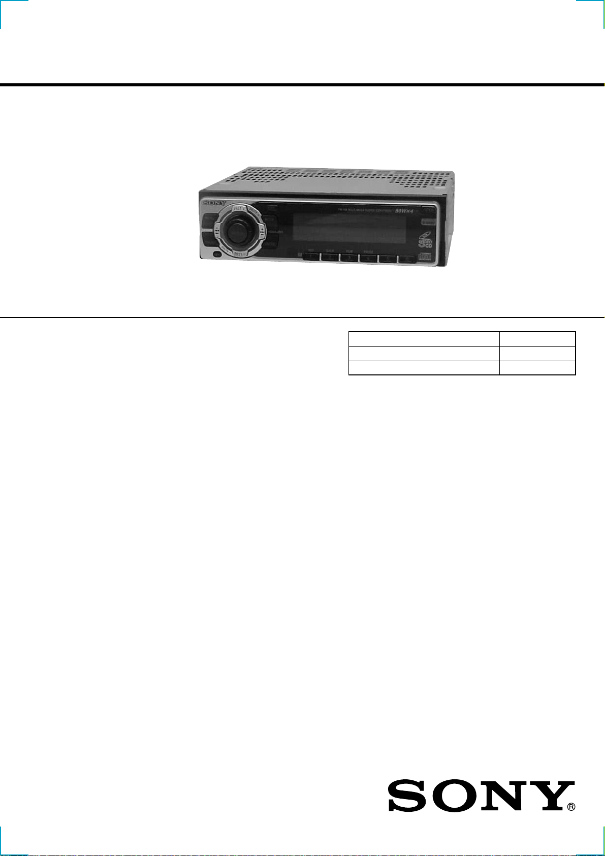
CDX-V7800X
SERVICE MANUAL
Ver 1.2 2001.07
• The tuner and CD sections have no adjustments.
SPECIFICATIONS
E Model
Tourist Model
Model Name Using Similar Mechanism NEW
CD Drive Mechanism Type MG-383K-121//K
Optical Pick-up Name KSS-720A
CD player section
System Compact disc digital audio
system
Signal-to-noise ratio 90 dB
Frequency response 10 – 20,000 Hz
Wow and flutter Below measurable limit
Signal format system PAL/NTSC
Tuner section
FM
Tuning range FM tuning interval:
50 kHz/200 kHz
switchable
87.5 – 108 MHz
(at 50 kHz step)
87.5 – 107.9 MHz
(at 200 kHz step)
Aerial terminal External aerial connector
Intermediate frequency 10.7 MHz/450 kHz
Usable sensitivity 9 dBf
Selectivity 75 dB at 400 kHz
Signal-to-noise ratio 65 dB (stereo),
68 dB (mono)
Harmonic distortion at 1 kHz
0.7% (stereo),
0.4% (mono)
Separation 35 dB at 1 kHz
Frequency response 30 – 15,000 Hz
AM
Tuning range AM tuning interval:
9 kHz/10 kHz switchable
531 – 1,602 kHz
(at 9 kHz step)
530 – 1,710 kHz
(at 10 kHz step)
Aerial terminal External aerial connector
Intermediate frequency 10.7 MHz/450 kHz
Sensitivity 30 µV
Power amplifier section
Outputs Speaker outputs
(sure seal connectors)
Speaker impedance 4 – 8 ohms
Maximum power output 50 W × 4 (at 4 ohms)
General
Outputs Audio outputs
Video output
Power aerial relay control
lead
Power amplifier control
lead
Input Telephone ATT control
lead
Parking break control lead
Tone controls Bass ±9 dB at 100 Hz
Treble ±9 dB at 10 kHz
Power requirements 12 V DC car battery
(negative earth)
Dimensions Approx. 178 × 50 × 183 mm
(w/h/d)
Mounting dimensions Approx. 182 × 53 × 162 mm
(w/h/d)
Mass Approx. 1.2 kg
Supplied accessories Parts for installation and
connections (1 set)
Front panel case (1)
Card remote commander RM-X200
Design and specifications are subject to change without
notice.
FM/AM MULTI MEDIA PLAYER
9-870-201-13
2001G0400-1
© 2001.7
Sony Corporation
e Vehicle Company
Shinagawa Tec Service Manual Production Group
1

SERVICE NOTES
TABLE OF CONTENTS
NOTES ON HANDLING THE OPTICAL PICK-UP BLOCK
OR BASE UNIT
The laser diode in the optical pick-up block may suffer electrostatic
breakdown because of the potential difference generated by the
charged electrostatic load, etc. on clothing and the human body.
During repair, pay attention to electrostatic breakdown and also use
the procedure in the printed matter which is included in the repair
parts.
The flexible board is easily damaged and should be handled with
care.
NOTES ON LASER DIODE EMISSION CHECK
The laser beam on this model is concentrated so as to be focused on
the disc reflective surface by the objective lens in the optical pickup block. Therefore, when checking the laser diode emission, observe from more than 30 cm away from the objective lens.
Notes on Chip Component Replacement
• Never reuse a disconnected chip component.
• Notice that the minus side of a tantalum capacitor may be dam-
aged by heat.
1. GENERAL
About Discs .............................................................................3
Location of Controls................................................................ 3
Getting Started......................................................................... 3
CD ........................................................................................... 4
Video CD/Super VCD ............................................................. 5
Radio ....................................................................................... 6
Other Functions .......................................................................6
MP3 File Instruction................................................................ 7
Connections ............................................................................. 9
2. DISASSEMBLY
2-1. Sub Panel (CD) Assy......................................................... 10
2-2. CD Mechanism Block ....................................................... 10
2-3. Main Board ....................................................................... 11
2-4. Heat Sink ........................................................................... 11
2-5. Chassis (T) Sub Assy ........................................................12
2-6. Lever Section..................................................................... 12
2-7. Servo Board....................................................................... 13
2-8. Shaft Roller Assy .............................................................. 13
2-9. Floating Block Assy .......................................................... 14
2-10. Optical Pick-up Block ....................................................... 14
3. DIAGRAMS
3-1. IC Pin Descriptions ...........................................................15
3-2. Block Diagram –Tuner Section–....................................... 23
3-3. Block Diagram –CD Section–........................................... 24
3-4. Block Diagram –MPEG Section– .....................................25
3-5. Block Diagram –Display Section–.................................... 26
3-6. Circuit Boards Location ....................................................26
3-7. Printed Wiring Board –CD Mechanism Section– .............28
3-8. Schematic Diagram –CD Mechanism Section (1/3)– .......30
3-9. Schematic Diagram –CD Mechanism Section (2/3)– .......31
3-10. Schematic Diagram –CD Mechanism Section (3/3)– .......32
3-11. Schematic Diagram –Main Section (1/2)– ........................ 33
3-12. Schematic Diagram –Main Section (2/2)– ........................ 34
3-13. Printed Wiring Board –Main Section– .............................. 35
3-14. Schematic Diagram –Relay Section–................................ 36
3-15. Printed Wiring Board –Relay Section– ............................. 37
3-16. Printed Wiring Board –Display Section– .......................... 38
3-17. Schematic Diagram –Display Section–............................. 39
SAFETY-RELATED COMPONENT WARNING!!
COMPONENTS IDENTIFIED BY MARK 0 OR DOTTED LINE
WITH MARK 0 ON THE SCHEMATIC DIAGRAMS AND IN
THE PARTS LIST ARE CRITICAL TO SAFE OPERATION.
REPLACE THESE COMPONENTS WITH SONY PARTS WHOSE
P ART NUMBERS APPEAR AS SHOWN IN THIS MANU AL OR
IN SUPPLEMENTS PUBLISHED BY SONY.
2
4. EXPLODED VIEWS
4-1. Chassis Section ................................................................. 42
4-2. Front Panel Section ...........................................................43
4-3. CD Mechanism Section (1) ............................................... 44
4-4. CD Mechanism Section (2) ............................................... 45
4-5. CD Mechanism Section (3) ............................................... 46
5. ELECTRICAL PARTS LIST ........................................47
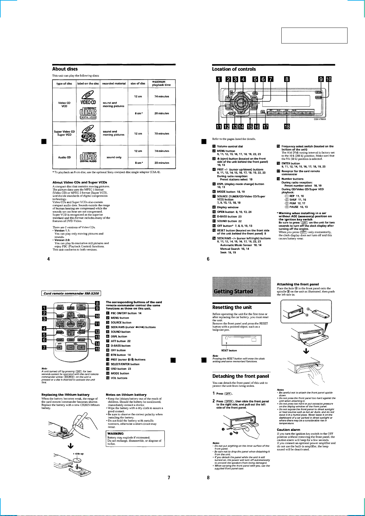
SECTION 1
GENERAL
This section extracted
from instruction manual.
3
456
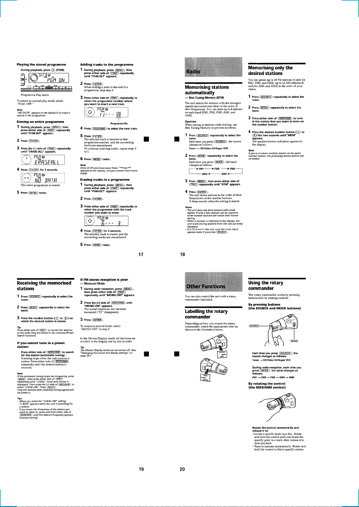
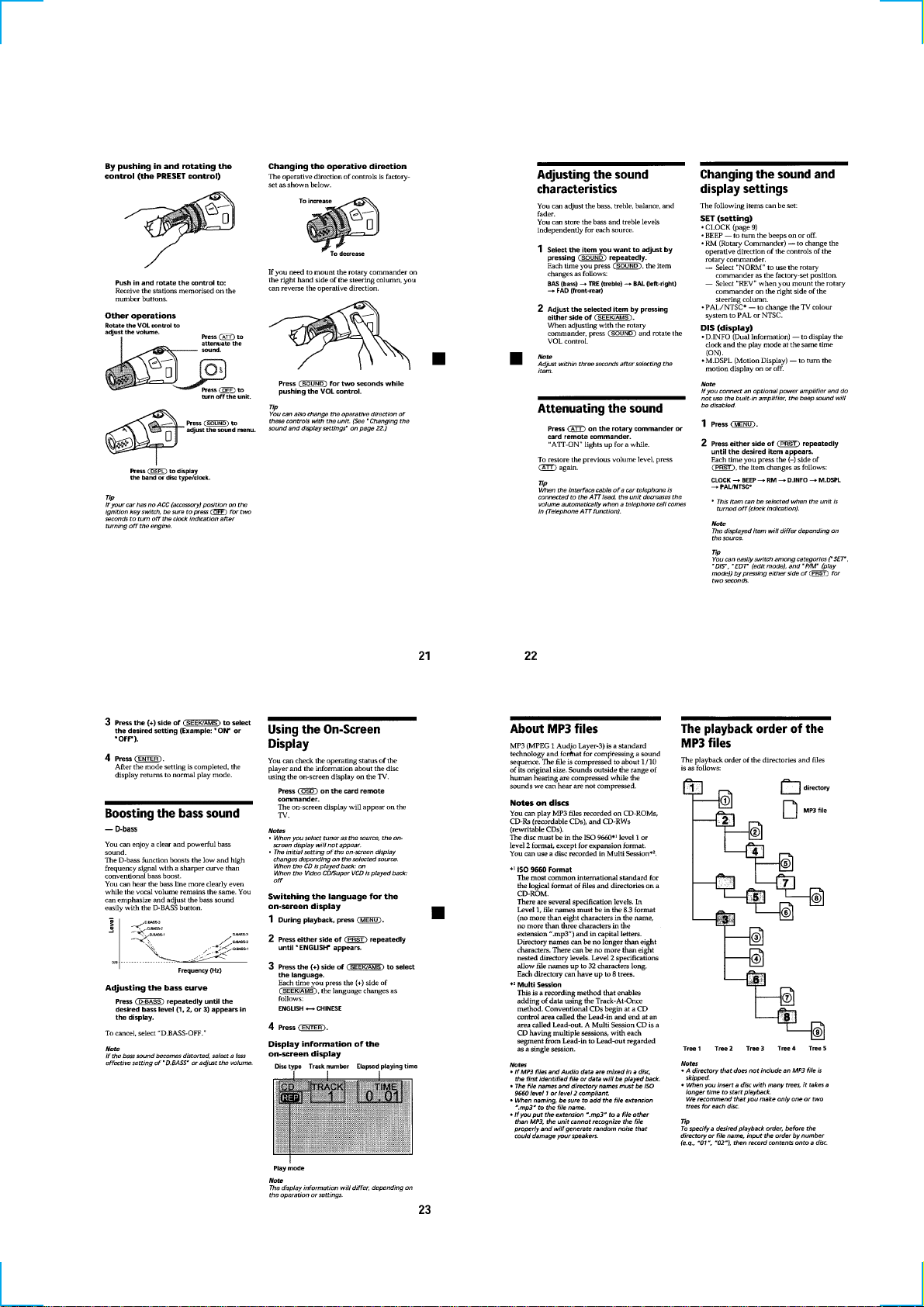
MP3 FILE INSTRUCTION
7
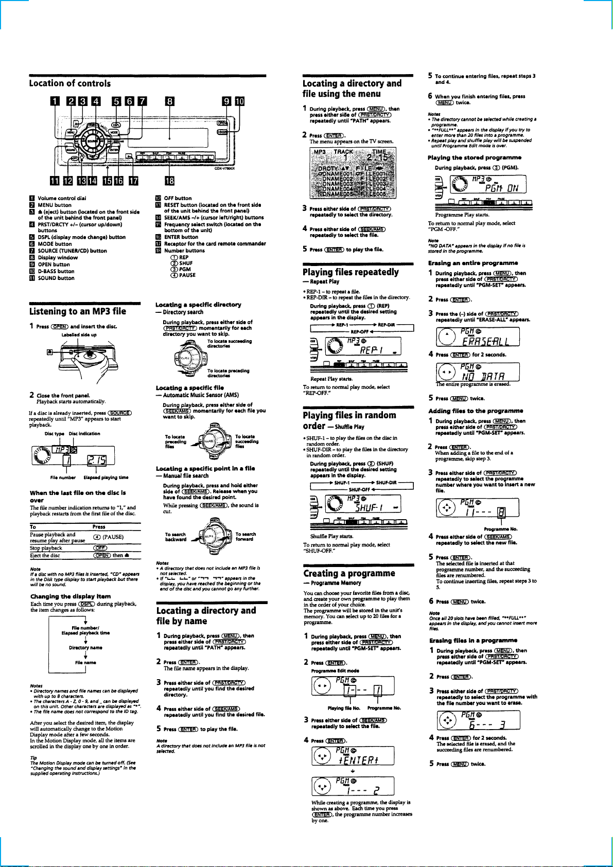
8
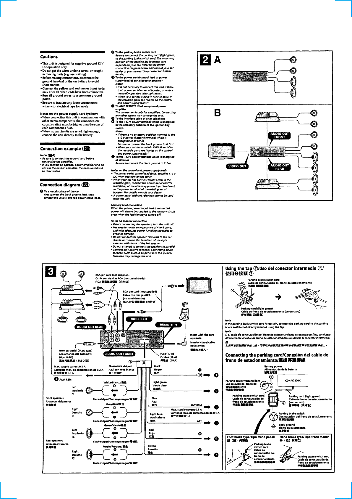
CONNECTIONS
9
6
SECTION 2
DISASSEMBLY
Note : Follow the disassembly procedure in the numerical order given.
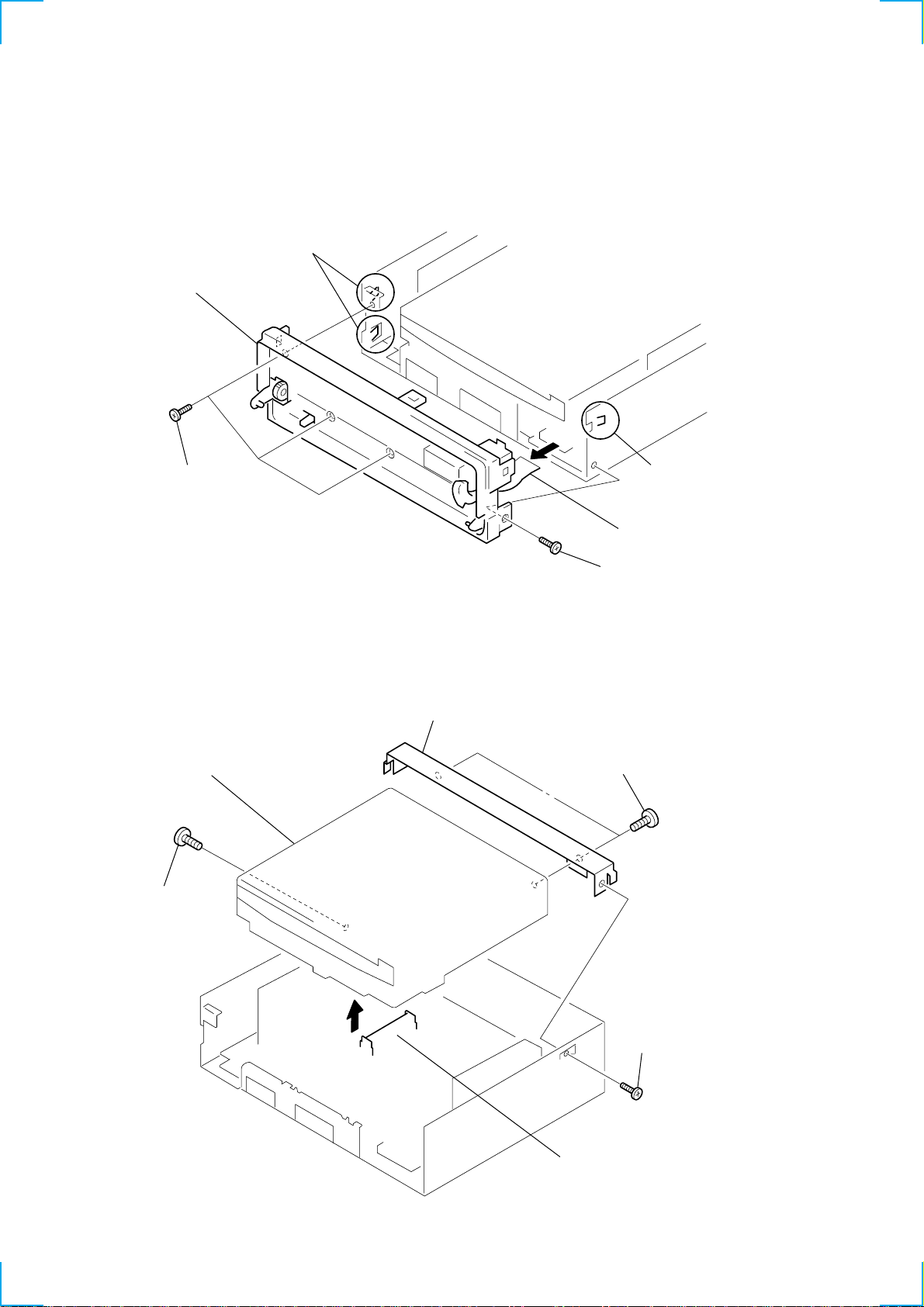
2-1. SUB PANEL (CD) ASSY
4 two claws
6 sub panel (CD) assy
2 PTT 2.6x6
2-2. CD MECHANISM BLOCK
5 CD mechanism block
2 PTT 2.6x6
3 claw
5 CNP800
1 PTT 2.6x6
7 bracket (CD)
6 PTT 2.6x6
10
3
4 CN701
1 PTT 2.6x
7 heat sink
1 PTT 2.6x8
2 PTT 2.6x8
4 PTT 2.6x8
5 PTT 2.6x8
3 PTT 2.6x12
6 PTT 2.6x8
8
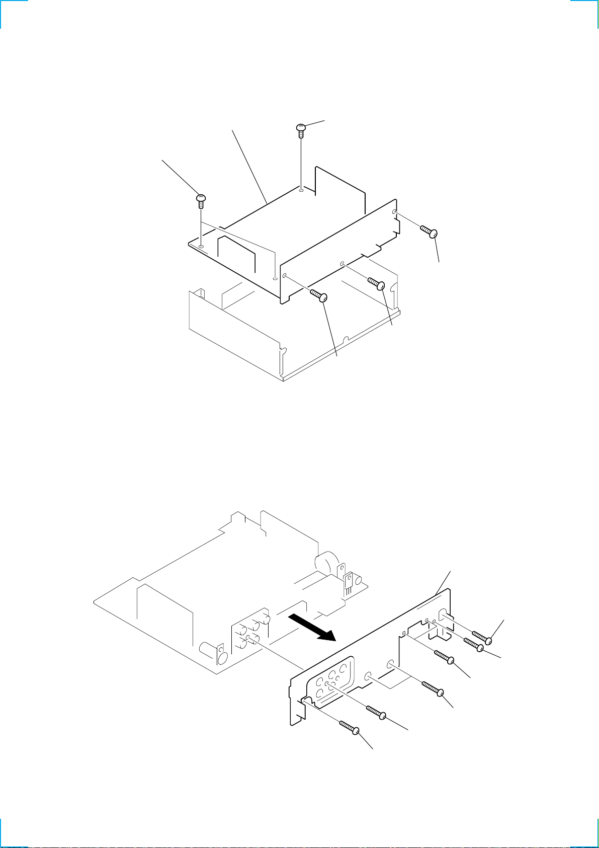
2-3. MAIN BOARD
5 screws (BTT)
6 MAIN board
4 screws (BTT)
3 PTT 2.6x
2 PTT 2.6x8
1 PTT 2.6x8
2-4. HEAT SINK
11
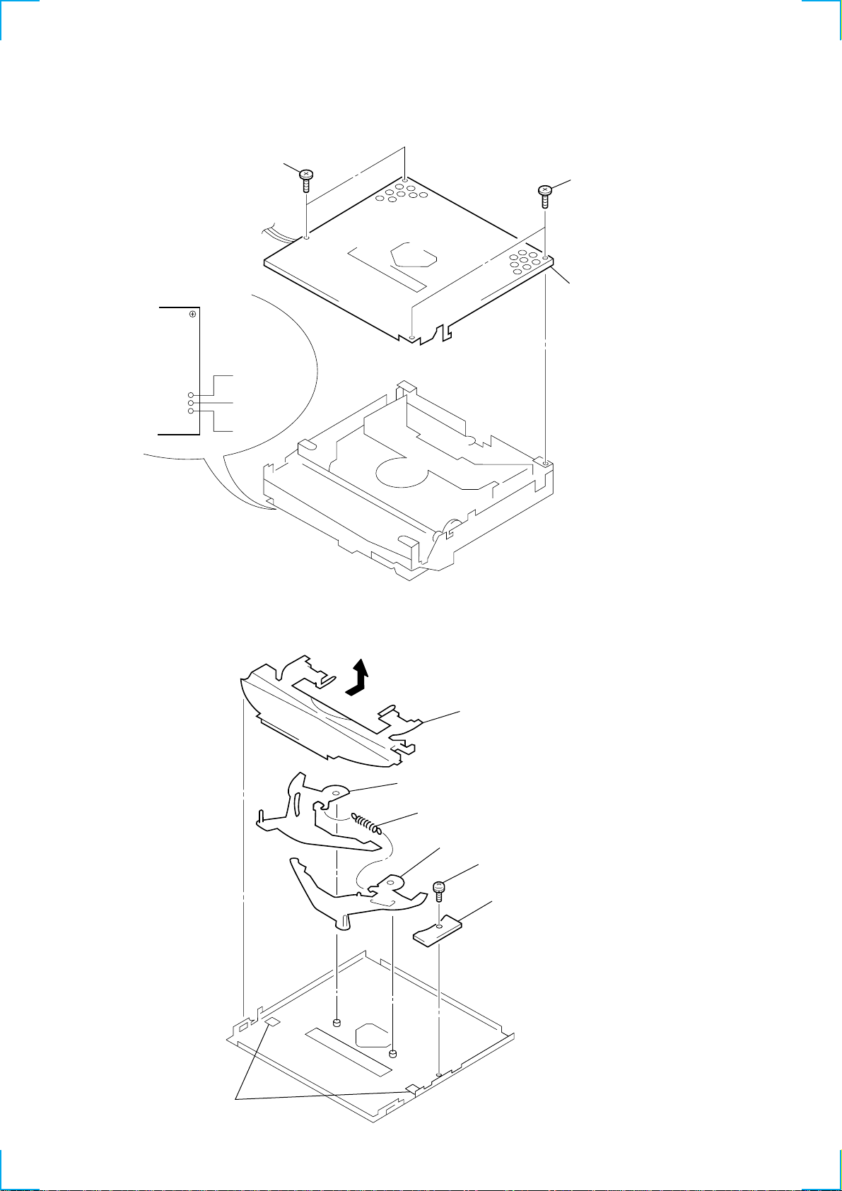
2-5. CHASSIS (T) SUB ASSY
2 P 2x3
3 P 2x3
1 Unsolder the
lead wires.
2-6. LEVER SECTION
4 chassis (T) sub assy
black
red
white
4
claws
6
lever (R)
3
tension spring (LR)
7
lever (L)
5
guide (disc)
1
special screw
2
DISC IN SW board
12
r
w
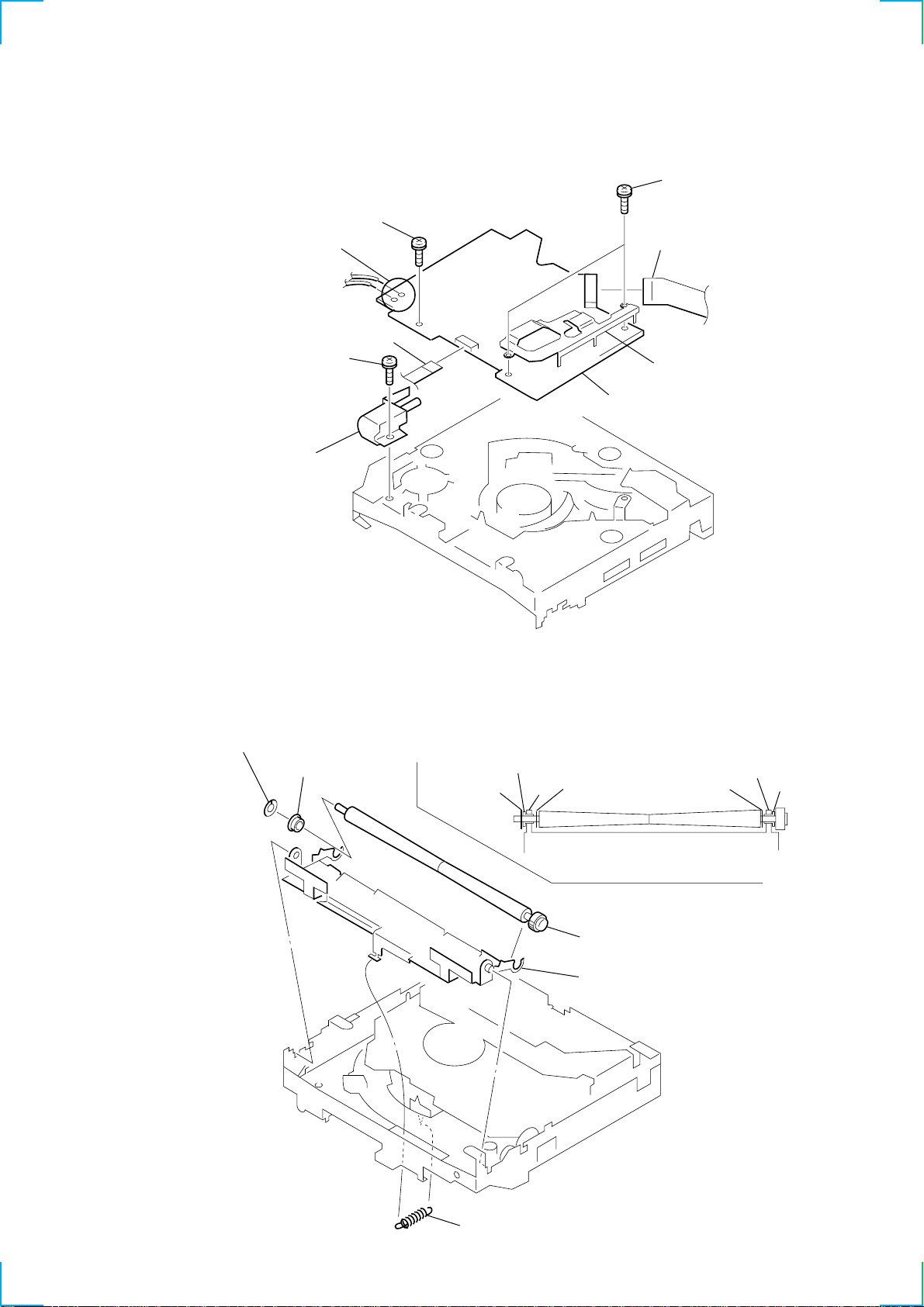
2-7. SERVO BOARD
3 Removal the solders.
6 Special screw
1 CN517
4 P 2x3
5 LO motor sub assy
(M903)
7 Special scre
2 CN518
8 heat sink (CD)
9 SERVO board
2-8. SHAFT ROLLER ASSY
3 retaing ring (RA)
4 shaft retainer
shaft retainer
retaing ring (RA)
washer
arm
washer
arm
shaft retaine
Fig. 1
5 shaft roller assy
2 arm (roller)
1 tension spring (RA)
13
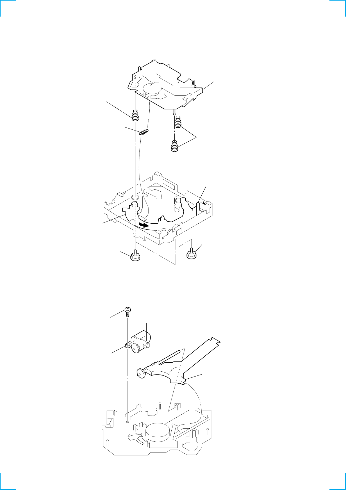
2-9. FLOATING BLOCK ASSY
7 compression spring (FL)
1 tension spring (KF1)
6 floating block assy
8 compression spring (FL)
4 Fit lever (D) in the
direction of the arrow.
5 Turn loading ring in the
direction of the arrow.
3 damper (T)
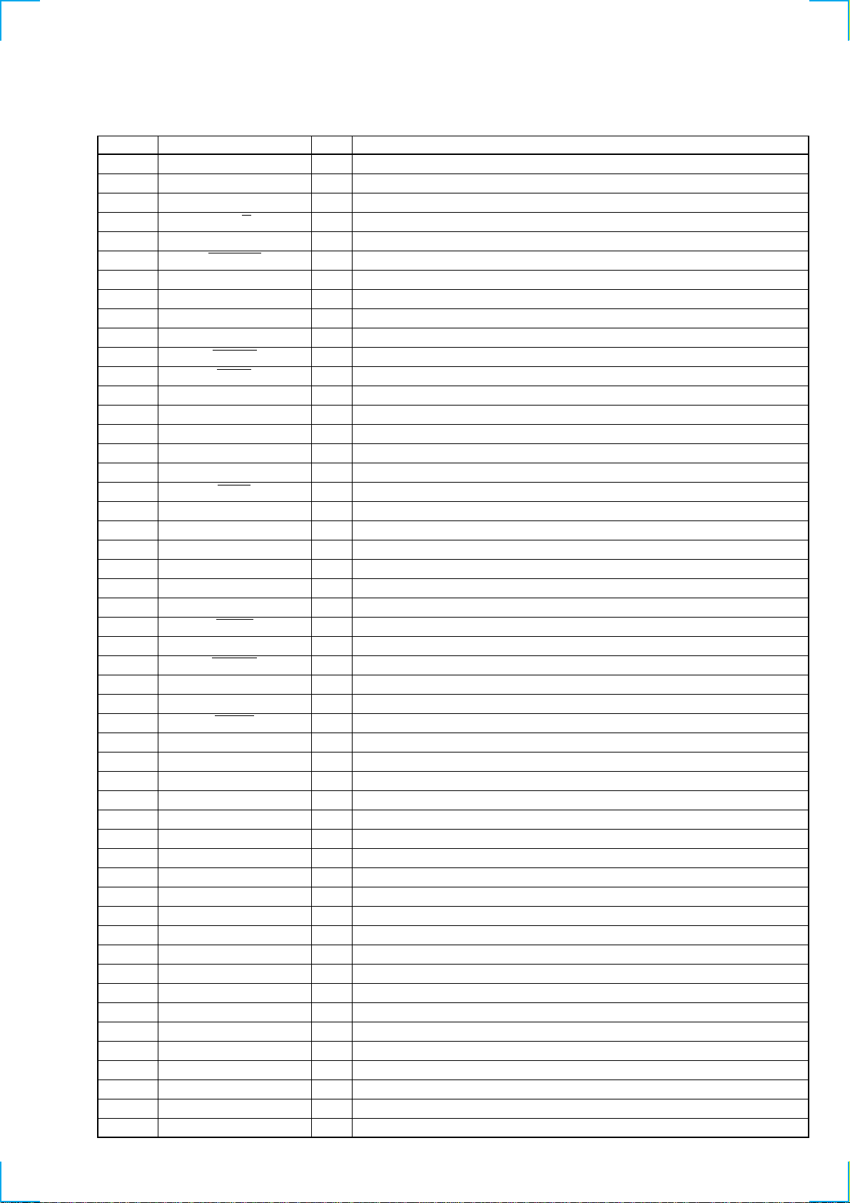
2-10. OPTICAL PICK-UP BLOCK
1 P 2x3
2 sled motor assy
(M902)
2 damper (T)
3 optical pick-up block
14
SECTION 3
DIAGRAMS
3-1. IC PIN DESCRIPTIONS
• IC513 CXP81960M-659R (CD SYSTEM CONTROL)
Pin No. Pin Name I/O Pin Description
1 A MUTE O Audio mute control output
2 N.C — Not used. (Open)
3 CD ON O CD servo power supply control output
4 RW/R O RF amplifier gain control output (H: CD-RW, L: CD-R/CD-DA)
5 SLD MINUS O Sled motor control output
6 SELF SW I Disc self store switch input
7 E/(U) I Destination setting input (Fixed at H in this set)
8 PH1 I Photo coupler input 1 (Not used in this set)
9 SDA I/O I2C interface data input/output for video encoder IC.
10 SCL O I2C interface clock output to video encoder IC.
11 H WAIT I Wait input from MPEG decoder (Host) IC.
12 H INT I Interruption input from MPEG decoder IC.
13 – 20 HDATA7 – 0 I/O Host data 7 – 0 input for MPEG decoder IC.
21 EMPH O O D/A converter emphasis control output to DSP IC.
22 CD DATA O Data output to CD servo IC.
23 CD XTAL O System latch output to CD servo IC.
24 CD CKO O Clock output to CD servo IC.
25 D SW I Disc switch input
26 N.C — Not used. (Fixed at H in this set)
27 LIMIT SW I Sled limit switch input
28 SUBQ I CD sub-Q serial data input from DSP IC.
29 N.C — Not used. (Open)
30 SQCK O Sub-Q clock output to DSP IC.
31 N.C — Not used. (Open)
32 MSRQ O Serial request output of master microcomputer.
33 N.C — Not used. (Open)
34 CD RST O CD reset output
35, 36 N.C — Not used. (Open)
37 MP I Connect to VSS.
38 RESET I Slave microcomputer hard reset input
39 VSS — Ground
40 XTAL O Crystal oscillation output (12 MHz)
41 EXTAL I Crystal oscillation input (12 MHz)
42 N.C — Not used. (Fixed at H in this set)
43 TEXT IN I Not used. (Connect to SUBQ)
44 N.C — Not used. (Open)
45 TEXT CLK O Not used. (Connect to SQCK)
46 PH2 I Photo coupler input 2 (Not used in this set)
47 – 49 N.C — Not used. (Open)
50 AVSS — Analog ground
51 AVREF — Analog power supply reference input
52 AVDD — Analog power supply pin
53 GFS/MNT2 SEL I GFS/MNT2 select input of DSP IC. (Fixed at H in this set)
54 N.C — Not used. (Fixed at H in this set)
55 FOK I Focus OK input from DSP IC.
56 GFS I Guard frame synchro input from DSP IC.
57, 58 N.C — Not used. (Fixed at L in this set)
59 TEMP H I Not used. (Open)
60 TEMP L I Not used. (Open)
61 LOCK I Lock input from DSP IC.
62 TEST MODE I Not used. (Fixed at H in this set)
15
Pin No. Pin Name I/O Pin Description
63 SENS I Sensitivity input from DSP IC.
64 IN SW I Disc in switch input
65, 66 N.C — Not used. (Fixed at H in this set)
67 MP3 I MP3 playback control input (H: not playback, L: playback)
68 PH3 I Photo coupler input 3 (Not used in this set)
69 SCLK O Serial clock output to DSP IC.
70 LM LOADING O Loading motor loading (CD tray close) output
71 TV RST O TV encoder IC reset output
72 N.C — Not used. (Open)
73 TE CANCEL O Tracking error offset cancel output of RF amplifier. (Not used in this set)
74 FE CANCEL O Focus error offset cancel output of RF amplifier. (Not used in this set)
75 BU IN I Back-up power supply input
76 SCOR I SCOR input from DSP IC.
77 MSO I Serial input from master microcomputer IC.
78 MSI O Serial output to master microcomputer IC.
79 MSC I Serial clock input from master microcomputer IC.
80 MCS I Chip select input from master microcomputer IC.
81 LM EJECT O Loading motor eject (CD tray open) output
82 DRV OE O Mute control output for driver IC.
83 MD2 O Check output for operation mode. (Not used in this set)
84 TEX I Not used. (Connect to VSS)
85 TX O not used. (Open)
86 VSS — Digital ground
87 VDD — Digital power supply pin
88 N.C — Not used. (Fixed at H in this set)
89 H R/W O Read/Write select output for MPEG decoder IC. (H: Read, L: Write)
90 H RD O Mode select output for MPEG decoder IC at read. (H: Multiflux, L: Individual)
91 – 93 HADDR2 – 0 O Host address 2 – 0 output for MPEG decoder IC.
94 H CS O Host chip select output for MPEG decoder IC.
95 N.C — Not used. (Open)
96 H RST O Host reset output
97 – 99 N.C — Not used. (Open)
100 CDM ON O CD mechanism deck loading motor power supply control output (8 V).
16
• IC514 CL8830-PE0 (MPEG DECODER)
Pin No. Pin Name I/O Pin Description
1 RESERVED I Fixed at L in this set.
2 – 4 HDATA0 – 2 I/O 8-bit bi-directional host data bus 0 – 2 input/output
5 VDD — Power supply pin (+3.3 V)
6 HDATA3 I/O 8-bit bi-directional host data bus 3 input/output
7 VSS — Ground
8 – 11 HDATA4 – 7 I/O 8-bit bi-directional host data bus 4 – 7 input/output
12 VDD2.5 — Power supply pin (+2.5 V)
13 RESET I Hardware reset input
14 VSS — Ground
15 WAIT O Host wait output
16 INT O Host interrupt output
17 VDD — Power supply pin (+3.3 V)
18 NC O Not used. (Open)
19 VSS — Ground
20 – 26 NC O Not used. (Open)
27 VDD — Power supply pin (+3.3 V)
28 NC O Not used. (Open)
29 VSS — Ground
30 – 35 NC O Not used. (Open)
36 VDD — Power supply pin (+3.3 V)
37 NC O Not used. (Open)
38 VSS — Ground
39 NC O Not used. (Open)
40 VDD2.5 — Power supply pin (+2.5 V)
41 NC O Not used. (Open)
42 VSS — Ground
43 – 46 NC O Not used. (Open)
47 VDD — Power supply pin (+3.3 V)
48 NC O Not used. (Open)
49 VSS — Ground
50, 51 NC O Not used. (Open)
52 RESERVED I Fixed at L in this set.
53, 54 MDATA15, 0 I/O Memory data 15 and 0 input/output
55 VDD — Power supply pin (+3.3 V)
56 MDATA14 I/O Memory data 14 input/output
57 VSS — Ground
58 – 60 MDATA1, 13, 2 I/O Memory data 1, 13 and 2 input/output
61 VDD — Power supply pin (+3.3 V)
62 MDATA12 I/O Memory data 12 input/output
63 VSS — Ground
64 MDATA3 O I/O Memory data 3 input/output
65 VDD2.5 — Power supply pin (+2.5 V)
66 MDATA11 I/O Memory data 11 input/output
67 VSS — Ground
68 MDATA4 I/O Memory data 4 input/output
69 VDD — Power supply pin (+3.3 V)
70 MDATA10 I/O Memory data 10 input/output
71 VSS — Ground
72 – 74 MDATA5, 9, 6 I/O Memory data 5, 9 and 6 input/output
75 VDD — Power supply pin (+3.3 V)
76 MDATA8 I/O Memory data 8 input/output
77 VSS — Ground
17
Pin No. Pin Name I/O Pin Description
78 MDATA7 I/O Memory data 7 input/output
79 LDQM O SDRAM LDQM output
80 UDQM O SDRAM UDQM output
81 VDD — Power supply pin (+3.3 V)
82 MWE O SDRAM write enable output
83 VSS — Ground
84 SD-CLK O SDRAM system clock output
85 SD-CAS O SDRAM column address output
86 SD-RAS O SDRAM row address output
87 VDD — Power supply pin (+3.3 V)
88 SD-CS1 O SDRAM bank select 1 output (Not used in this set)
89 VSS — Ground
90 SD-CS0 O SDRAM bank select 0 output
91 VDD2.5 — Power supply pin (+2.5 V)
92 NC O Not used. (Open)
93 VSS — Ground
94 NC O Not used. (Open)
95 VDD — Power supply pin (+3.3 V)
96 MADDR9 O Memory address 9 output
97 VSS — Ground
98 – 100 MADDR11, 8, 10 O Memory address 11, 8 and 10 output
101 VDD — Power supply pin (+3.3 V)
102 MADDR7 O Memory address 7 output
103 VSS — Ground
104 – 106 MADDR0, 6, 1 O Memory address 0, 6 and 1 output
107 VDD — Power supply pin (+3.3 V)
108 MADDR5 O Memory address 5 output
109 VSS — Ground
110 – 112 MADDR2, 4, 3 O Memory address 2, 4 and 3 output
113 VDD — Power supply pin (+3.3 V)
114 MADDR12 O Memory address 12 output
115 VSS — Ground
116 MADDR13 O Memory address 13 output
117 VDD2.5 — Power supply pin (+2.5 V)
118 MADDR14 O Memory address 14 output
119 VSS — Ground
120 – 122 MADDR15 – 17 O Memory address 15 – 17 output
123 VDD — Power supply pin (+3.3 V)
124 MADDR18 O Memory address 18 output
125 VSS — Ground
126, 127 MADDR19, 20 O Memory address 19 and 20 output
128 ROM-CS O ROM chip select output
129 RESERVED I Fixed at L in this set.
130 NC O Not used. (Open)
131, 132 GND — Ground
133 RESERVED I Fixed at L in this set.
134 VDD — Power supply pin (+3.3 V)
135 RESERVED I Fixed at L in this set.
136 VSS — Ground
137 – 141 RESERVED I Fixed at L in this set.
142, 143 VDATA0, 1 O Video data bus 0 and 1 output
144 VDD2.5 — Power supply pin (+2.5 V)
145 VDATA2 O Video data bus 2 output
18
 Loading...