

Page 1
CDX-V2800
SERVICE MANUAL
Ver. 1.0 2005. 11
• The tuner and CD sections have no adjustments.
SPECIFICATIONS
E Model
Model Name Using Similar Mechanism NEW
CD Drive Mechanism Type MG-611MM-186//Q
Optical Pick-up Name KSS1000E
CD player section
Signal-to-noise ratio 90 dB
Frequency response 10 – 20,000 Hz
Wow and flutter Below measurable limit
Signal format system PAL/NTSC
Tuner section
FM
Tuning range FM tuning interval:
50 kHz/200 kHz
switchable
87.5 – 108.0 MHz
(at 50 kHz step)
87.5 – 107.9 MHz
(at 200 kHz step)
Aerial terminal External aerial connector
Intermediate frequency 10.7 MHz/450 kHz
Usable sensitivity 9 dBf
Selectivity 75 dB at 400 kHz
Signal-to-noise ratio 67 dB (stereo),
69 dB (mono)
Harmonic distortion at 1 kHz
0.5% (stereo),
0.3% (mono)
Separation 35 dB at 1 kHz
Frequency response 30 – 15,000 Hz
AM
Tuning range AM tuning interval:
9 kHz/10 kHz switchable
531 – 1,602 kHz
(at 9 kHz step)
530 – 1,710 kHz
(at 10 kHz step)
Aerial terminal External aerial connector
Intermediate frequency 10.7 MHz/450 kHz
Sensitivity 30 µV
Power amplifier section
Outputs Speaker outputs
(sure seal connectors)
Speaker impedance 4 – 8 ohms
Maximum power output 52 W × 4 (at 4 ohms)
General
Outputs Audio output terminals (rear/sub switchable)
Video output terminal
Power aerial relay control terminal
Power amplifier control terminal
Inputs AUX IN terminal
Parking brake control terminal
Aerial input terminal
Tone controls Low:
±10 dB at 60 Hz (XPLOD)
Mid:
±10 dB at 1 kHz (XPLOD)
High:
±10 dB at 10 kHz (XPLOD)
Power requirements 12 V DC car battery
(negative earth)
Dimensions Approx. 178 × 50 × 178 mm (w/h/d)
Mounting dimensions Approx. 182 × 53 × 161 mm (w/h/d)
Mass Approx. 1.2 kg
Supplied accessories Parts for installation and connections (1 set)
Front panel case (1)
Card remote commander RM-X159
MPEG Layer-3 audio coding technology and
patents licenced from Fraunhofer IIS and Thomson.
Design and specifications are subject to change without
notice.
9-879-928-01
2005K04-1
© 2005. 11
FM/AM MULTI MEDIA PLAYER
Sony Corporation
eVehicle Division
Published by Sony Engineering Corporation
1
Page 2
eclubthai eclubthai eclubthai eclubthai eclubthai
eclubthai eclubthai eclubthai eclubthai eclubthai
eclubthai eclubthai eclubthai eclubthai eclubthai
eclubthai eclubthai eclubthai eclubthai eclubthai
eclubthai eclubthai eclubthai eclubthai eclubthai
eclubthai eclubthai eclubthai eclubthai eclubthai
eclubthai eclubthai eclubthai eclubthai eclubthai
eclubthai eclubthai eclubthai eclubthai eclubthai
eclubthai eclubthai eclubthai eclubthai eclubthai
eclubthai eclubthai eclubthai eclubthai eclubthai
SECTION 3
DIAGRAMS
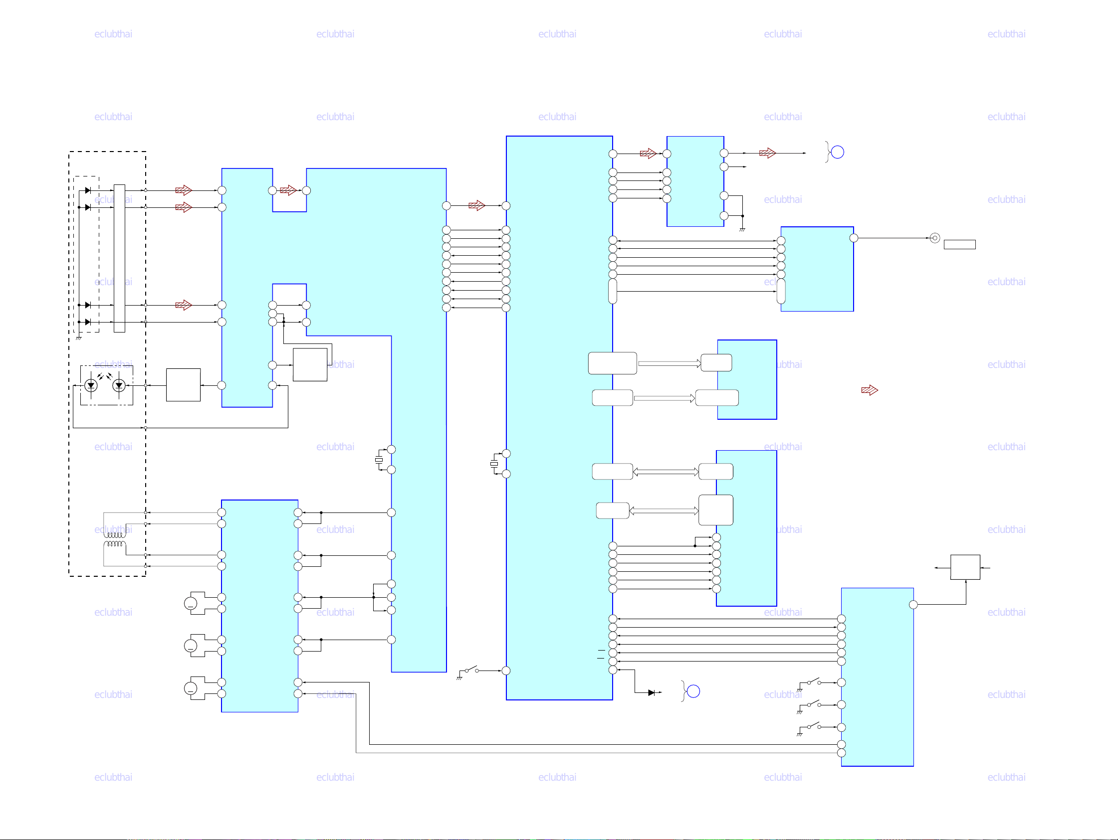
3-1. BLOCK DIAGRAM — CD SECTION —
CDX-V2800
2
1
3
14
12
DIGITAL
MODULATOR
DIN
LRCK
BCKIN
SCKI
DEEMP
IC700
LOUT
ROUT
MUTE
FORMAT
45•25–18•
8–1•48•17
29•31•33•35•
38•30•40•42•44
9
6
10
13
16M SDRAM
A18
IC200
A0
I
DQ0
DQ7
I
R-CH
28
29
15
14
9
17
I
24
VIDEO SIGNAL
PROCESSOR
VSYNC
HSYNC
CLK
MODEB
SLEEP
P0
I
P7
CD-L
IC400
MAIN
A
SECTION
(Page 14)
32
CVBS/Y
• R-ch is omitted due to same as L-ch.
• Siganal Path
: CD PLAY
PJ401 (1/2)
VIDEO OUT
RF AMP,
DIGITAL SERVO
DETECTOR
PD1
PD2
PD1
PD2
I-V AMP
2
BD
3
52
EQ0
AC
RFI
51
E
F
LASER DIODE
PD LD
E
F
LD
AUTOMATIC
POWER
CONTROL
Q501
5
6
13
FEO
E
F
LD
TZCRFM
TEO
LON
9
46
48
24
12
PD
FEN
8
TEN
49
LASER ON
CONTROL
SWITCH
Q502
IC500
DOUTA
LRCK
WFCK
DCK
EFLAG
SUBSYQ
BUSY
RESETX
R/W
DIN/OUT
MCK
35
36
34
37
38
31
30
29
28
27
26
DIGITAL SIGNAL PROCESSOR
CD DATA
96
CD LRCK
97
BATTLOW
50
CD BCLK
98
CD XCK
102
SUBSYQ
81
BUSY
80
XRESET
82
R/W
83
DI/DO
84
MCK
85
IC100
ROMA0
I
ROMA18
ROMD0
I
ROMD7
CLK27 OUT
77
AU DATA
78
AU LRCK
79
AU BCK
76
AU XCK
103
DEEMP
56
VSYNC
55
HSYNC
69
70
PLA NTSC
54
V RST
64
YC0
I
57
YC7
29–32•34•38•40•42
•41•39•33•35•44•
43•45–49
27•25•23•21•22
•24•26•28
I
ROMA0-ROMA18
ROMD0-ROMD7
MONOUT
16M SDRAM
OPTICAL
PICK-UP BLOCK
2-AXIS DEVICE
(FOCUS)
(TRACKING)
FCS+
FCS–
TRK+
TRK–
M902
(SLED)
M901
(SPINDLE)
M903
(LOADING)
M
M
M
FOCUS/TRACKING COIL DRIVE,
SLED/SPINDLE/LOADING
MOTOR DRIVE
IC600
16
VO4(+)
15
VO4(–)
VO3(+)
17
VO3(–)
18
14
VO1(+)
13
VO1(–)
VO2(+)
12
VO2(–)
11
10
VOL+
9
VOL–
IN1(–)
OUT1
IN2(–)
OUT2
IN3(–)
OUT3
IN4(–)
OUT4
FWD
REV
3
4
6
7
23
22
26
25
1
28
X541
16.934MHz
42
43
20
22
17
18
19
21
XI
XO
SD OUT
CLV OUT
JUMP0
TDOUT
SDIN
FD OUT
X401
27MHz
SW4
(LIMIT)
65
CLKIN
DA0
17–20•16–12
66
CLKIO
LIMIT
92
DA10
DD0
DD15
I
•111•110
116–123•6–2
I
•126–124
DQMO
114
9 15
WE B
10 16
CAS B
11 17
RASO BT
112 19
BAO
127 35
RAMCLK
SI
91
SO
93
SCK
99
RESET B
88
SP
89
MP
113
MUTE
RAMA0-RAMA10
RAMD0-RAMD15
MUTE
D701
21–24•
27–32•20
2•3•5•6•8•
9•11•12•39•
40•42•43•45
•46•48•49
MAIN
B
SECTION
(Page 14)
IC300
A0
I
A10
DQ0
I
DQ15
14
LDOM
36
UDQM
WE
CAS
RAS
BA
CLK
SW1
(DOWN)
SW2
(SELF)
SW3
(DISC IN)
SYSTEM CONTROL
CD SO
1990
CD SI
18
CD SCK
20
CD XRST
98
SP
54
MP
90
CD DSW
95
CD SELFSW
55
CD INSW
92
CD LOAD
93
EJECT
94
IC801 (1/3)
BU+3.3V U COM+3.3V
CD ON
87
BU+3.3V
REG
Q701,703
CDX-V2800
13 13
Page 3
eclubthai eclubthai eclubthai eclubthai eclubthai
eclubthai eclubthai eclubthai eclubthai eclubthai
eclubthai eclubthai eclubthai eclubthai eclubthai
eclubthai eclubthai eclubthai eclubthai eclubthai
eclubthai eclubthai eclubthai eclubthai eclubthai
eclubthai eclubthai eclubthai eclubthai eclubthai
eclubthai eclubthai eclubthai eclubthai eclubthai
eclubthai eclubthai eclubthai eclubthai eclubthai
eclubthai eclubthai eclubthai eclubthai eclubthai
eclubthai eclubthai eclubthai eclubthai eclubthai
CDX-V2800
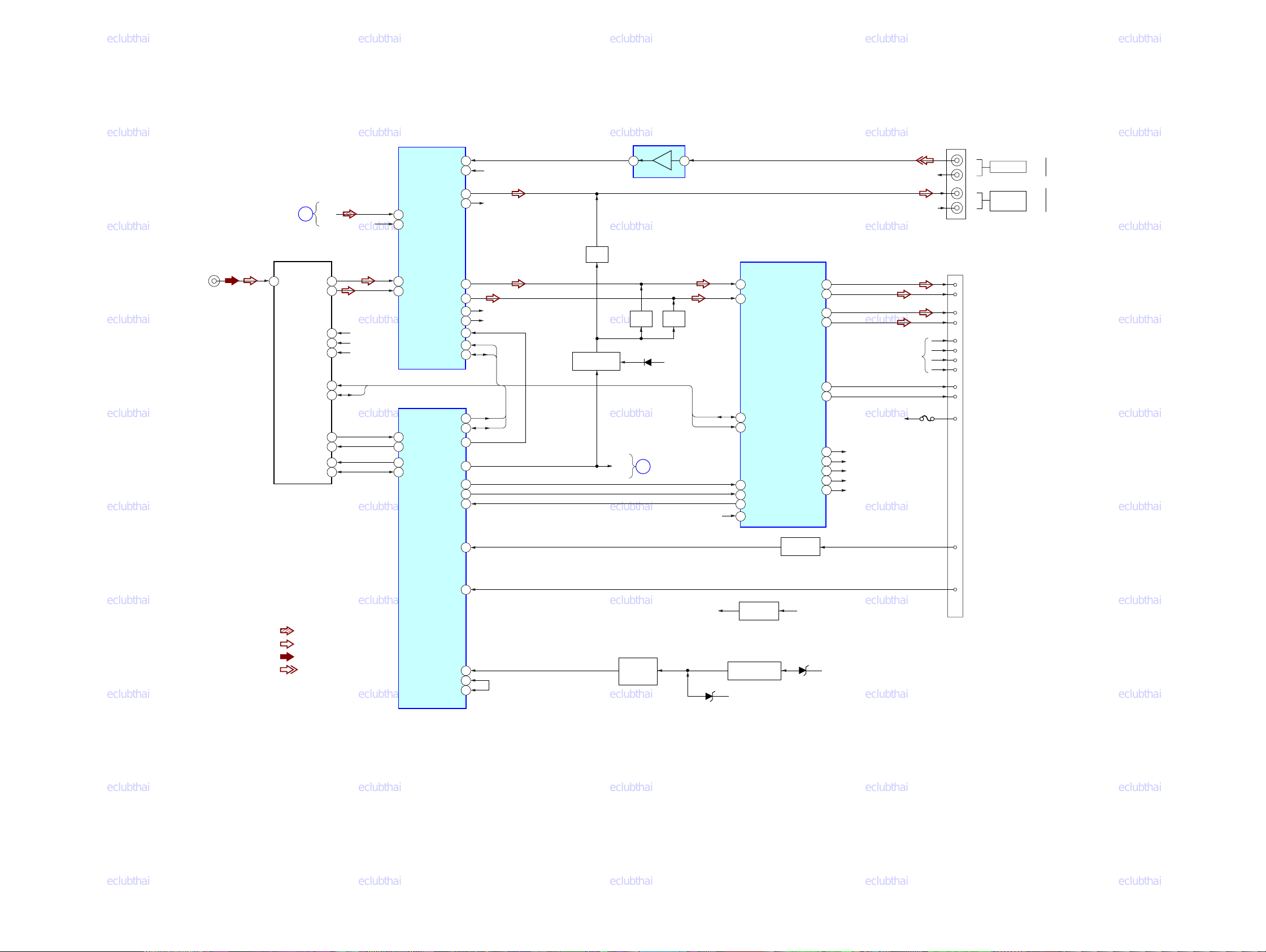
3-2. BLOCK DIAGRAM — MAIN SECTION —
CD
PJ601
(ANTENNA)
SECTION
(Page 13)
(TUNER UNIT)
1
ANT
TUX601
CD-L
A
L
R
R-CH
4
3
TU VDD
E2P VDD
TU-SCL
TU-SDA
15
13
14
TU+5V
U COM+3.3V
SCL
SDA
AU+8V
10
VCC
11
6
S-METER
7
TU MUTE
16
E2P SCL
17
E2P SDA
ELECTRONIC VOLUME
IC401
OUTS1
OUTS2
9
C2
8
C1
7
6
45
15
25
24
B2
B1
VSM
TU ATT
EEP SCK
EEP SIO
OUTF2
OUTR2
OUTF1
OUTR1
SYSTEM CONTROL
IC801 (2/3)
IIC SCK
IIC SIO
VOL ATT
LINE ATT
AP2
AP1
MUTE
SCL
SDA
BEEP
STB
DIAG
5
3
17
18
23
22
25
24
29
30
31
33
34
6
1
5
31
56
R-CH
R-CH
R-CH (FRONT)
R-CH (REAR)
SCL
SDA
SCL
SDA
MUTE
Q407
MUTE CONTROL
Q400,401
AUX AUDIO AMP
14 12
MUTE
Q405
D400
MUTE
B
IC402
MUTE
Q404
BATT
CD
SECTION
SDA
SCL
(Page 13)
BATT
12
11
2
4
16
22
25
35
POWER AMP
IN RR(FL)
IN RF(RL)
SDA
SCL
ACGND
STB
DIAG
VP
IC100
LF–
LR+
LR–
SW1
SW2
REG1
REG2
REG3
REG4
REG5
LF+
29
27
30
37
31
33
34
5
3
9
7
AU+8V
U-COM+3.3V
SERVO+3.3V
MECHA+6V
DISP+B
BATT
R-CH
R-CH
R-CH
F900
CNP801
1
9
2
10
4
12
3
11
5
6
16
L
R
L
R
FL+
F–
RL+
RL–
FR+
FR–
RR+
RR–
AMP-REM
ANT-REM
BATT
AUX IN
AUDIO OUT
REAR
PJ401 (2/2)
7
ACC
15
PARKING BRAKE
Q601
ACC CHECK
Q900
AU+8V
D912
BATT
ACC IN
64
PAK BK
67
• R-CH is omitted due to same as L-CH.
• Signal Path
: CD PLAY
: FM
: AM
: AUX
BU IN
UNI SI
UNI SO
TU+5V
53
58
59
BACK-UP
DETECT
Q906,907
D915
TU+5V REG
BATTERY CHECK
Q902
BATT
CDX-V2800
1414
Page 4
eclubthai eclubthai eclubthai eclubthai eclubthai
eclubthai eclubthai eclubthai eclubthai eclubthai
eclubthai eclubthai eclubthai eclubthai eclubthai
eclubthai eclubthai eclubthai eclubthai eclubthai
eclubthai eclubthai eclubthai eclubthai eclubthai
eclubthai eclubthai eclubthai eclubthai eclubthai
eclubthai eclubthai eclubthai eclubthai eclubthai
eclubthai eclubthai eclubthai eclubthai eclubthai
eclubthai eclubthai eclubthai eclubthai eclubthai
eclubthai eclubthai eclubthai eclubthai eclubthai
CDX-V2800
)
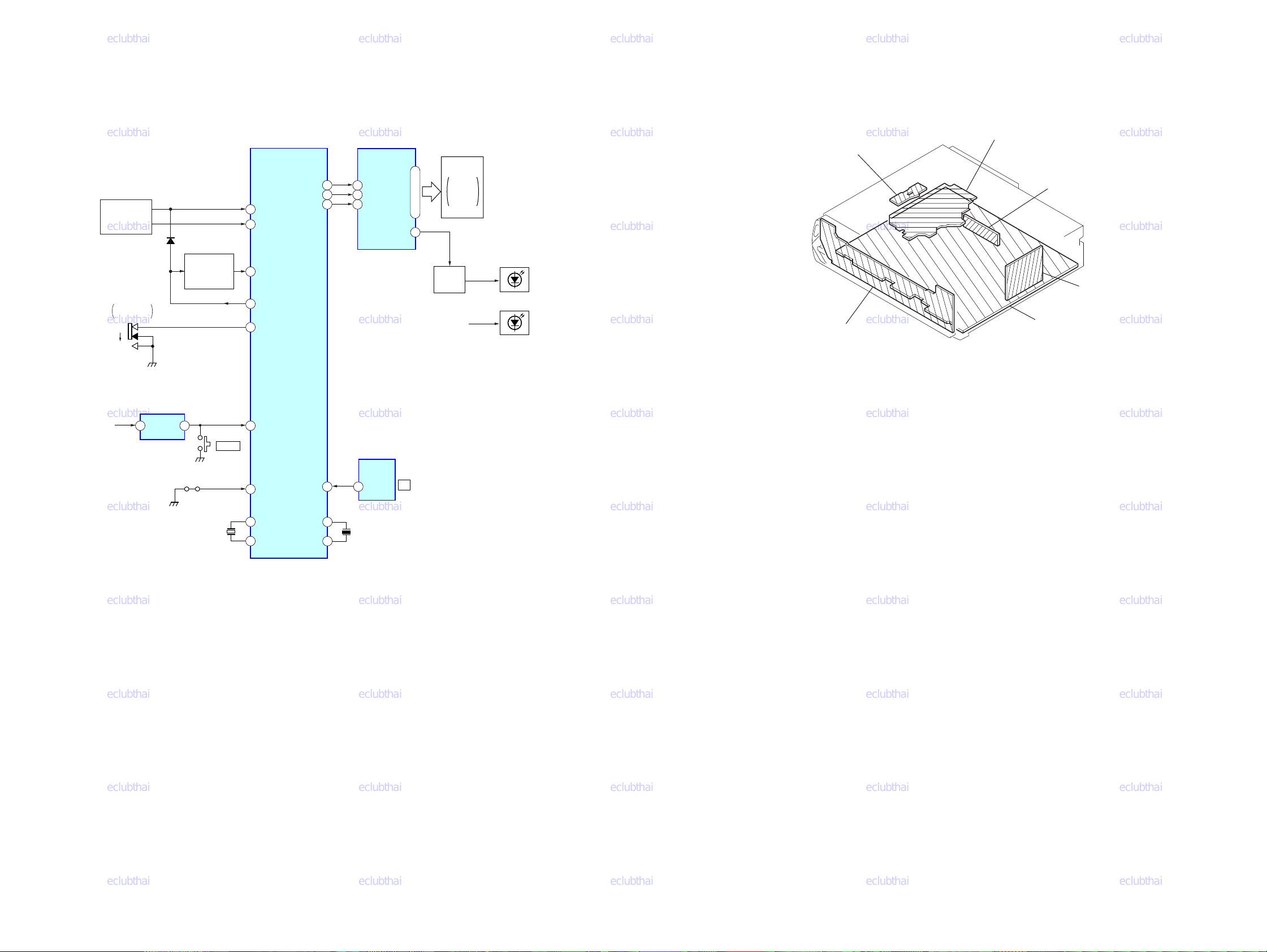
3-3. BLOCK DIAGRAM — DISPLAY SECTION —
KEY MATRIX
LSW901-911,
LSW913-921
D801
KEY
ACKNOWLEDGE
SWITCH
Q800
S800
FREQUENCY
SELECT
9K
10K
RESET
U COM+3.3V
IC802
OUT
2
IN
1
S802
RESET
SYSTEM CONTROL
IC801 (3/3)
KEYIN0
38
KEYIN1
39
KEY ACK
47
XKEY ON
75
DST SEL
46
RESET
77
LCD SO
LCD SCK
LCD CE
28
29
27
LCD DRIVER
IC901
64
DI
S48
CL
CLK
63
62
REMOTE CONTROL
SIGNAL RECEIVER
CE
CE
COM1
COM4
DIMMER
IC971
S1
|
4
I
55
|
1
LCD901
LIQUID
CRYSTAL
DISPLAY
LED
CONTROL
Q921
DISP+B
PANEL
LED931,932
LCD
()
BACK LIGHT
LED941,942,
LED951,952,
LSW901-911,
LSW913-921
3-4. CIRCUIT BOARDS LOCATION
SENSOR board
DISPLAY board
SERVO board
SPEAKER board
tuner unit
(TUX601
MAIN board
72
DOOR SW
SIRCS
65
OUT
2
IR
X801
32.768kHz
79
X0A
80
82
X0
X1
83
X800
18.432MHz
X1A
CDX-V2800
15 15
Page 5
eclubthai eclubthai eclubthai eclubthai eclubthai
eclubthai eclubthai eclubthai eclubthai eclubthai
eclubthai eclubthai eclubthai eclubthai eclubthai
eclubthai eclubthai eclubthai eclubthai eclubthai
eclubthai eclubthai eclubthai eclubthai eclubthai
eclubthai eclubthai eclubthai eclubthai eclubthai
eclubthai eclubthai eclubthai eclubthai eclubthai
eclubthai eclubthai eclubthai eclubthai eclubthai
eclubthai eclubthai eclubthai eclubthai eclubthai
eclubthai eclubthai eclubthai eclubthai eclubthai
CDX-V2800
THIS NOTE IS COMMON FOR PRINTED WIRING
BOARDS AND SCHEMATIC DIAGRAMS.
(In addition to this, the necessary note is printed
in each block.)
For schematic diagrams.
Note:
• All capacitors are in µF unless otherwise noted. (p: pF)
50 WV or less are not indicated except for electrolytics
and tantalums.
• All resistors are in Ω and
specified.
f
•
• C : panel designation.
Note: The components identified by mark 0 or dotted line
• A : B+ Line.
•Voltages and waveforms are dc with respect to ground
• CD mechanism section (1/2, 2/2)
no mark : CD PLAY
• Main (1/3), (2/3), (3/3) and Display sections
no mark : FM
: internal component.
with mark 0 are critical for safety.
Replace only with part number specified.
under no-signal (detuned) conditions.
(): AM
<>: CD PLAY
1
4
/
W or less unless otherwise
∗ : Impossible to measure
•Voltages are taken with a VOM (Input impedance 10 MΩ).
Voltage variations may be noted due to normal production tolerances.
•Waveforms are taken with a oscilloscope.
Voltage variations may be noted due to normal production tolerances.
• Circled numbers refer to waveforms.
• Signal path.
J : CD
F : FM
f : AM
L : AUX
For printed wiring boards.
Note:
• X : parts extracted from the component side.
• Y : parts extracted from the conductor side.
a
•
•
(The other layers' patterns are not indicated.)
Caution:
Pattern face side: Parts on the pattern face side seen from the
(Side B) pattern face are indicated.
Parts face side: Parts on the parts face side seen from the
(Side A) parts face are indicated.
: Through hole.
: Pattern from the side which enables seeing.
C
Q
CB
These are omitted.
EB
E
These are omitted.
C
BE
These are omitted.
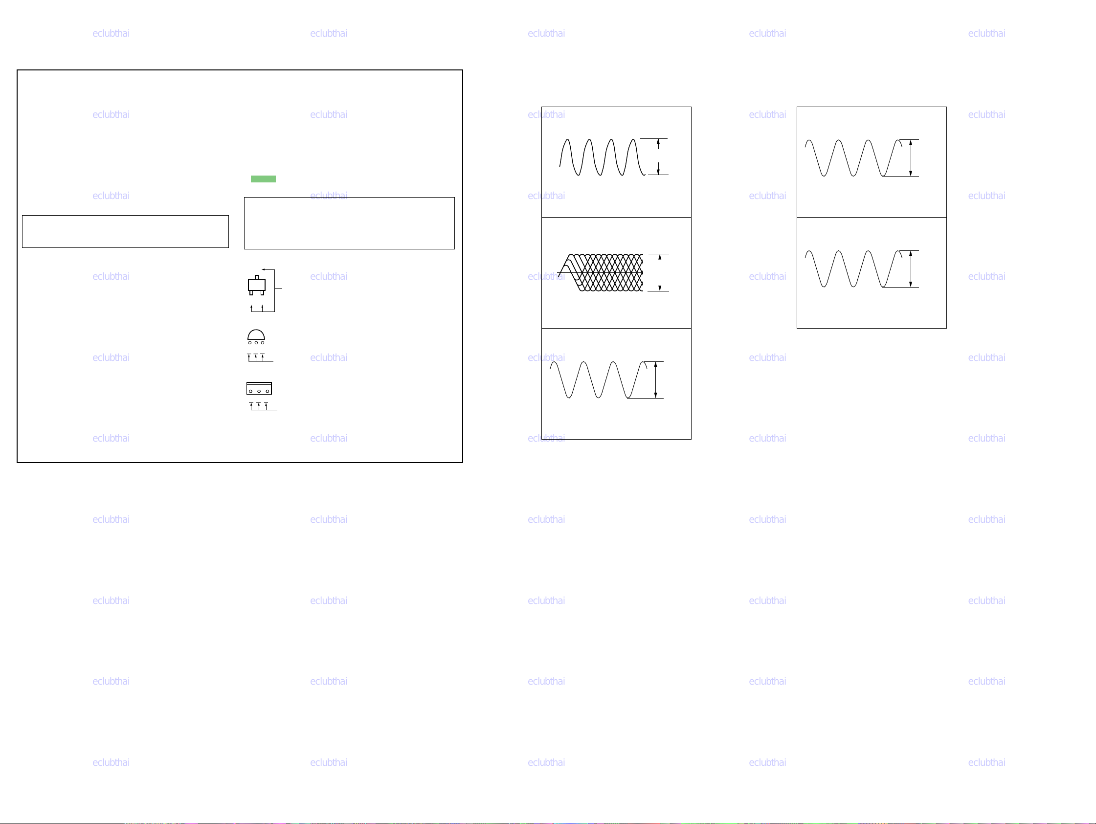
• Waveforms
— SERVO Board —
1
IC500 rd (XO)
16.9344 MHz
0.2 V/DIV, 0.2 µsec/DIV
2
IC500 ta (RFI)
0.5 V/DIV, 0.5
3
IC100 yg (CLKIN)
0.2 V/DIV, 0.2 µsec/DIV
µ
sec/DIV
27 MHz
(MODE: CD PLAY)
1.8 Vp-p
Approx.
0.8 Vp-p
1.5 Vp-p
— MAIN Board —
1
IC801 ul (X1A)
32.768 kHz
0.2 V/DIV, 20 µsec/DIV
2
IC801 id (X1)
18.432 MHz
0.5 V/DIV, 0.1
µ
sec/DIV
3.6 Vp-p
4.1 Vp-p
CDX-V2800
1616
Page 6

eclubthai eclubthai eclubthai eclubthai eclubthai
eclubthai eclubthai eclubthai eclubthai eclubthai
eclubthai eclubthai eclubthai eclubthai eclubthai
eclubthai eclubthai eclubthai eclubthai eclubthai
eclubthai eclubthai eclubthai eclubthai eclubthai
eclubthai eclubthai eclubthai eclubthai eclubthai
eclubthai eclubthai eclubthai eclubthai eclubthai
eclubthai eclubthai eclubthai eclubthai eclubthai
eclubthai eclubthai eclubthai eclubthai eclubthai
eclubthai eclubthai eclubthai eclubthai eclubthai
3-5. PRINTED WIRING BOARDS — CD MECHANISM SECTION — • Refer to page 15 for Circuit Boards Location. : Uses unleaded solder.
CDX-V2800
A
B
C
D
E
F
G
H
1
23456789101112 13 14 15
L401
C401
D909
C201
C404
R402
IC400
C403
C402
R401
D907
C410
C305
FB504
IC300
R102
R103
C133
RB107
C131
RB103
RB106
RB102
RB104
RB105
R108
RB111
R107
R106
RB110
TP131
C132
IC100
R161
R404
R162
C407
X401
R624
R621
R627
R626
R623
IC600
R606
R605
R601
R603
R405
C164
C406
C605
R163
C163
C161
D101
R178
C102
C162
R164
TP188
R167
C304
C312
TP189
C166
R629
R166
RB101
R180
R111
C303
R101
R168
R169
C708
R709
C112
C313
C181
C180
R632
C709
R109
R113
R114
C111
TP181
R112
TP186
TP184
C182
C183
R181
R175
SW1
RB113
TP187
TP185
RB112
R507
TP183
TP182
R509
R508
R110
Q501
M901
SW4
M902
M903
TP559
TP558
C
N
TP542
50
0
R546
C546
TP557
TP552
TP560
TP541
R551
C551
TP551
C508
C548
C545
TP556
TP555
TP62
TP59
R541
R547
C501
TP63
TP64
TP57
TP58
TP61
C531
X541
C542
TP554
C547
C543
TP553
R503
TP504
TP60
C541
C544
C540
TP51
R545
R504
Q502
C302
TP531
R542
R543
C502
R502
TP503
D910
C705
R544
C518
C506
TP564
C311
FB501
TP530
C519
TP52
C301
R311
TP528
TP529
TP561
RB301
TP523
C507
R501
R176
C165
C707
R631
R630
R548
TP527
IC500
R505
R506
TP19
R312
C521
TP524
C503
TP501
R172
IC700
C517
R177
R708
TP562TP563
C505
R170
R171
R173
R704
TP525
TP521
TP522
C516
R702
R707
R515
C512
R511
C504
R701
TP11
R513
C513
TP519
R165
TP10
C706
C509
R703
TP12
D906
C514
C511
C510
C515
C160
TP20
TP18
BP4
R622
TP622
C600
IC200
TP513
R512
C103
R514
TP15
TP14
TP13
CN401
C400
TP512
TP22
TP17
TP16
BP2
BP1
FB503
R516
TP9
TP3
R625
R604
TP23
TP21
TP8
TP621
R602
TP5
FB502
R104
TP603
RB108
RB109
TP601
CN1
BP3
C405
R105
TP24
TP1
TP4
R600
R403
C202
TP56
TP55
TP53
TP6
TP2
(Page 20)
3
SW
SW
(Page 20)
2
• Semiconductor
Location
Ref. No. Location
D101 G-3
(D906) B-11
D907 B-2
D909 B-1
(D910) F-9
I
CDX-V2800
IC100 E-3
(IC200) C-11
IC300 C-3
IC400 C-2
(IC500) D-10
IC600 H-2
(IC700) G-10
Q501 E-5
(Q502) E-9
( ): SIDE B
17 17
Page 7

eclubthai eclubthai eclubthai eclubthai eclubthai
eclubthai eclubthai eclubthai eclubthai eclubthai
eclubthai eclubthai eclubthai eclubthai eclubthai
eclubthai eclubthai eclubthai eclubthai eclubthai
eclubthai eclubthai eclubthai eclubthai eclubthai
eclubthai eclubthai eclubthai eclubthai eclubthai
eclubthai eclubthai eclubthai eclubthai eclubthai
eclubthai eclubthai eclubthai eclubthai eclubthai
eclubthai eclubthai eclubthai eclubthai eclubthai
eclubthai eclubthai eclubthai eclubthai eclubthai
CDX-V2800
3-6. SCHEMATIC DIAGRAM — CD MECHANISM SECTION (1/2) — • Refer to page 16 for Waveforms and page 26 for IC Block Diagrams.
R543
C541
R547
C547 C548
R541
R542
X541
Q502
C531
FB501
C540
TP531
TP530
TP529
TP528
TP527
C521
TP526
TP525
TP524
TP523
TP522
TP521
R548
TP519
R709
C709
(Page 19)
C705
IC B/D
IC700
C542
TP541
C544
R545
C515
R514
TP511
C543
R544
IC500
C513
R513
C514
C516
R546
C518
C502
R505
IC B/D
R512
C545
TP542
C511
R516
C546
R511
C512
R515
C517
R507
R506
C507
TP502
TP501
R501
R502
R503
R504
C503
C504
C505
TP512
TP513
C501
R551
C508
TP504
R509
Q501
C506
R508
TP503
CN500
TP551
TP552
C551
TP553
TP554
TP555
TP556
TP557
TP558
TP559
TP560
TP561
TP562
TP563
TP564
C708
R708
C707
R707
C706
IC B/D
M901
M902
M903
SW4
SW3
SW2
SW1
TP63
TP64
TP61
TP62
TP59
TP60
TP57
TP58
TP55
TP56
TP53
TP51
TP52
C509
R623
R632
R622
R626
R627
R624
R621
R625
TP621
TP622
IC600
R600
C600
R606
R605
C605
R603
R601
R604
R602
BP3
BP4
BP2
BP1
TP603
TP601
D910
C510
C519
TP1
TP2
TP3
TP4
TP5
TP6
TP24
TP7
TP8
TP9
TP10
TP11
TP12
TP13
TP14
TP15
TP16
TP17
TP18
TP19
TP20
TP21
TP22
TP23
CN1
(Page 23)
CDX-V2800
1818
Page 8

eclubthai eclubthai eclubthai eclubthai eclubthai
eclubthai eclubthai eclubthai eclubthai eclubthai
eclubthai eclubthai eclubthai eclubthai eclubthai
eclubthai eclubthai eclubthai eclubthai eclubthai
eclubthai eclubthai eclubthai eclubthai eclubthai
eclubthai eclubthai eclubthai eclubthai eclubthai
eclubthai eclubthai eclubthai eclubthai eclubthai
eclubthai eclubthai eclubthai eclubthai eclubthai
eclubthai eclubthai eclubthai eclubthai eclubthai
eclubthai eclubthai eclubthai eclubthai eclubthai
3-7. SCHEMATIC DIAGRAM — CD MECHANISM SECTION (2/2) — • Refer to page 16 for Waveforms and page 26 for IC Block Diagrams.
L401
C404
R402
C401
C402
R403
C405
FB503
FB504
TP401
TP402
D906
IC B/D
D909
TP131
C132
R105
R104
R108
R107
R106
RB111
RB110
R103
RB109
RB108
IC400
CDX-V2800
CN401
(Page 21)
C131
RB106
RB105
RB104
RB103
RB102
R101
R102
RB107
C112
C201
C400
C202
FB502
C133
IC200
C410
R630
R404
X401
R165
R163
C406
C164
C407
R405
R161
R162
C163C161
R629
C166
R164
TP189
R166
R168
R170
R172
R701
R703
R702
R704
R178
R180
C160
C162
IC100
TP188
R176
C165
C180
(Page
18)
D907
C403
R401
RB301
C302
C303
C304
C301
IC300
C311
C313
C312
R312
R311
C182C181
R169
R167
R175
R173
R171
R177
TP181
C183
C102
D101
C103
TP182
TP183
TP185
TP184
R109
R110
R111
TP186
RB112
R181
TP187
RB113
R112
R113
R114
C111
RB101
R631
C305
CDX-V2800
19 19
Page 9

eclubthai eclubthai eclubthai eclubthai eclubthai
eclubthai eclubthai eclubthai eclubthai eclubthai
eclubthai eclubthai eclubthai eclubthai eclubthai
eclubthai eclubthai eclubthai eclubthai eclubthai
eclubthai eclubthai eclubthai eclubthai eclubthai
eclubthai eclubthai eclubthai eclubthai eclubthai
eclubthai eclubthai eclubthai eclubthai eclubthai
eclubthai eclubthai eclubthai eclubthai eclubthai
eclubthai eclubthai eclubthai eclubthai eclubthai
eclubthai eclubthai eclubthai eclubthai eclubthai
CDX-V2800
3-8. PRINTED WIRING BOARDS — MAIN SECTION — • Refer to page 15 for Circuit Boards Location.
A
B
C
D
E
F
G
H
I
1
(Page 17)
234567891011 12 13 14
PJ401
R606
JR15
R608
4
JW
C612
JW47
JW48
PJ601
TUX601
R607
CN903
3
JW
R615
JW150
JW60
JW59
JW58
R604
R603
R426
R483
D813
JW134
C420
R415
IC402
54
JW
Q407
R441
Q404
C444
Q403
C423
R414
C426
C453
C483
C482
JR4
JR7
D812
CNP800
C436
R443
R420
JW145
JW144
53
JW
D811
JW128
JR3
55
JW
Q406
R440
136
JW
Q405
JW131
R416
C452
JR2
C481
JW44
C421
C425
R412
43
JW
JW130
R435
R404
R436
C435
R442
C422
R406
R413
R408
R409
R411
56
JW
42
JW
D823
C491
Q402
R419
R418
C424
S800
41
JW
FB491
C438
D400
R407
R405
D825
CN904
R421
JW127
Q400
R417
C416
JW163
JW57
39
JW
Q401
IC401
R424
C428
R800
R833
JR6
L400
C106
46
JW
C437
C440
JW121
C417
34
JW
45
JW
C430
R402
R403
JR14
JR13
JW120
JW151
C411
C442
40
JW
28
JW
JW122
R447
C410
37
JW
JW126
JW125
JW124
JW123
C101
C446
C414
87
JW
R809
C113
C447
JW66
JW167
36
JW
R806
C107
C441
JW166
JW63
JW62
R821
27
JW
119
JW
38
JW
R832
R834
R805
JW67
35
JW
30
JW
D802
R448
R823
C111
JR16
R850
29
JW
R812
118
JW
R828
R819
R818
R804
113
JW
64
JW
D801
R822
D301
C303
R302
6
5
JW
JW
R430
D303
R428
D304
R425
D305
L602
C618
C485
50
JW
D815
C614
161
JW
C408
C409
D816
162
JW
JR1
C450
R484
C451
C484
R481
R482
51
52
JW
JW
D814
C620
D600
61
JW
Q601
C619
JR10
R815
D817
C991
117
JW
R801
R849
R817
C993
C445
IC100
D904
JW116
R927
141
JW
JW65
R839
R830
C821
JW111
115
JW
R816
112
JW
C810
R840
C813
C448
26
JW
D905
D922
D921
JW114
R841
C807
R826
Q800
138
JW
C443
D702
D907
68
JW
C994
J
(Page 24)
: Uses unleaded solder.
JW109
JW108
L700
R843
D701
D902
110
JW
JW107
JW106
D908
D909
105
104
JW
JW
91
JW
FB702
L703
C711
C701
R708
C707
JW75
C709
JW10
R705
R846
R853
R854
X801
22
R916
JW
19
JW
20
139
JW
JW
S802
140
JW
JW69
C990
D906
C109
JW72
JW76
JW74
JW73
JW143
70
JW
IC801
C706
25
24
JW
JW
D903
R847
C816
18
JW
R836
R936
X800
CNP901
D916
D917
103
JW
C817
R873
R814
17
JW
F900
R932
102
JW
R709
142
JW
R837
CN751
JR12
C812
JW16
FB901
R931
101
JW
L701
L702
49
JW
JW82
15
JW
R437
C992
R703
TP11
C822
R860
JW92
14
JW
D918
C825
R810
R848
13
JW
FB902
C922
C704
C705
JW84
JW85
JR5
JW83
R835
R901
R913
JW12
R845
D914
D919
11
JW
JW98
JW99
JW100
R903
R925
JW78
JW77
JW88
Q902
IC802
Q907
Q900
D912
JW79
R904
R902
JW94
JW93
R917
D915
Q906
JW97
JW96
JW95
R701
C908
R928
R912
JW80
JW8
Q703
JW9
L900
R702
JW81
Q701
JW86
R824
R825
JW206 JW207
JW202
JW201
JW204JW205
JW203
JW200
(Page 17)
• Semiconductor Location
Ref. No. Location
D301 B-3
D303 D-4
D304 D-3
D305 D-3
D400 D-5
D600 D-3
Ref. No. Location
D916 C-9
D917 C-9
D918 C-9
D919 D-9
D921 D-7
D922 C-7
D701 F-8
D702 G-7
D801 I-6
D802 I-6
D811 H-4
D812 H-4
IC100 B-6
IC401 E-5
IC402 E-4
IC801 G-7
IC802 H-10
D813 H-3
2
1
JW
JW
D815 H-3
D816 H-3
D817 H-3
D823 I-4
D825 I-5
D902 B-8
D903 B-8
D904 C-6
D905 C-7
D906 C-7
D907 C-7
D908 C-8
D909 C-8
D912 E-10
D914 C-9
D814 H-3
Q400 D-5
Q401 D-5
Q402 C-5
Q403 D-4
Q404 C-4
Q405 C-4
Q406 C-4
Q407 C-4
Q601 E-3
Q701 F-11
Q703 E-11
Q800 I-7
Q900 H-10
Q902 E-10
Q906 G-10
Q907 F-10
D915 E-10
CDX-V2800
2020
Page 10

eclubthai eclubthai eclubthai eclubthai eclubthai
eclubthai eclubthai eclubthai eclubthai eclubthai
eclubthai eclubthai eclubthai eclubthai eclubthai
eclubthai eclubthai eclubthai eclubthai eclubthai
eclubthai eclubthai eclubthai eclubthai eclubthai
eclubthai eclubthai eclubthai eclubthai eclubthai
eclubthai eclubthai eclubthai eclubthai eclubthai
eclubthai eclubthai eclubthai eclubthai eclubthai
eclubthai eclubthai eclubthai eclubthai eclubthai
eclubthai eclubthai eclubthai eclubthai eclubthai
3-9. SCHEMATIC DIAGRAM — MAIN SECTION (1/3) — • Refer to page 26 for IC Block Diagrams.
C491
CN904
FB491
R481 R482
PJ601
JR1
IC402
C483 C484JR2
R484
C485
D305
D303
D304
R425
R428
C435
C436
R426
R430
R302
C303
D301
CDX-V2800
(Page 19)
PJ401
R416
C424
R483
JR4
JR3
C482
C481
IC401
R606
C619
Q601
D600
L602
R615
C620
C414
JR7
C409
C408
C411
C410
R402 R403
TUX601
R604
R603
JR10
R608
R607
C612
C618
C614
IC B/D
R412
R411
R409
R407
R406
R405
R404
R408
R435
R436
L400
R413
C416
C417
C421
C420
C423
C422
C450
C451
C426
C425
C428
C452
C453
R415
R414
R417
R440
R441
R421
R420
R419
R418
R442
R443
Q405
Q404
Q403
Q402
Q406
Q407
C444 C445
C438 C448
JR6JR15
Q401
Q400
C430
JR14
JR13
C437 C443
D400
R424
C442C440
(Page 22)
CDX-V2800
(Page 23)
21 21
Page 11

eclubthai eclubthai eclubthai eclubthai eclubthai
eclubthai eclubthai eclubthai eclubthai eclubthai
eclubthai eclubthai eclubthai eclubthai eclubthai
eclubthai eclubthai eclubthai eclubthai eclubthai
eclubthai eclubthai eclubthai eclubthai eclubthai
eclubthai eclubthai eclubthai eclubthai eclubthai
eclubthai eclubthai eclubthai eclubthai eclubthai
eclubthai eclubthai eclubthai eclubthai eclubthai
eclubthai eclubthai eclubthai eclubthai eclubthai
eclubthai eclubthai eclubthai eclubthai eclubthai
CDX-V2800
3-10. SCHEMATIC DIAGRAM — MAIN SECTION (2/3) —
IC100
C113
C101
D916
D917
D908
C107
D904
D905
D921
D903
D902
D906
D907
D909
D922
CNP901
TP5 TP6
TP7
TP9 TP10
C447
C993 C991
C994
C990
TP3 TP4
C111
(Page 21)
C106
C109
TP8
R932
D918
C992
C922
FB901
FB902
R931
F900
R913
D914
L900
D919
CDX-V2800
C446
R448C441R447
Q900
R903
C908
R902 R904
(Page 23)
2222
Page 12

eclubthai eclubthai eclubthai eclubthai eclubthai
eclubthai eclubthai eclubthai eclubthai eclubthai
eclubthai eclubthai eclubthai eclubthai eclubthai
eclubthai eclubthai eclubthai eclubthai eclubthai
eclubthai eclubthai eclubthai eclubthai eclubthai
eclubthai eclubthai eclubthai eclubthai eclubthai
eclubthai eclubthai eclubthai eclubthai eclubthai
eclubthai eclubthai eclubthai eclubthai eclubthai
eclubthai eclubthai eclubthai eclubthai eclubthai
eclubthai eclubthai eclubthai eclubthai eclubthai
3-11. SCHEMATIC DIAGRAM — MAIN SECTION (3/3) — • Refer to page 16 for Waveforms and page 27 for IC Pin Description.
CDX-V2800
(Page 21) (Page 22)
C810
R821
R823
CN751
C707
C709
(Page 18)
R708
R709
C705
D701
R703
C701
C711
FB702
C704
R843
L703
L702
L700
L701
Q701
R702
Q703
R701
S800
R805
R806
C813
R815
R800
JR16
C807
R809
R834
R832
C821
R850
R801
R804
R818
R822
R819
R826
R828
830
R
841
840
839
R
R
R
IC801
D702
R837
C822
R936
R853
R705
JR12
C825
X800
TP11
R846
R847
R810
R836
JR5
CDX-V2800
(Page 25)
CNP800
CN903
R854
R849
D801
Q800
R814
R833
D802
825
817
815
816
D
D
D
D
823
811
814
D
D
D813
D
D812
R835
R927
R812 R817
R916
R873
R848 C816
R816
S802
R437
X801
C817
D912
IC802
R928
R917
R912
C812
R901R925
R825 R824
C706
6
Q90
R845
R860
D915
Q907
Q902
23 23
Page 13

eclubthai eclubthai eclubthai eclubthai eclubthai
eclubthai eclubthai eclubthai eclubthai eclubthai
eclubthai eclubthai eclubthai eclubthai eclubthai
eclubthai eclubthai eclubthai eclubthai eclubthai
eclubthai eclubthai eclubthai eclubthai eclubthai
eclubthai eclubthai eclubthai eclubthai eclubthai
eclubthai eclubthai eclubthai eclubthai eclubthai
eclubthai eclubthai eclubthai eclubthai eclubthai
eclubthai eclubthai eclubthai eclubthai eclubthai
eclubthai eclubthai eclubthai eclubthai eclubthai
CDX-V2800
3-12. PRINTED WIRING BOARD — DISPLAY SECTION — • Refer to page 15 for Circuit Boards Location.
1
234567891011 12 13 14
A
LED952
LSW905
LSW906
B
C
D
R957
R956
R955
LSW903
LSW904
R951R952
LSW907
LSW921
LED932
LSW920
R944
LSW919
R943
LSW918
LCD901
LSW917
: Uses unleaded solder.
R968
LSW916
R939
R940
LSW915
R936
LSW914
LSW913
R935
R930
LED931
LSW908
LSW902
LED951
R929
R907
LSW910
R908
R910
JP935
R909
LSW909
LSW911
R921
R925
LSW901
R933
R922
LED941
R926
LED942
IC971
E
F
G
H
(Page 20)
R947
R948
R904
R905
R903
R919
R967
Q921
R918
R995
R917
R916
R981
D981
R915
C981
R914
IC901
R983
C982
R913
R912
C984
R986
R911
C983
R979
R985
R984
R977
C986
C985
R978
D982
R987
D902
D901
R976
CN901
R961
R962
R974
C971
R972
R901
R902
CDX-V2800
• Semiconductor Location
Ref. No. Location
(D901) G-11
(D902) G-11
(D981) G-6
(D982) G-10
(IC901) G-8
IC971 D-14
( ): SIDE B
Ref. No. Location
LED932 C-4
LED941 B-13
LED942 C-13
LED951 A-12
LED952 A-2
(Q921) G-4
2424
Page 14

eclubthai eclubthai eclubthai eclubthai eclubthai
eclubthai eclubthai eclubthai eclubthai eclubthai
eclubthai eclubthai eclubthai eclubthai eclubthai
eclubthai eclubthai eclubthai eclubthai eclubthai
eclubthai eclubthai eclubthai eclubthai eclubthai
eclubthai eclubthai eclubthai eclubthai eclubthai
eclubthai eclubthai eclubthai eclubthai eclubthai
eclubthai eclubthai eclubthai eclubthai eclubthai
eclubthai eclubthai eclubthai eclubthai eclubthai
eclubthai eclubthai eclubthai eclubthai eclubthai
3-13. SCHEMATIC DIAGRAM — DISPLAY SECTION —
CDX-V2800
R987
C986C985
IC971
C982
R972
C983
C984
R984
R985
R986
R977
R978
R979
IC901
JP935
D981
R981
C971
R983
D982
C981
LED931
LED951
LED941
LSW909(2/2) LSW902(2/2)
R939
LSW917(2/2)
LSW904(2/2)
LSW907(2/2)
LED952
R929R925
R930
LSW908(2/2)
LSW910(2/2)
R935
LSW913(2/2)
R936
LSW914(2/2)
LSW901(2/2)
Q921
R921
R922
R933
R926
LED942
LSW911(2/2)
R995
R961
R962
LED932
R967
LSW915(2/2)
R940
R968
R943
LSW918(2/2)
R944
LSW919(2/2)LSW916(2/2)
LSW921(2/2)
R948
LSW920(2/2)
R947
R951
R952 R956
LSW903(2/2)
R955
R957
LSW905(2/2)LSW906(2/2)
CN901
(Page 23)
D902
R974
R976
D901
LSW901(1/2)
LSW902(1/2)
LSW903(1/2)
LSW904(1/2)
LSW905(1/2)
LSW906(1/2)
R901
R902
R903
R904
R905
LSW908(1/2)
LSW909(1/2)
LSW910(1/2)
LSW911(1/2)
LSW913(1/2)
LSW914(1/2)
LSW915(1/2)
LSW916(1/2)
LSW917(1/2)
LSW918(1/2)
LSW919(1/2)
LSW920(1/2)
LSW921(1/2)
LSW907(1/2)
R907
R908
R909
R910
R911
R912
R913
R914
R916
R917
R918
R919
LCD901
R915
CDX-V2800
25 25
Page 15

eclubthai eclubthai eclubthai eclubthai eclubthai
eclubthai eclubthai eclubthai eclubthai eclubthai
eclubthai eclubthai eclubthai eclubthai eclubthai
eclubthai eclubthai eclubthai eclubthai eclubthai
eclubthai eclubthai eclubthai eclubthai eclubthai
eclubthai eclubthai eclubthai eclubthai eclubthai
eclubthai eclubthai eclubthai eclubthai eclubthai
eclubthai eclubthai eclubthai eclubthai eclubthai
eclubthai eclubthai eclubthai eclubthai eclubthai
eclubthai eclubthai eclubthai eclubthai eclubthai
CDX-V2800
REVISION HISTORY
Clicking the version allows you to jump to the revised page.
Also, clicking the version at the upper on the revised page allows you to jump to the next revised pa ge.
Ver. Date Description of Revision
1.0 2005. 11 New
42
 Loading...