

Sony CDXM-1000-TF Service manual

CDX-M3DI/M1000TF
SERVICE MANUAL
Ver 1.0 2003. 03
Photo: CDX-M1000TF
• The tuner and CD sections have no adjustments.
SPECIFICATIONS
AUDIO POWER SPECIFICATIONS (US Model)
POWER OUTPUT AND TOTAL HARMONIC DISTORTION
23.2 watts per channel minimum continuous average power into
4 ohms, 4 channels driven from 20 Hz to 20 kHz with no more
than 5% total harmonic distortion.
US Model
Canadian Model
CDX-M3DI
AEP Model
UK Model
CDX-M1000TF
Model Name Using Similar Mechanism CDX-MP40
CD Drive Mechanism Type MG-393MC-121
Optical Pick-up Name KSS-721A
MW/LW (AEP, UK Model)
Tuning range MW : 531 – 1,602 kHz
LW : 153 – 279 kHz
Aerial terminal External aerial connector
Intermediate frequency 10.7 MHz/450 kHz
Sensitivity MW : 30 µV
LW : 40 µV
CD player section
Signal-to-noise ratio 90 dB
Frequency response 10 – 20,000 Hz
Wow and flutter Below measurable limit
Tuner section
FM
Tuning range 87.5 – 107.9 MHz (US, Canadian Model)
87.5 – 108.0 MHz (AEP, UK Model)
Antenna terminal External antenna connector
Intermediate frequency 10.7 MHz/450 kHz
Usable sensitivity 9 dBf
Selectivity 75 dB at 400 kHz
Signal-to-noise ratio 67 dB (stereo),
69 dB (mono)
Harmonic distortion at 1 kHz
0.5% (stereo),
0.3% (mono)
Separation 35 dB at 1 kHz
Frequency response 30 – 15,000 Hz
AM (US, Canadian Model)
Tuning range 530 – 1,710 kHz
Antenna terminal External antenna connector
Intermediate frequency 10.7 MHz/450 kHz
Sensitivity 30 µV
Power amplifier section
Outputs Speaker outputs
(sure seal connectors)
Speaker impedance 4 – 8 ohms
Maximum power output 52 W × 4 (at 4 ohms)
General
Outputs Audio outputs (front/rear)
Subwoofer output (mono)
Power antenna relay control terminal
Power amplifier control terminal
Inputs Telephone ATT control terminal
Illumination control terminal
BUS control input terminal
BUS audio input/AUX IN terminal
Remote controller input terminal (CDX-M1000TF only)
Antenna input terminal
– Continued on next page –
FM/AM COMPACT DISC PLAYER
US, Canadian Model
FM/MW/LW COMPACT DISC PLAYER
AEP, UK Model
9-877-152-01
2003C0400-1
© 2003. 03
Sony Corporation
e Vehicle Company
Published by Sony Engineering Corporation
1
CDX-M3DI/M1000TF
k
Tone controls Bass: ±8 dB at 100 Hz
Treble: ±8 dB at 10 kHz
Loudness +8 dB at 100 Hz
+2 dB at 10 kHz
Power requirements 12 V DC car battery
(negative ground)
Dimensions Approx. 178 × 50 × 181 mm
(7 1/8 × 2 × 7 1/4 in.) (w/h/d)
Mounting dimensions Approx. 182 × 53 × 160 mm
(7 1/4 × 2 1/8 × 6 3/8 in.) (w/h/d)
Mass Approx. 1.6 kg
(3 lb. 8 oz.)
Supplied accessories Card remote commander RM-X131 (1) (CDX-M3DI)
Card remote commander RM-X132 (1) (CDX-M1000TF)
Parts for installation and connections
Front panel cover (1)
Note
This unit cannot be connected to a digital preamplifier or an equalizer
which is Sony BUS system compatible.
Design and specifications are subject to change without
notice.
SERVICE NOTES
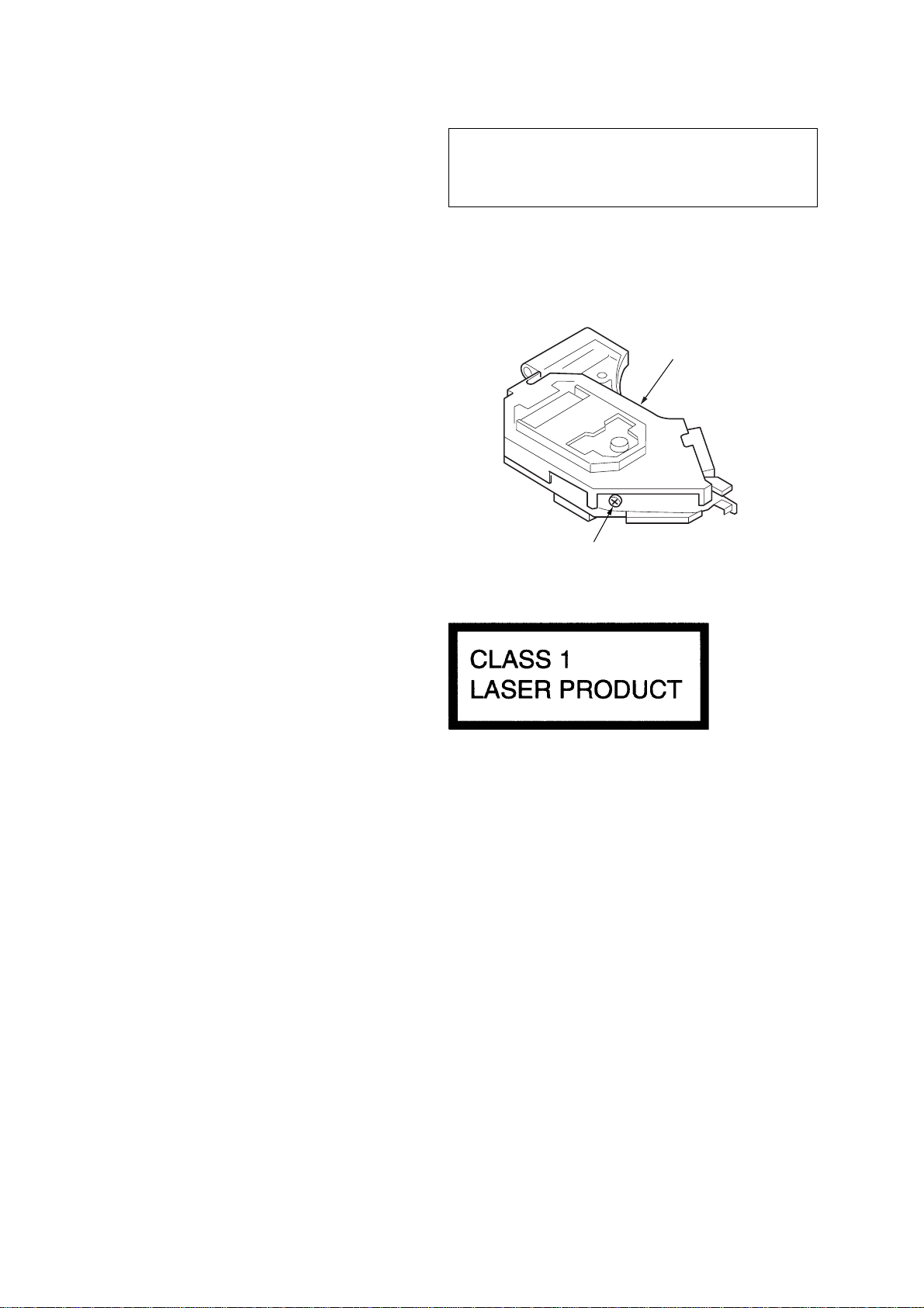
NOTES ON HANDLING THE OPTICAL PICK-UP BLOCK
OR BASE UNIT
The laser diode in the optical pick-up block may suffer electrostatic
breakdown because of the potential difference generated by the
charged electrostatic load, etc. on clothing and the human body.
During repair, pay attention to electrostatic breakdown and also use
the procedure in the printed matter which is included in the repair
parts.
The flexible board is easily damaged and should be handled with
care.
• US, Canadian model
CAUTION
Use of controls or adjustments or performance of procedures
other than those specified herein may result in hazardous
radiation exposure.
If the optical pick-up block is defective, please replace the whole
optical pick-up block.
Never turn the semi-fixed resistor located at the side of optical
pick-up block.
optical pick-up bloc
semi-fixed resistor
• AEP, UK model
NOTES ON LASER DIODE EMISSION CHECK
The laser beam on this model is concentrated so as to be focused on
the disc reflective surface by the objective lens in the optical pickup block. Therefore, when checking the laser diode emission, observe from more than 30 cm away from the objective lens.
Notes on Chip Component Replacement
• Never reuse a disconnected chip component.
• Notice that the minus side of a tantalum capacitor may be dam-
aged by heat.
TEST DISCS
This set can playback CD-R and CD-ROM discs. The following
test discs should be used to check the capability:
CD-R test disc TCD-R082LMT (Part No. J-2502-063-1)
CD-RW test disc TCD-W082L (Part No. J-2502-063-2)
SAFETY-RELATED COMPONENT WARNING!!
This label is located on the bottom of the chassis.
ATTENTION AU COMPOSANT AYANT RAPPORT
À LA SÉCURITÉ!!
COMPONENTS IDENTIFIED BY MARK 0 OR DOTTED LINE
WITH MARK 0 ON THE SCHEMATIC DIAGRAMS AND IN
THE PARTS LIST ARE CRITICAL TO SAFE OPERATION.
REPLACE THESE COMPONENTS WITH SONY P ARTS WHOSE
PART NUMBERS APPEAR AS SHOWN IN THIS MANUAL OR
IN SUPPLEMENTS PUBLISHED BY SONY.
2
LES COMPOSANTS IDENTIFIÉS P AR UNE MARQUE 0 SUR LES
DIAGRAMMES SCHÉMATIQUES ET LA LISTE DES PIÈCES
SONT CRITIQUES POUR LA SÉCURITÉ DE FONCTIONNEMENT.
NE REMPLACER CES COMPOSANTS QUE PAR DES PIÈCES
SONY DONT LES NUMÉROS SONT DONNÉS DANS CE MANUEL
OU DANS LES SUPPLÉMENTS PUBLIÉS PAR SONY.
CDX-M3DI/M1000TF
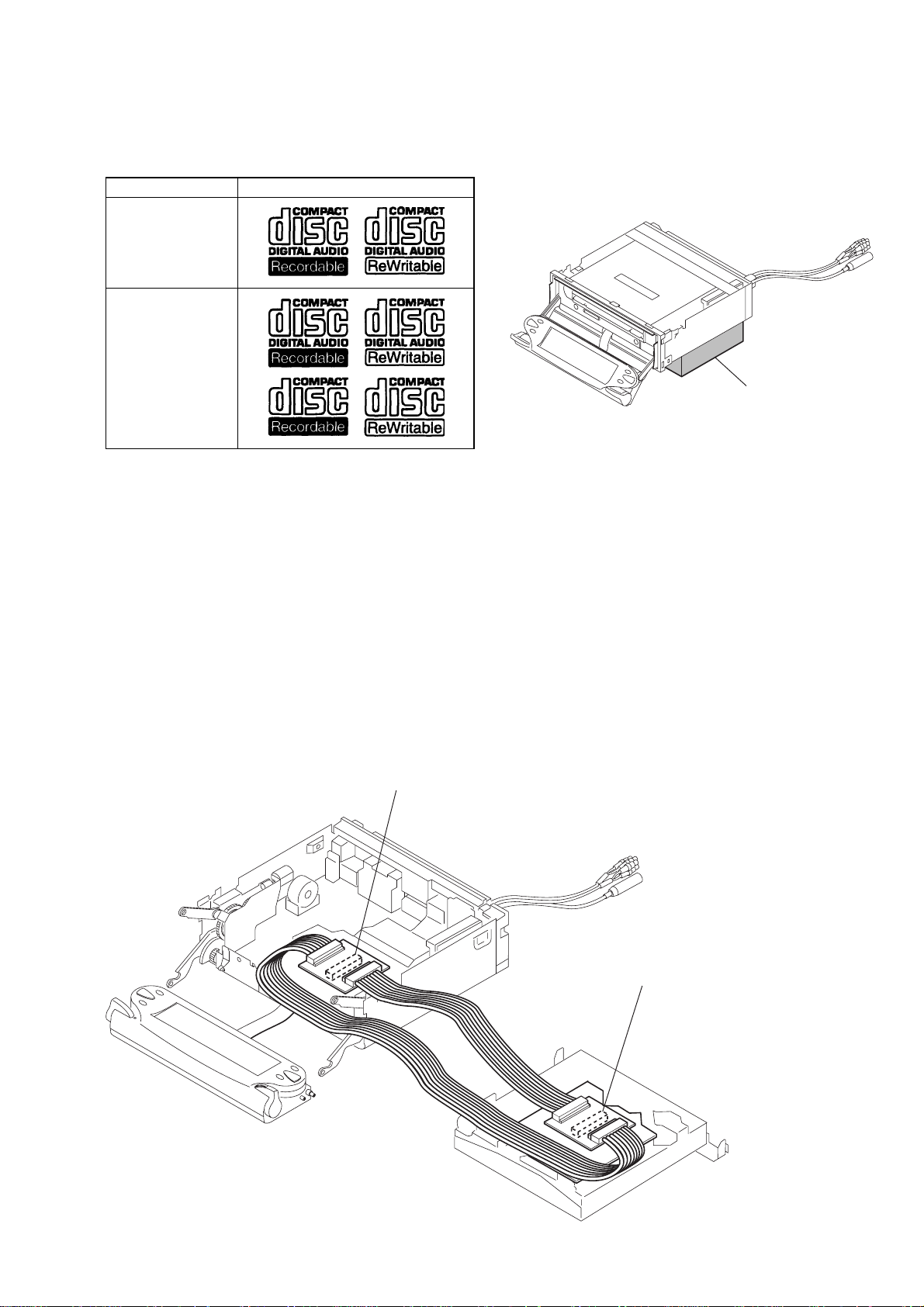
Notes on CD-Rs (recordable CDs)/CD-RWs (rewritable
CDs)
This unit can play the following discs:
Type of discs Label on the disc
Audio CD
MP3 files
• Some CD-Rs/CD-RWs (depending on the equipment used for
its recording or the condition of the disc) may not play on this
unit.
• You cannot play a CD-R/CD-RW that is not finalized∗.
• You can play MP3 files recorded on CD-ROMs, CD-Rs, and
CD-RWs.
• A CD-R/CD-RW to which a session can be added can be played.
∗ A process necessary for a recorded CD-R/CD-RW disc to be
played on the audio CD player.
EXTENSION CABLE AND SERVICE POSITION
When repairing or servicing this set, connect the jig (extension cable)
as shown below.
• Connect the MAIN board (CN402) and the SERV O board (CN1)
with the extension cable (Part No. J-2502-062-1).
NOTE FOR THE OPENING OF THE FRONT PANEL
In this set, the front panel is lowered to below the bottom face when
it is opened.
When servicing the set, place it on a stand having a height of about
2 cm.
stand
FORCED FRONT PANEL OPEN/CLOSE
The front panel is forced to OPEN/CLOSE at the timing that the
power (ACC) is turned off.
If the Z button for the front panel is not effective, the following
method is used:
With the front panel open: The front panel is closed when A CC is
switched from ON to OFF edge.
With the front panel closed:The front panel is opened when ACC
is switched from ON to OFF edge.
NOTE FOR REPLACEMENT OF THE DIGITAL BOARD
When repairing, the complete DIGITAL board should be replaced
since any parts in the DIGITAL board cannot be repaired.
MAIN BOARD CN402
SERVO BOARD CN1
3

CDX-M3DI/M1000TF
TABLE OF CONTENTS
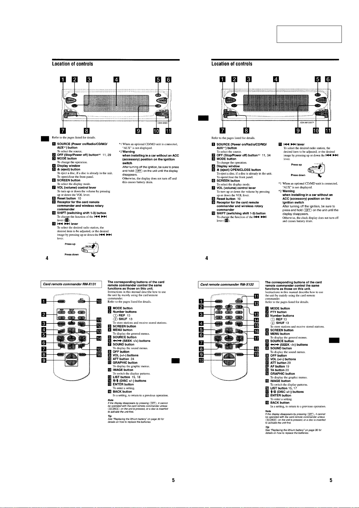
1. GENERAL
Location of Controls (CDX-M3DI) ........................................ 5
Location of Controls (CDX-M1000TF) ..................................5
Connections (CDX-M3DI) ...................................................... 6
Connections (CDX-M1000TF) ............................................... 7
2. DISASSEMBLY
2-1. Front Panel Assy ............................................................... 10
2-2. Sub Panel (CD) Assy......................................................... 10
2-3. CD Mechanism Block ....................................................... 11
2-4. Digital Board ..................................................................... 11
2-5. Cam Block Assy, Motor Block Assy................................. 12
2-6. Main Board ....................................................................... 12
2-7. Fan, Chassis Back ............................................................. 13
2-8. Chassis (T) Sub Assy ........................................................13
2-9. Lever Section..................................................................... 14
2-10. Servo Board....................................................................... 14
2-11. Shaft Roller Assy, Load SW Board ................................... 15
2-12. Floating Block Assy .......................................................... 16
2-13. Optical Pick-up Block ....................................................... 16
3. PHASE ALIGNMENT
3-1. Gear (Cam L) .................................................................... 17
3-2. Gear (Cam R) ....................................................................17
4. DIAGRAMS
4-1. IC Pin Descriptions ...........................................................18
4-2. Block Diagram –CD Section–........................................... 22
4-3. Block Diagram –Main Section–........................................ 23
4-4. Block Diagram –Display Section–.................................... 24
4-5. Circuit Boards Location ....................................................25
4-6. Printed Wiring Board –CD Mechanism Section (1/2)– ....26
4-7. Printed Wiring Boards –CD Mechanism Section (2/2)–... 27
4-8. Schematic Diagram –CD Mechanism Section (1/2)– .......28
4-9. Schematic Diagram –CD Mechanism Section (2/2)– .......29
4-10. Printed Wiring Board –Main Section (1/2)– ..................... 30
4-11. Printed Wiring Boards –Main Section (2/2)–.................... 31
4-12. Schematic Diagram –Main Section (1/4)– ........................ 32
4-13. Schematic Diagram –Main Section (2/4)– ........................ 33
4-14. Schematic Diagram –Main Section (3/4)– ........................ 34
4-15. Schematic Diagram –Main Section (4/4)– ........................ 35
4-16. Printed Wiring Boards –Display Section– ........................ 36
4-17. Schematic Diagram –Display Section–............................. 37
4-18. IC Block Diagrams............................................................ 38
5. EXPLODED VIEWS
5-1. Chassis Section ................................................................. 42
5-2. Cam Section ......................................................................43
5-3. Main Board Section .......................................................... 44
5-4. Front Panel Section ...........................................................45
5-5. CD Mechanism Section (1) ............................................... 46
5-6. CD Mechanism Section (2) ............................................... 47
5-7. CD Mechanism Section (3) ............................................... 48
6. ELECTRICAL PARTS LIST ........................................49
4
CDX-M3DI/M1000TF
SECTION 1
GENERAL
(CDX-M3DI) (CDX-M1000TF)
This section is extracted
from instruction manual.
5

CDX-M3DI/M1000TF
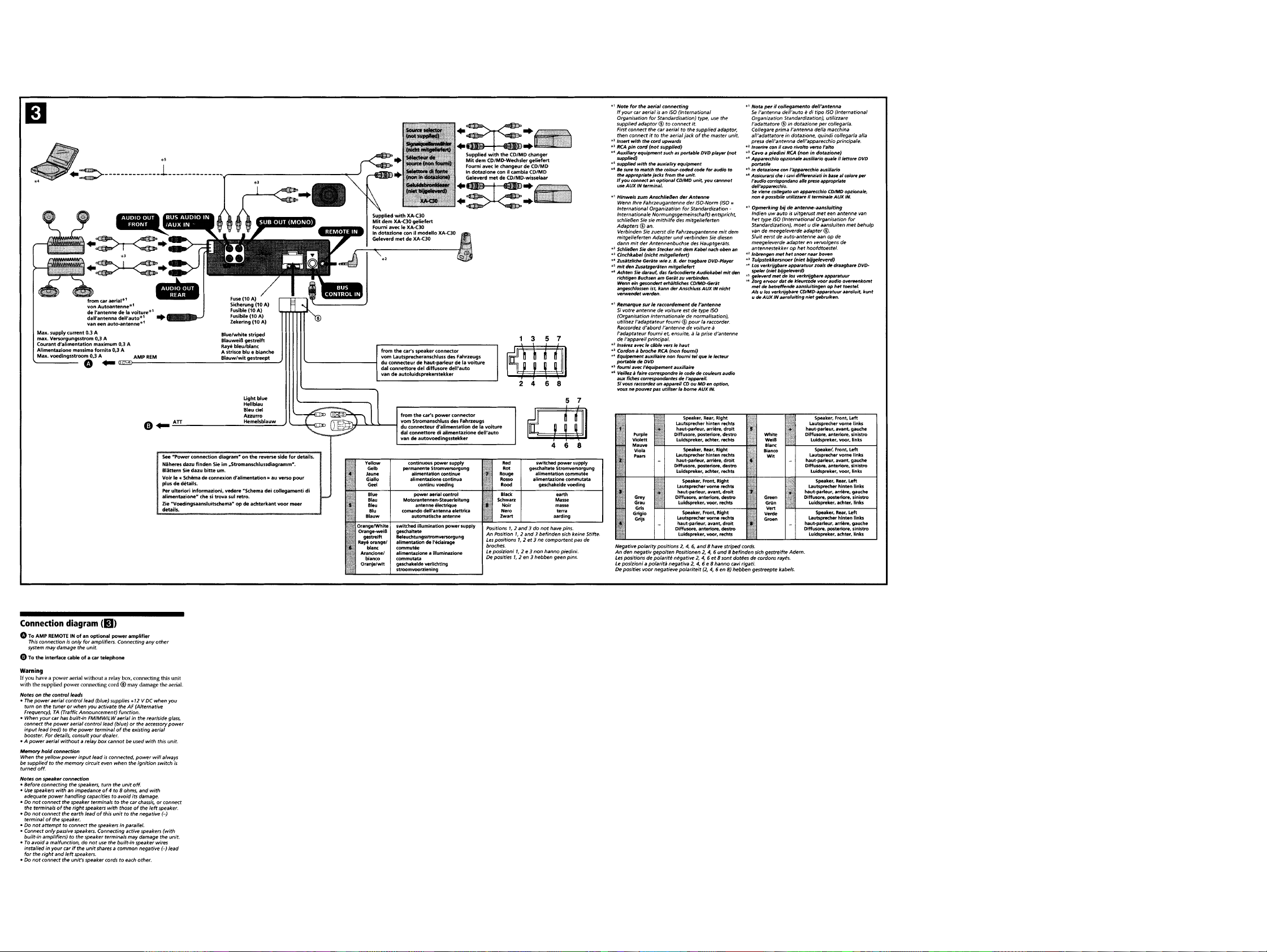
Connections (CDX-M3DI)
6
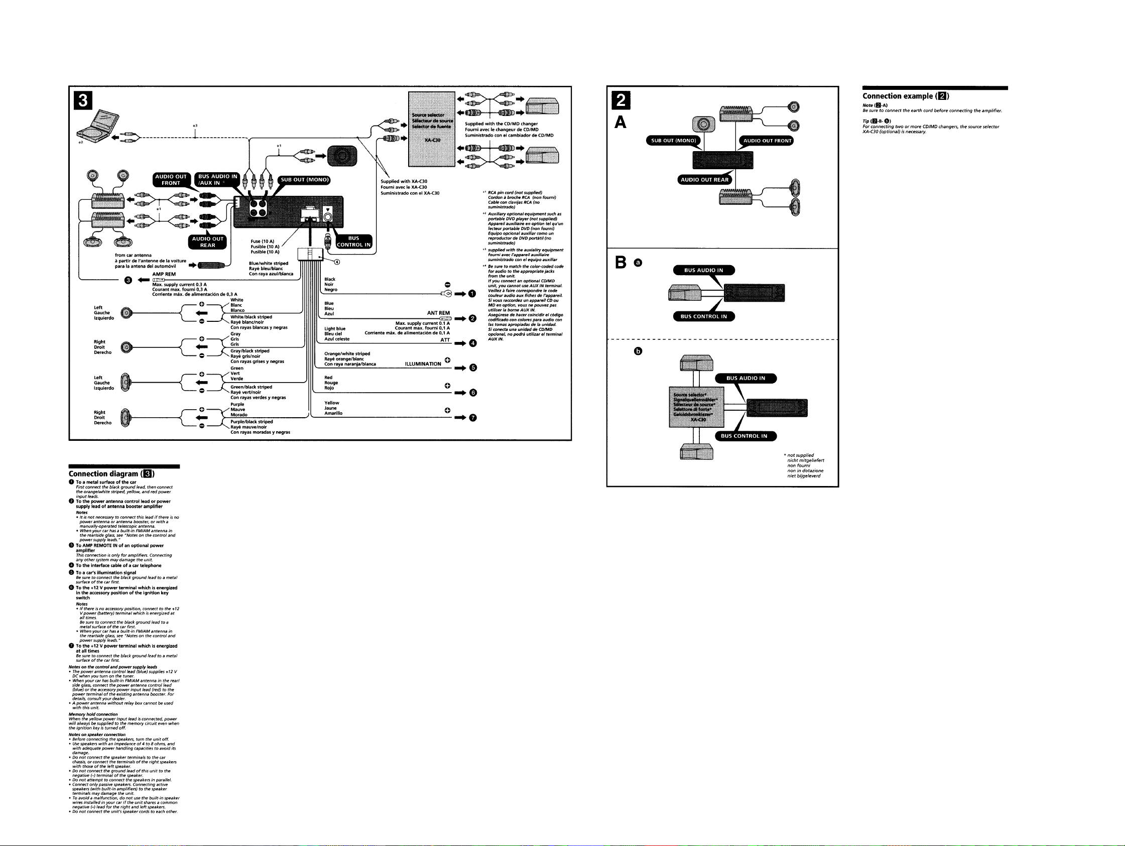
Connections (CDX-M1000TF)
CDX-M3DI/M1000TF
77
CDX-M3DI/M1000TF
88
SECTION 2
DISASSEMBLY
Note : This set can be disassemble according to the following sequence.
SET
CDX-M3DI/M1000TF
2-1. FRONT PANEL ASSY
(Page 10)
2-2. SUB PANEL (CD) ASSY
(Page 10)
2-3. CD MECHANISM BLOCK
(Page 11)
2-4. DIGITAL BOARD
(Page 11)
2-5. CAM BLOCK ASSY,
MOTOR BLOCK ASSY
(Page 12)
2-6. MAIN BOARD
(Page 12)
2-7. FAN, CHASSIS BACK
(Page 13)
2-8. CHASSIS (T) SUB ASSY
(Page 13)
2-9. LEVER SECTION
(Page 14)
2-11. SHAFT ROLLER ASSY,
LOAD SW BOARD
(Page 15)
2-12. FLOATING BLOCK ASSY
(Page 16)
2-13. OPTICAL PICK-UP BLOCK
(Page 16)
2-10. SERVO BOARD
(Page 14)
9
CDX-M3DI/M1000TF
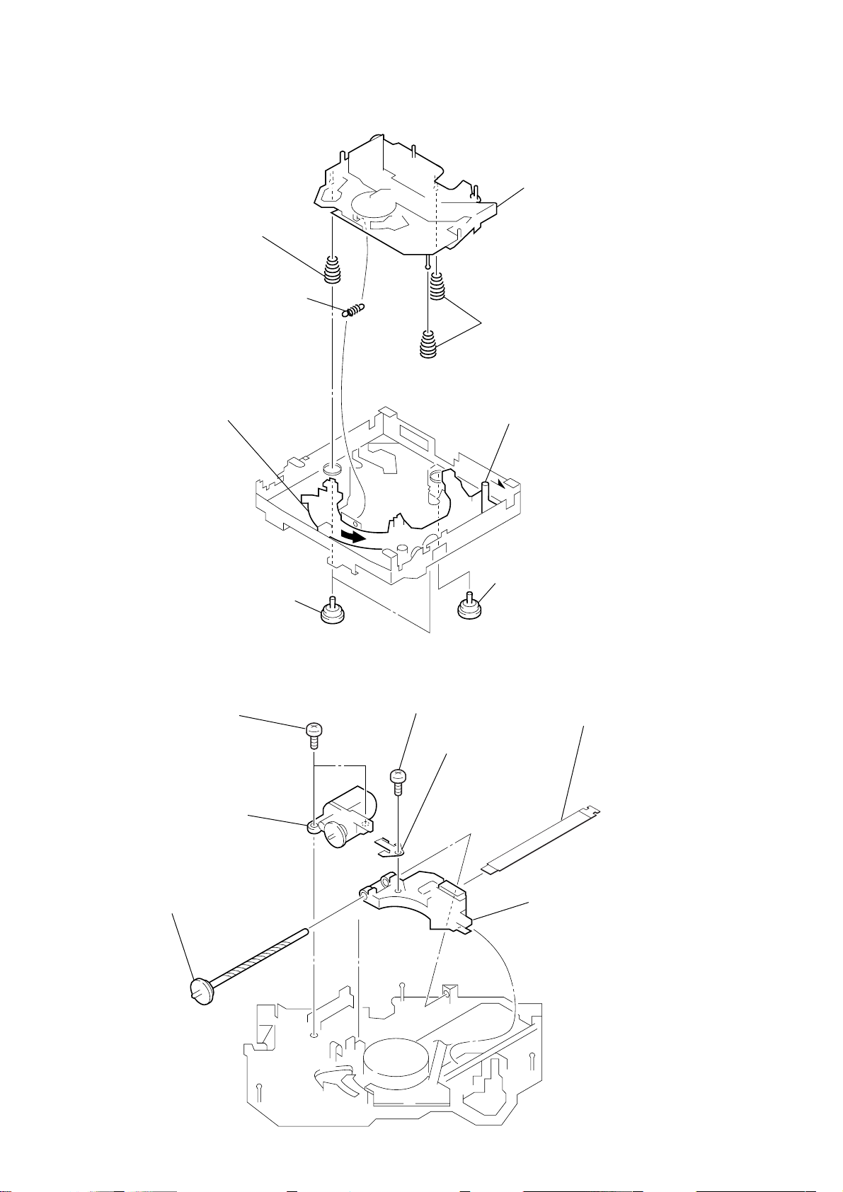
Note : Follow the disassembly procedure in the numerical order given.
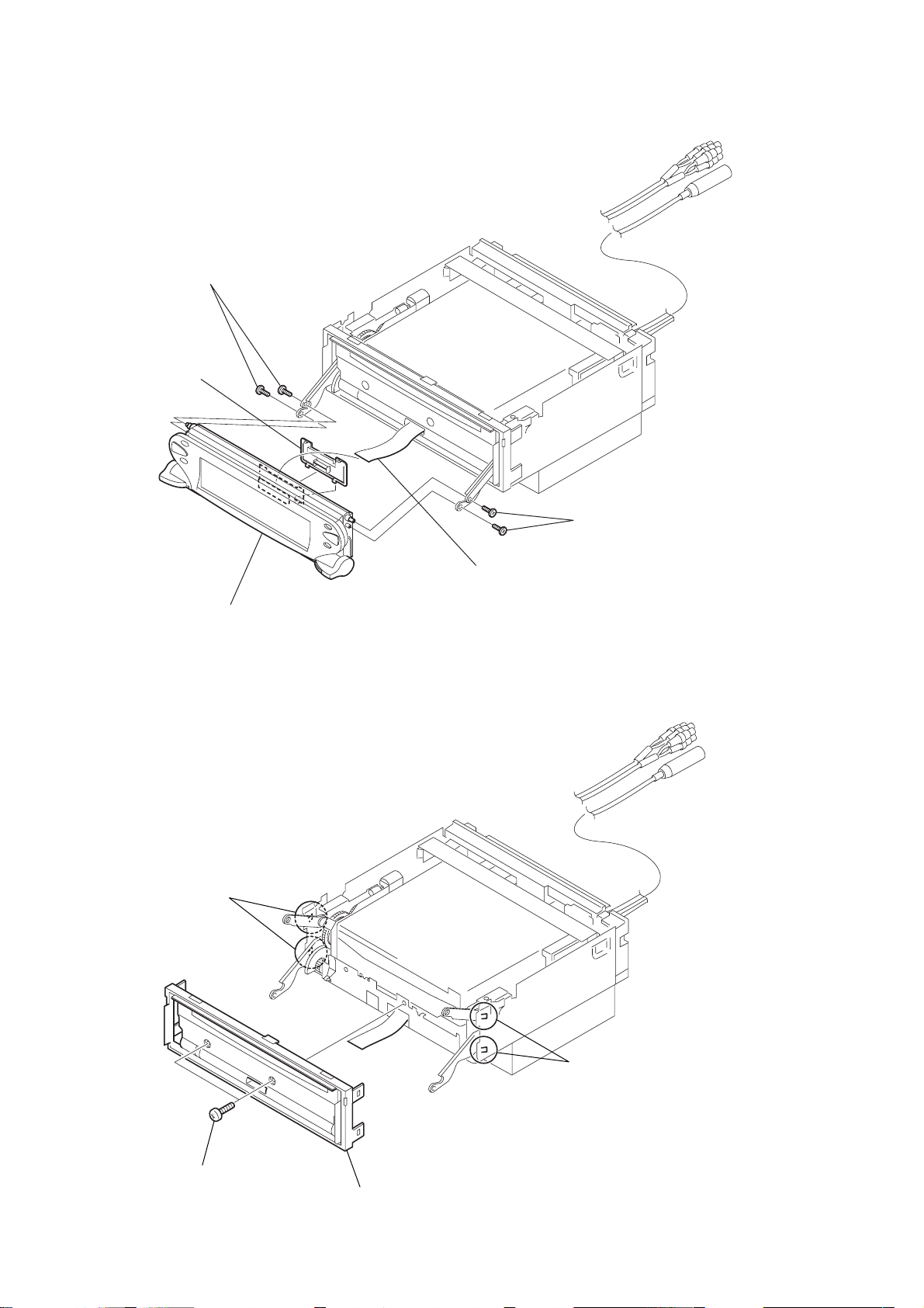
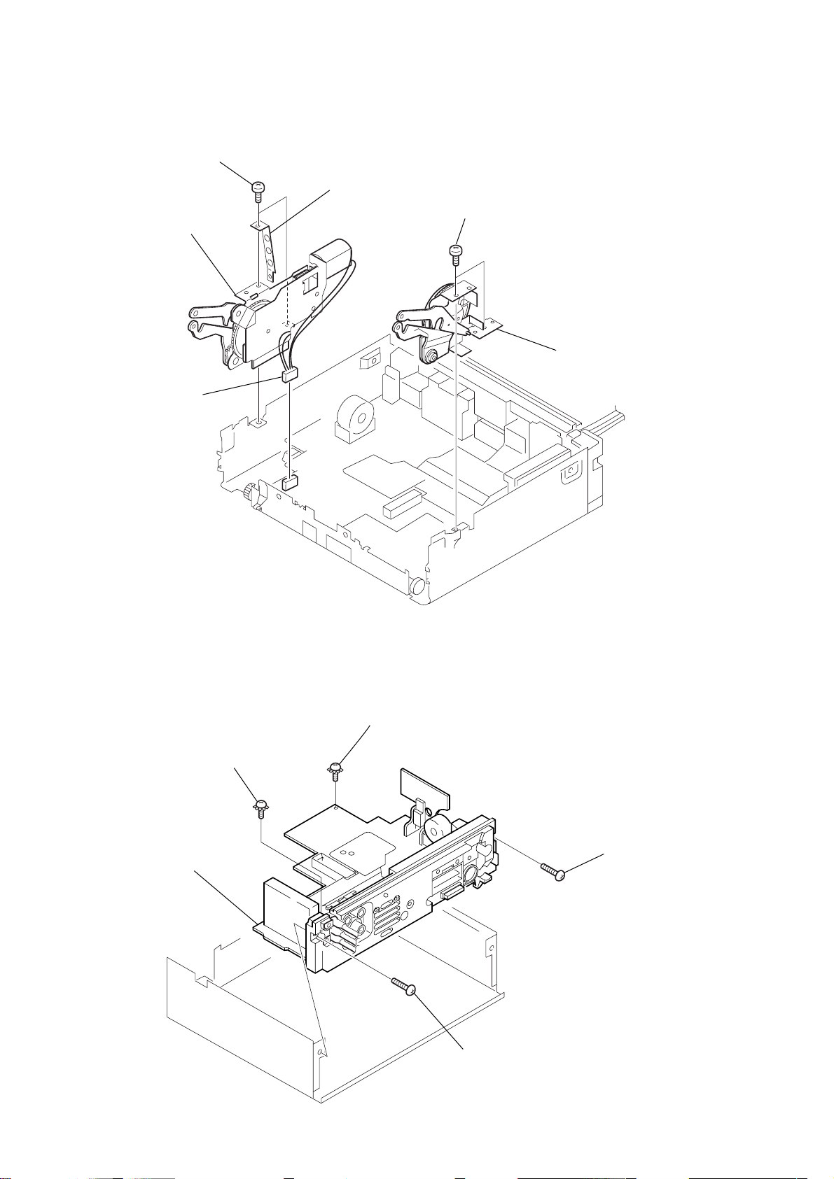
2-1. FRONT PANEL ASSY
1
screws (thin head M1.4)
3
cover (FPC)
5
2-2. SUB PANEL (CD) ASSY
3
claws
front panel assy
2
screws (thin head M1.4)
4
CN201
(Take care not to pull the
flexible board excessively)
10
1
PTT 2.6x6
4
sub panel (CD) assy
2
claws
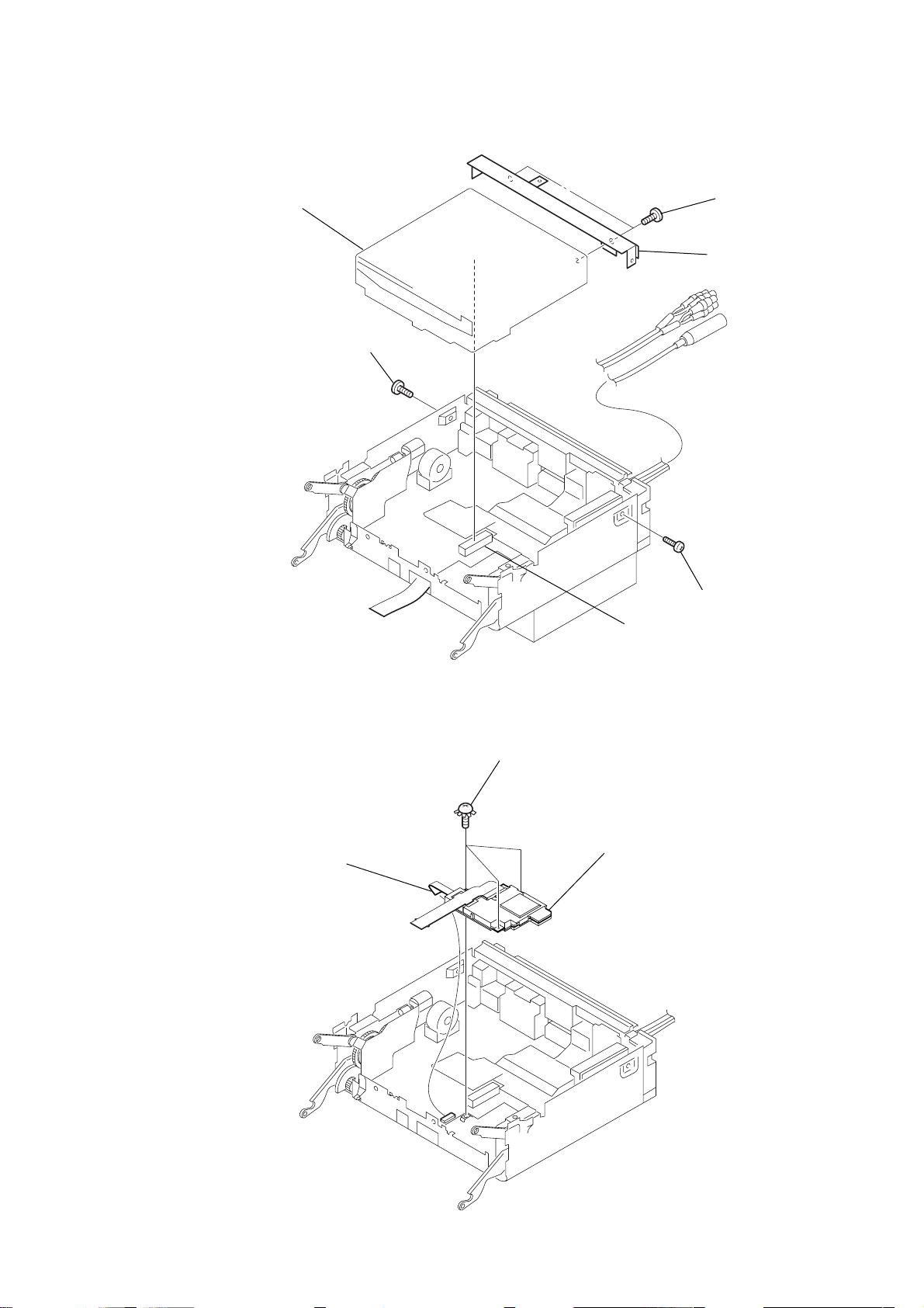
2-3. CD MECHANISM BLOCK
3
DIGITAL board
1
CN801
2
PTT 2.6x6
ground point
4
CD mechanism block
2
PTT 2.6x4
CDX-M3DI/M1000TF
5
PTT 2.6x6
6
bracket (CD)
2-4. DIGITAL BOARD
3
CN402
1
PTT 2.6x4
11
CDX-M3DI/M1000TF
8
2-5. CAM BLOCK ASSY, MOTOR BLOCK ASSY
4
PTT 2.6x6
5
6
motor block assy
3
CN601
cover (protection)
1
PTT 2.6x6
2
cam block assy
2-6. MAIN BOARD
5
MAIN board
4
PTT 2.6x6
ground point
3
PTT 2.6x6
ground point
2
PTT 2.6x8
1
PTT 2.6x
12
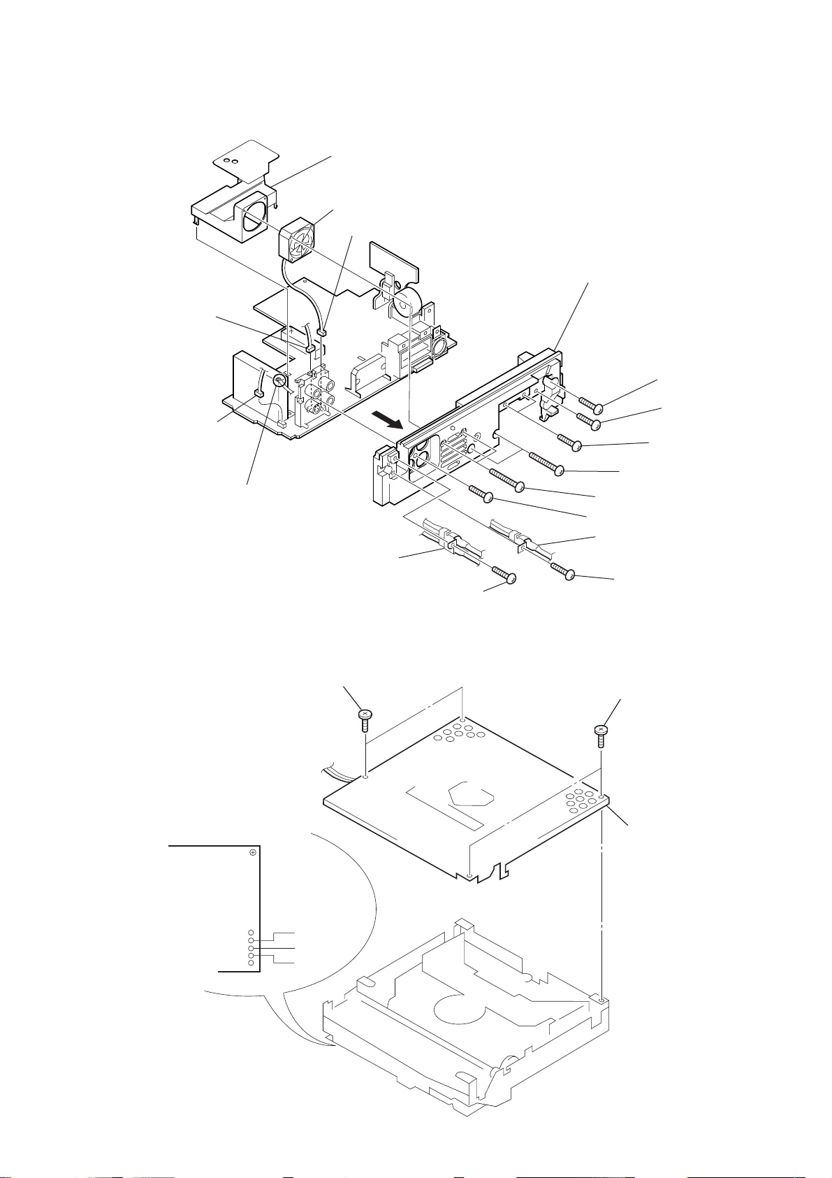
2-7. FAN, CHASSIS BACK
8
y
3
CN302
7
CN201
qf
duct (fan) assy
qg
fan
qh
CN802
CDX-M3DI/M1000TF
qj
heat sink
qs
PTT 2.6x8
qa
PTT 2.6x
0
PTT 2.6x8
6
Removal the solder.
2-8. CHASSIS (T) SUB ASSY
1
Unsoldering three lead wires.
2
2
P 2x3
cord
1
PTT 2.6x8
9
qd
PTP 2x18
8
PTT 2.6x8
5
cord
4
3
PTT 2.6x12
PTT 2.6x8
P 2x3
4
chassis (T) sub ass
SERVO board
(SIDE A)
black
red
white
13
CDX-M3DI/M1000TF
2-9. LEVER SECTION
6
lever (R)
3
tension spring (LR)
7
5
guide (disc)
lever (L)
1
special screw
2
DISC IN SW board
2-10. SERVO BOARD
3
Removal the solders.
5
P2x3
4
two claws
7
special screws
1
CN3
9
SERVO board
8
special screw
2
CN2
4
Unsolder the
lead wires.
black
yellow
14
6
loading motor assy
optical pick-up block
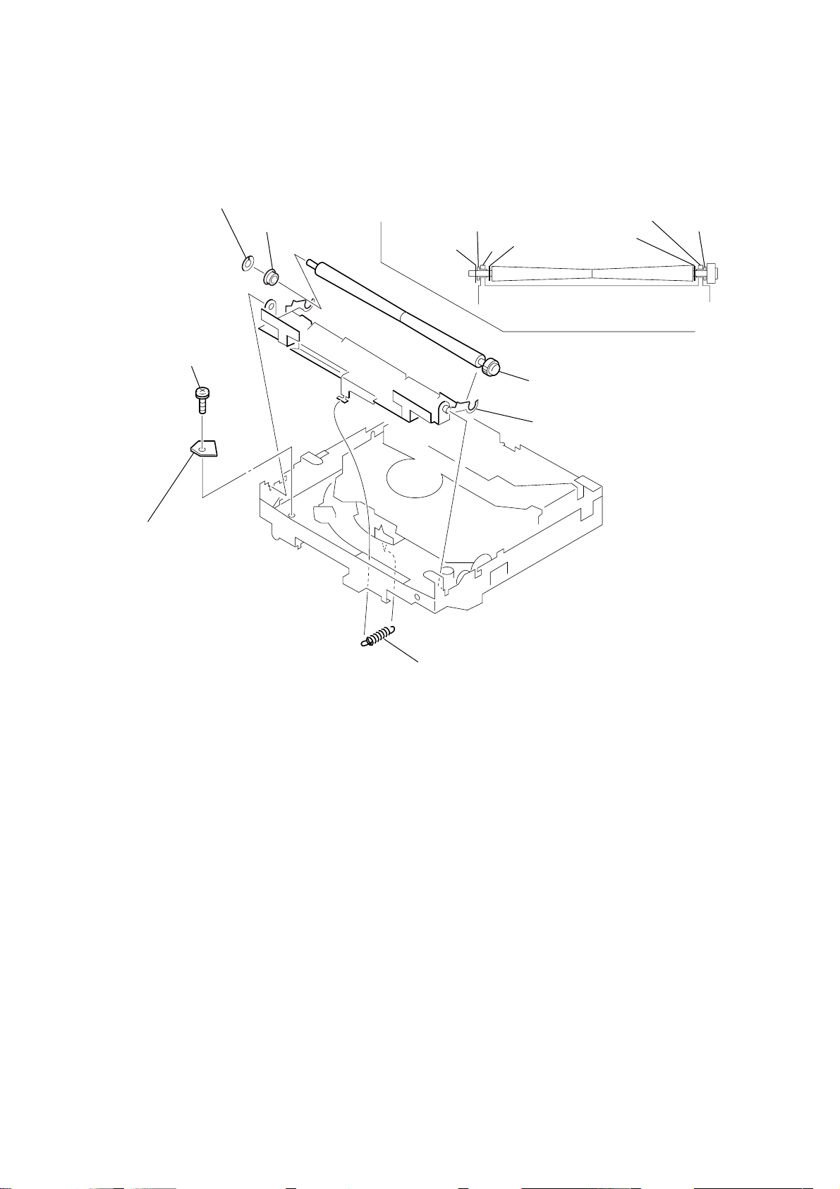
2-11. SHAFT ROLLER ASSY, LOAD SW BOARD
• When installing, take note of the positions
arm (roller) and washers. (Fig. 1)
3
6
special screw
retaining ring
(RA)
4
shaft retainer
(roller)
retaining ring (RA)
shaft retainer (roller)
washer
arm
5
shaft roller assy
2
arm
(roller)
Fig. 1
CDX-M3DI/M1000TF
arm
washer
shaft retainer (roller)
7
LOAD SW board
1
tension spring (RA)
15
CDX-M3DI/M1000TF
2-12. FLOATING BLOCK ASSY
7
compression spring (FL)
1
tension spring (KF1)
5
Turn loading ring in the
direction of the arrow.
6
floating block assy
8
compression spring (FL)
4
Fit lever (D) in the direction of the arrow.
3
damper (T)
2-13. OPTICAL PICK-UP BLOCK
1
P 2x3
2
sled motor assy (M902)
6
shaft (feed) assy
3
P 2x3
4
plate spring (feed)
2
damper (T)
7
PICK-UP FLEXIBLE board
5
optical pick-up (KSS-721A)
16
SECTION 3
6
g
y
PHASE ALIGNMENT
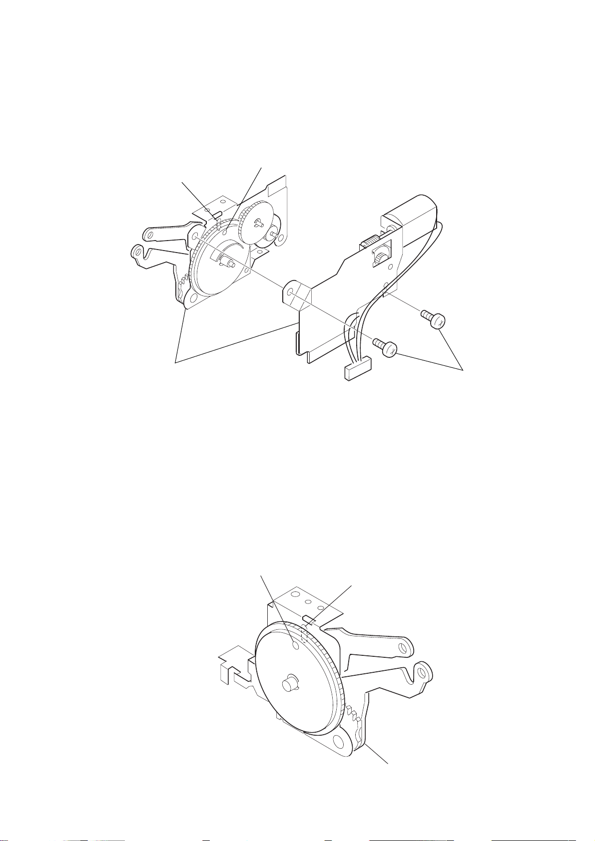
3-1. GEAR (CAM L)
•Align the gear (cam L) position setting hole with the center mark on
the bracket before screwing the motor block assy to the mechanism
chassis.
gear (cam L) position setting hole
center mark
CDX-M3DI/M1000TF
1
motor block assy
2
PTT 2.6x
3-2. GEAR (CAM R)
1 Align the gear (cam R) position setting hole with the center mark
on the bracket before screwing the cam block assy to the
mechanism chassis.
2 Touch the gear (cam R) with fingers in the direction of rotation
and make sure that there is no phase difference with the R-side
position setting hole.
ear (cam R) position setting hole
center mark
cam block ass
17

CDX-M3DI/M1000TF
SECTION 4
DIAGRAMS
4-1. IC PIN DESCRIPTIONS
• IC5 CXD9684R-005 (DSP) (SERVO Board (1/2))
Pin No. Pin Name I/O Pin Description
1 /RESET I Reset signal input (L: reset)
2MIMD I Microcomputer interface mode selection signal input (H: I2C, L: TSB) (Fixed at H)
3, 4 AD0, AD1 O External S-RAM address signal output 0, 1
5 MIDIO (I2C_SDA) I/O Serial data input/output
6 MICK (I2C_SCL) I Serial clock signal input
7 AD2 O External S-RAM address signal output 2
8 VDDT (3.3V) — Power supply pin (+3.3 V) for digital circuit
9 SDO O Data output 0
10, 11 AD3, AD4 O External S-RAM address signal output 3, 4
12 SDI0 I Data input 0
13 BCKIA I Bit clock signal input A
14 LRCKIA I LR clock signal input A
15 AD5 O External S-RAM address signal output 5
16 CE O External S-RAM chip enable signal output
17 OE O External S-RAM output enable signal output
18 VDD (2.5V) — Power supply pin (+2.5 V) for digital circuit
19 STANDBY I Standby mode control signal input (H: STB, L: normal)
20 VSS (2.5GND) — Ground for digital circuit
21 VSSL (2.5GND) — Ground for DAC L-ch
22 VRAL — Reference voltage pin for DAC L-ch
23 LO O DAC L-ch signal output (Open)
24 VDAL (2.5V) — Power supply pin (+2.5 V) for DAC L-ch
25 VDAR (2.5V) — Power supply pin (+2.5 V) for DAC R-ch
26 RO O DAC R-ch signal output (Open)
27 VRAR — Reference voltage pin for DAC R-ch
28 VSSR (2.5GND) — Ground for DAC R-ch
29 TESTP I Test pin (H: test mode, L: normal) (Fixed at L)
30 CKS I VCO selection signal input (H: VCO, L: X1 input) (Fixed at H)
31 to 34 AD12 to AD9 O External S-RAM address signal output 12 to 9
35 VDDT (3.3V) — Power supply pin (+3.3 V) for digital circuit
36 to 38 AD8 to AD6 O External S-RAM address signal output 8 to 6
39 REQ O Interrupt request signal output for CD master control IC
40 VSS — Ground for digital circuit
41, 42 AD13, AD14 O External S-RAM address signal output 13, 14
43 WR O External S-RAM write signal output
44, 45 AD16, AD15 O External S-RAM address signal output 16, 15
46, 47 IO0, IO1 I/O External S-RAM data input/output 0, 1
48 VSS — Ground for digital circuit
49 to 51 IO2 to IO4 I/O External S-RAM data input/output 2 to 4
52 VDD (2.5V) — Power supply pin (+2.5 V) for digital circuit
53 to 55 IO5 to IO7 I/O External S-RAM data input/output 5 to 7
56 VSSP — Ground for VCO circuit
57 PDO O PLL phase error detection signal output
58 VCOI I VCO control voltage input
59 VDDP — Power supply pin (+2.5 V) for VCO circuit
60 XRDE I/O External clock input/audio clock output (Open)
61 VDDX (2.5V) — Power supply pin (+2.5 V) for oscillation circuit
62 XI I Resonator input
63 XO O Resonator output
64 VSSX — Ground for oscillation circuit
18
 Loading...