

Sony CDX-L550X, CDX-L570X Service manual
CDX-L550X/L570X
SERVICE MANUAL
Ver 1.0 2001. 01
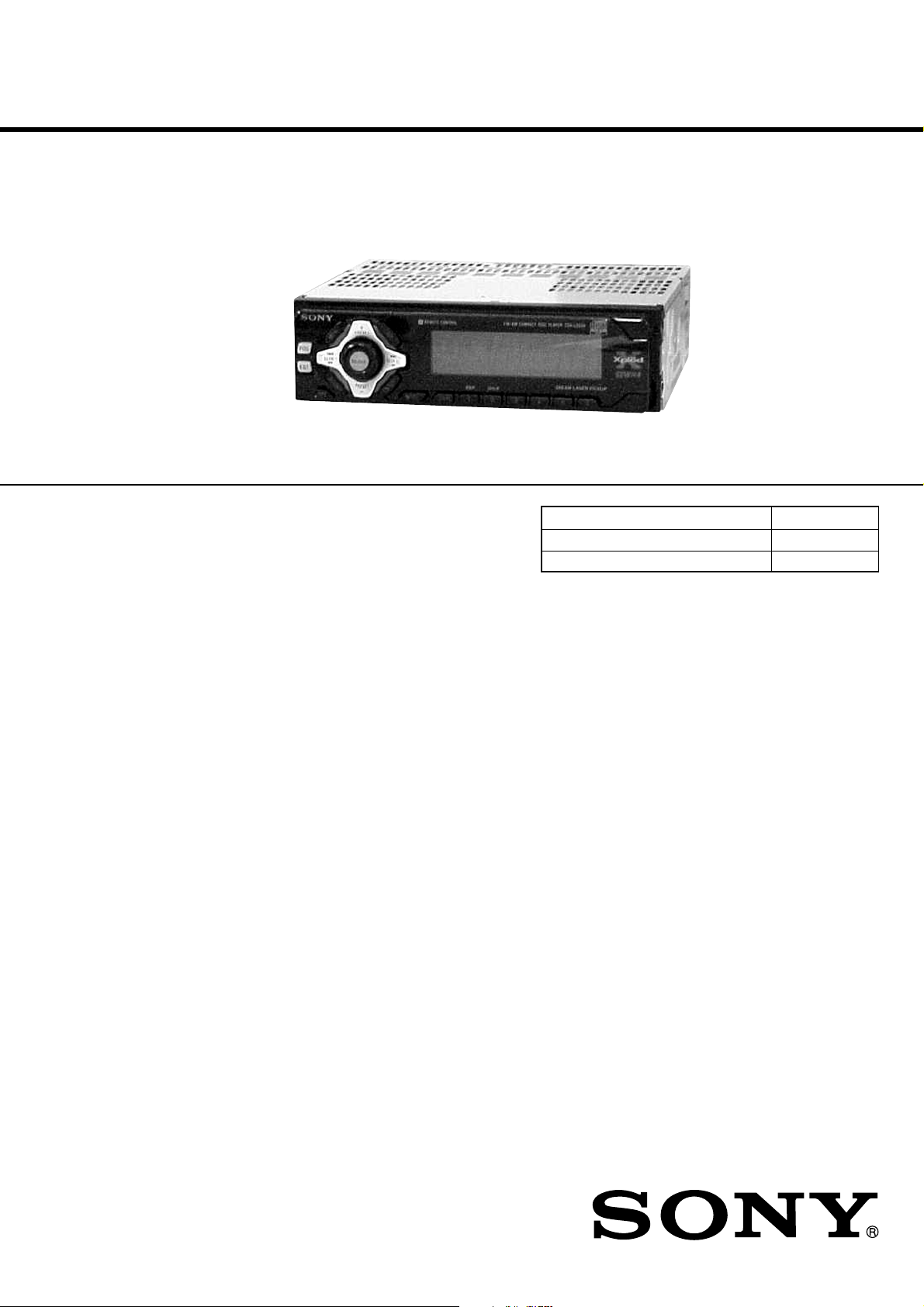
Photo: CDX-L550X
• The tuner and CD sections have no adjustments.
AUDIO POWER SPECIFICATIONS (US Model)
POWER OUTPUT AND TOTAL HARMONIC DISTORTION
23 watts per channel minimum continuous average power into
4 ohms, 4 channels driven from 20 Hz to 20 kHz with no more
than 5% total harmonic distortion.
CD player section
Signal-to-noise ratio 90 dB
Frequency response 10 – 20,000 Hz
Wow and flutter Below measurable limit
Laser Diode Properties (US, Canadian Model)
Material GaAlAs
Wavelength 780 nm
Emission Duration Continuous
Laser output power Less than 44.6 µW*
* This output is the value measured at a distance
of 200 mm from the objective lens surface on the
Optical Pick-up Block.
Tuner section
FM
Tuning range 87.5 – 107.9 MHz (US, Canadian model)
FM tuning interval (E Model):
50 kHz/200 kHz switchable
87.5 – 108 MHz (at 50 kHz step)
87.5 – 107.9 MHz (at 200 kHz step)
Antenna terminal External Antenna connector
Intermediate frequency 10.7 MHz/450 kHz
Usable sensitivity 8 dBf
Selectivity 75 dB at 400 kHz
Signal-to-noise ratio 66 dB (stereo),
72 dB (mono)
Harmonic distortion at 1 kHz
0.6% (stereo),
0.3% (mono)
Separation 35 dB at 1 kHz
Frequency response 30 – 15,000 Hz
AM
Tuning range 530 – 1,710 kHz (US, Canadian model)
AM tuning interval (E model):
9 kHz/10 kHz switchable
531 – 1,602 kHz (at 9 kHz step)
530 – 1,710 kHz (at 10 kHz step)
Antenna terminal External Antenna connector
Intermediate frequency 10.7 MHz/450 kHz
Sensitivity 30 µV
SPECIFICATIONS
US Model
Canadian Model
CDX-L550X
E Model
CDX-L570X
Model Name Using Similar Mechanism NEW
CD Drive Mechanism Type MG-393X-121//K
Optical Pick-up Name KSS-720A
Power amplifier section
Outputs Speaker outputs
(sure seal connectors)
Speaker impedance 4 – 8 ohms
Maximum power output 52 W × 4 (at 4 ohms)
General
Outputs Audio outputs
Power Antenna relay control lead
Power amplifier control lead
Input Telephone ATT control lead
Tone controls Bass ±10 dB at 62 Hz (US, Canadian model)
Bass ±8 dB at 100 Hz (E model)
Treble ±10 dB at 16 kHz (US, Canadian model)
Treble ±8 dB at 10 kHz (E model)
Loudness (E model) +8 dB at 100 Hz
+2 dB at 10 kHz
Power requirements 12 V DC car battery
(negative ground)
Dimensions Approx. 178 × 50 × 176 mm
(7 1/8 × 2 × 7 in.) (w/h/d)
Mounting dimensions Approx. 182 × 53 × 161 mm
(7 1/4 × 2 1/8 × 6 3/8 in.) (w/h/d)
Mass Approx. 1.2 kg
(2 lb. 10 oz.)
Supplied accessories Parts for installation and connections (1 set)
Front panel case (1)
Note
This unit cannot be connected to a digital preamplifier or an equalizer.
Design and specifications are subject to change without
notice.
FM/AM COMPACT DISC PLAYER
9-870-255-11
2001A0400-1
© 2001. 1
Sony Corporation
Audio Entertainment Group
General Engineering Dept.
1
CDX-L550X/L570X
k
SERVICE NOTES
CAUTION
Use of controls or adjustments or performance of procedures
other than those specified herein may result in hazardous
radiation exposure.
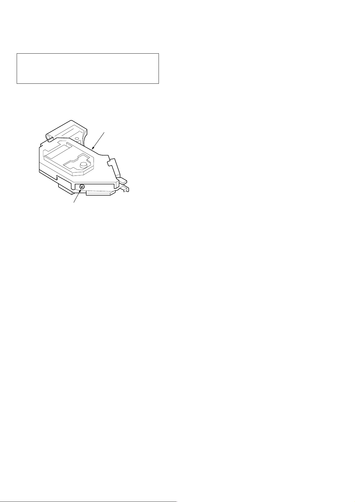
If the optical pick-up block is defective, please replace the whole
optical pick-up block.
Never turn the semi-fixed resistor located at the side of optical
pick-up block.
optical pick-up bloc
semi-fixed resistor
NOTES ON HANDLING THE OPTICAL PICK-UP BLOCK
OR BASE UNIT
The laser diode in the optical pick-up block may suffer electrostatic
breakdown because of the potential difference generated by the
charged electrostatic load, etc. on clothing and the human body.
During repair, pay attention to electrostatic breakdown and also use
the procedure in the printed matter which is included in the repair
parts.
The flexible board is easily damaged and should be handled with
care.
TABLE OF CONTENTS
1. GENERAL
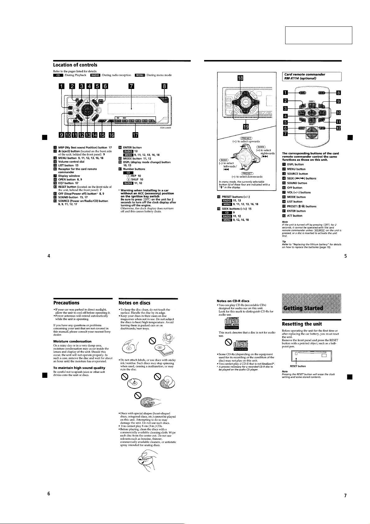
Location of controls................................................................. 3
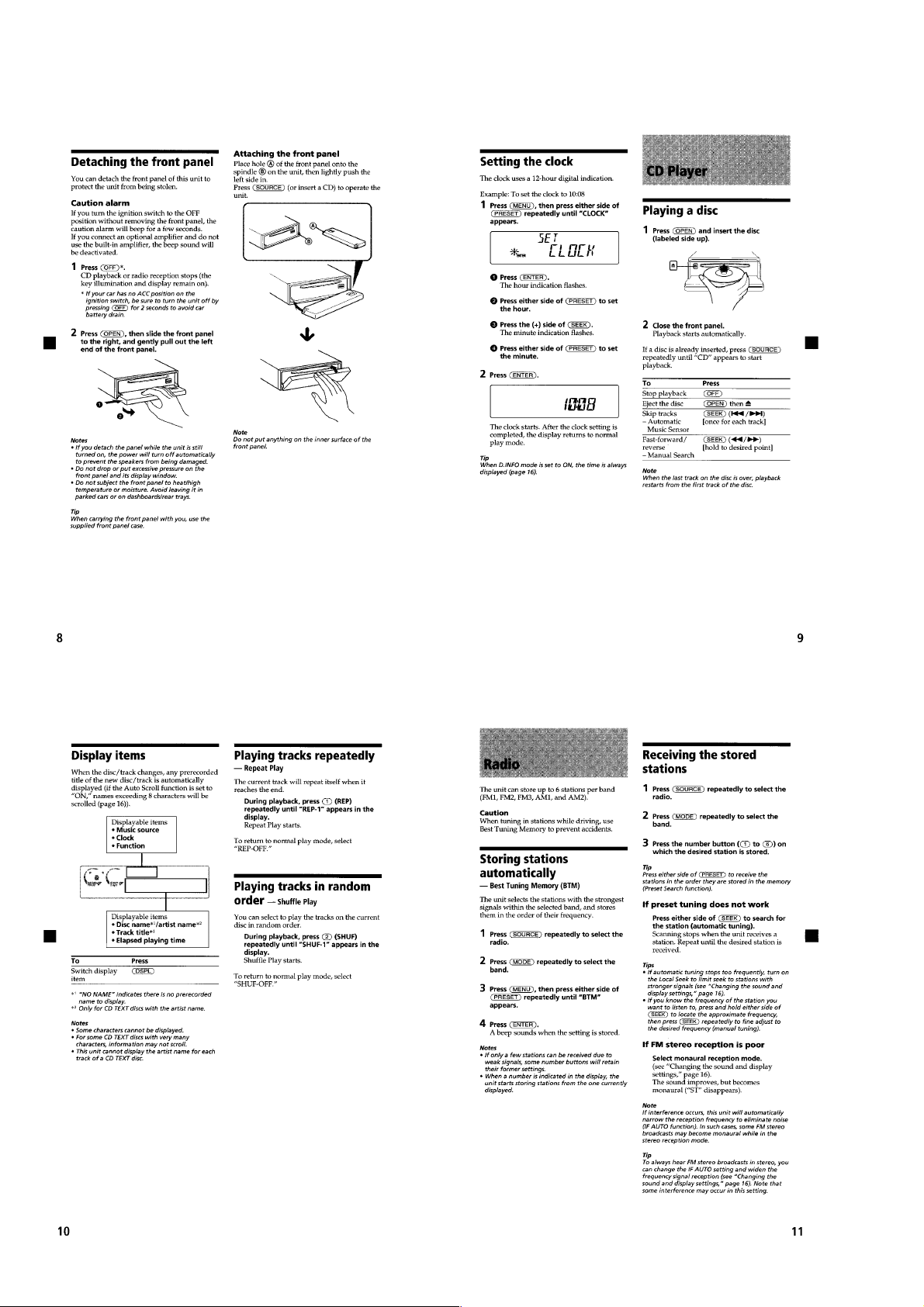
Getting Started......................................................................... 3
CD Player ................................................................................ 4
Radio ....................................................................................... 4
Other Functions ....................................................................... 5
Connection Diagram................................................................ 7
2. DISASSEMBLY
2-1. Sub Panel (CD) Assy........................................................... 8
2-2. CD Mechanism Block .........................................................8
2-3. Main Board ......................................................................... 8
2-4. Heat Sink (Main)................................................................. 9
2-5. Chassis (T) Sub Assy .......................................................... 9
2-6. Lever Section .................................................................... 10
2-7. Servo Board....................................................................... 10
2-8. Arm Roller Assy ................................................................ 11
2-9. Floating Block ................................................................... 11
2-10. Optical Pick-up Block ....................................................... 12
3. DIAGRAMS
3-1. IC Pin Descriptions ........................................................... 13
3-2. Block Diagram –CD Section–........................................... 15
3-3. Block Diagram –Tuner Section–....................................... 16
3-4. Block Diagram –Display Section–.................................... 17
3-5. Circuit Boards Location .................................................... 17
3-6. Printed Wiring Boards –CD Mechanism Section–............ 18
3-7. Schematic Diagram –CD Mechanism Section– ................ 20
3-8. Printed Wiring Boards –Main Section– ............................ 21
3-9. Schematic Diagram –Main Section (1/2)– ........................ 22
3-10. Schematic Diagram –Main Section (2/2)– ........................ 23
3-11. Printed Wiring Board –Relay Section– ............................. 24
3-12. Schematic Diagram –Relay Section–................................ 25
3-13. Schematic Diagram –Display Section–............................. 26
3-14. Printed Wiring Board –Display Section– ..........................27
NOTES ON LASER DIODE EMISSION CHECK
The laser beam on this model is concentrated so as to be focused on
the disc reflective surface by the objective lens in the optical pickup block. Therefore, when checking the laser diode emission, observe from more than 30 cm away from the objective lens.
Notes on Chip Component Replacement
• Never reuse a disconnected chip component.
• Notice that the minus side of a tantalum capacitor may be dam-
aged by heat.
4. EXPLODED VIEWS
4-1. Chassis Section ................................................................. 30
4-2. Front panel Section ........................................................... 31
4-3. CD Mechanism Section (1) ............................................... 32
4-4. CD Mechanism Section (2) ............................................... 33
4-5. CD Mechanism Section (3) ............................................... 34
5. ELECTRICAL PARTS LIST ........................................ 35
SAFETY-RELATED COMPONENT WARNING!!
COMPONENTS IDENTIFIED BY MARK 0 OR DOTTED LINE
WITH MARK 0 ON THE SCHEMATIC DIAGRAMS AND IN
THE PARTS LIST ARE CRITICAL TO SAFE OPERATION.
REPLACE THESE COMPONENTS WITH SONY P ARTS WHOSE
PART NUMBERS APPEAR AS SHOWN IN THIS MANUAL OR
IN SUPPLEMENTS PUBLISHED BY SONY.
ATTENTION AU COMPOSANT AYANT RAPPORT
À LA SÉCURITÉ!!
LES COMPOSANTS IDENTIFIÉS P AR UNE MARQUE 0 SUR LES
DIAGRAMMES SCHÉMATIQUES ET LA LISTE DES PIÈCES
SONT CRITIQUES POUR LA SÉCURITÉ DE FONCTIONNEMENT.
NE REMPLACER CES COMPOSANTS QUE PAR DES PIÈCES
SONY DONT LES NUMÉROS SONT DONNÉS DANS CE MANUEL
OU DANS LES SUPPLÉMENTS PUBLIÉS PAR SONY.
2
SECTION 1
GENERAL
CDX-L550X/L570X
This section is extracted
from instruction manual.
3
CDX-L550X/L570X
4
CDX-L550X/L570X
5
CDX-L550X/L570X
6
CDX-L550X/L570X
77
CDX-L550X/L570X
8
6
SECTION 2
DISASSEMBLY
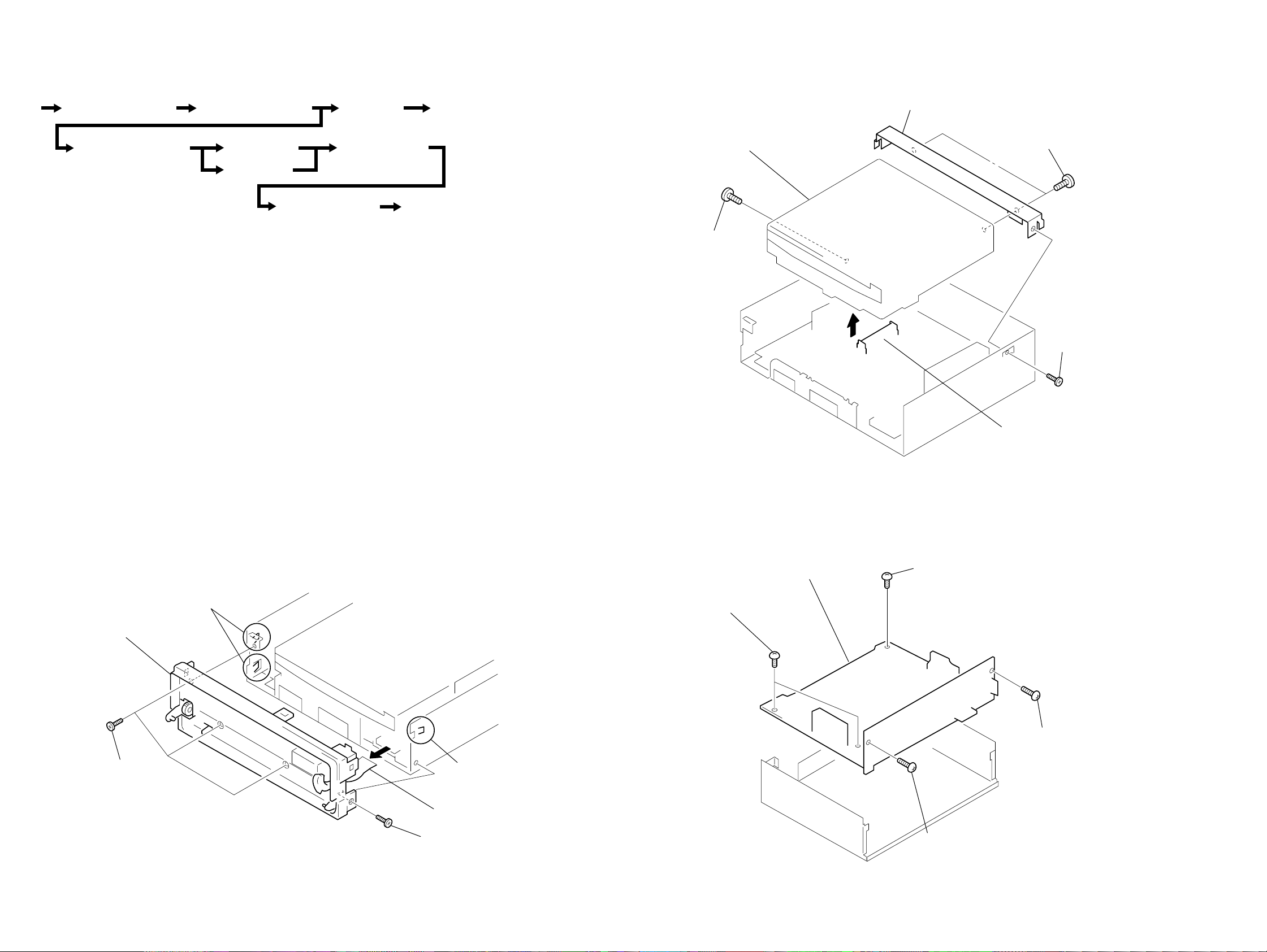
Note : This equipiment can be removed usiing the following procedure.
Set Sub Panel (CD) Assy CD Mechanism Block
Chassis (T) Sub Assy Lever Section
Servo Board
Floating Block Assy Optical Pick-up Block
Main Board Heat Sink (Main)
Arm Roller Assy
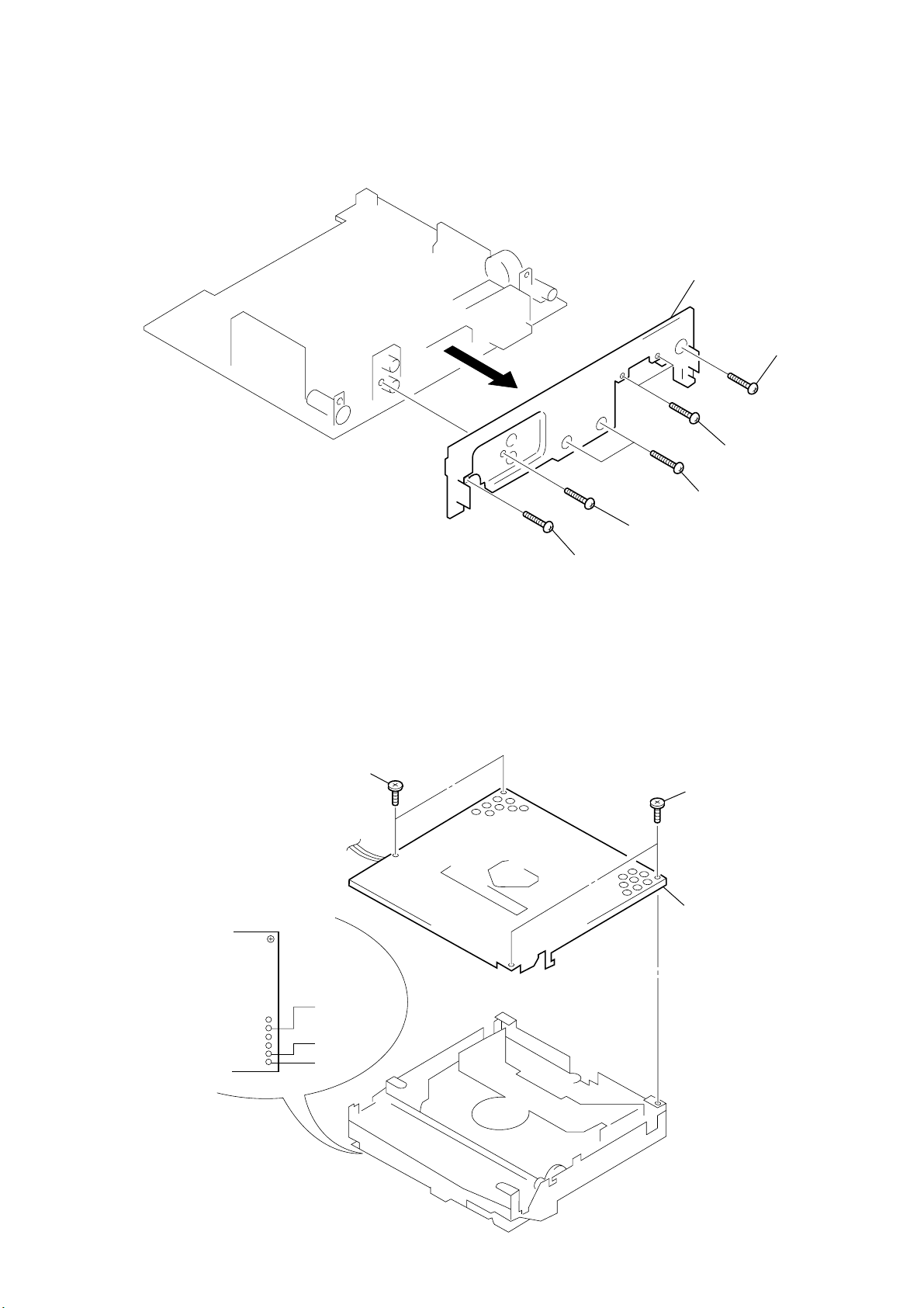
2-2. CD MECHANISM BLOCK
5 CD mechanism block
2 PTT 2.6x6
7 bracket (CD)
6 PTT 2.6x6
3
1 PTT 2.6x
Note : Follow the disassembly procedure in the numerical order given.
2-1. SUB PANEL (CD) ASSY
4 two claws
6 sub panel (CD) assy
2-3. MAIN BOARD
4 screws (+BTT)
5 MAIN board
4 CNP701
3 screw (+BTT)
2 PTT 2.6x
2 PTT 2.6x6
3 claw
1 PTT 2.6x6
5 CNP802
1 PTT 2.6x8
88
6 heat sink (main)
1 PTT 2.6x8
2 PTT 2.6x8
4 PTT 2.6x8
3 PTT 2.6x12
5 PTT 2.6x8
2-4. HEAT SINK (MAIN)
CDX-L550X/L570X
2-5. CHASSIS (T) SUB ASSY
1 Unsolder the
lead wires.
2 P 2x3
black
red
white
3 P 2x3
4 chassis (T) sub assy
9
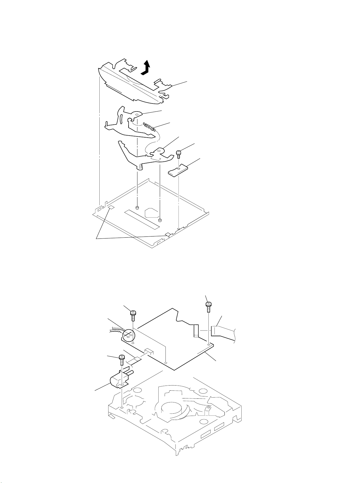
CDX-L550X/L570X
2-6. LEVER SECTION
5 guide (disc)
6 lever (R)
3 tension spring (LR)
7 lever (L)
1 special screw
2 IN SELF SW board
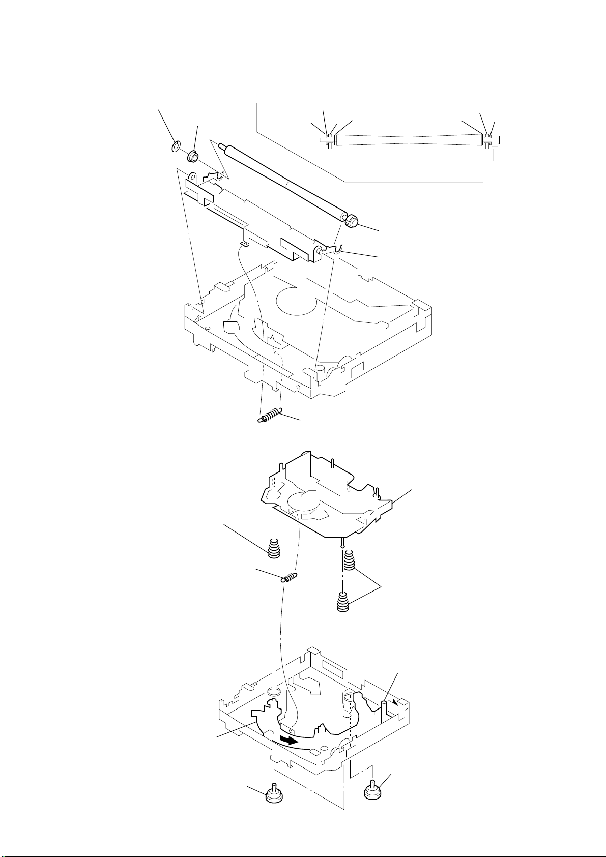
2-7. SERVO BOARD
4 claws
6 special screw
3 Removal the solders.
1 CN3
4 P 2x3
5 loading motor assy
7 special screw
2 CN2
8 SERVO board
10
)
2-8. ARM ROLLER ASSY
• When installing, take note of the positions
arm (roller) and washers. (Fig. 1)
CDX-L550X/L570X
3 retaing ring (RA)
4 shaft retainer
(roller)
shaft retainer (roller)
retaing ring (RA)
arm
washer
Fig. 1
5 shaft roller assy
2 arm (roller)
washer
arm
shaft retainer (roller
2-9. FLOATING BLOCK ASSY
7 compression spring (FL)
1 tension spring (KF1)
1 tension spring (RA)
6 floating block assy
8 compression spring (FL)
4 Fit lever (D) in the
direction of the arrow.
5 Turn loading ring in the
direction of the arrow.
3 damper (T)
2 damper (T)
11
CDX-L550X/L570X
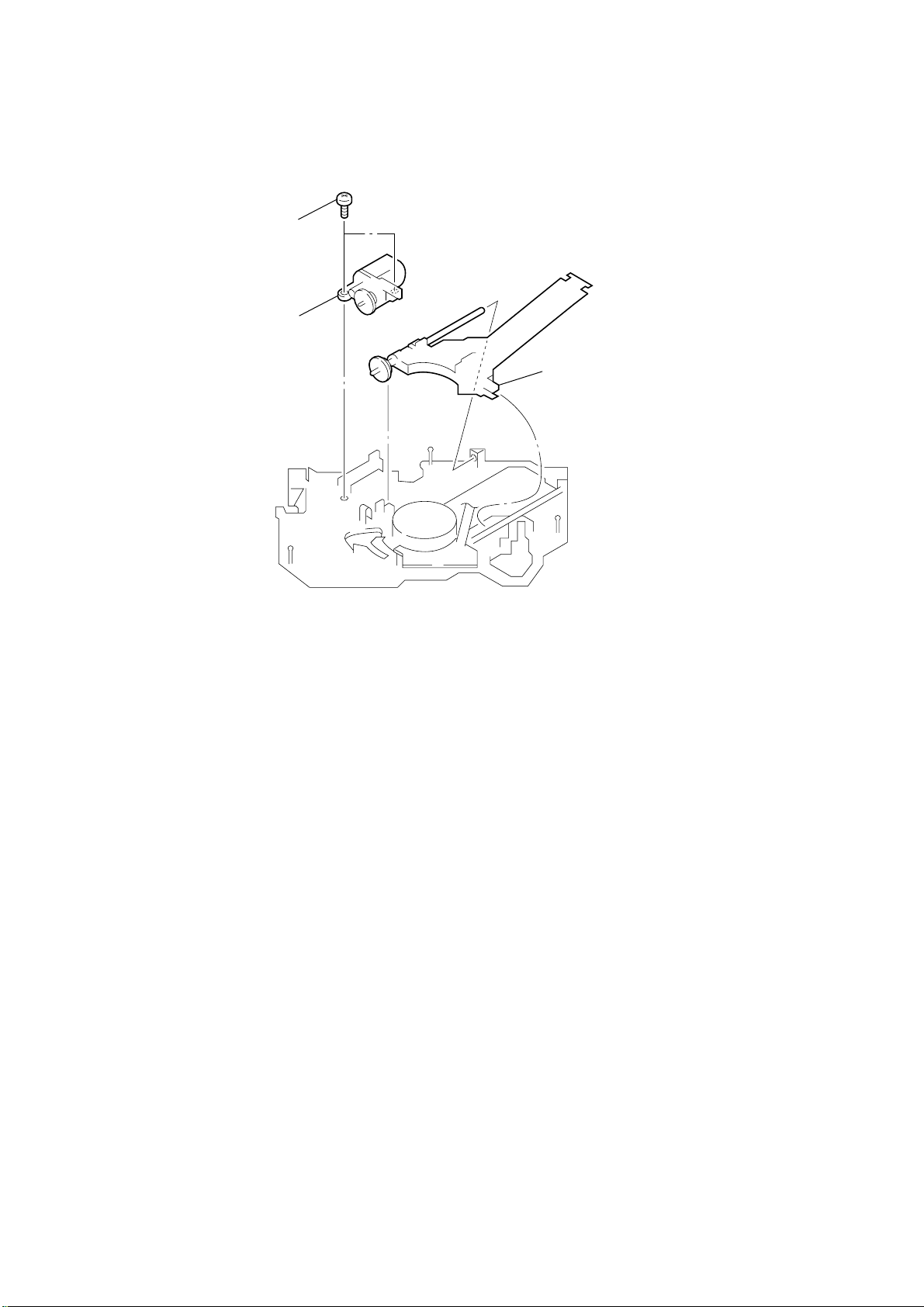
2-10. OPTICAL PICK-UP BLOCK
1 P 2x3
2 sled motor assy
3 optical pick-up block
12
CDX-L550X/L570X
SECTION 3
DIAGRAMS
3-1. IC PIN DESCRIPTION
• IC801 MN101C49KTG1 (SYSTEM CONTROL)
Pin No. Pin Name I/O Pin Description
1 VREF– — Ground for A/D converter power supply
2 VSM I S-meter voltage detection signal input from tuner unit (TU601)
3 NIL I Connect to ground.
4 KEYIN1 I Key signal input
5 KEYIN0 I Key signal input
6 RC IN0 I Rotary commander key signal input from remote in jack (CNP801)
7, 8 NIL I Not used. (Connect to ground.)
9 DSTSEL I Destination set up detection signal input (“L”: CDX-L550X, “H”: CDX-L570X)
10 VREF+ — A/D converter power supply
11 VDD — Power supply (+5 V) input pin
12 OSCOUT O High speed clock signal output (18.432 MHz)
13 OSCIN I High speed clock signal input (18.432 MHz)
14 VSS — Ground for power supply
15 XIN I Low speed clock signal input (32.768 kHz)
16 XOUT O Low speed clock signal output (32.768 kHz)
17 MMOD I
18 LCDSO O LCD serial data signal output to LCD driver (IC501)
19 LCDCE O LCD chip enable signal output to LCD driver (IC501)
20 LCDCKO O LDC serial clock signal output to LCD driver (IC501)
21 CD SO/TSO O CD servo IC serial data signal output
22 CD SI/TSI I CD servo IC serial data signal input
23 CD CKO/TCKO O CD servo IC serial clock signal output
24 SYSRST O System reset signal output to bus interface (IC803)
25 BUS ON O Bus on signal output to bus interface (IC803)
26 KEYACK I Key acknowledge detection signal input
27 NIL I Not used. (Connect to ground.)
28 BU IN I Back up current detection signal input
29 SIRCS I Remote signal input from remote control receiver (IC502)
30 CD SELFSW I CD mechanism self load position detection switch signal input from self switch (SW2)
31 CD PACK I CD text pack sync signal input from CD servo (IC1)
32 NIH I Connect to power supply.
33 RESET I microcomputer reset signal input from reset IC (IC802) “L”: reset
34 NOSE SW I Front panel attachment detection signal input from nose detect switch (S902) “L”: ON
35 BEEP O Beep signal output to power amp (IC404)
36 NCO O Not used. (Open)
37 TESTIN I Test mode detection signal input
38 ACCIN I Accessory power supply detection signal input
39 NCO O Not used. (Open)
40 TELA TT I Telephone ATT detection signal input
41 NIH I Connect to power supply.
42 BUSSO O Sony-Bus serial data signal output to bus interface (IC803)
43 BUSSI I Sony-Bus serial data signal input from bus interface (IC803)
44 BUSCKO O Sony-Bus serial clock signal output to bus interface (IC803)
45 I2CSIO I/O I2C bus serial data signal input/output
46 NCO O Not used. (Open)
47 I2CCKO O I2C bus serial clock signal output
48 NCO O Not used. (Open)
49 TUNON O Tuner power supply control signal output to power supply (IC901)
50 PW ON O System power supply control signal output to power supply (IC901)
Memory mode select signal input (Input to “Low” (single chip mode).)
(Connect to ground.)
13
 Loading...