

Sony CDXL-480-N Service manual
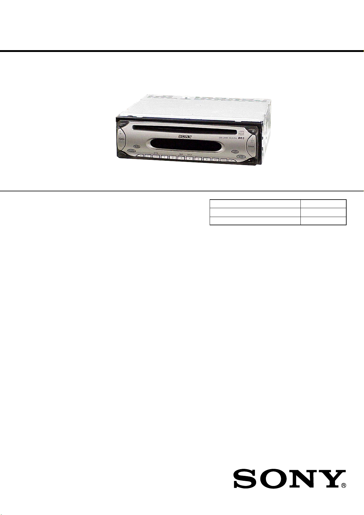
CDX-L480N
SERVICE MANUAL
Ver 1.0 2003. 07
• The tuner and CD sections have no adjustments.
Thai Model
Model Name Using Similar Mechanism CDX-L480X
CD Drive Mechanism Type MG-393XC-121//Q
Optical Pick-up Name KSS-721A
9-961-055-01
2003G04-1
© 2003. 07
FM/AM COMPACT DISC PLAYER
Sony Corporation
e Vehicle Company
Published by Sony Engineering Corporation
1

CDX-L480N
NOTES ON HANDLING THE OPTICAL PICK-UP BLOCK
OR BASE UNIT
The laser diode in the optical pick-up block may suffer electrostatic
breakdown because of the potential difference generated by the
charged electrostatic load, etc. on clothing and the human body.
During repair, pay attention to electrostatic breakdown and also use
the procedure in the printed matter which is included in the repair
parts.
The flexible board is easily damaged and should be handled with
care.
NOTES ON LASER DIODE EMISSION CHECK
The laser beam on this model is concentrated so as to be focused on
the disc reflective surface by the objective lens in the optical pickup block. Therefore, when checking the laser diode emission, observe from more than 30 cm away from the objective lens.
Notes on Chip Component Replacement
• Never reuse a disconnected chip component.
• Notice that the minus side of a tantalum capacitor may be dam-
aged by heat.
TEST DISCS
This set can playback CD-R and CD-ROM discs. The following
test discs should be used to check the capability:
CD-R test disc TCD-R082LMT (Part No. J-2502-063-1)
CD-RW test disc TCD-W082L (Part No. J-2502-063-2)
SAFETY-RELATED COMPONENT WARNING!!
COMPONENTS IDENTIFIED BY MARK 0 OR DOTTED LINE
WITH MARK 0 ON THE SCHEMATIC DIAGRAMS AND IN
THE PARTS LIST ARE CRITICAL TO SAFE OPERATION.
REPLACE THESE COMPONENTS WITH SONY P ARTS WHOSE
PART NUMBERS APPEAR AS SHOWN IN THIS MANUAL OR
IN SUPPLEMENTS PUBLISHED BY SONY.
2
z
MAIN BOARD
CNP301
J-2502-011-1
SERVO BOARD
CN1
UNLEADED SOLDER
Boards requiring use of unleaded solder are printed with the lead
free mark (LF) indicating the solder contains no lead.
(Caution: Some printed circuit boards may not come printed with
the lead free mark due to their particular size.)
: LEAD FREE MARK
Unleaded solder has the following characteristics.
• Unleaded solder melts at a temperature about 40°C higher than
ordinary solder.
Ordinary soldering irons can be used but the iron tip has to be
applied to the solder joint for a slightly longer time.
Soldering irons using a temperature regulator should be set to
about 350°C.
Caution: The printed pattern (copper foil) may peel away if the
heated tip is applied for too long, so be careful!
• Strong viscosity
Unleaded solder is more viscous (sticky, less prone to flow)
than ordinary solder so use caution not to let solder bridges
occur such as on IC pins, etc.
• Usable with ordinary solder
It is best to use only unleaded solder but unleaded solder may
also be added to ordinary solder.
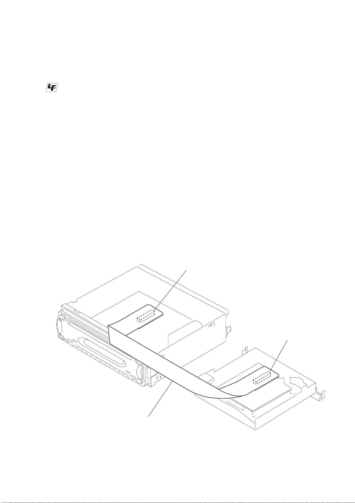
CDX-L480N
EXTENSION CABLE AND SERVICE POSITION
When repairing or servicing this set, connect the jig (extension cable)
as shown below.
• Connect the MAIN board (CNP301) and the SER V O board (CN1)
with the extension cable (Part No. J-2502-011-1).
3

CDX-L480N
TABLE OF CONTENTS
1. DISASSEMBLY
1-1. Sub Panel Assy.................................................................... 5
1-2. CD Mechanism Block ......................................................... 6
1-3. Main Board ......................................................................... 6
1-4. Heat Sink .............................................................................7
1-5. Chassis (T.U) Assy .............................................................. 7
1-6. Disc in Board ...................................................................... 8
1-7. Servo Board......................................................................... 8
1-8. Shaft Roller Assy ................................................................ 9
1-9. Floating Block Assy ............................................................9
1-10. Optical Pick-up Block ....................................................... 10
2. DIAGRAMS
2-1. IC Pin Description.............................................................11
2-2. Block Diagram –CD Section–........................................... 12
2-3. Block Diagram –Tuner Section–....................................... 13
2-4. Block Diagram –Display Section–....................................14
2-5. Circuit Boards Location .................................................... 15
2-6. Printed Wiring Boards –CD Mechanism Section–............ 16
2-7. Schematic Diagram –CD Mechanism Section– ................18
2-8. Printed Wiring Board –Main Section– .............................. 19
2-9. Schematic Diagram –Main Section (1/2)– ........................20
2-10. Schematic Diagram –Main Section (2/2)– ........................21
2-11. Printed Wiring Board –Key Section– ................................22
2-12. Schematic Diagram –Key Section–................................... 23
2-13. IC Block Diagrams............................................................ 24
3. EXPLODED VIEWS
3-1. Chassis Section ................................................................. 27
3-2. Front Panel Section ........................................................... 28
3-3. CD Mechanism Section (1) ...............................................29
3-4. CD Mechanism Section (2) ...............................................30
3-5. CD Mechanism Section (3) ...............................................31
4. ELECTRICAL PARTS LIST ........................................ 32
4
SECTION 1
DISASSEMBLY
Note : This set can be disassemble according to the following sequence.
SET
1-5. CHASSIS (T.U) ASSY
1-1. SUB PANEL ASSY
(Page 5)
(Page 7)
CDX-L480N
1-2. CD MECHANISM BLOCK
(Page 6)
1-3. MAIN BOARD
(Page 6)
1-4. HEAT SINK
(Page 7)
1-6. DISC IN BOARD
(Page 8)
1-8. SHAFT ROLLER ASSY
(Page 9)
1-9. FLOATING BLOCK ASSY
(Page 9)
1-10. OPTICAL PICK-UP BLOCK
(Page 10)
Note : Follow the disassembly procedure in the numerical order given.
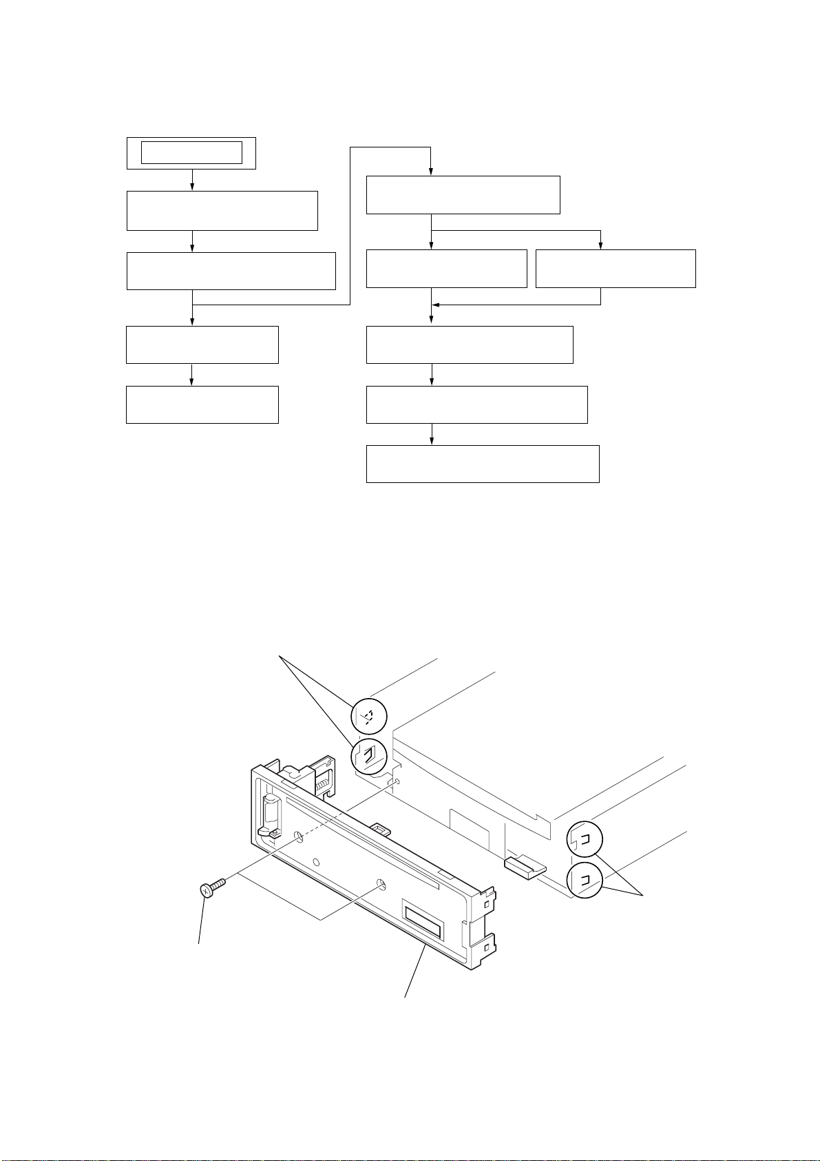
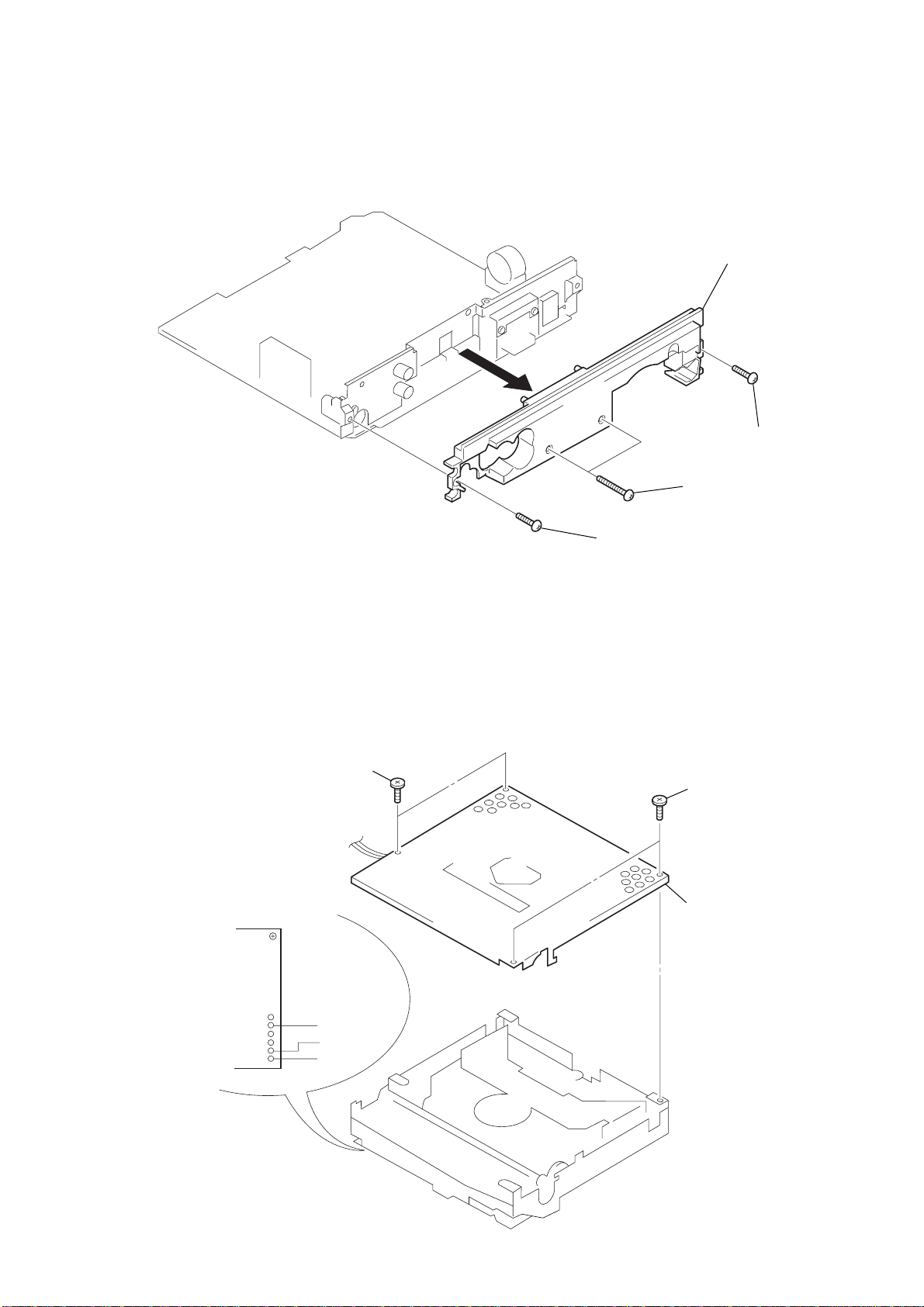
1-1. SUB PANEL ASSY
3
claws
1-7. SERVO BOARD
(Page 8)
1
two screws
(PTT 2.6x6)
4
sub panel assy
2
claws
5
CDX-L480N
)
)
1-2. CD MECHANISM BLOCK
5
CD mechanism block
2
screw
(PTT 2.6x6)
7
bracket (CD)
6
two screws
(PTT 2.6x4
1-3. MAIN BOARD
4
two screws
(PTT 2.6x6)
(ground point)
5
MAIN board
3
4
CNP301
3
screw
(PTT 2.6x6)
(ground point)
1
screw
(PTT 2.6x6)
1
two screws
(PTT 2.6x6
2
two screws
(PTT 2.6x6)
6
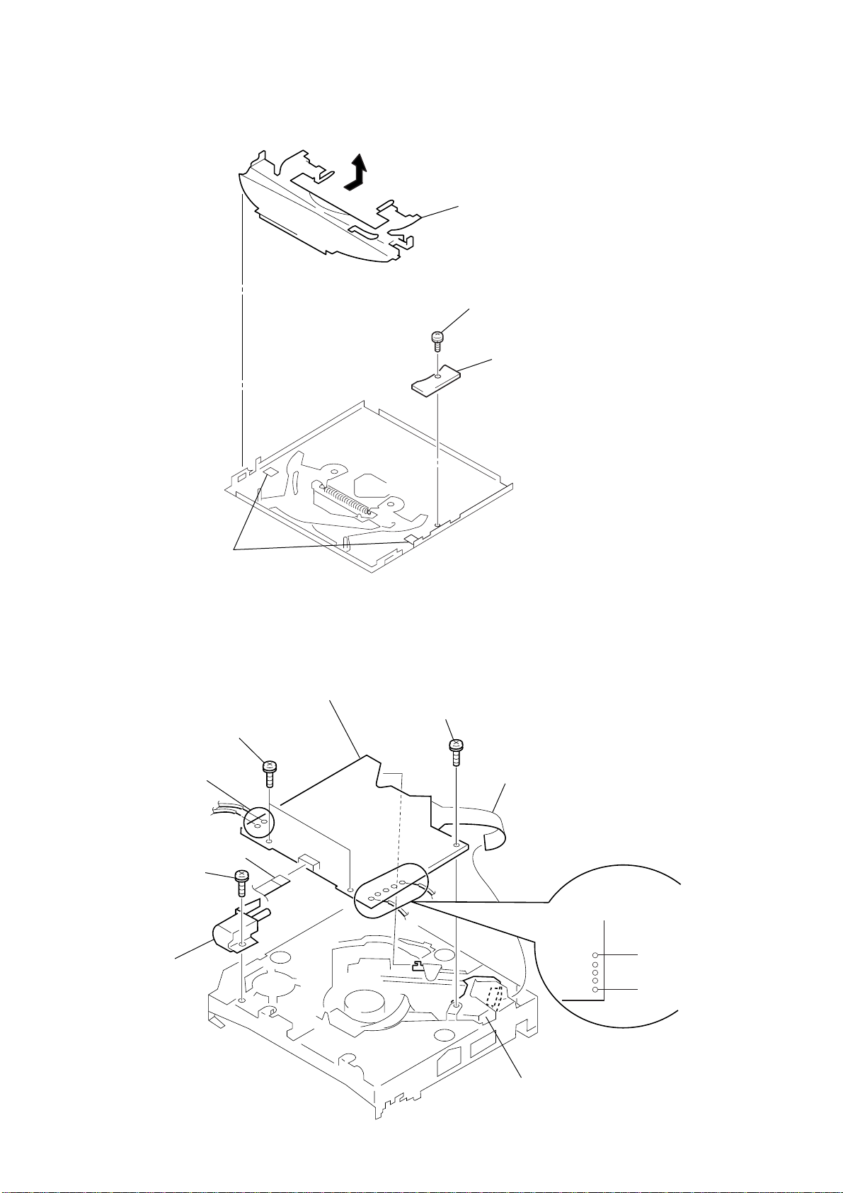
1-4. HEAT SINK
)
4
5
heat sink
3
(PTT 2.6x8
2
two screws
(PTT 2.6x12)
CDX-L480N
screw
1-5. CHASSIS (T.U) ASSY
1
Unsolder the
lead wires.
2
two screws
(P 2x3)
1
screw
(PTT 2.6x8)
3
two screws
(P 2x3)
4
chassis (T.U) assy
black
red
white
7
CDX-L480N
1-6. DISC IN BOARD
4
guide (disc)
1
screw
(PS 2x3)
2
DISC IN board
1-7. SERVO BOARD
2
Removal the solders.
4
(P 2x3)
5
loading motor assy
3
screw
claws
6
(PTT 2x4)
1
CN3
two screws
8
SERVO board
7
screw
(PTT 2x4)
9
PICK-UP FLEXIBLE board
3
Unsolder the
lead wires.
black
yellow
optical pick-up block
8
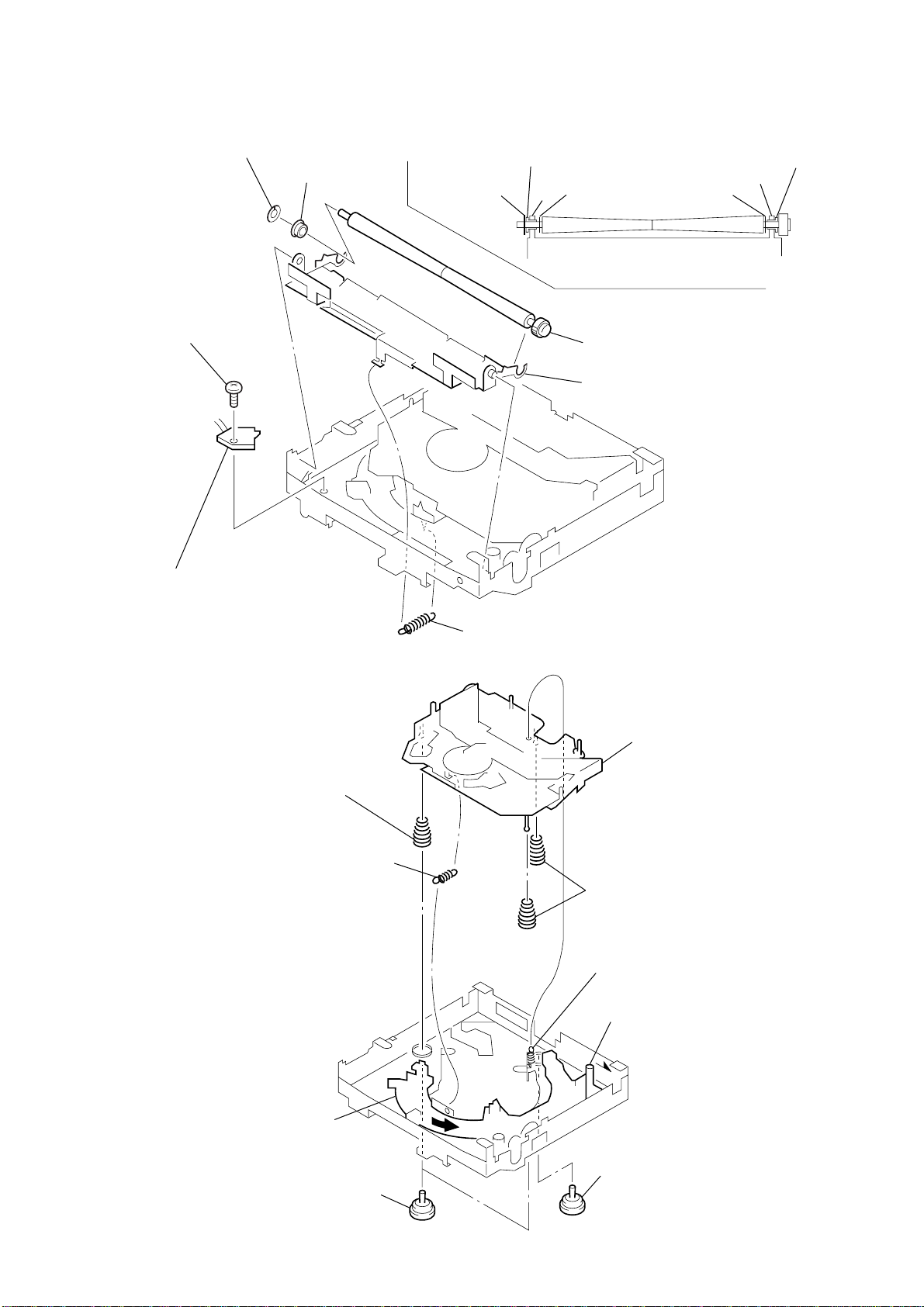
1-8. SHAFT ROLLER ASSY
• When installing, take note of the positions
arm (roller) and washers. (Fig. 1)
3
retaining ring (roller)
4
bearing (roller)
6
screw
(PTT 2x4)
bearing (roller)
retaining ring (roller)
washer (RA)
arm
Fig. 1
5
shaft roller assy
2
arm (roller T)
washer (RA)
CDX-L480N
bearing (roller)
arm
7
LOAD board
1-9. FLOATING BLOCK ASSY
8
compression spring (FL)
1
tension spring (KF1)
1
tension spring (RA3)
7
floating block assy
9
compression spring (FL)
2
tension spring (KR1)
5
Fit lever (D) in the
direction of the arrow.
6
Turn loading ring in the
direction of the arrow.
4
damper (T)
3
damper (T)
9
CDX-L480N
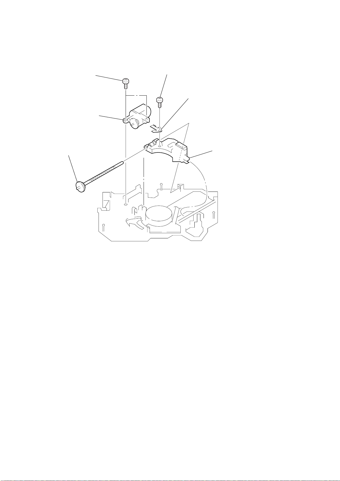
1-10. OPTICAL PICK-UP BLOCK
1
two screws
(P 2x3)
2
sled motor assy
6
shaft (feed) assy
4
screw
(P 2x3)
5
leaf spring (feed)
3
optical pick-up block
10
SECTION 2
DIAGRAMS
2-1. IC PIN DESCRIPTION
• IC501 MN101C49KSG (SYSTEM CONTROL)
Pin No. Pin Name I/O Pin Description
1VREF– — A/D converter power supply (–) pin
2 VSM I S-meter voltage detection input
3QUALITY I Noise detection input
4, 5 KEYIN1, 0 I Key input 1, 0
6 RCIN0 I Rotary commander key input
7 to 9 NIL I Not used. (Fixed at L in this set)
10 VREF+ — A/D converter power supply (+) pin (+5 V)
11 VDD — Power supply pin (+5 V)
12 OSCOUT O Main clock output (18.432 MHz)
13 OSCIN I Main clock input (18.432 MHz)
14 VSS — Ground
15 XIN I Sub clock input (32.768 kHz)
16 XOUT O Sub clock output (32.768 kHz)
17 MMOD I Not used. (Fixed at L in this set)
18 LCDSO O Serial data output for LCD driver IC.
19 LCDCE O Chip enable output for LCD driver IC.
20 LCDCKO O Serial clock output for LCD driver IC.
21 CD_TSO O Serial data output for CD servo IC.
22 CD_TSI I Serial data input from CD servo IC.
23 CD_TCKO O Serial clock output for CD servo IC.
24 SYSRST O Not used. (Fixed at H in this set)
25 BUSON O Not used. (Fixed at H in this set)
26 KEYACK I Key acknowledge detection input
27 DAVN I RDS data block synchronization detection input
28 BUIN I Backup power supply input
29 SIRCS I SIRCS input
30 TU_ATTIN I Tuner attenuator control input
31 CD_PACK I CD text pack synchronization signal input from CD servo IC.
32 NC (VCC) — Power supply pin (+5 V)
33 RESET I Microcomputer reset input
34 NOSE-SW I Not used. (Fixed at H in this set)
35 BEEP O Beep output
36 NC O Not used. (Open)
37 TESTIN I Test mode detection input
38 ACCIN I Accessory power supply detection input
39 NC O Not used. (Open)
40 TELATT I Telephone attenuator detection input
41 NC (VCC) I Not used. (Fixed at H in this set)
42 UNISO O Not used. (Open)
43 UNISI I Not used. (Fixed at L in this set)
44 UNICKO O Not used. (Fixed at L in this set)
45 I2C_SIO I/O I2C BUS serial data input/output
46 NC O Not used. (Open)
47 I2C_CKO O I2C BUS serial clock output
48, 49 NC O Not used. (Open)
50 CD_SELFSW I CD mechanism deck Self switch detection input
51 TSTB O CD text parameter strobe output for CD servo IC.
52 RFOK I RFOK signal input from CD servo IC.
53 CD_RST O Reset signal output for CD servo IC.
54 A0 O Command/parameter discrimination signal output for CD servo IC.
55 STB O Data strobe signal output for CD servo IC.
CDX-L480N
11
CDX-L480N
Pin No. Pin Name I/O Pin Description
56 X_EN O Not used. (Open)
57 LIMIT I CD mechanism deck Limit switch detection input
58 NCO O Not used. (Open)
59 D_SW I CD mechanism deck Down switch detection input
60 INSW I CD mechanism deck Disc in switch detection input
61 NC O Not used. (Open)
62 CD_LM_LO O CD mechanism deck loading motor control output (Loading direction)
63 CD_LM_EJ O CD mechanism deck loading motor control output (Eject direction)
64 to 66 NC O Not used. (Open)
67 ATT O System attenuator control output
68 DIAG I Mode input from power amp IC.
69 STB O Standby control output for power amp IC.
70 VOLATT O Electronic volume attenuator control output
71 to 74 NC O Not used. (Open)
75 DOOR-IND O Not used. (Open)
76 to 84 NC O Not used. (Open)
85 NS_MASK O Noise mask output
86 E2P_CKO O EEPROM serial clock output
87 E2P_SIO I/O EEPROM serial data input/output
88 TU-ATT O Tuner attenuator control output
89, 90 NC O Not used. (Open)
91 AD_ON O Key power supply control output
92, 93 NC O Not used. (Open)
94 PANEL_SW I Front panel OPEN/CLOSE detection input
95 DAVSS — D/A converter power supply (–) pin
96 COLSW I Not used. (Open)
97 FLASH_W I Flash microcomputer write detection input
98 RCIN1 I Rotary commander SHIFT key input
99 NC O Not used. (Open)
100 DAVDD — D/A converter power supply (+) pin (+5 V)
12
 Loading...