

SONY CDX-L470 Service Manual
CDX-L350/L450X/L470X
SERVICE MANUAL
Ver 1.1 2001. 08
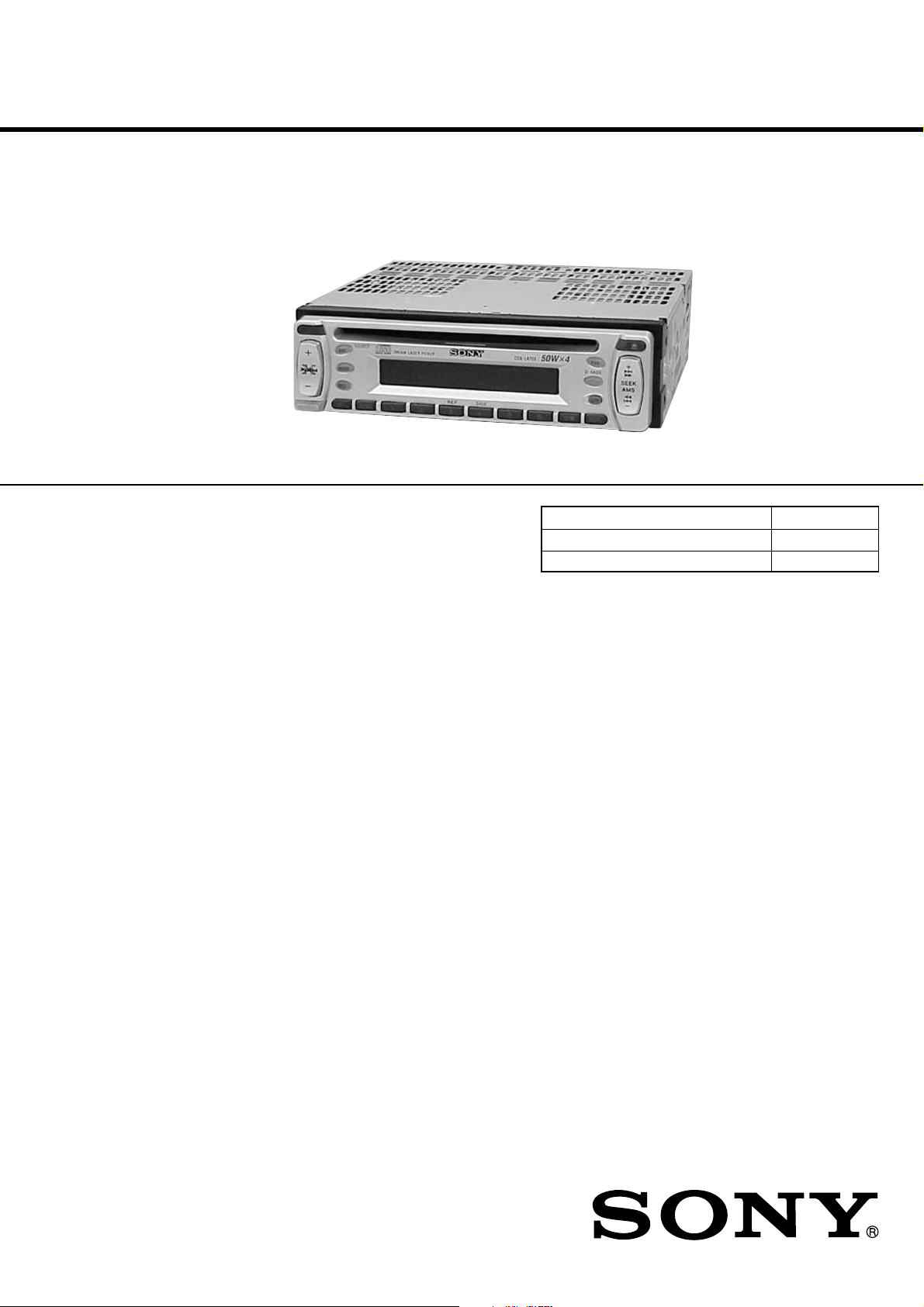
Photo: CDX-L470X
• The CD sections have no adjustments.
SPECIFICATIONS
AUDIO POWER SPECIFICATIONS (US Model)
POWER OUTPUT AND TOTAL HARMONIC DISTORTION
23 watts per channel minimum continuous average power into
4 ohms, 4 channels driven from 20 Hz to 20 kHz with no more
than 5% total harmonic distortion.
CD player section
Signal-to-noise ratio 90 dB
Frequency response 10 – 20,000 Hz
Wow and flutter Below measurable limit
Laser Diode Properties (CDX-L350)
Material GaAlAs
Wavelength 780 nm
Emission Duration Continuous
Laser output power Less than 44.6 µW*
* This output is the value measured at a distance
of 200 mm from the objective lens surface on the
Optical Pick-up Block.
Tuner section
FM
Tuning range CDX-L350:
Antenna terminal External antenna connector
Intermediate frequency 10.7 MHz
Usable sensitivity 11 dBf
Selectivity 75 dB at 400 kHz
Signal-to-noise ratio 65 dB (stereo),
87.5 – 107.9 MHz
CDX-L450X/L470X:
FM tuning interval:
50 kHz/200 kHz
switchable
87.5 – 108 MHz
(at 50 kHz step)
87.5 – 107.9 MHz
(at 200 kHz step)
68 dB (mono)
US Model
Canadian Model
CDX-L350
AEP Model
CDX-L450X
E Model
CDX-L450X/L470X
Model Name Using Similar Mechanism NEW
CD Drive Mechanism Type MG-393X-121//K
Optical Pick-up Name KSS-720A
Harmonic distortion at 1 kHz
0.7% (stereo),
0.5% (mono)
Separation 33 dB at 1 kHz
Frequency response 30 – 15,000 Hz
AM
Tuning range CDX-L350:
530 – 1,710 kHz
CDX-L450X/L470X:
AM tuning interval:
9 kHz/10 kHz
switchable
531 – 1,602 kHz
(at 9 kHz step)
530 – 1,710 kHz
(at 10 kHz step)
Antenna terminal External antenna connector
Intermediate frequency 10.7 MHz/450 kHz
Sensitivity 30 µV
Power amplifier section
Outputs Speaker outputs
(sure seal connectors)
Speaker impedance 4 – 8 ohms
Maximum power output 50 W × 4 (at 4 ohms)
– Continued on next page –
9-870-257-12
2001H0400-1
© 2001. 8
FM/AM COMPACT DISC PLAYER
Sony Corporation
e Vehicle Company
Shinagawa Tec Service Manual Production Group
1
k
CDX-L350/L450X/L470X
General
Outputs Audio output
Power amplifier control
lead (CDX-L350)
Power antenna relay
control lead (CDX-L350)
Power aerial relay control
lead (CDX-L450X/L470X)
Tone controls Bass ±10 dB at 20 Hz (CDX-L350)
Treble ±10 dB at 20 kHz (CDX-L350)
Bass ±9 dB at 100 Hz (L450X/L470X)
Treble ±9 dB at 10 kHz (L450X/L470X)
Power requirements 12 V DC car battery
(negative ground)
Dimensions Approx. 178 × 50 × 176 mm
(7 1/8 × 2 × 7 in.)
(w/h/d)
Mounting dimensions Approx. 182 × 53 × 161 mm
(7 1/4 × 2 1/8 × 6 3/8 in.)
(w/h/d)
Mass Approx. 1.2 kg (2 lb. 10 oz.)
Supplied accessories Parts for installation and
connections (1 set)
Front panel case (1)
Card remote commander
RM-X115 (CDX-L350/L470X)
Note (L450X/L470X)
This unit cannot be connected to a digital
preamplifier or an equalizer.
Design and specifications are subject to change without
notice.
US/Canadian/E model:
CAUTION
Use of controls or adjustments or performance of procedures
other than those specified herein may result in hazardous
radiation exposure.
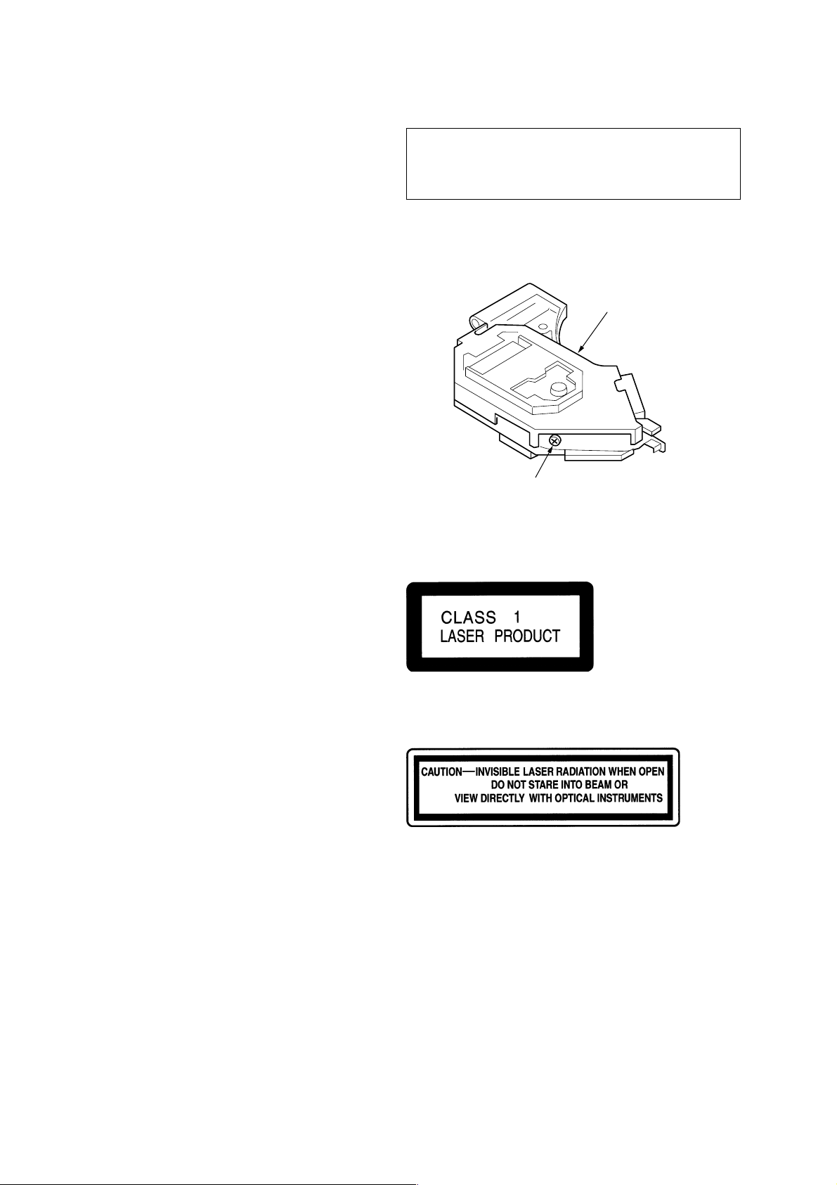
If the optical pick-up block is defective, please replace the whole
optical pick-up block.
Never turn the semi-fixed resistor located at the side of optical
pick-up block.
optical pick-up bloc
semi-fixed resistor
SERVICE NOTES
NOTES ON HANDLING THE OPTICAL PICK-UP BLOCK
OR BASE UNIT
The laser diode in the optical pick-up block may suffer electrostatic
breakdown because of the potential difference generated by the
charged electrostatic load, etc. on clothing and the human body.
During repair, pay attention to electrostatic breakdown and also use
the procedure in the printed matter which is included in the repair
parts.
The flexible board is easily damaged and should be handled with
care.
NOTES ON LASER DIODE EMISSION CHECK
The laser beam on this model is concentrated so as to be focused on
the disc reflective surface by the objective lens in the optical pickup block. Therefore, when checking the laser diode emission, observe from more than 30 cm away from the objective lens.
Notes on Chip Component Replacement
• Never reuse a disconnected chip component.
• Notice that the minus side of a tantalum capacitor may be dam-
aged by heat.
AEP model:
This product is classified as a CLASS 1 LASER PRODUCT.
This label is located on the bottom of the
chassis.
This label is located on the drive unit's internal
chassis.
When replacing the chassis (T) of mechanism deck which have
the “CAUTION LABEL” attached, please be sure to put a new
CAUTION LABEL (3-223-913-11) to the chassis (T).
SAFETY-RELATED COMPONENT WARNING!!
COMPONENTS IDENTIFIED BY MARK 0 OR DOTTED LINE
WITH MARK 0 ON THE SCHEMATIC DIAGRAMS AND IN
THE PARTS LIST ARE CRITICAL TO SAFE OPERATION.
REPLACE THESE COMPONENTS WITH SONY P ARTS WHOSE
PART NUMBERS APPEAR AS SHOWN IN THIS MANUAL OR
IN SUPPLEMENTS PUBLISHED BY SONY.
2
ATTENTION AU COMPOSANT AYANT RAPPORT
À LA SÉCURITÉ!!
LES COMPOSANTS IDENTIFIÉS P AR UNE MARQUE 0 SUR LES
DIAGRAMMES SCHÉMATIQUES ET LA LISTE DES PIÈCES
SONT CRITIQUES POUR LA SÉCURITÉ DE FONCTIONNEMENT.
NE REMPLACER CES COMPOSANTS QUE PAR DES PIÈCES
SONY DONT LES NUMÉROS SONT DONNÉS DANS CE MANUEL
OU DANS LES SUPPLÉMENTS PUBLIÉS PAR SONY.

TABLE OF CONTENTS
1. GENERAL
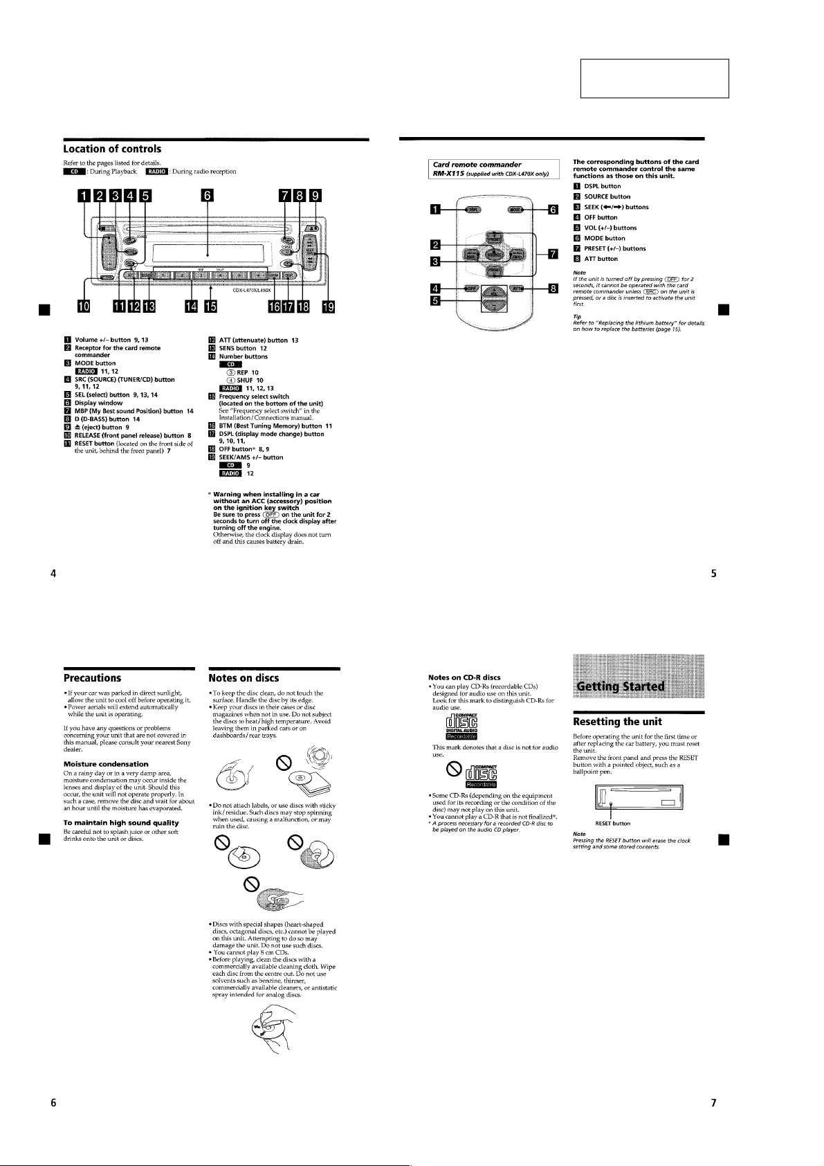
Location of controls................................................................. 4
Getting Started......................................................................... 4
CD Player ................................................................................ 5
Radio ....................................................................................... 5
Other Functions ....................................................................... 6
Connections ............................................................................. 7
2. DISASSEMBLY
2-1. Sub Panel Assy.................................................................... 9
2-2. CD Mechanism Block ....................................................... 10
2-3. Main Board ....................................................................... 10
2-4. Heat Sink ........................................................................... 11
2-5. Chassis (T) Sub Assy ........................................................ 11
2-6. Lever Section .................................................................... 12
2-7. Servo Board....................................................................... 12
2-8. Shaft Roller Assy .............................................................. 13
2-9. Floating Block Assy .......................................................... 13
2-10. Optical Pick-up Block ....................................................... 14
CDX-L350/L450X/L470X
3. ELECTRICAL ADJUSTMENTS.................................15
4. DIAGRAMS
4-1. IC Pin Description............................................................. 17
4-2. Block Diagram –CD Section–........................................... 19
4-3. Block Diagram –Tuner Section–....................................... 20
4-4. Block Diagram –Display Section–.................................... 21
4-5. Circuit Boards Location .................................................... 21
4-6. Printed Wiring Boards –CD Mechanism Section–............ 22
4-7. Schematic Diagram –CD Mechanism Section– ................ 24
4-8. Printed Wiring Board –Main Section–.............................. 25
4-9. Schematic Diagram –Main Section (1/2)– ........................ 26
4-10. Schematic Diagram –Main Section (2/2)– ........................ 27
4-11. Printed Wiring Board –Display Section– .......................... 28
4-12. Schematic Diagram –Display Section–............................. 29
5. EXPLODED VIEWS
5-1. Chassis Section ................................................................. 32
5-2. Front Panel Section ........................................................... 33
5-3. CD Mechanism Section (1) ............................................... 34
5-4. CD Mechanism Section (2) ............................................... 35
5-5. CD Mechanism Section (3) ............................................... 36
6. ELECTRICAL PARTS LIST ........................................ 37
3
CDX-L350/L450X/L470X
SECTION 1
GENERAL
This section is extracted
from instruction manual.
4
CDX-L350/L450X/L470X
5
CDX-L350/L450X/L470X
6
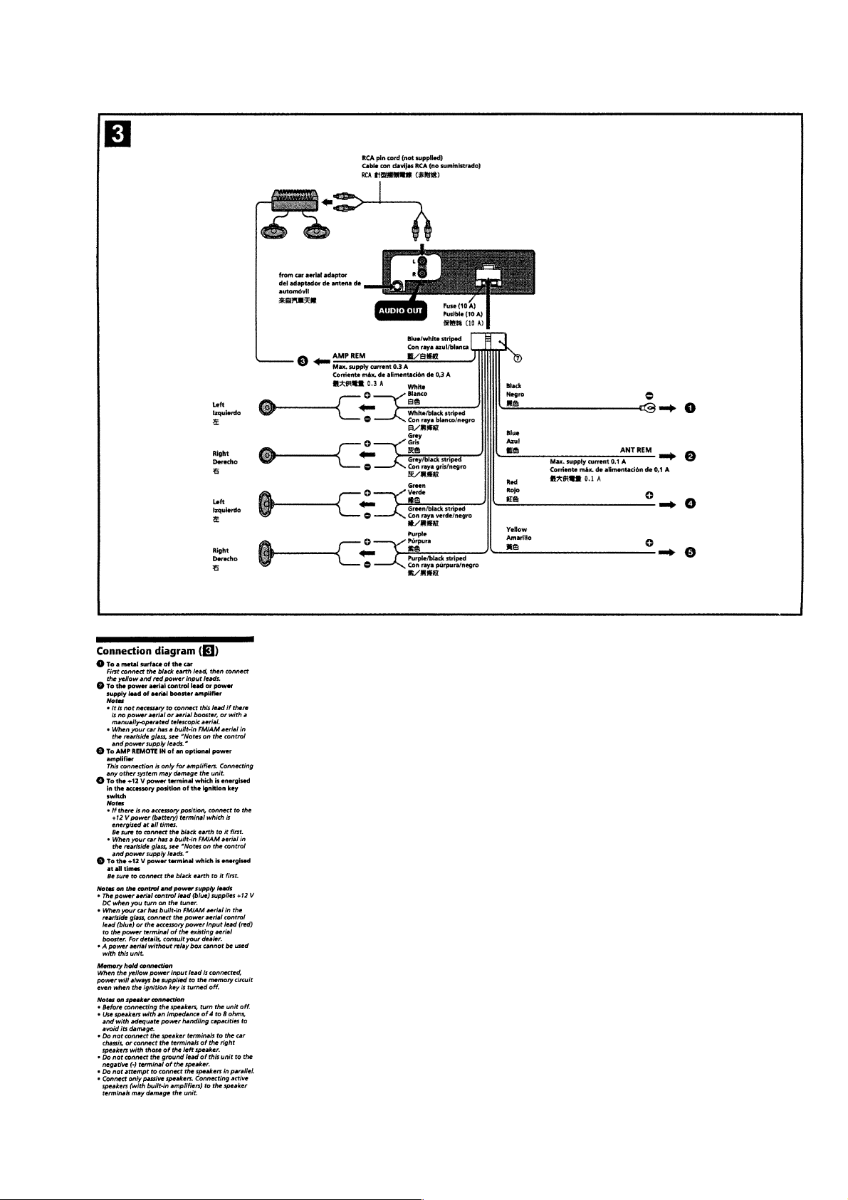
Connections
CDX-L350/L450X/L470X
7
CDX-L350/L450X/L470X
8
SECTION 2
DISASSEMBLY
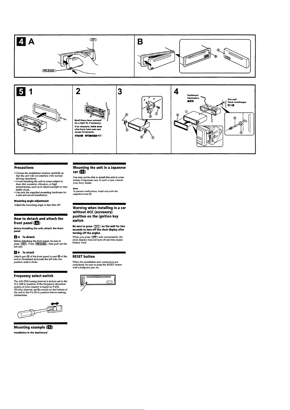
Note : This set can be disassemble according to the following sequence.
CDX-L350/L450X/L470X
Set Sub Panel Assy CD Mechanism Block
Chassis (T) Sub Assy Lever Section
Servo Board
Floating Block Assy Optical Pick-up Block
Note : Follow the disassembly procedure in the numerical order given.
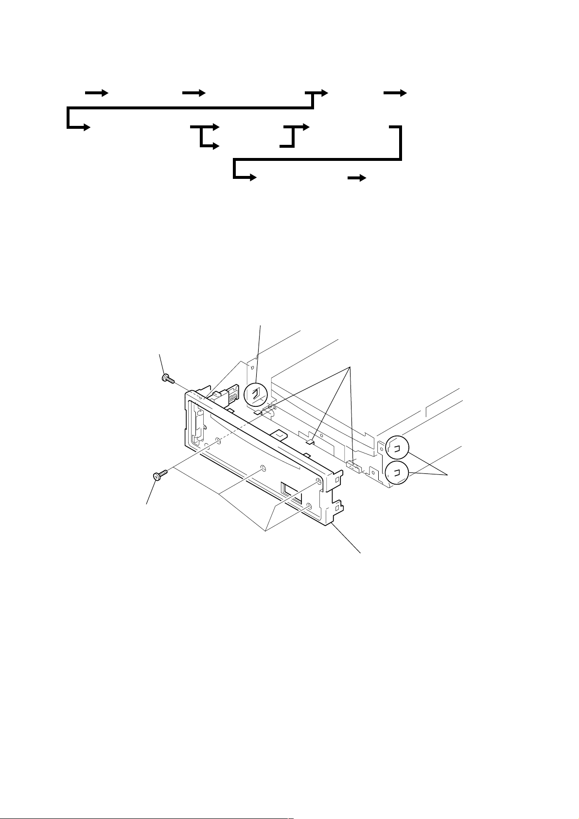
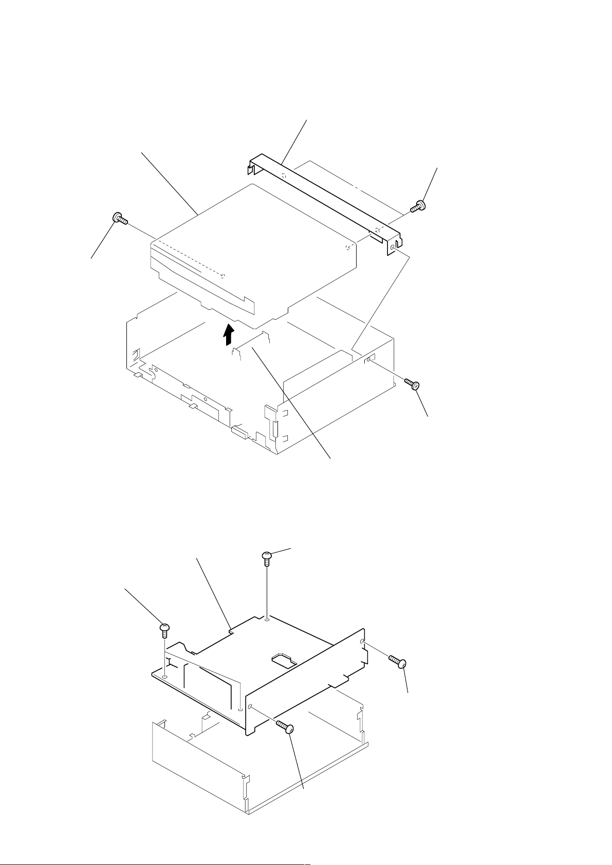
2-1. SUB PANEL ASSY
3 claw
2 PTT 2.6x6
Main Board Heat Sink
Shaft Roller Assy
three claws
1 PTT 2.6x6
4 claws
5 sub panel assy
9
CDX-L350/L450X/L470X
8
6
2-2. CD MECHANISM BLOCK
5 CD mechanism block
2 PTT 2.6x6
7 bracket (CD)
6 PTT 2.6x
2-3. MAIN BOARD
4 screws (+BTT)
3
5 MAIN board
1 PTT 2.6x6
4 CNP701
3 screw (+BTT)
10
2 PTT 2.6x
1 PTT 2.6x8
6 heat sink
1 PTT 2.6x8
2 PTT 2.6x8
4 PTT 2.6x8
3 PTT 2.6x12
5 PTT 2.6x8
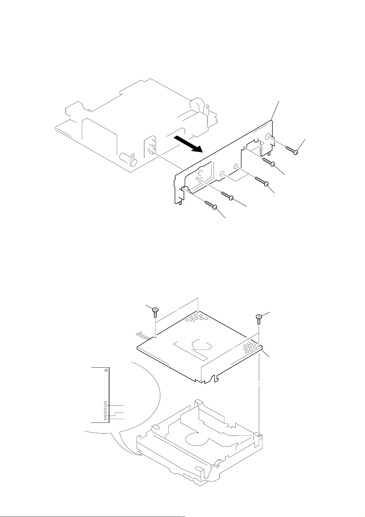
2-4. HEAT SINK
CDX-L350/L450X/L470X
2-5. CHASSIS (T) SUB ASSY
1 Unsolder the
lead wires.
2 P 2x3
3 P 2x3
4 chassis (T) sub assy
black
red
white
11
CDX-L350/L450X/L470X
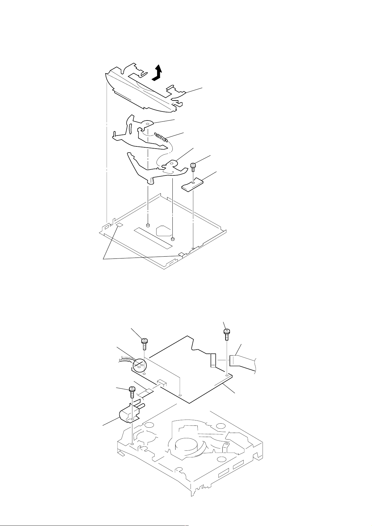
2-6. LEVER SECTION
5 guide (disc)
6 lever (R)
3 tension spring (LR)
7 lever (L)
1 special screw
2 IN SELF SW board
2-7. SERVO BOARD
4 claws
6 special screws
3 Removal the solders.
1 CN3
4 P 2x3
5 loading motor assy
7 special screw
2 CN2
8 SERVO board
12
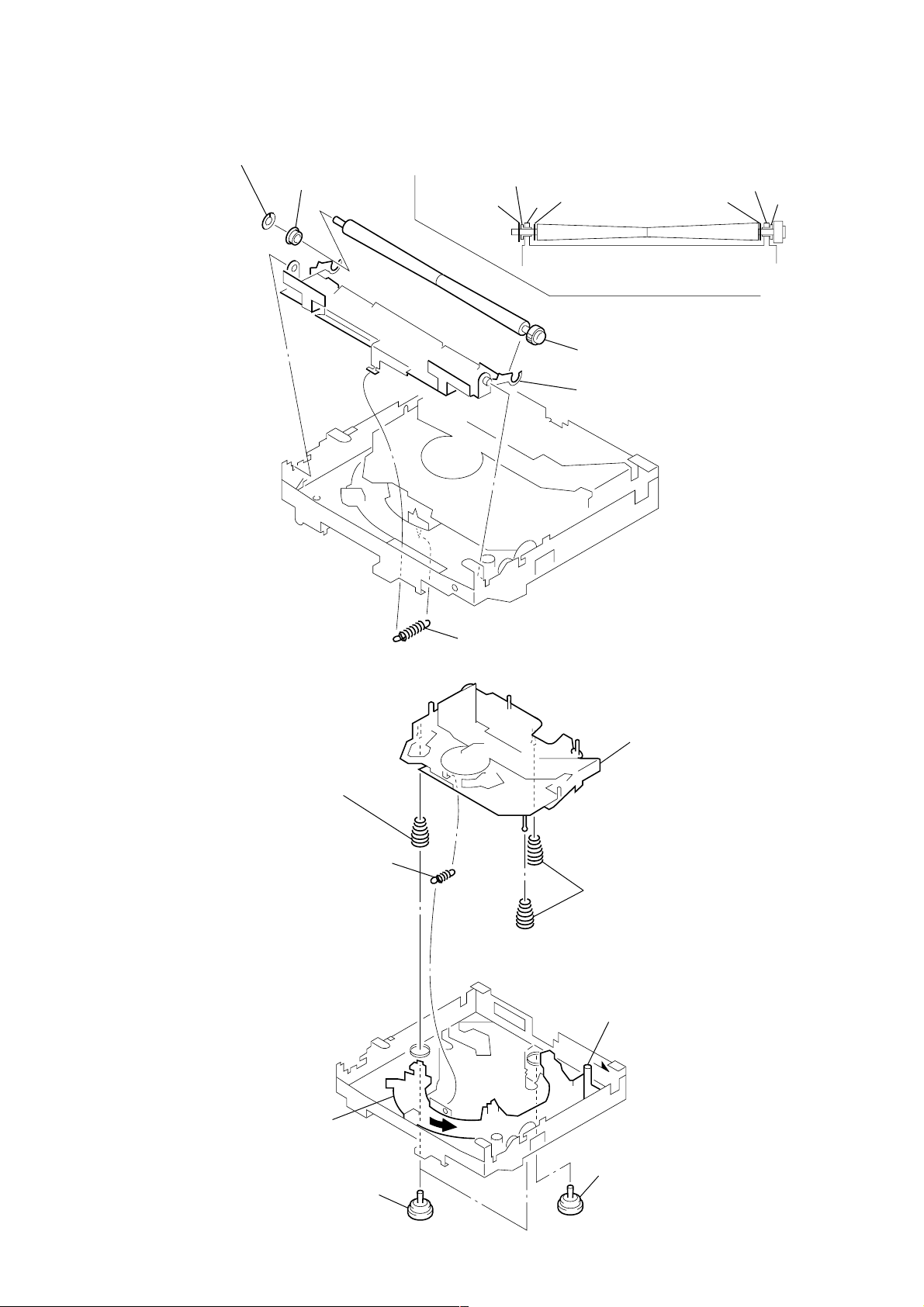
Fig. 1
1 tension spring (RA)
2 arm (roller)
3 retaing ring (RA)
4 shaft retainer
5 shaft roller assy
retaing ring (RA)
arm
arm
washer
washer
shaft retainer
shaft retainer
2-8. SHAFT ROLLER ASSY
• When installing, take note of the positions
arm (roller) and washers. (Fig. 1)
CDX-L350/L450X/L470X
2-9. FLOATING BLOCK ASSY
7 compression spring (FL)
1 tension spring (KF1)
5 Turn loading ring in the
direction of the arrow.
6 floating block assy
8 compression spring (FL)
4 Fit lever (D) in the
direction of the arrow.
3 damper (T)
2 damper (T)
13
CDX-L350/L450X/L470X
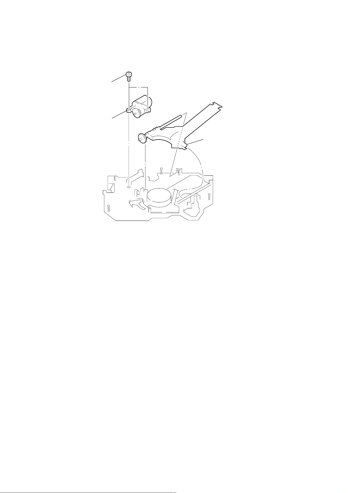
2-10. OPTICAL PICK-UP BLOCK
1 P 2x3
2 sled motor assy
3 optical pick-up block
14
SECTION 3
ELECTRICAL ADJUSTMENTS
CDX-L350/L450X/L470X
TEST MODE
This set have the test mode function. In the test mode, FM Auto
Scan/Stop Level and AM Auto Scan/Stop Level check can be
performed easier than it in ordinary procedure.
<Set the Test Mode>
1. Turn ON the regulated power supply to ACC and BATT
terminals is “OFF” position (display 1:00).
2. Push the preset 4 button.
3. Push the preset 5 button.
4. Press the preset 1 button for more than two seconds.
5. Then the display and LED on the front panel indicates all lights,
the test mode is set.
<Release the Test Mode>
1. Push the OFF button.
TUNER SECTION
Cautions during repair
When the tuner unit is defective, replace it by a new one because
its internal block is difficult to repair.
Note on Adjustment
The adjustments of tuner section, should be performed according
to the following sequence.
1. FM Auto Scan/Stop Level Adjustment
2. FM Stereo Separation Adjustment
3. AM Auto Scan/Stop Level Adjustment
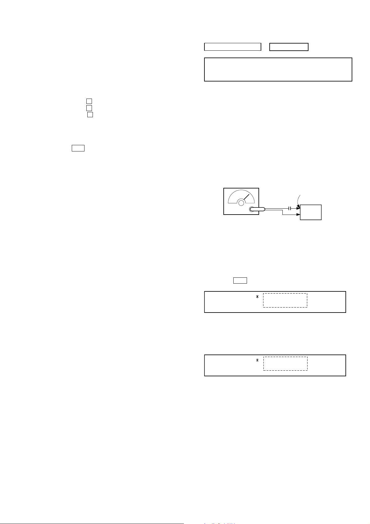
FM Auto Scan/Stop Level Adjustment
Setting :
SOURCE button : FM
FREQUENCY SELECT switch (L450X/L470X): FM 50k
FM RF signal
generator
Carrier frequency : 97.9 MHz (L350)
Output level : 22 dB (12.6 µV)
Mode : mono
Modulation : 1 kHz, 22.5 kHz deviation (30%)
0 dB = 1 µV
antenna
0.01 µF
: 98.0 MHz (L450X/L470X)
terminal
set
Procedure :
1. Set to the test mode.
2. Push the SRC button and set to FM.
Display
1
FM
ST
3. Adjust with the volume RV2 on TU601 so that the “FM”
indication turns to “FM0” indication on the display window.
But, in case of already indicated “FM0”, turn the RV2 so that
put out light “0” indication and adjustment.
FM0Z
*1: L450X/L470X are indicates “98.00”.
Adjustment Location : See page 16.
ST
97.90
l
Display
1
97.90
l
Z
SHUF
Z
SHUF
15
CDX-L350/L450X/L470X
r
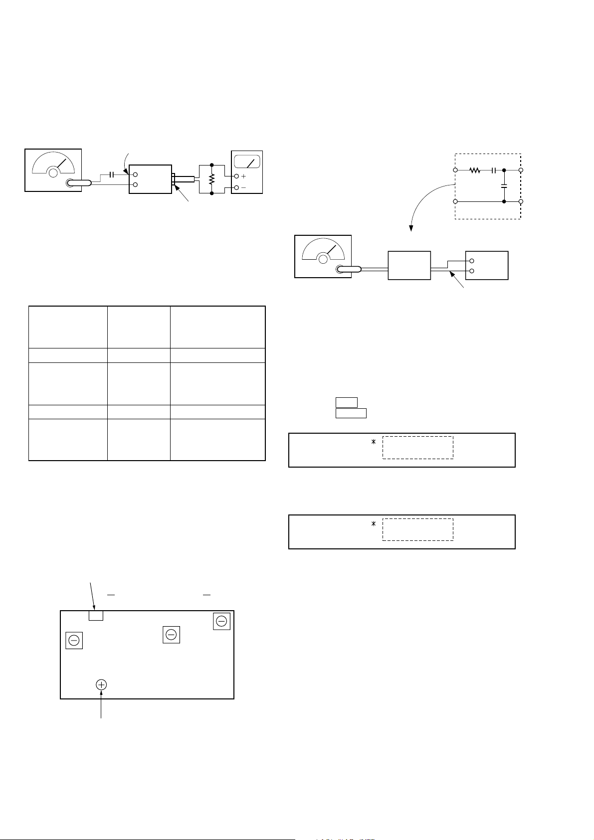
FM Stereo Separation Adjustment
Setting :
SOURCE button : FM
FREQUENCY SELECT switch (L450X/L470X): FM 50k
FM RF signal
generator
0.01 µF
Carrier frequency : 97.9 MHz (L350)
: 98.0 MHz (L450X/L470X)
Output level : 70 dB (3.2 mV)
Mode : stereo
Modulation : main :1 kHz, 33.75 kHz deviation (45%)
sub :1 kHz, 33.75 kHz deviation (45%)
19 kHz pilot : 7.5 kHz deviation (10%)
Procedure :
FM stereo
signal generator
output channel
L-CH L-CH A
R-CH L-CH Adjust RV1 on TU601
R-CH R-CH C
L-CH R-CH Adjust RV1 on TU601
L-CH stereo separation : A – B
R-CH stereo separation : C – D
The separations of both channels should be equal.
Specification : Separation more than 24 dB
Adjustment Location :
RV2
FM Auto Scan/Stop
Level Adjustment
antenna
terminal
set
AUDIO OUT REAR
Level meter Level meter
connection reading (dB)
for maximum reading.
for maximum reading.
level mete
10 kΩ
B
D
AM Auto Scan/Stop Level Check
Note : This adjustment should be performed after the FM Auto
Scan / Stop Level Adjustment is done.
Setting :
SOURCE t MODE button : AM
FREQUENCY SELECT switch (L450X/L470X): AM 9k
15 pF
30 Ω
65 pF
AM RF signal
generator
Carrier frequency : 1000 kHz (L350)
Output level : 30 dB (44.7 µV)
Mode : mono
Modulation : 1 kHz, 22.5 kHz deviation (30%)
Procedure :
1. Set to the test mode. (See page 15)
2. Push the SRC button.
3. Push the MODE button and set to AM.
AM
ST
4. Check that the “AM” indication turns to “AM0” indication on
the display window.
AM0Z
ST
*2: L450X/L470X are indicates “999”.
AM dummy
antenna (50 Ω)
: 999 kHz (L450X/L470X)
Display
2
1 00ZZZ
Display
2
1 00ZZZ
0
SHUF
0
SHUF
set
set
antenna
terminal
16
TU601(Component Side)
RV1
FM Stereo Separation
Adjustment
SECTION 4
DIAGRAMS
4-1. IC PIN DESCRIPTION
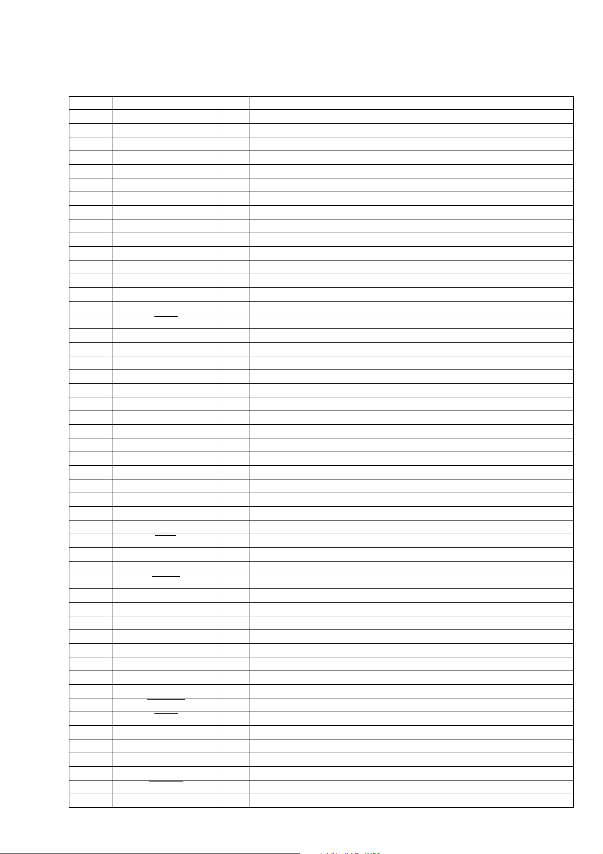
• IC801 µPD780024AGK-B26-9ET (SYSTEM CONTROLLER)
Pin No. Pin Name I/O Pin Description
1 D SW I Down switch detection input
2 IN SW I Disc in switch detection input
3 PH3 I PH3 detection input (Not used in this set)
4 LM LD O Loading motor drive output (Loading)
5 LM EJ O Loading motor drive output (Eject)
6 A ATT O Power amplifier mute control output
7 ATT O Line out mute control output
8 BEEP O BEEP output
9 VSSO — Ground
10 VDDO — Power supply pin (+5 V)
11 VOL CLK O Electric volume clock output
12 VOL DO O Electric volume data out output
13 VOL CE O Electric volume chip enable output
14 AM ON O Tuner AM power supply control output
15 FM ON O Tuner FM power supply control output
16 NOSE I Front panel attachment detection input
17 PLL DI I PLL IC data input
18 LCD DO O LCD data output
19 LCD CE O LCD chip enable output
20 LCD CLK O LCD clock output
21 PLL CLK O PLL IC clock output
22 PLL DO O PLL IC data output
23 PLL CE O PLL IC chip enable output
24 VDD1 — Power supply pin (+5 V)
25 AVSS — Ground
26 ST IND I FM STEREO detection input
27 FUN SEL I Function select input
28 S METER I S meter signal input
29, 30 KEY0, 1 I A/D key input 0, 1
31 TEL ATT I Attenuator signal input
32 DST SEL I Destination select input
33 TEST I Force test mode input
34 AVREF — A/D converter power supply pin (+5 V)
35 AVDD — A/D converter power supply pin (+5 V)
36 RESET I Reset input
37 XT2 O Sub clock output (32.768 kHz)
38 XT1 I Sub clock input (32.768 kHz)
39 IC — Connect to Ground in this set.
40 X2 O Master clock output (8.38 MHz)
41 X1 I Master clock input (8.38 MHz)
42 VSS1 — Ground
43 KEY ACK I Key acknowledge detection input
44 SIRCS I SIRCS input
45 SELF SW I Self switch detection input
46 BU IN I Backup power supply detection input
47 AD ON O Key power supply control output
48 ILL ON O Illumination power supply control output
49 AMP ON O Amplifier remote power supply control output
50 CDM ON O CD mechanism deck power supply control output
51 XCD ON O CD DSP IC 16 MHz X’tal ON/OFF control output
52 TU ON O Tuner power supply control output
CDX-L350/L450X/L470X
17
 Loading...