

Page 1
CDX-L300/L460X
SERVICE MANUAL
Ver 1.3 2003. 08
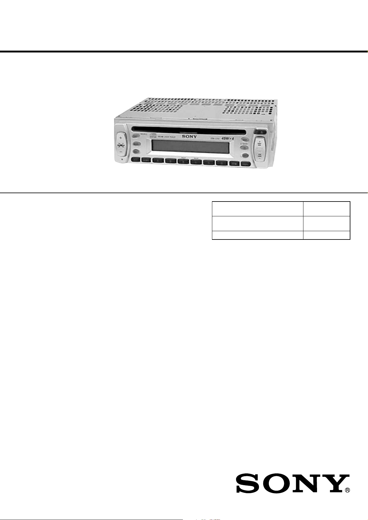
Photo: CDX-L460X
• The CD sections have no adjustments.
SPECIFICATIONS
US Model
Canadian Model
CDX-L300
E Model
CDX-L460X
Model Name Using Similar Mechanism
CD Drive Mechanism Type
Optical Pick-up Name KSS-720A
CDX-L250/L430X
NEW
MG-393X-121//K
MG-393XA-121//K
AUDIO POWER SPECIFICATIONS (US Model)
POWER OUTPUT AND TOTAL HARMONIC DISTORTION
22 watts per channel minimum continuous average power into
4 ohms, 4 channels driven from 20 Hz to 20 kHz with no more
than 5% total harmonic distortion.
CD player section
Signal-to-noise ratio 90 dB
Frequency response 10 – 20,000 Hz
Wow and flutter Below measurable limit
Laser Diode Properties (CDX-L300)
Material GaAlAs
Wavelength 780 nm
Emission Duration Continuous
Laser output power Less than 44.6 µW*
* This output is the value measured at a distance
of 200 mm from the objective lens surface on the
Optical Pick-up Block.
Tuner section
FM
Tuning range CDX-L300:
Antenna terminal External antenna connector
Intermediate frequency 10.7 MHz
Usable sensitivity 11 dBf
Selectivity 75 dB at 400 kHz
Signal-to-noise ratio 65 dB (stereo),
87.5 – 107.9 MHz
CDX-L460X:
FM tuning interval:
50 kHz/200 kHz
switchable
87.5 – 108 MHz
(at 50 kHz step)
87.5 – 107.9 MHz
(at 200 kHz step)
68 dB (mono)
Harmonic distortion at 1 kHz
0.7% (stereo),
0.5% (mono)
Separation 33 dB at 1 kHz
Frequency response 30 – 15,000 Hz
AM
Tuning range CDX-L300:
530 – 1,710 kHz
CDX-L460X:
AM tuning interval:
9 kHz/10 kHz
switchable
531 – 1,602 kHz
(at 9 kHz step)
530 – 1,710 kHz
(at 10 kHz step)
Antenna terminal External antenna connector
Intermediate frequency 10.7 MHz/450 kHz
Sensitivity 30 µV
Power amplifier section
Outputs Speaker outputs
(sure seal connectors)
Speaker impedance 4 – 8 ohms
Maximum power output 45 W × 4 (at 4 ohms)
– Continued on next page –
FM/AM COMPACT DISC PLAYER
9-873-402-04
2003H04-1
© 2003. 08
Sony Corporation
e Vehicle Company
Published by Sony Engineering Corporation
1
Page 2
k
CDX-L300/L460X
General
Outputs Audio output
Power amplifier control lead
(CDX-L300)
Power antenna relay
control lead (CDX-L300)
Power aerial relay control
lead (CDX-L460X)
Tone controls Bass ±10 dB at 20 Hz (CDX-L300)
Treble ±10 dB at 20 kHz (CDX-L300)
Bass ±9 dB at 100 Hz (CDX-L460X)
Treble ±9 dB at 10 kHz (CDX-L460X)
Power requirements 12 V DC car battery
(negative ground)
Dimensions Approx. 178 × 50 × 176 mm
(7 1/8 × 2 × 7 in.)
(w/h/d)
Mounting dimensions Approx. 182 × 53 × 161 mm
(7 1/4 × 2 1/8 × 6 3/8 in.)
(w/h/d)
Mass Approx. 1.2 kg (2 lb. 10 oz.)
Supplied accessories Parts for installation and
connections (1 set)
Note (CDX-L460X)
This unit cannot be connected to a digital
preamplifier or an equalizer.
Design and specifications are subject to change without
notice.
SERVICE NOTES
CAUTION
Use of controls or adjustments or performance of procedures
other than those specified herein may result in hazardous
radiation exposure.
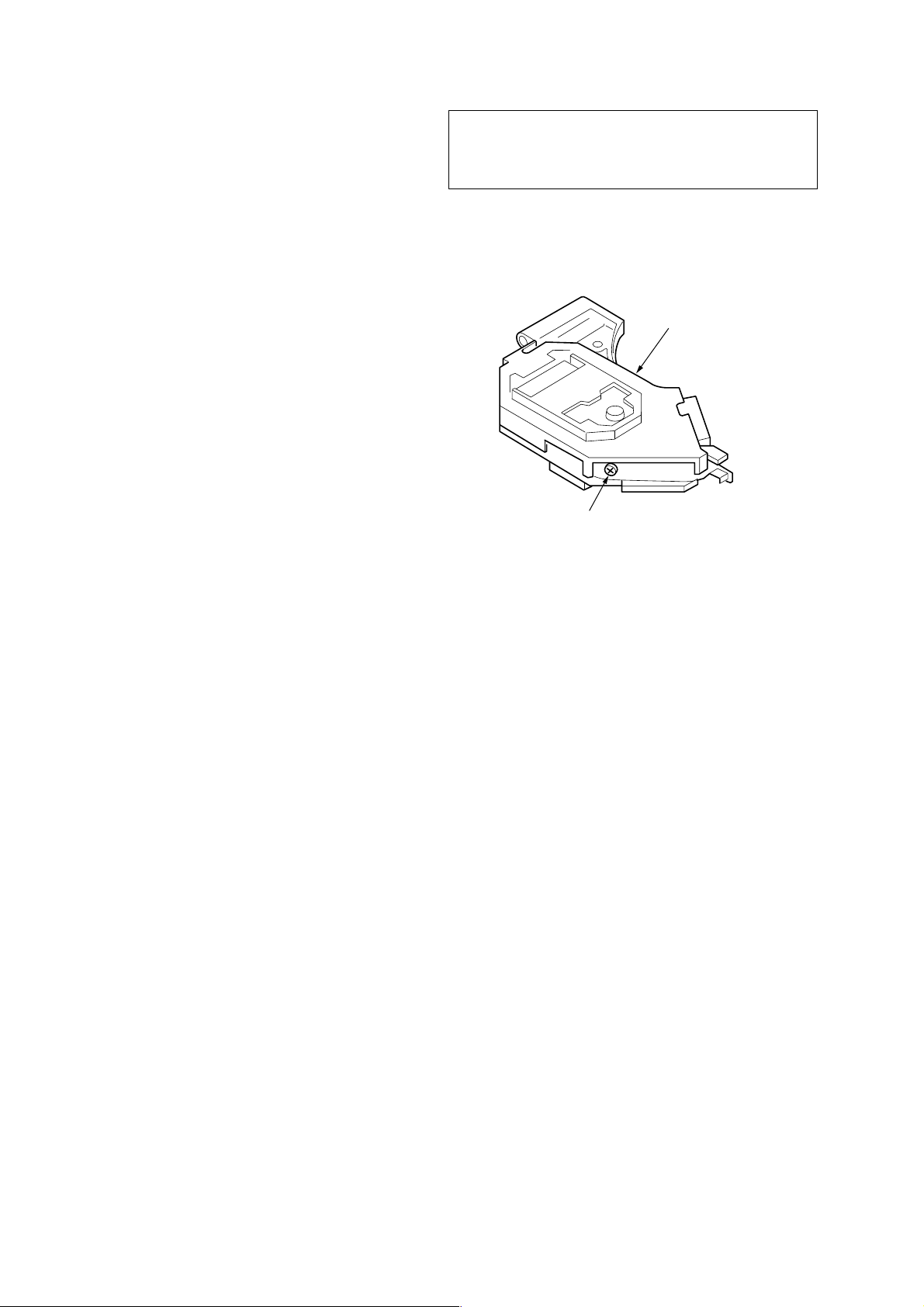
If the optical pick-up block is defective, please replace the whole
optical pick-up block.
Never turn the semi-fixed resistor located at the side of optical
pick-up block.
optical pick-up bloc
semi-fixed resistor
NOTES ON HANDLING THE OPTICAL PICK-UP BLOCK
OR BASE UNIT
The laser diode in the optical pick-up block may suffer electrostatic
breakdown because of the potential difference generated by the
charged electrostatic load, etc. on clothing and the human body.
During repair, pay attention to electrostatic breakdown and also use
the procedure in the printed matter which is included in the repair
parts.
The flexible board is easily damaged and should be handled with
care.
NOTES ON LASER DIODE EMISSION CHECK
The laser beam on this model is concentrated so as to be focused on
the disc reflective surface by the objective lens in the optical pickup block. Therefore, when checking the laser diode emission, observe from more than 30 cm away from the objective lens.
Notes on Chip Component Replacement
• Never reuse a disconnected chip component.
• Notice that the minus side of a tantalum capacitor may be dam-
aged by heat.
SAFETY-RELATED COMPONENT WARNING!!
COMPONENTS IDENTIFIED BY MARK 0 OR DOTTED LINE
WITH MARK 0 ON THE SCHEMATIC DIAGRAMS AND IN
THE PARTS LIST ARE CRITICAL TO SAFE OPERATION.
REPLACE THESE COMPONENTS WITH SONY P ARTS WHOSE
PART NUMBERS APPEAR AS SHOWN IN THIS MANUAL OR
IN SUPPLEMENTS PUBLISHED BY SONY.
ATTENTION AU COMPOSANT AYANT RAPPORT
À LA SÉCURITÉ!!
TEST DISCS
This set can playback CD-R and CD-ROM discs. The following
test discs should be used to check the capability:
CD-R test disc TCD-R082LMT (Part No. J-2501-063-1)
CD-RW test disc TCD-W082L (Part No. J-2501-063-2)
LES COMPOSANTS IDENTIFIÉS P AR UNE MARQUE 0 SUR LES
DIAGRAMMES SCHÉMATIQUES ET LA LISTE DES PIÈCES
SONT CRITIQUES POUR LA SÉCURITÉ DE FONCTIONNEMENT.
NE REMPLACER CES COMPOSANTS QUE PAR DES PIÈCES
SONY DONT LES NUMÉROS SONT DONNÉS DANS CE MANUEL
OU DANS LES SUPPLÉMENTS PUBLIÉS PAR SONY.
2
Page 3
Notes for Inspection of the Mechanism Deck
The CDX-L300 uses two types of mechanism decks.
Former type: MG-393X-121//K
New type: MG-393XA-121//K
The CDX-L460X only uses the MG-393XA-121//K.
When inspecting and/or serving, check the model No. printed on
the SERVO board.
- SERVO BOARD (SIDE A) -
CDX-L300/L460X
MG-393X//K:MG-393X-121//K
MG-393XA//K:MG-393XA-121//K
3
Page 4
CDX-L300/L460X
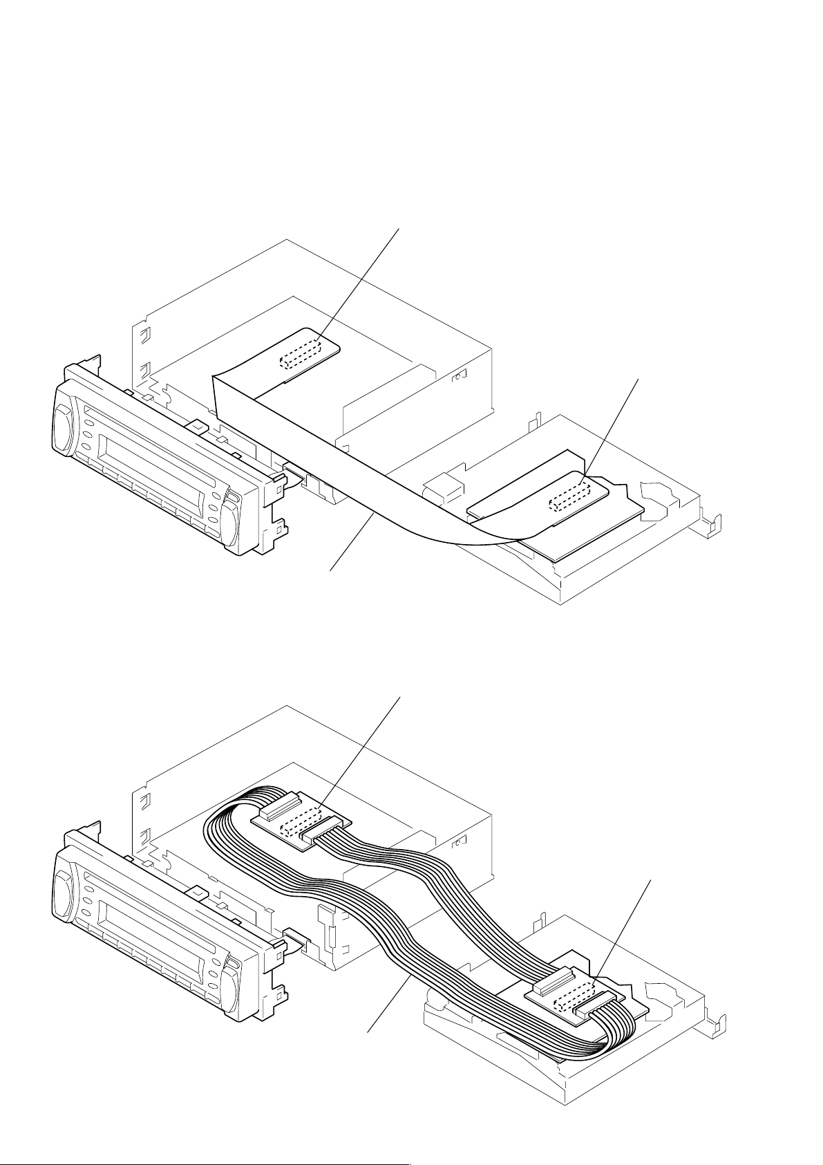
EXTENSION CABLE AND SERVICE POSITION
When repairing or servicing this set, connect the jig (extension cable)
as shown below.
MG-393X-121//K
• Connect the MAIN board (CNP701) and the SERV O board (CN1)
with the extension cable (Part No. J-2502-011-1).
MAIN BOARD CNP701
SERVO BOARD CN1
J-2502-011-1
MG-393XA-121//K
• Connect the MAIN board (CNP701) and the SERV O board (CN1)
with the extension cable (Part No. J-2502-062-1).
MAIN BOARD CNP701
SERVO BOARD CN1
J-2502-062-1
4
Page 5

TABLE OF CONTENTS
CDX-L300/L460X
1. GENERAL
Location of controls (L300) .................................................... 6
Location of controls (L460X).................................................. 6
Getting Started......................................................................... 6
CD Player ................................................................................ 7
Radio ....................................................................................... 7
Other Functions ....................................................................... 8
Additional Information............................................................ 8
Connections (L300) ................................................................. 9
Connections (L460X) ............................................................ 11
2. DISASSEMBLY
2-1. Front Panel Assy ............................................................... 13
2-2. CD Mechanism Block ....................................................... 14
2-3. Main Board ....................................................................... 14
2-4. Heat Sink ........................................................................... 15
2-5. Chassis (T) Sub Assy ........................................................ 15
2-6. Lever Section..................................................................... 16
2-7. Servo Board....................................................................... 16
2-8. Shaft Roller Assy .............................................................. 17
2-9. Floating Block Assy .......................................................... 17
2-10. Optical Pick-up Block ....................................................... 18
3. DIAGRAMS
3-1. IC Pin Description............................................................. 19
3-2. Block Diagram –CD Section–........................................... 21
3-3. Block Diagram –Tuner Section–....................................... 22
3-4. Block Diagram –Display Section–.................................... 23
3-5. Circuit Boards Location .................................................... 24
3-6. Schematic Diagram
–CD Mechanism Section (MG-393X-121//K)– ................ 25
3-7. Printed Wiring Boards
–CD Mechanism Section (MG-393X-121//K)– ................ 26
3-8. Printed Wiring Boards
–CD Mechanism Section (MG-393XA-121//K)– ............. 28
3-9. Schematic Diagram
–CD Mechanism Section (MG-393XA-121//K)– ............. 30
3-10. Printed Wiring Board –Main Section– .............................. 31
3-11. Schematic Diagram –Main Section (1/2)– ........................ 32
3-12. Schematic Diagram –Main Section (2/2)– ........................ 33
3-13. Printed Wiring Board –Display Section– .......................... 34
3-14. Schematic Diagram –Display Section–............................. 35
4. EXPLODED VIEWS
4-1. Chassis Section ................................................................. 38
4-2. Front Panel Section ........................................................... 39
4-3. CD Mechanism Section (1) (MG-393X-121//K) .............. 40
4-4. CD Mechanism Section (2) (MG-393X-121//K) .............. 41
4-5. CD Mechanism Section (3) (MG-393X-121//K) .............. 42
4-6. CD Mechanism Section (1) (MG-393XA-121//K) ........... 43
4-7. CD Mechanism Section (2) (MG-393XA-121//K) ........... 44
4-8. CD Mechanism Section (3) (MG-393XA-121//K) ........... 45
5. ELECTRICAL PARTS LIST ........................................ 46
5
Page 6
CDX-L300/L460X
(L300) (L460X)
SECTION 1
GENERAL
This section is extracted
from instruction manual.
6
Page 7
CDX-L300/L460X
7
Page 8
CDX-L300/L460X
8
Page 9
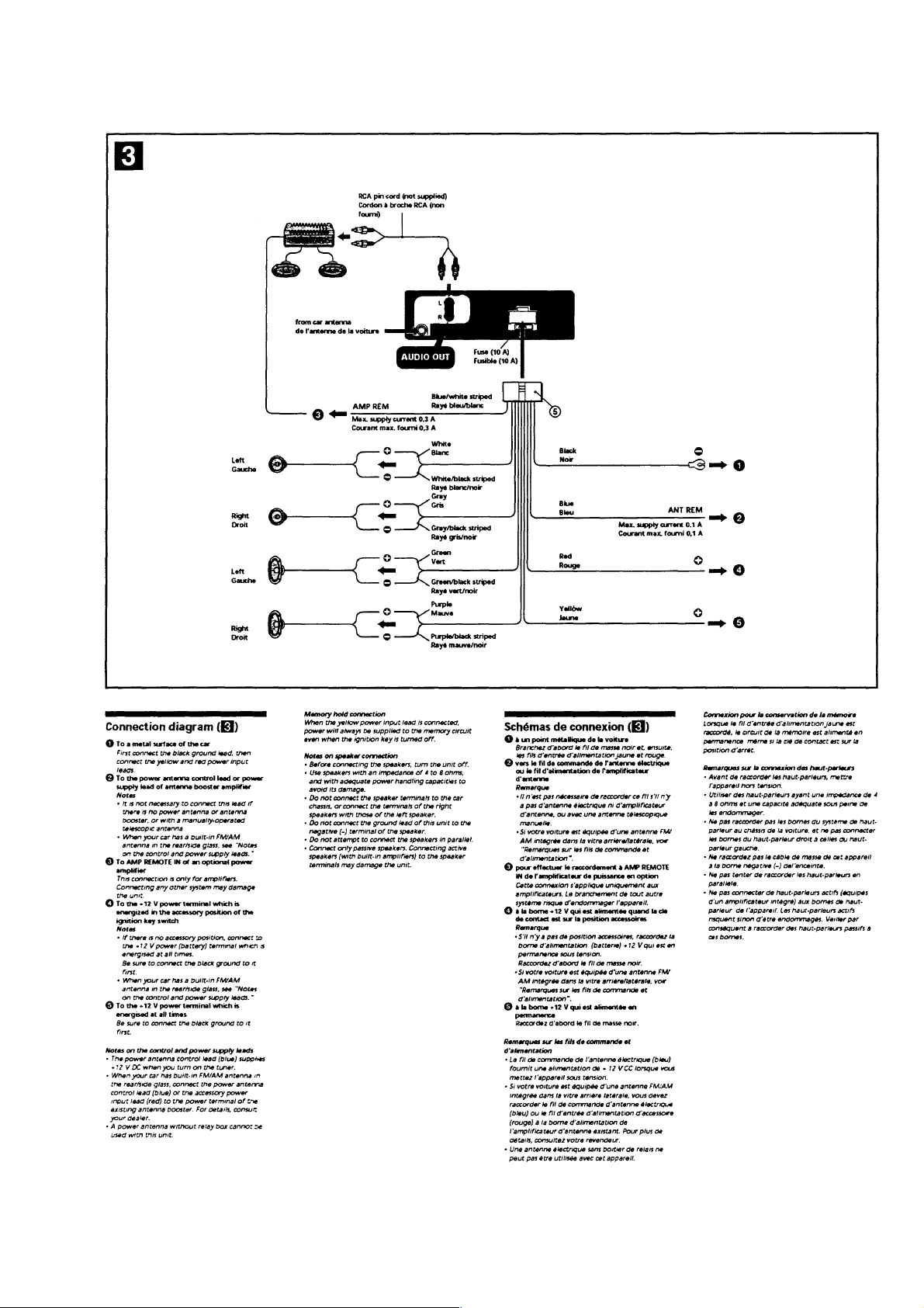
• Connections (L300)
CDX-L300/L460X
9
Page 10
CDX-L300/L460X
10
Page 11
• Connections (L460X)
CDX-L300/L460X
11
Page 12
CDX-L300/L460X
12
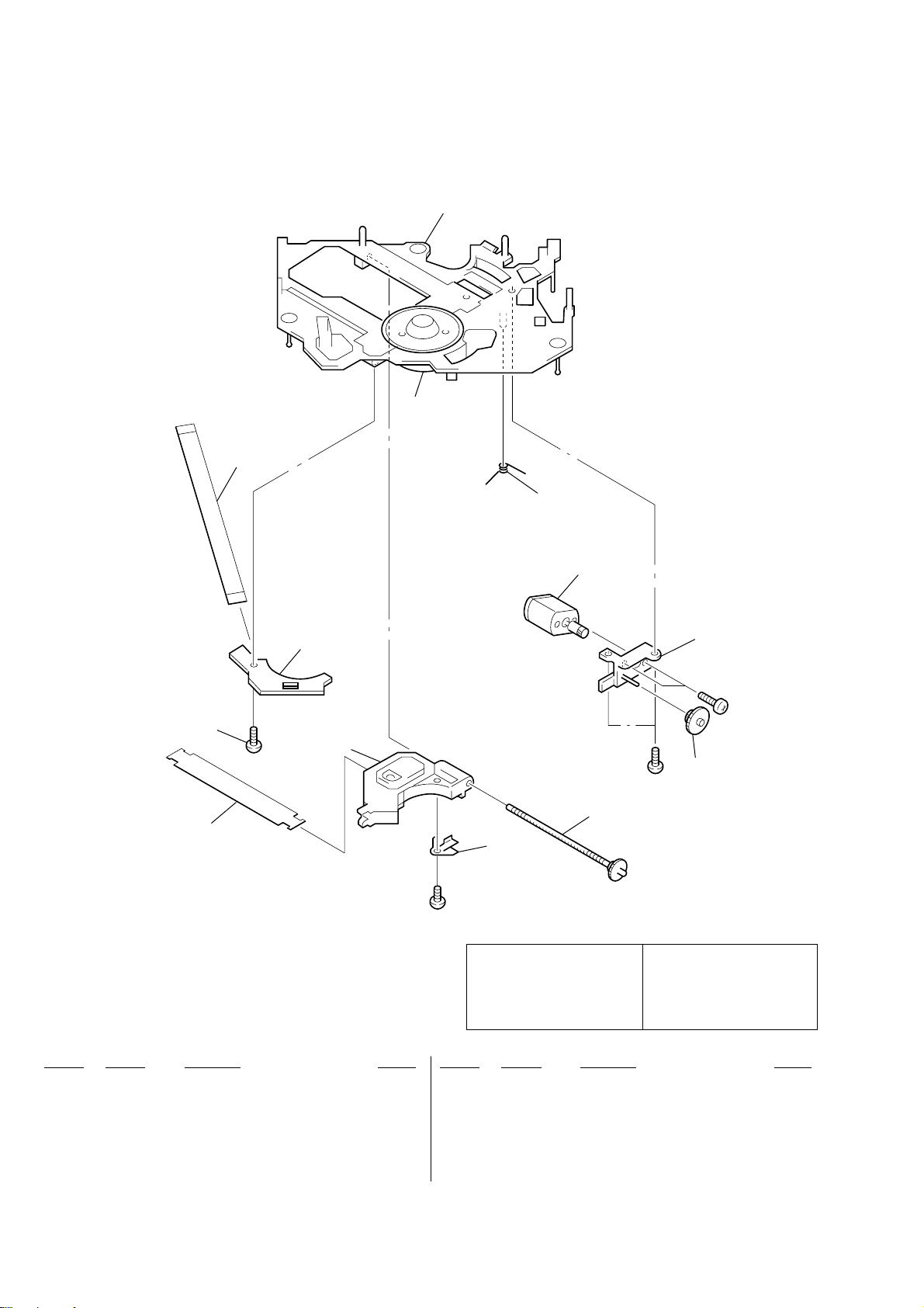
Page 13
SECTION 2
DISASSEMBLY
Note : This set can be disassemble according to the following sequence.
SET
2-5. CHASSIS (T) SUB ASSY
2-1. FRONT PANEL ASSY
(Page 13)
(Page 15)
CDX-L300/L460X
2-2. CD MECHANISM BLOCK
(Page 14)
2-3. MAIN BOARD
(Page 14)
2-4. HEAT SINK
(Page 15)
2-6. LEVER SECTION
(Page 16)
2-8. SHAFT ROLLER ASSY
(Page 17)
2-9. FLOATING BLOCK ASSY
(Page 17)
2-10. OPTICAL PICK-UP BLOCK
(Page 18)
Note : Follow the disassembly procedure in the numerical order given.
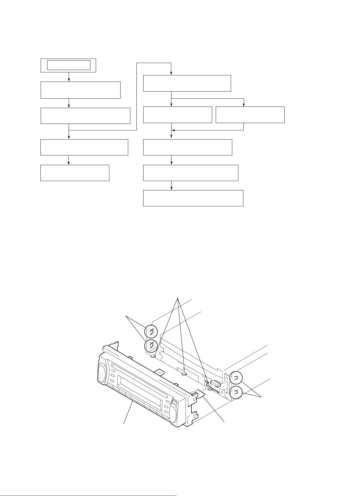
2-1. FRONT PANEL ASSY
2-7. SERVO BOARD
(Page 16)
2
claws
4
front panel assy
claws
3
CNP801
1
claws
13
Page 14
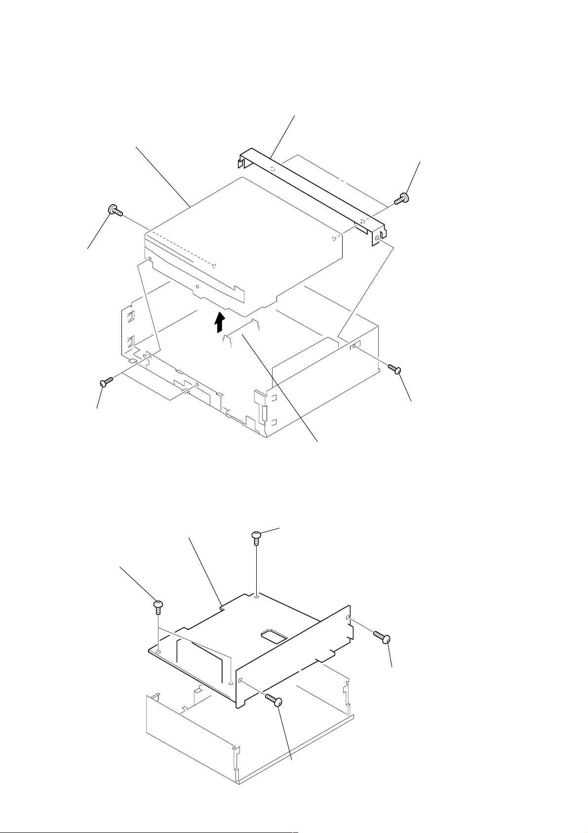
CDX-L300/L460X
8
6
2-2. CD MECHANISM BLOCK
6
CD mechanism block
2
PTT 2.6x6
8
bracket (CD)
7
PTT 2.6x
3
PTT 2.6x6
2-3. MAIN BOARD
4
screws (+BTT)
4
5
MAIN board
3
screw (+BTT)
5
CNP701
1
PTT 2.6x6
14
1
PTT 2.6x8
2
PTT 2.6x
Page 15
8
2-4. HEAT SINK
CDX-L300/L460X
6
heat sink
5
PTT 2.6x
4
PTT 2.6x8
2-5. CHASSIS (T) SUB ASSY
1
Unsolder the
lead wires.
2
P 2x3
1
PTT 2.6x8
2
PTT 2.6x8
3
PTT 2.6x12
3
P 2x3
4
chassis (T) sub assy
black
red
white
15
Page 16
CDX-L300/L460X
k
2-6. LEVER SECTION
6
lever (R)
3
tension spring (LR)
7
lever (L)
5
guide (disc)
1
special screw
2
IN SELF SW board
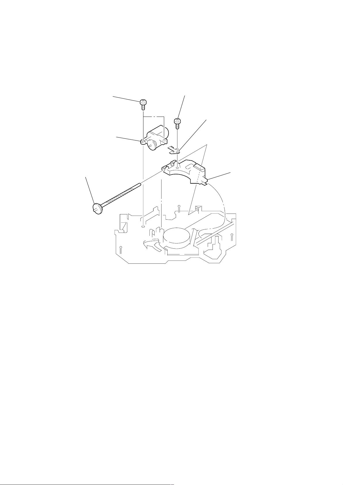
2-7. SERVO BOARD
2
4
loading motor assy
4
claws
5
special screws
Removal the solders.
1
CN3
3
P 2x3
7
SERVO board
6
special screw
8
connector
16
optical pick-up bloc
Page 17
Fig. 1
1
tension spring (RA)
2
arm (roller)
3
retaing ring (RA)
4
shaft retainer
5
shaft roller assy
retaing ring (RA)
arm
arm
washer
washer
shaft retainer
shaft retainer
2-8. SHAFT ROLLER ASSY
• When installing, take note of the positions
arm (roller) and washers. (Fig. 1)
CDX-L300/L460X
2-9. FLOATING BLOCK ASSY
7
compression spring (FL)
5
Turn loading ring in the
direction of the arrow.
1
tension spring (KF1)
6
floating block assy
8
compression spring (FL)
4
Fit lever (D) in the
direction of the arrow.
3
damper (T)
2
damper (T)
17
Page 18
CDX-L300/L460X
2-10. OPTICAL PICK-UP BLOCK
1
P 2x3
2
sled motor assy
6
shaft (feed) assy
4
P 2x3
5
spring (feed), plate
3
optical pick-up block
18
Page 19

SECTION 3
DIAGRAMS
3-1. IC PIN DESCRIPTION
• IC801 µPD780024AGK-B40-9ET (SYSTEM CONTROLLER)
Pin No. Pin Name I/O Pin Description
1 D SW I Down switch detection input
2 IN SW I Disc in switch detection input
3 PH3 I PH3 detection input (Not used in this set)
4 LM LD O Loading motor drive output (Loading)
5 LM EJ O Loading motor drive output (Eject)
6 A ATT O Power amplifier mute control output
7 ATT O Line out mute control output
8 BEEP O BEEP output
9 VSSO — Ground
10 VDDO — Power supply pin (+5 V)
11 VOL CLK O Electric volume clock output
12 VOL DO O Electric volume data out output
13 VOL CE O Electric volume chip enable output
14 AM ON O Tuner AM power supply control output
15 FM ON O Tuner FM power supply control output
16 NOSE I Front panel attachment detection input
17 PLL DI I PLL IC data input
18 LCD DO O LCD data output
19 LCD CE O LCD chip enable output
20 LCD CLK O LCD clock output
21 PLL CLK O PLL IC clock output
22 PLL DO O PLL IC data output
23 PLL CE O PLL IC chip enable output
24 VDD1 — Power supply pin (+5 V)
25 AVSS — Ground
26 ST IND I FM STEREO detection input
27 FUN SEL I Function select input
28 S METER I S meter signal input
29, 30 KEY0, 1 I A/D key input 0, 1
31 TEL ATT I Attenuator signal input
32 DST SEL I Destination select input
33 TEST I Force test mode input
34 AVREF — A/D converter power supply pin (+5 V)
35 AVDD — A/D converter power supply pin (+5 V)
36 RESET I Reset input
37 XT2 O Sub clock output (32.768 kHz)
38 XT1 I Sub clock input (32.768 kHz)
39 IC — Connect to Ground in this set.
40 X2 O Master clock output (8.38 MHz)
41 X1 I Master clock input (8.38 MHz)
42 VSS1 — Ground
43 KEY ACK I Key acknowledge detection input
44 SIRCS I SIRCS input
45 SELF SW I Self switch detection input
46 BU IN I Backup power supply detection input
47 AD ON O Key power supply control output
48 ILL ON O Illumination power supply control output
49 AMP ON O Amplifier remote power supply control output
50 CDM ON O CD mechanism deck power supply control output
51 XCD ON O CD DSP IC 16 MHz X’tal ON/OFF control output
52 TU ON O Tuner power supply control output
CDX-L300/L460X
19
Page 20

CDX-L300/L460X
Pin No. Pin Name I/O Pin Description
53 P.ON O System power supply control output
54 X SO O CD DSP IC serial data output
55 X SI I CD DSP IC serial data input
56 X SCK O CD DSP IC serial clock output
57 RFOK I CD servo IC RFOK signal input
58 X RST O CD DSP IC reset control output
59 ACC IN I Accessory power supply detection input
60 AO O CD servo IC command/pallameter discrimination signal output
61 STB O CD servo IC data strobe signal output
62 XEN O CD DSP IC X’tal control output
63 L SW I Limit switch detection input
64 PH1 I PH1 detection input (Not used in this set)
20
Page 21

3-2. BLOCK DIAGRAM — CD SECTION —
OPTICAL PICK-UP
KSS-720A
RF AMP,DIGITAL SERVO
DIGITAL SIGNAL PROCESSOR
IC1(MG-393X-121//K)
IC1(MG-393XA-121//K)
CDX-L300/L460X
PD
LD
A
C
B
D
E
F
FOCUS
COIL
I-V
CONV.
LD
DRIVE
Q1
B
84
D
85
A
82
C
83
E
87
F
86
PD
97
A5V
LD
98
FOCUS/TRACKING COIL DRIVE,
SLED/SPINDLE/LOADING MOTOR DRIVE
FCS-
15
FCS+
16
TRACKING
ERROR
APC
IC2(MG-393X-121//K)
IC2(MG-393XA-121//K)
FOCUS
COIL
DRIVE
(Page 22)
MAIN
LOUT
RF
EQ
FORCUS
ERROR
FD
26
EFM
DEMOD
SERVO
CTL
FDTDSD
62 63 64 65
MD
D/A
CONV
DSUB CODE
PROCESS
I/F
OSC
23 24
X1
16.9344MHz
ROUT
PACK
TSTB
TSCK
TSI
SCK
STB
RST
RFOK
XTALEN
16
12
R-CH
52
56
55
54
SI
8
SO
7
6
5
AO
4
3
2
9
SW1
(DOWN)
CDL
SECTION
A
SYSTEM CONTROL
54
X_SO
55
X_SI
56
X_SCK
61
STB
60
A0
58
X_RST
57
RFOK
XEN
62
1
D_SW
IC801(1/3)
TRACKING
COIL
M902
(SLED)
M901
(SPINDLE)
M903
(LOADING)
45
2
63
4
5
50
51
SELF_SW
IN_SW
L_SW
LM _LO
LM_ EJ
CDM ON
XCD_ON
RESET
IC902
36
1
S581
(RESET)
RESET
2
U_COM+5V
• Signal path
:CD
• R-ch is omitted due to
same as L-ch.
(DISC IN)
POWER
CONTROL
Q905,906
BATT
SW2
(SELF)
SW3
SW4
(LIMIT)
POWER
CONTROL
Q921
TRK+
17
TRK-
18
SL-
M
13
SL+
14
SP+
M
11
SP-
12
LD-
M
9
LD+
10
TRACKING
COIL
DRIVE
SLED
MOTOR
DRIVE
SPINDLE
MOTOR
DRIVE
LOADING
MOTOR
DRIVE
TD
23
SD
5
MD
6
LOAD
1
EJECT
2
A_5V
AU_5V
D_5V
DR_6V
REG
Q910,D910
REG
Q907,D908
D909
21 21
Page 22

CDX-L300/L460X
3-3. BLOCK DIAGRAM — TUNER SECTION —
CNJ601
(ANTENNA)
TU+B
FM POWER
CONTROL
Q605,606
AM POWER
CONTROL
Q603,604
TUNER UNIT
TU601
2 16
FM_ANT L-CH
1
AM_ANT
13
FM/AM_VCC
•
25
FM_VCC
12
9
AM_VCC
R-CH
DET_OUT
AM_DX/LCL
FM/AM_OSC
FM_VT
AM_VT
OSC-IN
IF_COUNT
S_METER
SD/ST_IND
PJ401
L
AUDIO OUT REAR
CNP501
10
12
11
15
17
19
18
16
1
FL+
9
FL–
2
RL+
RL–
4
FR+
FR–
3
RR+
RR–
7
ACC
TEST
5
AMP REM
6
ANT REM
8
GND
+B (BATT)
R
(Page 21)
A
CD
D_OUT
D_IN
CK
CE
XO
XI
SW801
CDL
6
4
5
3
1
X601
10.25MHz
SECTION
17
24
3
11
6
14
19
20
21
22
R-CH
8
LCL
15
FM_VCO
16
AM_VCO
18
FM_CP
19
VT
20
AM_CP
2
OSC
10
SEEK
13
IFC
11 24
MONO
FREQUENCY
()
PLL
IC601
SELECT
FM 200k
AM 10k
FM 50k
AM 9k
ELECTRONIC VOLUME
IC401
L5
14
L1
18
L2
17
R2
21
CE
2
DI
1
CL
36
SYSTEM CONTROL
IC801 (2/3)
VOL_CLK
11
VOL_DO
12
VOL_CE
13
PLL_DI
17
PLL_DO
22
PLL_CLK
21
PLL_CE
23
S_METER
28
SD_IND
26
DST_SEL
32
LF OUT
LR OUT
RF OUT
RR OUT
ATT
BEEP
P.ON
A_ATT
ACC IN
TEST
AMP_ON
TU_ON
BU_IN
FM_ON
AM_ON
5
4
Q102
33
R-CH
34
7
8
53
6
59
33
49
52
46
15
14
MUTE
Q401,402
MUTE
CONT
COM+8V
U_COM+5V
Q101
MUTE
R-CH
D402
DELAY BATT
TU+B
Q909
BATT
ACC
CHECK
Q902
AMP POWER
CONTROL
Q911,917
BACK-UP CHECK
Q903,904,D906,907
TUNER+8V REG
Q912,913,D913
COM+8V REG
Q918,919,929,D923
U_COM+5 V REG
Q920,D930,D999
POWER AMP
12
11
AUX-IN
16
STBY
4
MUTE
22
IC101
BATT
R-CH
5
3
9
7
R-CH
F901
10A
L300 L460X
• Signal path
:FM
:AM
:CD
• R-ch is omitted due to
same as L-ch.
2222
Page 23

3-4. BLOCK DIAGRAM — DISPLAY SECTION —
CDX-L300/L460X
KEY MATRIX
S501-511,
S512-521
D914
KEY 0
KEY 1
KEY
ACTIVE
Q916
X802
32.768kHz
SYSTEM CONTROL
IC801 (3/3)
KEY 0
29
KEY 1
KEY ACK
43
AD ON
47
XT2
37
XT1
38
LCD DO
LCD CLK
LCD CE
ILL ON
LCD DRIVE
IC551
1
SEG1
SEG52
COM1
COM2
INH
SWITCH
Q915
|
23
|
•
25
|
53
64
•
•
63
ILL+B
ILL + B
LCD
LCD501
D561-581
LED501-504
KEY
()
ILLUMINATION
LCD BACK
()
LIGHT
DATA
18
20
1930
48
X2
40
X1
41
DATA
62
CLK
61
CE
60
ILL POWER
CONTROLLER
Q914
BATT
X801
8.38MHz
CLK
CE
INITIAL
RESET
D552
57
23
Page 24

CDX-L300/L460X
3-5. CIRCUIT BOARDS LOCATION
SERVO board
• Waveforms
— Servo Board —
(MG-393X-121//K)
(MODE: CD PLAY)
IN SELF SW board
DISPLAY board
SL SW board
• Waveforms
— Servo Board —
(MG-393XA-121//K)
(MODE: CD PLAY)
SPEAKER board
tuner unit
(TU601)
MAIN board
— Main Board —
1
2
3
4
5
16.9344MHz
IC1
wd
22.7µsec
IC1
ts
IC1
uj
Approx. 1Vp-p
IC1
oa
(XTAL)
(PACK)
(RFO)
(FEO)
4.4Vp-p
3Vp-p
1.2Vp-p
0V
1
2
3
4
5
16.9344MHz
IC1
wd
22.7µsec
IC1
ts
IC1
uj
Approx. 1Vp-p
IC1
oa
(XTAL)
(PACK)
(RFO)
(FEO)
4.4Vp-p
3Vp-p
1.2Vp-p
0V
1
2
32.768kHz
IC801
8.38MHz
IC801
ej
r;
3.8Vp-p
(XT2)
5Vp-p
(X2)
24
Approx. 400mVp-p
od
(TEO)
IC1
0V
Approx. 400mVp-p
od
(TEO)
IC1
0V
Page 25

3-6. SCHEMATIC DIAGRAM • Refer to page 24 for Waveforms.
— CD MECHANISM SECTION (MG-393X-121//K) — • Refer to page 36 for IC Block Diagrams.
CDX-L300/L460X
IC B/D
IC B/D
(Page 33)
Note:
• Voltage and waveforms are dc with respect to ground
under no-signal (detuned) conditions.
no mark : CD PLAY
25 25
Page 26

CDX-L300/L460X
THIS NOTE IS COMMON FOR PRINTED WIRING
BOARDS AND SCHEMATIC DIAGRAMS.
(In addition to this, the necessary note is
printed in each block.)
for schematic diagram:
• All capacitors are in µF unless otherwise noted. pF: µµF
50 WV or less are not indicated except for electrolytics
and tantalums.
• All resistors are in Ω and 1/
specified.
• % : indicates tolerance.
f
•
• C : panel designation.
Note:
The components identified by mark 0 or dotted
line with mark 0 are critical for safety.
Replace only with part
number specified.
• A : B+ Line.
• Power voltage is dc 14.4V and fed with regulated dc power
• Voltages are taken with a VOM (Input impedance 10 MΩ).
• Waveforms are taken with a oscilloscope.
• Circled numbers refer to waveforms.
• Signal path.
: internal component.
supply from ACC and BATT cords.
Voltage variations may be noted due to normal produc-
tion tolerances.
Voltage variations may be noted due to normal production tolerances.
F : FM
f : AM
J : CD
4
W or less unless otherwise
Note:
Les composants identifiés par
une marque 0 sont critiques
pour la sécurité.
Ne les remplacer que par une
piéce portant le numéro
spécifié.
3-7. PRINTED WIRING BOARDS • Refer to page 24 for Circuit Boards Location.
— CD MECHANISM SECTION (MG-393X-121//K) —
for printed wiring boards:
• X : parts extracted from the component side.
• Y : parts extracted from the conductor side.
• x : parts mounted on the conductor side.
a
•
• : Pattern from the side which enables seeing.
Caution:
Pattern face side: Parts on the pattern face side seen from the
(Side B) pattern face are indicated.
Parts face side: Parts on the parts face side seen from the
(Side A) parts face are indicated.
: Through hole.
(The other layer’s patterns are not indicated.)
2626
Page 27

(Page 31)
CDX-L300/L460X
• Semiconductor
Location
Ref. No. Location
IC1 D-2
IC2 G-2
Q1 B-3
27 27
Page 28

CDX-L300/L460X
3-8. PRINTED WIRING BOARDS • Refer to page 24 for Circuit Boards Location.
— CD MECHANISM SECTION (MG-393XA-121//K) —
CN2
23456789101112
1
A
B
C
D
SW1
E
F
G
H
I
J
2828
Page 29

CDX-L300/L460X
A
B
C
D
E
F
G
H
1
I
234567891011121314
• Semiconductor
Location
Ref. No. Location
IC1 E-7
IC2 H-7
Q1 C-6
SW4
TP66
TP73
TP53
TP64
TP86
TP87
TP75
TP47
TP69
TP57
R20
R22
FB6
R21
TP68
TP54
TP76
FB7
FB3
TP48
TP85
TP50
TP51
TP52
TP56
TP58
TP61
TP74
TP62
CN1
TP49
TP7
C44
TP91
TP90
TP19
CN3
TP63
TP60
TP59
TP71
R17
TP72
TP80
TP8
R19
C26
TP77
R26
C4
TP9
TP70
C40
TP55
C27
C37
TP78
FB1
TP20
R30
Q1
C6
R3
C25
C34
C1
R29
C3
R18
C41
C45
X1
TP92
TP17
C29
R7
R6
TP16
TP79
C17
C22
C21
C16
C36
TP34
C5
C43
TP11
C9
C10
C8
TP36
R24
R25
TP12
TP35
FB4
FB2
TP39
IC2
C15
IC1
TP46
C38
TP82
TP81
C11
TP37
TP38
TP40
TP30
C14
TP45
TP83
TP43
TP42
TP32
R15
R12
R10
TP26
C30
TP28
TP27
TP84
C13
C18
TP23
C35
TP41
TP29
R5
R9
TP44
TP21
TP10
TP89
TP88
TP18
TP3
TP2
TP1
C20
C19
R8
R14
C23
C24
TP22
TP24
TP25
TP6
SW3
(Page 31)
SW2
TP5
TP4
J
29 29
Page 30

CDX-L300/L460X
3-9. SCHEMATIC DIAGRAM • Refer to page 24 for Waveforms.
— CD MECHANISM SECTION (MG-393XA-121//K) —• Refer to page 36 for IC Block Diagrams.
CN2
Q1
TP9 TP8
R3 R26
C3 C6
C4
TP7
TP92
M902
M901
SW4
SW3
SW2
CN13
M903
TP87
TP86
CN3
SW1
TP4
TP2
TP3
TP77
TP78
C1 C5
TP81
TP82
TP83
TP84
TP85
TP1
TP5
R29
R30
TP79
TP80
C43
C20 C23
C19
R9
C24
TP10
C13
R5
C10
TP12 C9
TP11
C18
TP89
C14
C11
C15
C8
C16
TP24
TP25
TP22
TP23
R8
IC B/D
C17
C40
FB1
C41
TP6
R7
TP21
TP18
R6
TP17
TP20
TP16
TP19
R24
R25
C22
C21
IC2
TP88
IC1
C25
C29
C34
C45
C27
C26
TP32
TP30
R15
R12
R10
R14
TP90
C30
TP91
TP27
TP29
TP26
TP28
C37
FB4
FB2
C35
TP45
TP44
TP43
TP42
TP41
TP40
TP39
TP38
TP37
TP46
C38
TP36
TP35
TP34
C36
C44
CN1
TP61
TP76
TP60
TP75
TP59
TP74
TP58
TP73
TP57
TP72
TP56
TP71
TP55
TP70
TP54
TP69
TP53
TP68
TP52
TP51
TP50
TP64
TP49
TP48
TP63
TP47
TP62
(Page 33)
R22
R21
R18
R19
R20
R17
TP66
FB7
FB6
X1
FB3
IC B/D
Note:
• Voltage and waveforms are dc with respect to ground
under no-signal (detuned) conditions.
no mark : CD PLAY
3030
Page 31

( M G - 3 9 3 X A )
( M G - 3 9 3 X )
3-10. PRINTED WIRING BOARD — MAIN SECTION — • Refer to page 24 for Circuit Boards Location.
CDX-L300/L460X
A
B
C
D
E
F
G
H
J
1
L669
TU601
C603
C604
R602
C605
C606
C620
JW13
C848
C608
I
JW2
JW1
23456789101112131415
PJ401
CNJ601
C901
D901
D906
R911
JW65
JW62
JW94
Q912
R918
SW801
Q921
R931
R920
C916
JW51
D907
Q920
JR903
JW80
D908
C905
Q913
R930
JW52
R917
Q915
R924
C915
Q917
D909
D999
R925
Q907
JW56
TH901
R926
JW55
L901
JW61
R912
C914
R927
R933
R932
D913
R928
JW82
JW53
JW54
R929
JW83
88
JW
(Page 27)
(Page 29)
92
JW
91
87
JW
86
JW
85
JW
JW
90
JW
89
JW
• Semiconductor Location
Ref. No. Location
D401 D-5
D402 D-6
Ref. No. Location
IC801 H-7
IC902 I-9
D444 D-6
D445 D-6
D446 D-6
D604 E-2
D666 F-4
D810 I-4
D901 C-9
D903 C-9
D904 C-9
D906 D-9
D907 D-9
D908 D-10
D909 F-10
D910 E-7
D913 G-11
D914 I-8
D915 C-8
D916 C-6
D917 C-8
D918 C-6
D919 C-8
D920 B-7
D921 B-7
D922 C-8
D923 F-8
D930 H-9
D999 G-10
Q101 C-3
Q102 C-3
Q201 C-4
Q202 C-4
Q401 D-6
Q402 D-6
Q603 H-3
Q604 H-4
Q605 H-2
Q606 H-4
Q902 E-9
Q903 E-9
Q904 E-9
Q905 G-8
Q906 G-9
Q907 C-10
Q909 E-9
Q910 E-8
Q911 G-9
Q912 G-9
Q913 G-10
Q914 H-9
Q915 H-10
Q916 H-8
Q917 E-10
Q918 F-8
C635
R620
R622
L605
C666
R623
JW14
D601
JW33
JW32
R609
D604
R603
C650
R621
C651
JW15
R628
Q605
JW35
CP601
L601
JR610
R614
C627
R601
C619
JW36
JW17
R604
R109
C609
C610
C612
C613
C615
C617
R608
JW16
Q603
R113
R115
JW84
JW6
R107
Q101
C108
C114
C115
R613
C611
C614
R607
C618
C622
C621
R616
R617
CNP802
C103
JR602
C625
JW18
R618
R108
JW34
L603
R606
IC601
X601
C623
C105
R105
Q102
R110
L604
C842
JW37
Q202
C104
C110
C111
C113
C116
R612
R611
C205
R106
R210
D666
JR1
C631
C633
R619
C624
JW3
JW4
R208
R209
C204
C626
Q606
R207
IC401
C117
JW31
C841
C809
R206
R205
JW28
R610
JW19
R605
JW99
Q201
C203
JW20
C119
Q604
D810
JW30
C118
JW97
C652
R615
JW107
C407
C101
C201
C219
JW21
R809
JW38
C435
C213
JW29
C845
C202
JR101
C102
JW22
JW9
JW10
D401
C218
JW23
JW11
JW106
JW12
JW108
C401
C843
C208
C214
C216
C217
JW105
JW5
JW41
JW96
R806
R824
R810
JW40
JW25
JW27
JW26
R811
JW39
C210
C211
R213
R215
C215
JW24
R807
R812
R714
R841
R840
R813
R814
R922
JW43
IC101
C432
C426
D444
C706
R716
C707
CNP701
JW67
C844
R408
R808
R843
C810
D445
C847
R842
JW42
D918
R410
R444
R407
C812
JW7
JW45
Q401
R401
R822
C701
R815
D402
D446
R923
JW44
D916
Q402
IC801
R704
JW8
JW46
JW47
JW48
JW64
R705
R710
JW98
C803
JW68
C907
R706
R708
R709
R711
JW72
L703
C702
C703
C704
R707
X802
R404
C801
JW49
JW59
JW60
D910
L701
D921
D920
JW57
JW58
JW95
C804
C802
X801
JW69
D919
D922
D917
D915
L702
R934
JW71
R802
D923
C849
C806
C919
JW73
D914
CNP501
Q910
Q919
C846
JW74
R921
JW75
JW50
C902
JR901
JW63
Q918
JW66
Q916
JW76
R901
C904
R908
Q909
Q911
JW77
JW110
Q902
Q929
Q905
R818
JW78
R906
D903
R907
JW93
Q914
D904
R909
R910
Q904
Q903
R913
JW126
JR929
Q906
C909
D930
R919
JW81
R817
R819
JW79
IC902
Q919 F-8
IC101 B-6
IC401 D-4
IC601 F-3
Q920 G-9
Q921 F-9
Q929 F-8
(Page 34)
31 31
Page 32

CDX-L300/L460X
Ver 1.3
3-11. SCHEMATIC DIAGRAM — MAIN SECTION (1/2) — • Refer to page 36 for IC Block Diagrams.-
CNJ601
L605
TU601
CP601
L669
L601
C635
JW13
C604
C666
D601
C605
R601
JR610
C603
R620
R622
C650 C651R621
C606
R602
R623
PJ401
R603
C619
R609
L603
C614
C615
C617
C618
C609
C610
C612
C613
R607
C620
R608
C621
C103
C104
C203
C204
JR602
R606
C611
R209
R210
C622
C623
R109
R110
R107
R108
R207
R208
Q101
Q102
Q201
Q202
IC601
IC B/D
X601
C624
R613
C626
D666
L604
R619
C625
R610
R611
C631
C105
C205
Q401
Q402
R612
C633
R105
R206
D402
C432
R106
R205
R213
R215
C215
C435
R410
D401
C217
D446
C210
C211
C213
C214
C218
C216
C219
C208
D444
R444
D445
IC B/D
C401
R401
R404
IC401
C201
C202
C102
C101
C114
C407
C108
C111
C113
C116
C119
C117
JR101
C110
C426
R408
R113
R115
C115
IC101
D922 11ES2-TA1B
D921 1SR154-400TE
D920 1SR154-400TE
D919 11ES2-TA1B
D917 11ES2-TA1B
D918 11ES2-TA1B
D915 11ES2-TA1B
D916 11ES2-TA1B
R407
C706
C707
R906
D903
D904
C902
R901
C901
CNP501
L901
D901
C608
C848
R628
D604
R604
C627
R605
R614
Q603
Q604
R615
R616
C841
Q605
Q606
R617
C842
R618
C118
R716 R714
(Page 33)
Note:
•Voltage is dc with respect to ground under no-signal
(detuned) condition.
no mark : FM
(): AM
<>: CD PLAY
3232
Page 33

( M G - 3 9 3 X )
( M G - 3 9 3 X A )
3-12. SCHEMATIC DIAGRAM — MAIN SECTION (2/2) — • Refer to page 24 for Waveforms.
(Page 25)
C847
C844
R711
R710
R709
CNP701
(Page
30)
R704
R705
R706
R707
R708
C701
C704
C703
C702
L703
L701
L702
(Page 32)
Q903
Q904
R910
R911
D906
D907
Q902
R909
R908
R907
CDX-L300/L460X
C904
JR901
(Page 35)
CNP802
JR1
C809
SW801
R817
R818
R802
R819
R815
R814
R813
R822
R840
R841
R842
R843
R812
R811
R810
C810
R824
C812
R922
R923
R809
D914
C801
R807R808
R806
C803
C843
Q916
X802C802
R921
C804
X801
IC801
C806
C845
C849
C916
D810
R929
R928
R927
R926
R925
R924
C846
JR903
Q914
IC902
Q915
R919
C915
R920
R918
C919
C914
C909
Q919
Q913
R934
D923
Q920
D913
R931
R917
Q918
D930
R930
Q929
Q912
D999
Q909
Q921
D910
Q910
R932
R913
C907
Q917
Q911
JR929
R933
D908
TH901
D909
Q907
Q906
R912
Q905
C905
33 33
Note:
• Voltage and waveforms are dc with respect to ground
under no-signal (detuned) conditions.
no mark : FM
( ) : AM
< > : CD PLAY
Page 34

CDX-L300/L460X
3-13. PRINTED WIRING BOARD — DISPLAY SECTION — • Refer to page 24 for Circuit Boards Location.
A
B
C
D
1
D561
D562
D563
2 3 4 5 6 7 8 9 10 11 12 13 14
R569
R570
R564
R577
R563
R580
D564
R578
R579
D565
R565
R567
R566
D566
R568
R559
R560
LED501
LED502
D567
D574
D573D569 D568D570
D572
D571
LED504
LED503
D578
R561
R562
D577
D579
D575
R571
D576
R572
R581
R583
R575
D580
R576
D581
R582
R573
R574
E
F
G
H
CNP551
S515
S501
S514
R513
R512
R511
S513
S511
S509
S512
R501
(Page 31)
JR504
S510
C551
D552
R551
R588
JR505
R552
D553
R586
D551
R510
R587
S516
C552
D554
R553
R514
C555
R515
C553
JR501
S517
LCD501
R516
S518
IC551
S519
S520
R517
R519
S521
R518
• Semiconductor Location
Ref. No. Location
D551 F-5
D552 F-4
D553 G-4
D554 G-5
D561 B-1
D562 C-1
D563 D-1
D564 B-3
R509
S503
S504
S508
Ref. No. Location
D565 C-3
D566 C-3
D567 A-6
D568 A-5
D569 A-3
D570 A-2
D571 A-10
D572 A-9
S502
R503
R502
S507
Ref. No. Location
D573 A-8
D574 A-7
D575 B-12
D576 C-12
D577 C-12
D578 A-11
D579 A-12
D580 B-13
R504
R508
R505
R506
R507
S581
S505
S506
JR503
Ref. No. Location
D581 C-13
IC551 G-7
LED501 B-4
LED502 C-4
LED503 C-11
LED504 B-11
3434
Page 35

3-14. SCHEMATIC DIAGRAM — DISPLAY SECTION —
CDX-L300/L460X
(Page 33)
CNP553
S581
JR505
R586
R587
R588
JR501
D554
CNP551
D561 D564 D568 D573 D575
LED501 LED503
D565
D562
D563
R559 R560 R561 R562
LED502
D553
R511 R512 R513 R514 R515 R516 R517 R518 R519
LED504
R565 R566 R578
D566
R577R563 R564
D569 D574
D570 D567
R567 R568
R579
R570 R575
R569
D576
R571 R581R572
D577
R580
D579
D580
R573 R574 R582
D581
D572
D571
D578
R576 R583
R552 R553
D552
C555 C553
D551
C552
C551 R551
S512 S513
R501 R502 R503 R504 R505 R506 R507 R508 R509 R510
S501
S511 S502 S503 S504 S505 S506 S507 S508 S509 S510
S514 S515
S516 S517 S518 S519 S520 S521
JR503
Note:
• Voltage is dc with respect to ground under no-signal
(detuned) condition.
no mark : FM
35 35
Page 36

CDX-L300/L460X
• IC Block Diagrams
IC1 µPD63711GC-8EU (MG-393X-121//K)
IC1 µPD63711GC-8EU (MG-393XA-121//K)
AGCO74RFI73C3T72ASY71EFM70AVDD697E DAC3687D DAC2677C DAC1667F DAC065MD64SD63TD62FD
75
AGCI
RFO
EQ2
EQ1
RF-
AGND
AVDD
REFOUT
FEO
TE-
TEO
TE2
TEC
AGND
AVDD
76
77
78
79
80
81
A
82
C
83
B
84
D
85
F
86
E
87
88
89
FE-
90
91
92
93
94
95
96
PD
97
LD
98
99
PN
100
EFM
COMPARATOR
EFM
FEOFS
TEOFS
RF
AMP BLOCK
EFM
SWITCH
DEFECT
FOK
A3T
MIRR
FEO
TEO
COMPARATOR
MICROCOMPUTER INTERFACE
AUTO GAIN
CONTROLLER
SVDRAM
PROCESSOR
DEFECT
COMPARATOR
RFENV
MIRENV
TRACKING
A/D CONVERTER
REGISTER
FOCUS
REGISTER
ADDER
MULTIPLIER
SVROM
CLV
D/A
FD/TD/SD/MD
CONTROLLER
SVCRAM
ROM
DECODER
ATEST59TEST158TEST057DGND56TSTB55TSCK54TSI53TSO52PACK51DVDD
AGND
60
61
MICROCOMPUTER INTERFACE
CD-TEXT DECODER
D/A
INTERFACE
CIRCUIT
OCTUPLED
NOISE SHAVER
OUTPUT BUFFER
SUB-CODE PROCESSOR
OSC
MEMORY
PROCESSOR
SCF
16K
SRAM
EFM DEMODULATOR
TIMING GENERATOR
DE-EMPHASIS CIRCUIT
OVERSAMPLING DIGITAL FILTER
NOISE SHAVER
OUTPUT BUFFER
DIGITAL PLL
DIGITAL
AUDIO
INTERFACE
OUTPUT PROCESSOR
ERROR
PROCESSOR
CORRECTION
C2D3
50
C2D2
49
C2D1
48
C1D2
47
C1D1
46
DGND
45
PLCK
44
MIRR/WFCK
43
RFCK
42
LOCK
41
DVDD
40
TSOI
39
C16M
38
DGND
37
TX
36
HOLD/WDCK
35
LRCK
34
LRCKIN
33
SCKO
32
SCKIN
31
DOUT
30
DIN
29
FLAG
28
EMPH
27
DVDD
26
FWD
REV
LDCONT
IN1
IN2
PREVCC
POWVCC
VOL–
VOL+
VO2–
VO2+
VO1–
VO1+
IC2 BA5810FP-E2 (MG-393X-121//K)
IC2 BA5810FP-E2 (MG-393XA-121//K)
1
PS
2
3
4
5
6
(PRE.LOADING)
7
8
9
10
10k
11
12
10k
10k
13
14
10k
X3
PREVCC
POWVCC12
(CH1.CH2)
–
+
+
–
–
+
+
–
POWER
SAVE
10k
10k
10k
10k
LOADING PRE
7.5k
16k
LEVEL
SHIFT
FWD REV
7.5k
16k
–
+
LEVEL
SHIFT
7.5k
–
+
+
LEVEL
SHIFT
–
+
LEVEL
SHIFT
IC601 TB2118F (EL-S)
16k
–
7.5k
16k
POWVCC34
10k
10k
10k
10k
+
–
+
–
CH1-4
MUTE
(CH3,CH4)
–
+
+
–
–
+
+
–
10k
10k
10k
10k
28
27
26
25
24
23
22
21
20
19
18
17
16
15
BIAS
OPIN4+
OPIN4–
OPOUT4
OPIN3+
OPIN3–
OPOUT3
MUTE
POWVCC
GND
VO3–
VO3+
VO4–
VO4+
1
DGND
2
RFOK
3
4A05
6
RST
STB
7SO8SI9
SCK
XTALEN
10
DVDD
11
DAVDD
12
ROUT
13
DAGND
REGC
1514
16
DAGND
17
18R+19R–20L+21L–22
LOUT
DAVDD
23
XVDD
XTAL24XTAL
25
XGND
OSC
D_IN
D_OUT
LCL
I/O-2
SEEK
MONO
VDD2
XO
1
2
CE
3
4
5
CK
6
SR
7
8
9
10
11
VDD2
12
SERIAL
INTERFACE
I/O
PORT
OUTPUT
PORT
BUFFER
ON/OFF
40BIT SHIFT
REGISTER
18BIT
18BIT
22BIT
OSCILLATOR
REFERENCE
DIVIDER
REF
PHASE
COMPARATOR
SIG
12BIT
PROGRAMMABLE
COUNTER
20BIT
IF COUNTER
SEEK/RECP
SEEK/RECP
PRESCALLER
+
REGULATOR
4BIT SWALLOW
COUNTER
AMP
AMP
VCC
–
+
+
+
–
AMP
VDD
24
23
22
21
20
19
18
17
16
15
14
13
XI
A-GND
REG
VCC
AM_CP
VT
FM_CP
D-GND
AM_VCO
FM_VCO
VDD
IFC
3636
Page 37

IC401 LC75421M-TLM-E
DI
1
CE
2
VSS
3
LROUT
4
LFOUT
5
CDX-L300/L460X
CL
36
VDD
35
RROUT
34
RFOUT
33
LFIN
LOUT
LSB
LBASS2
LBASS1
LTRE
LIN
LSELO
+
–
6
7
8
9
10
11
12
13
L5
14
L4
15
+
–
CCB
INTERFACE
+
–
+
–
–
CONTROL
CIRCUIT
+
LOGIC
CIRCUIT
CONTROL
CIRCUIT
+
–
+
–
+
–
+
–
LVREF RVREF
+
–
+
–
+
–
RFIN
32
ROUT
31
RSB
30
29
RBASS2
RBASS1
28
RTRE
27
RIN
26
25
RSELO
24
R5
23
R4
16
L3
L2
17
–
L1
18
+
–
+
22
R3
21
R2
20
R1
19
VREF
37
Page 38

CDX-L300/L460X
NOTE:
• The mechanical parts with no reference
number in the exploded views are not supplied.
• Items marked “*” are not stocked since
they are seldom required for routine service.
Some delay should be anticipated
when ordering these items.
• -XX and -X mean standardized parts, so
they may have some difference from the
original one.
4-1. CHASSIS SECTION
3
SECTION 4
EXPLODED VIEWS
• Color Indication of Appearance Parts
Example :
KNOB, BALANCE (WHITE) ... (RED)
• Accessories and hardware (# mark) list are
given in the last of this parts list.
MG-393X-121//K
MG-393XA-121//K
4
R
Parts Color Cabinet’s Color
5
The components identified by
mark 0 or dotted line with mark
R
0 are critical for safety.
Replace only with part number
specified.
Les composants identifiés par une
marque 0 sont critiques pour
la sécurité.
Ne les remplacer que par une piéce
portant le numéro spécifié.
#1
#2
#2
#2
6
2
7
10
11
9
#3
TU601
#2
#2
#2
8
F901
12
6
#1
#1
#1
Ref. No. Part No. Description Remark
* 1 3-224-612-11 CHASSIS (CD)
2 3-224-309-21 COVER
3 1-776-206-21 CORD (WITH CONNECTOR) (POWER)
* 4 3-024-285-01 CUSHION (RUBBER)
* 5 3-041-173-11 BRACKET (CD)
6 3-922-535-11 SCREW (+BTT)
7 A-3283-234-A MAIN BOARD, COMPLETE (L460X)
7 A-3283-238-A MAIN BOARD, COMPLETE (L300)
38
1
Ref. No. Part No. Description Remark
* 8 3-224-613-01 HEAT SINK
* 9 3-019-565-01 BRACKET (IC)
10 1-683-602-11 SPEAKER BOARD
11 3-041-261-11 BRACKET (TR)
* 12 3-048-259-01 SHEET (E)
F901 1-532-877-11 FUSE (BLADE TYPE) (AUTO FUSE) 10A
TU601 A-3220-835-A TUNER UNIT (TUX-010)
Page 39

4-2. FRONT PANEL SECTION
CDX-L300/L460X
#4
63
53
62
59
60
58
LCD501
64
61
57
#4
65
56
55
52
51 X-3381-455-1 PANEL SUB ASSY, FRONT (L460X)
51 X-3381-476-1 PANEL SUB ASSY, FRONT (L300)
52 3-224-605-01 BUTTON (SEEK/AMS)
53 3-224-604-01 BUTTON (+/–) (L300)
53 3-224-604-11 BUTTON (+/–) (L460X)
54 3-224-601-01 BUTTON (EJECT)
55 3-224-603-01 BUTTON (OFF)
56 3-224-600-01 BUTTON (1-6)
57 3-224-602-01 BUTTON (SOURCE)
54
51
Ref. No. Part No. Description RemarkRef. No. Part No. Description Remark
* 58 3-224-609-02 PLATE (LCD), GROUND
59 3-224-610-11 SHEET (LCD), DIFFUSION
60 X-3381-070-1 HOLDER (LCD) ASSY
61 A-3283-240-A DISPLAY BOARD, COMPLETE
62 3-224-617-01 BUTTON (RESET)
* 63 3-227-293-01 SHEET (LCD)
* 64 3-229-751-01 SHEET (LCD.UP)
65 1-765-143-41 WIRE (FLAT TYPE) (10 CORE) (CNP553)
LCD501 1-804-300-21 DISPLAY PANEL, LIQUID CRYSTAL
39
Page 40

CDX-L300/L460X
Ver 1.2
4-3. CD MECHANISM SECTION (1)
(MG-393X-121//K)
101
115
104
114
109
116
103
#8
102
#8
107
106
105
111
114
113
108
C
M903
#7
#7
110 3-040-040-01 ARM (ROLLER)
* 111 A-3283-048-A SERVO BOARD, COMPLETE
112 3-221-779-01 BRACKET (MOTOR)
113 3-040-034-01 SPRING (RA), TENSION
114 3-040-042-01 WASHER
#8
#6
112
105
C
110
Ref. No. Part No. Description Remark Ref. No. Part No. Description Remark
* 101 1-676-709-11 IN SELF SW BOARD
102 3-040-039-01 CHASSIS (T)
103 3-040-038-01 SPRING (LR), TENSION
104 3-040-050-01 LEVER (L)
105 3-040-022-01 RETAINER (ROLLER), SHAFT
106 3-040-044-01 ROLLER (S)
107 3-040-067-01 LEVER (R)
108 A-3301-980-A SHAFT ROLLER ASSY
109 3-040-037-01 GUIDE (DISC)
40
115 3-043-880-01 RING (RA), RETAINING
116 3-044-206-11 SCREW, SPECIAL
M903 A-3315-039-A MOTOR SUB ASSY, LO (LOADING)
Page 41

4-4. CD MECHANISM SECTION (2)
(MG-393X-121//K)
CDX-L300/L460X
157
158
163
154
162
D
160
155
151
156
157
164
not supplied
153
161
D
159
152
152
152
Ref. No. Part No. Description Remark Ref. No. Part No. Description Remark
151 3-040-025-01 ARM, CHUCKING
152 3-040-031-01 DAMPER (T)
153 3-040-056-01 LEVER (D)
154 3-040-024-01 RETAINER (DISC)
155 3-040-054-01 WHEEL (LW), WORM
156 3-040-026-01 SPRING (CH), TENSION
157 3-040-032-01 SPRING (FL), COMPRESSION
158 3-040-033-01 SPRING (KF1), TENSION
159 A-3307-422-A CHASSIS (M) COMPLETE ASSY
160 3-040-059-01 SPRING (TR), TENSION
161 3-040-057-01 LEVER (LOCK)
162 3-040-058-01 GEAR (MDL)
163 3-040-052-01 WHEEL (U), WORM
164 3-040-051-01 LEVER (TR)
41
Page 42
CDX-L300/L460X
4-5. CD MECHANISM SECTION (3)
(MG-393X-121//K)
207
201
M901
209
211
208
210
#9
206
202
M902
205
#8
203
#5
204
The components identified by
mark 0 or dotted line with mark
0 are critical for safety.
Replace only with part number
specified.
Ref. No. Part No. Description Remark Ref. No. Part No. Description Remark
201 X-3378-480-1 CHASSIS (OP) ASSY (including M901)
202 3-040-029-01 SPRING (SL), TORSION
203 3-040-045-01 BASE (DRIVING)
204 3-040-194-01 GEAR (MIDWAY)
205 A-3301-983-A SHAFT (FEED) ASSY
206 3-040-030-01 SPRING (FEED), PLATE
207 1-677-182-11 MOTOR FLEXIBLE BOARD
* 208 1-676-708-11 SL SW BOARD
209 3-909-607-01 SCREW
0 210 8-820-103-11 PICK-UP, OPTICAL KSS-720A/C-RP
211 1-676-707-11 PICK-UP FLEXIBLE BOARD
M902 A-3301-985-A MOTOR ASSY, SLED (SLED)
Les composants identifiés par une
marque 0 sont critiques pour la
sécurité.
Ne les remplacer que par une piéce
portant le numéro spécifié.
42
Page 43

4-6. CD MECHANISM SECTION (1)
(MG-393XA-121//K)
CDX-L300/L460X
101
115
104
114
109
116
103
#8
102
#8
107
106
105
114
111
105
C
117
113
C
110
M903
#7
108
Ref. No. Part No. Description Remark Ref. No. Part No. Description Remark
101 1-683-283-11 IN SELF SW BOARD
102 3-040-039-02 CHASSIS (T)
103 3-040-038-01 SPRING (LR), TENSION
104 3-040-050-01 LEVER (L)
105 3-040-022-01 RETAINER (ROLLER), SHAFT
#7
110 3-040-040-02 ARM (ROLLER)
111 A-3283-233-A SERVO BOARD, COMPLETE
112 3-221-779-01 BRACKET (MOTOR)
113 3-040-034-01 SPRING (RA), TENSION
114 3-040-042-01 WASHER
#8
#6
112
106 3-040-044-01 ROLLER (S)
107 3-040-067-01 LEVER (R)
108 A-3301-980-A SHAFT ROLLER ASSY
109 3-040-037-01 GUIDE (DISC)
115 3-043-880-01 RING (RA), RETAINING
116 3-044-206-11 SCREW, SPECIAL
117 1-683-284-11 FLEXIBLE BOARD
M903 A-3315-039-A MOTOR SUB ASSY, LO (LOADING)
43
Page 44

CDX-L300/L460X
4-7. CD MECHANISM SECTION (2)
(MG-393XA-121//K)
157
158
163
154
162
D
160
155
151
156
157
164
not supplied
153
161
D
159
152
152
152
Ref. No. Part No. Description Remark Ref. No. Part No. Description Remark
151 3-040-025-01 ARM, CHUCKING
152 3-040-031-01 DAMPER (T)
153 3-040-056-01 LEVER (D)
154 3-040-024-01 RETAINER (DISC)
155 3-040-054-01 WHEEL (LW), WORM
156 3-040-026-01 SPRING (CH), TENSION
157 3-040-032-01 SPRING (FL), COMPRESSION
158 3-040-033-01 SPRING (KF1), TENSION
159 A-3307-422-A CHASSIS (M) COMPLETE ASSY
160 3-040-059-01 SPRING (TR), TENSION
161 3-040-057-01 LEVER (LOCK)
162 3-040-058-01 GEAR (MDL)
163 3-040-052-01 WHEEL (U), WORM
164 3-040-051-02 LEVER (TR)
44
Page 45

4-8. CD MECHANISM SECTION (3)
(MG-393XA-121//K)
207
CDX-L300/L460X
201
M901
209
208
210
#9
206
202
M902
205
#8
203
#5
204
The components identified by
mark 0 or dotted line with mark
0 are critical for safety.
Replace only with part number
specified.
Ref. No. Part No. Description Remark Ref. No. Part No. Description Remark
201 X-3378-480-1 CHASSIS (OP) ASSY (including M901)
202 3-040-029-01 SPRING (SL), TORSION
203 3-040-045-01 BASE (DRIVING)
204 3-040-194-01 GEAR (MIDWAY)
205 A-3301-983-A SHAFT (FEED) ASSY
206 3-040-030-01 SPRING (FEED), PLATE
207 1-823-641-11 CABLE, FLEXIBLE FLAT (6 CORE)
208 1-683-282-11 SL SW BOARD
209 3-909-607-01 SCREW
0 210 8-820-103-11 PICK-UP, OPTICAL KSS-720A/C-RP
M902 A-3301-985-A MOTOR ASSY, SLED (SLED)
Les composants identifiés par une
marque 0 sont critiques pour la
sécurité.
Ne les remplacer que par une piéce
portant le numéro spécifié.
45
Page 46

CDX-L300/L460X
SECTION 5
DISPLAY
NOTE:
• Due to standardization, replacements in
the parts list may be different from the
parts specified in the diagrams or the
components used on the set.
• -XX and -X mean standardized parts, so
they may have some difference from the
original one.
• RESISTORS
All resistors are in ohms.
METAL:Metal-film resistor.
METAL OXIDE: Metal oxide-film resistor.
F:nonflammable
• Abbreviation
CND : Canadian model
393X : MG-393X-121//K
393XA: MG-393XA-121//K
Ref. No. Part No. Description Remark Ref. No. Part No. Description Remark
A-3283-240-A DISPLAY BOARD, COMPLETE
************************
1-765-143-41 WIRE (FLAT TYPE) (10 CORE) (CNP553)
* 3-224-609-02 PLATE (LCD), GROUND
3-224-610-11 SHEET (LCD), DIFFUSION
* 3-227-293-01 SHEET (LCD)
* 3-229-751-01 SHEET (LCD.UP)
< CAPACITOR >
C551 1-164-315-11 CERAMIC CHIP 470PF 5% 50V
C552 1-164-156-11 CERAMIC CHIP 0.1uF 25V
C553 1-162-927-11 CERAMIC CHIP 100PF 5% 50V
C555 1-119-866-11 CERAMIC CHIP 0.68uF 10% 10V
ELECTRICAL PARTS LIST
• Items marked “*” are not stocked since
they are seldom required for routine service.
Some delay should be anticipated
when ordering these items.
• SEMICONDUCTORS
In each case, u : µ, for example:
uA.. : µA.. uPA.. : µPA..
uPB.. : µPB.. uPC.. : µPC.. uPD.. : µPD..
• CAPACITORS
uF : µF
• COILS
uH : µH
IC551 8-759-369-90 IC LC75822ED
JR501 1-216-864-11 METAL CHIP 0 5% 1/16W
JR503 1-216-864-11 METAL CHIP 0 5% 1/16W
JR505 1-216-864-11 METAL CHIP 0 5% 1/16W
LCD501 1-804-300-21 DISPLAY PANEL, LIQUID CRYSTAL
The components identified by
mark 0 or dotted line with mark
0 are critical for safety.
Replace only with part number
specified.
Les composants identifiés par une
marque 0 sont critiques pour
la sécurité.
Ne les remplacer que par une piéce
portant le numéro spécifié.
When indicating parts by reference
number, please include the board.
< IC >
< JUMPER RESISTOR >
< LIQUID CRYSTAL DISPLAY >
< DIODE >
< CONNECTOR >
* CNP551 1-779-130-11 PIN, CONNECTOR 1P
< DIODE >
D551 8-719-073-15 DIODE SDZ5V1
D552 8-719-988-61 DIODE 1SS355TE-17
D553 8-719-067-70 DIODE SDZ6V2
D554 8-719-068-68 DIODE SDZ6V2WA
D561 8-719-053-09 LED SML-310VTT86 (SEEK/AMS m . –)
D562 8-719-053-09 LED SML-310VTT86 (SEEK/AMS + > M)
D563 8-719-053-09 LED SML-310VTT86 (Z)
D564 8-719-053-09 LED SML-310VTT86 (OFF)
D565 8-719-053-09 LED SML-310VTT86 (D-BASS)
D566 8-719-053-09 LED SML-310VTT86 (MBP)
D567 8-719-053-09 LED SML-310VTT86 (5)
D568 8-719-053-09 LED SML-310VTT86 (6)
D569 8-719-053-09 LED SML-310VTT86 (BTM)
D570 8-719-053-09 LED SML-310VTT86 (DSPL)
D571 8-719-053-09 LED SML-310VTT86 (1)
D572 8-719-053-09 LED SML-310VTT86 (2)
D573 8-719-053-09 LED SML-310VTT86 (3/REP)
D574 8-719-053-09 LED SML-310VTT86 (4/SHUF)
D575 8-719-053-09 LED SML-310VTT86 (SEL)
D576 8-719-053-09 LED SML-310VTT86 (MODE)
D577 8-719-053-09 LED SML-310VTT86 (SRC – SOURCE)
D578 8-719-053-09 LED SML-310VTT86 (SENS)
D579 8-719-053-09 LED SML-310VTT86 (ATT)
D580 8-719-053-09 LED SML-310VTT86 (VOLUME –)
D581 8-719-053-09 LED SML-310VTT86 (VOLUME +)
LED501 8-719-072-40 LED LBA676-J2K1K2 (LCD BACK LIGHT)
LED502 8-719-072-40 LED LBA676-J2K1K2 (LCD BACK LIGHT)
LED503 8-719-072-40 LED LBA676-J2K1K2 (LCD BACK LIGHT)
LED504 8-719-072-40 LED LBA676-J2K1K2 (LCD BACK LIGHT)
< RESISTOR >
R501 1-219-286-11 RES-CHIP 680 2% 1/16W
R502 1-219-286-11 RES-CHIP 680 2% 1/16W
R503 1-219-286-11 RES-CHIP 680 2% 1/16W
R504 1-218-847-11 RES-CHIP 1K 2% 1/16W
R505 1-218-851-11 RES-CHIP 1.5K 2% 1/16W
R506 1-218-851-11 RES-CHIP 1.5K 2% 1/16W
R507 1-218-855-11 RES-CHIP 2.2K 2% 1/16W
R508 1-218-859-11 RES-CHIP 3.3K 2% 1/16W
R509 1-218-863-11 RES-CHIP 4.7K 2% 1/16W
R510 1-218-867-11 RES-CHIP 6.8K 2% 1/16W
R511 1-219-286-11 RES-CHIP 680 2% 1/16W
R512 1-219-286-11 RES-CHIP 680 2% 1/16W
R513 1-219-286-11 RES-CHIP 680 2% 1/16W
R514 1-218-847-11 RES-CHIP 1K 2% 1/16W
R515 1-218-851-11 RES-CHIP 1.5K 2% 1/16W
R516 1-218-851-11 RES-CHIP 1.5K 2% 1/16W
R517 1-218-855-11 RES-CHIP 2.2K 2% 1/16W
R518 1-218-859-11 RES-CHIP 3.3K 2% 1/16W
R519 1-218-863-11 RES-CHIP 4.7K 2% 1/16W
R551 1-218-331-11 RES-CHIP 51K 5% 1/16W
R552 1-216-819-11 METAL CHIP 680 5% 1/16W
R553 1-216-857-11 METAL CHIP 1M 5% 1/16W
R559 1-216-818-11 METAL CHIP 560 5% 1/16W
R560 1-216-818-11 METAL CHIP 560 5% 1/16W
R561 1-216-818-11 METAL CHIP 560 5% 1/16W
46
Page 47

CDX-L300/L460X
DISPLAY
Ref. No. Part No. Description Remark Ref. No. Part No. Description Remark
R562 1-216-818-11 METAL CHIP 560 5% 1/16W
R563 1-216-821-11 METAL CHIP 1K 5% 1/16W
R564 1-216-821-11 METAL CHIP 1K 5% 1/16W
R565 1-216-821-11 METAL CHIP 1K 5% 1/16W
R566 1-216-821-11 METAL CHIP 1K 5% 1/16W
R567 1-216-821-11 METAL CHIP 1K 5% 1/16W
R568 1-216-821-11 METAL CHIP 1K 5% 1/16W
R569 1-216-821-11 METAL CHIP 1K 5% 1/16W
R570 1-216-821-11 METAL CHIP 1K 5% 1/16W
R571 1-216-821-11 METAL CHIP 1K 5% 1/16W
R572 1-216-821-11 METAL CHIP 1K 5% 1/16W
R573 1-216-821-11 METAL CHIP 1K 5% 1/16W
R574 1-216-821-11 METAL CHIP 1K 5% 1/16W
R575 1-216-821-11 METAL CHIP 1K 5% 1/16W
R576 1-216-821-11 METAL CHIP 1K 5% 1/16W
R577 1-216-821-11 METAL CHIP 1K 5% 1/16W
R578 1-216-821-11 METAL CHIP 1K 5% 1/16W
R579 1-216-821-11 METAL CHIP 1K 5% 1/16W
R580 1-216-821-11 METAL CHIP 1K 5% 1/16W
R581 1-216-821-11 METAL CHIP 1K 5% 1/16W
R582 1-216-821-11 METAL CHIP 1K 5% 1/16W
R583 1-216-821-11 METAL CHIP 1K 5% 1/16W
R586 1-218-847-11 RES-CHIP 1K 2% 1/16W
R587 1-218-847-11 RES-CHIP 1K 2% 1/16W
R588 1-218-847-11 RES-CHIP 1K 2% 1/16W
* 1-676-709-11 IN SELF SW BOARD (393X)
1-683-283-11 IN SELF SW BOARD (393XA)
****************
< SWITCH >
SW2 1-529-566-31 SWITCH, PUSH (1 KEY) (SELF)
SW3 1-529-566-31 SWITCH, PUSH (1 KEY) (DISC IN)
*************************************************************
A-3283-234-A MAIN BOARD, COMPLETE
(including SPEAKER BOARD) (L460X)
A-3283-238-A MAIN BOARD, COMPLETE
(including SPEAKER BOARD) (L300)
*********************
* 3-019-565-01 BRACKET (IC)
3-041-261-11 BRACKET (TR)
* 3-224-613-01 HEAT SINK
7-685-793-09 SCREW +PTT 2.6X8 (S)
7-685-795-09 SCREW +PTT 2.6X12 (S)
< CAPACITOR >
C101 1-164-346-11 CERAMIC CHIP 1uF 16V
C102 1-164-346-11 CERAMIC CHIP 1uF 16V
C103 1-104-396-11 ELECT 10uF 20% 16V
C104 1-104-396-11 ELECT 10uF 20% 16V
C105 1-162-964-11 CERAMIC CHIP 0.001uF 10% 50V
MAININ SELF SW
< SWITCH >
S501 1-572-704-31 SWITCH, KEYBOARD (Z)
S502 1-572-704-31 SWITCH, KEYBOARD (SRC – SOURCE)
S503 1-572-704-31 SWITCH, KEYBOARD (MODE)
S504 1-572-704-31 SWITCH, KEYBOARD (SEL)
S505 1-572-704-31 SWITCH, KEYBOARD (VOLUME +)
S506 1-572-704-31 SWITCH, KEYBOARD (VOLUME –)
S507 1-572-704-31 SWITCH, KEYBOARD (ATT)
S508 1-572-704-31 SWITCH, KEYBOARD (SENS)
S509 1-572-704-31 SWITCH, KEYBOARD (BTM)
S510 1-572-704-31 SWITCH, KEYBOARD (DSPL)
S511 1-572-704-31 SWITCH, KEYBOARD (OFF)
S512 1-572-704-31 SWITCH, KEYBOARD (D-BASS)
S513 1-572-704-31 SWITCH, KEYBOARD (MBP)
S514 1-572-704-31 SWITCH, KEYBOARD (SEEK/AMS + > M)
S515 1-572-704-31 SWITCH, KEYBOARD (SEEK/AMS m . –)
S516 1-572-704-31 SWITCH, KEYBOARD (6)
S517 1-572-704-31 SWITCH, KEYBOARD (5)
S518 1-572-704-31 SWITCH, KEYBOARD (4/SHUF)
S519 1-572-704-31 SWITCH, KEYBOARD (3/REP)
S520 1-572-704-31 SWITCH, KEYBOARD (2)
S521 1-572-704-31 SWITCH, KEYBOARD (1)
S581 1-572-704-31 SWITCH, KEYBOARD (RESET)
*************************************************************
C108 1-164-346-11 CERAMIC CHIP 1uF 16V
C110 1-164-156-11 CERAMIC CHIP 0.1uF 25V
C111 1-164-156-11 CERAMIC CHIP 0.1uF 25V
C113 1-164-677-11 CERAMIC CHIP 0.033uF 10% 16V
C114 1-124-257-00 ELECT 2.2uF 20% 50V
C115 1-162-965-11 CERAMIC CHIP 0.0015uF 10% 50V
C116 1-164-346-11 CERAMIC CHIP 1uF 16V
C117 1-164-346-11 CERAMIC CHIP 1uF 16V
C118 1-164-346-11 CERAMIC CHIP 1uF 16V
C119 1-164-346-11 CERAMIC CHIP 1uF 16V
C201 1-164-346-11 CERAMIC CHIP 1uF 16V
C202 1-164-346-11 CERAMIC CHIP 1uF 16V
C203 1-104-396-11 ELECT 10uF 20% 16V
C204 1-104-396-11 ELECT 10uF 20% 16V
C205 1-162-964-11 CERAMIC CHIP 0.001uF 10% 50V
C208 1-164-346-11 CERAMIC CHIP 1uF 16V
C210 1-164-156-11 CERAMIC CHIP 0.1uF 25V
C211 1-164-156-11 CERAMIC CHIP 0.1uF 25V
C213 1-164-677-11 CERAMIC CHIP 0.033uF 10% 16V
C214 1-124-257-00 ELECT 2.2uF 20% 50V
C215 1-162-965-11 CERAMIC CHIP 0.0015uF 10% 50V
C216 1-164-346-11 CERAMIC CHIP 1uF 16V
C217 1-164-346-11 CERAMIC CHIP 1uF 16V
C218 1-164-346-11 CERAMIC CHIP 1uF 16V
C219 1-124-234-00 ELECT 22uF 20% 16V
C401 1-126-163-11 ELECT 4.7uF 20% 50V
C407 1-104-396-11 ELECT 10uF 20% 16V
C426 1-162-964-11 CERAMIC CHIP 0.001uF 10% 50V
47
Page 48

CDX-L300/L460X
Ver 1.3
MAIN
Ref. No. Part No. Description Remark Ref. No. Part No. Description Remark
C432 1-124-589-11 ELECT 47uF 20% 16V
C435 1-124-589-11 ELECT 47uF 20% 16V
C603 1-164-227-11 CERAMIC CHIP 0.022uF 10% 25V
C604 1-162-970-11 CERAMIC CHIP 0.01uF 10% 25V
C605 1-104-665-11 ELECT 100uF 20% 10V
C849 1-162-964-11 CERAMIC CHIP 0.001uF 10% 50V
C901 1-126-936-11 ELECT 3300uF 20% 16V
C902 1-164-156-11 CERAMIC CHIP 0.1uF 25V
C904 1-126-160-11 ELECT 1uF 20% 50V
C905 1-164-156-11 CERAMIC CHIP 0.1uF 25V
C606 1-104-665-11 ELECT 100uF 20% 10V
C608 1-164-156-11 CERAMIC CHIP 0.1uF 25V
C609 1-162-970-11 CERAMIC CHIP 0.01uF 10% 25V
C610 1-104-396-11 ELECT 10uF 20% 16V
C611 1-162-927-11 CERAMIC CHIP 100PF 5% 50V
C612 1-162-927-11 CERAMIC CHIP 100PF 5% 50V
C613 1-162-927-11 CERAMIC CHIP 100PF 5% 50V
C614 1-164-174-11 CERAMIC CHIP 0.0082uF 10% 25V
C615 1-165-176-11 CERAMIC CHIP 0.047uF 10% 16V
C617 1-165-176-11 CERAMIC CHIP 0.047uF 10% 16V
C618 1-162-964-11 CERAMIC CHIP 0.001uF 10% 50V
C619 1-162-964-11 CERAMIC CHIP 0.001uF 10% 50V
C620 1-104-665-11 ELECT 100uF 20% 10V
C621 1-104-396-11 ELECT 10uF 20% 16V
C622 1-162-911-11 CERAMIC CHIP 6PF 0.5PF 50V
C623 1-162-912-11 CERAMIC CHIP 7PF 0.5PF 50V
C624 1-162-915-11 CERAMIC CHIP 10PF 0.5PF 50V
C625 1-162-963-11 CERAMIC CHIP 680PF 10% 50V
C626 1-164-315-11 CERAMIC CHIP 470PF 5% 50V
C627 1-164-156-11 CERAMIC CHIP 0.1uF 25V
C631 1-104-396-11 ELECT 10uF 20% 16V
C633 1-162-964-11 CERAMIC CHIP 0.001uF 10% 50V
C635 1-162-966-11 CERAMIC CHIP 0.0022uF 10% 50V
C650 1-164-245-11 CERAMIC CHIP 0.015uF 10% 25V
C651 1-164-245-11 CERAMIC CHIP 0.015uF 10% 25V
C666 1-162-919-11 CERAMIC CHIP 22PF 5% 50V
C701 1-124-584-00 ELECT 100uF 20% 10V
C702 1-124-584-00 ELECT 100uF 20% 10V
C703 1-124-584-00 ELECT 100uF 20% 10V
C704 1-124-584-00 ELECT 100uF 20% 10V
C706 1-162-964-11 CERAMIC CHIP 0.001uF 10% 50V
C707 1-162-964-11 CERAMIC CHIP 0.001uF 10% 50V
C801 1-104-396-11 ELECT 10uF 20% 16V
C802 1-164-156-11 CERAMIC CHIP 0.1uF 25V
C803 1-162-918-11 CERAMIC CHIP 18PF 5% 50V
C804 1-164-160-11 CERAMIC CHIP 20PF 5% 50V
C806 1-162-910-11 CERAMIC CHIP 5PF 0.25PF 50V
C809 1-164-156-11 CERAMIC CHIP 0.1uF 25V
C810 1-162-964-11 CERAMIC CHIP 0.001uF 10% 50V
C812 1-162-970-11 CERAMIC CHIP 0.01uF 10% 25V
C841 1-162-964-11 CERAMIC CHIP 0.001uF 10% 50V
C842 1-162-964-11 CERAMIC CHIP 0.001uF 10% 50V
C843 1-162-970-11 CERAMIC CHIP 0.01uF 10% 25V
C844 1-162-970-11 CERAMIC CHIP 0.01uF 10% 25V
C845 1-162-970-11 CERAMIC CHIP 0.01uF 10% 25V
C846 1-162-964-11 CERAMIC CHIP 0.001uF 10% 50V
C847 1-164-346-11 CERAMIC CHIP 1uF 16V
C848 1-162-964-11 CERAMIC CHIP 0.001uF 10% 50V
C907 1-164-156-11 CERAMIC CHIP 0.1uF 25V
C909 1-164-156-11 CERAMIC CHIP 0.1uF 25V
C914 1-104-665-11 ELECT 100uF 20% 10V
C915 1-110-654-11 DOUBLE LAYERS 0.047F 5.5V
C916 1-164-156-11 CERAMIC CHIP 0.1uF 25V
C919 1-124-229-00 ELECT 33uF 20% 10V
< JACK >
CNJ601 1-793-598-11 JACK (ANTENNA)
< CONNECTOR >
CNP501 1-774-701-11 PIN, CONNECTOR 16P
CNP701 1-764-617-12 PIN, CONNECTOR (PC BOARD) 30P (393X)
CNP701 1-815-260-11 CONNECTOR, BOARD TO BOARD 30P (393XA)
CNP802 1-569-853-11 SOCKET, CONNECTOR 10P
< SURGE ABSORBER >
CP601 1-803-335-21 ABSORBER, CHIP SURGE
< DIODE >
D401 8-719-991-33 DIODE 1SS133T-77
D402 8-719-991-33 DIODE 1SS133T-77
D444 8-719-991-33 DIODE 1SS133T-77
D445 8-719-988-61 DIODE 1SS355TE-17
D446 8-719-988-61 DIODE 1SS355TE-17
D604 8-719-109-85 DIODE RD5.1ES-B2
D666 8-719-988-61 DIODE 1SS355TE-17
D810 8-719-988-61 DIODE 1SS355TE-17
D901 8-719-049-38 DIODE 1N5404TU
D903 8-719-109-97 DIODE RD6.8ES-B2
D904 8-719-200-82 DIODE 11ES2
D906 8-719-921-63 DIODE MTZJ-7.5B
D907 8-719-110-49 DIODE RD18ES-B2
D908 8-719-921-63 DIODE MTZJ-7.5B
D909 8-719-109-97 DIODE RD6.8ES-B2
D910 8-719-109-89 DIODE RD5.6ES-B2
D913 8-719-110-14 DIODE RD9.1ES-B3
D914 8-719-991-33 DIODE 1SS133T-77
D915 8-719-210-03 DIODE 11ES2-TA1B
D916 8-719-210-03 DIODE 11ES2-TA1B
D917 8-719-210-03 DIODE 11ES2-TA1B
D918 8-719-210-03 DIODE 11ES2-TA1B
D919 8-719-210-03 DIODE 11ES2-TA1B
D920 8-719-053-18 DIODE 1SR145-400TE-25
D921 8-719-053-18 DIODE 1SR145-400TE-25
D922 8-719-210-03 DIODE 11ES2-TA1B
D923 8-719-110-14 DIODE RD9.1ES-B3
48
Page 49

CDX-L300/L460X
MAIN
Ref. No. Part No. Description Remark Ref. No. Part No. Description Remark
D930 8-719-109-89 DIODE RD5.6ES-B2
D999 8-719-991-33 DIODE 1SS133T-77
< IC >
IC101 8-759-827-12 IC TA8272H
IC401 8-759-827-11 IC LC75421M-TLM-E
IC601 8-759-586-59 IC TB2118F-EL-S
IC801 6-801-168-01 IC uPD780024AGK-B52-9ET
IC902 8-759-837-07 IC S7139SF
< JUMPER RESISTOR >
JR1 1-216-864-11 METAL CHIP 0 5% 1/16W
JR101 1-216-864-11 METAL CHIP 0 5% 1/16W
JR602 1-216-864-11 METAL CHIP 0 5% 1/16W
JR610 1-216-864-11 METAL CHIP 0 5% 1/16W
JR901 1-216-864-11 METAL CHIP 0 5% 1/16W
JR903 1-216-864-11 METAL CHIP 0 5% 1/16W
JR929 1-216-864-11 METAL CHIP 0 5% 1/16W
< COIL >
JW13 1-410-509-11 INDUCTOR 10uH
L601 1-410-508-11 INDUCTOR 8.2uH
L603 1-412-006-31 INDUCTOR 10uH
L604 1-410-750-41 INDUCTOR 0.47uH
L605 1-216-864-11 METAL CHIP 0 5% 1/16W
L669 1-424-759-21 COIL (AM ANT)
L701 1-410-513-11 INDUCTOR 22uH
L702 1-410-513-11 INDUCTOR 22uH
L703 1-410-513-11 INDUCTOR 22uH
L901 1-419-476-31 COIL, CHOKE 250uH
< JACK >
PJ401 1-774-698-11 JACK, PIN 2P (AUDIO OUT REAR)
< TRANSISTOR >
Q101 8-729-920-21 TRANSISTOR DTC314TK-T-146
Q102 8-729-920-21 TRANSISTOR DTC314TK-T-146
Q201 8-729-920-21 TRANSISTOR DTC314TK-T-146
Q202 8-729-920-21 TRANSISTOR DTC314TK-T-146
Q401 8-729-055-92 TRANSISTOR SRA2203SF
Q402 8-729-055-96 TRANSISTOR SRC1203SF
Q603 8-729-030-51 TRANSISTOR 2SA1515S-R-TP
Q604 8-729-055-96 TRANSISTOR SRC1203SF
Q605 8-729-030-51 TRANSISTOR 2SA1515S-R-TP
Q606 8-729-055-96 TRANSISTOR SRC1203SF
Q902 8-729-049-40 TRANSISTOR 2SC5343SFG
Q903 8-729-055-96 TRANSISTOR SRC1203SF
Q904 8-729-055-96 TRANSISTOR SRC1203SF
Q905 8-729-055-96 TRANSISTOR SRC1203SF
Q906 8-729-055-92 TRANSISTOR SRA2203SF
Q907 8-729-019-00 TRANSISTOR 2SD2394-G
Q909 8-729-055-96 TRANSISTOR SRC1203SF
Q910 8-729-052-35 TRANSISTOR STD1664
Q911 8-729-055-96 TRANSISTOR SRC1203SF
Q912 8-729-055-92 TRANSISTOR SRA2203SF
Q913 8-729-019-00 TRANSISTOR 2SD2394-G
Q914 8-729-055-96 TRANSISTOR SRC1203SF
Q915 8-729-049-43 TRANSISTOR STB1132Y
Q916 8-729-055-92 TRANSISTOR SRA2203SF
Q917 8-729-820-46 TRANSISTOR 2SB1202FAS
Q918 8-729-055-92 TRANSISTOR SRA2203SF
Q919 8-729-052-35 TRANSISTOR STD1664
Q920 8-729-052-35 TRANSISTOR STD1664
Q921 8-729-055-96 TRANSISTOR SRC1203SF
Q929 8-729-055-96 TRANSISTOR SRC1203SF
< RESISTOR >
R105 1-249-431-11 CARBON 15K 5% 1/4W
R106 1-249-431-11 CARBON 15K 5% 1/4W
R107 1-216-841-11 METAL CHIP 47K 5% 1/16W
R108 1-216-841-11 METAL CHIP 47K 5% 1/16W
R109 1-216-809-11 METAL CHIP 100 5% 1/16W
R110 1-216-809-11 METAL CHIP 100 5% 1/16W
R113 1-216-831-11 METAL CHIP 6.8K 5% 1/16W
R115 1-216-834-11 METAL CHIP 12K 5% 1/16W
R205 1-249-431-11 CARBON 15K 5% 1/4W
R206 1-249-431-11 CARBON 15K 5% 1/4W
R207 1-216-841-11 METAL CHIP 47K 5% 1/16W
R208 1-216-841-11 METAL CHIP 47K 5% 1/16W
R209 1-216-809-11 METAL CHIP 100 5% 1/16W
R210 1-216-809-11 METAL CHIP 100 5% 1/16W
R213 1-216-831-11 METAL CHIP 6.8K 5% 1/16W
R215 1-216-834-11 METAL CHIP 12K 5% 1/16W
R401 1-249-429-11 CARBON 10K 5% 1/4W
R404 1-249-417-11 CARBON 1K 5% 1/4W
R407 1-216-841-11 METAL CHIP 47K 5% 1/16W
R408 1-216-831-11 METAL CHIP 6.8K 5% 1/16W
R410 1-216-805-11 METAL CHIP 47 5% 1/16W
R444 1-216-864-11 METAL CHIP 0 5% 1/16W
R601 1-249-417-11 CARBON 1K 5% 1/4W
R602 1-216-821-11 METAL CHIP 1K 5% 1/16W
R603 1-249-407-11 CARBON 150 5% 1/4W
R604 1-216-821-11 METAL CHIP 1K 5% 1/16W
R605 1-216-841-11 METAL CHIP 47K 5% 1/16W
R606 1-216-841-11 METAL CHIP 47K 5% 1/16W
R607 1-216-827-11 METAL CHIP 3.3K 5% 1/16W
R608 1-216-833-11 METAL CHIP 10K 5% 1/16W
R609 1-216-809-11 METAL CHIP 100 5% 1/16W
R610 1-216-809-11 METAL CHIP 100 5% 1/16W
R611 1-216-826-11 METAL CHIP 2.7K 5% 1/16W
R612 1-216-833-11 METAL CHIP 10K 5% 1/16W
R613 1-216-833-11 METAL CHIP 10K 5% 1/16W
R614 1-216-174-00 RES-CHIP 100 5% 1/8W
R615 1-216-825-11 METAL CHIP 2.2K 5% 1/16W
R616 1-216-845-11 METAL CHIP 100K 5% 1/16W
R617 1-216-825-11 METAL CHIP 2.2K 5% 1/16W
49
Page 50

CDX-L300/L460X
Ver 1.2
MAIN
Ref. No. Part No. Description Remark Ref. No. Part No. Description Remark
R618 1-216-845-11 METAL CHIP 100K 5% 1/16W
R619 1-216-817-11 METAL CHIP 470 5% 1/16W
R620 1-216-817-11 METAL CHIP 470 5% 1/16W
R620 1-216-821-11 METAL CHIP 1K 5% 1/16W
R621 1-216-835-11 METAL CHIP 15K 5% 1/16W
R622 1-216-817-11 METAL CHIP 470 5% 1/16W
R622 1-216-821-11 METAL CHIP 1K 5% 1/16W
R623 1-216-835-11 METAL CHIP 15K 5% 1/16W
R628 1-216-829-11 METAL CHIP 4.7K 5% 1/16W
R628 1-216-830-11 METAL CHIP 5.6K 5% 1/16W
SERVO
(L300)
(L460X)
(L300)
(L460X)
(L300)
(L460X)
R910 1-216-836-11 METAL CHIP 18K 5% 1/16W
R911 1-216-821-11 METAL CHIP 1K 5% 1/16W
R912 1-249-413-11 CARBON 470 5% 1/4W
R913 1-249-417-11 CARBON 1K 5% 1/4W
R917 1-249-409-11 CARBON 220 5% 1/4W
R918 1-216-845-11 METAL CHIP 100K 5% 1/16W
R919 1-249-421-11 CARBON 2.2K 5% 1/4W
R920 1-216-849-11 METAL CHIP 220K 5% 1/16W
R921 1-216-841-11 METAL CHIP 47K 5% 1/16W
R922 1-208-806-11 RES-CHIP 10K 0.5% 1/10W
R923 1-208-806-11 RES-CHIP 10K 0.5% 1/10W
R924 1-249-404-00 CARBON 82 5% 1/4W
R925 1-249-404-00 CARBON 82 5% 1/4W
R926 1-249-404-00 CARBON 82 5% 1/4W
R927 1-249-404-00 CARBON 82 5% 1/4W
R704 1-216-821-11 METAL CHIP 1K 5% 1/16W
R705 1-216-821-11 METAL CHIP 1K 5% 1/16W
R706 1-216-864-11 METAL CHIP 0 5% 1/16W
R707 1-247-887-00 CARBON 220K 5% 1/4W
R708 1-216-821-11 METAL CHIP 1K 5% 1/16W
R709 1-216-821-11 METAL CHIP 1K 5% 1/16W
R710 1-216-821-11 METAL CHIP 1K 5% 1/16W
R711 1-216-821-11 METAL CHIP 1K 5% 1/16W
R714 1-216-825-11 METAL CHIP 2.2K 5% 1/16W
R716 1-216-825-11 METAL CHIP 2.2K 5% 1/16W
R802 1-216-849-11 METAL CHIP 220K 5% 1/16W
R806 1-249-417-11 CARBON 1K 5% 1/4W
R807 1-216-821-11 METAL CHIP 1K 5% 1/16W
R808 1-216-821-11 METAL CHIP 1K 5% 1/16W
R809 1-216-837-11 METAL CHIP 22K 5% 1/16W
R810 1-247-807-31 CARBON 100 5% 1/4W
R811 1-247-807-31 CARBON 100 5% 1/4W
R812 1-247-807-31 CARBON 100 5% 1/4W
R813 1-216-837-11 METAL CHIP 22K 5% 1/16W
R814 1-216-809-11 METAL CHIP 100 5% 1/16W
R815 1-216-809-11 METAL CHIP 100 5% 1/16W
R817 1-216-841-11 METAL CHIP 47K 5% 1/16W
(L460X)
R818 1-216-845-11 METAL CHIP 100K 5% 1/16W
(L460X)
R819 1-216-864-11 METAL CHIP 0 5% 1/16W
(L300)
R822 1-249-441-11 CARBON 100K 5% 1/4W
R928 1-249-404-00 CARBON 82 5% 1/4W
R929 1-249-404-00 CARBON 82 5% 1/4W
R930 1-249-395-11 CARBON 15 5% 1/4W
R931 1-249-427-11 CARBON 6.8K 5% 1/4W
R932 1-249-421-11 CARBON 2.2K 5% 1/4W
R933 1-216-821-11 METAL CHIP 1K 5% 1/16W
R934 1-249-409-11 CARBON 220 5% 1/4W
< SWITCH >
SW801 1-571-478-11 SWITCH, SLIDE (FREQUENCY SELECT) (L460X)
< THERMISTOR >
TH901 1-809-148-11 THERMISTOR PTH8L07AR2R0M1B510
< TUNER >
TU601 A-3220-835-A TUNER UNIT (TUX-010)
< VIBRATOR >
X601 1-781-246-21 VIBRATOR, CRYSTAL (10.25MHz)
X801 1-795-259-11 VIBRATOR, CERAMIC (8.38MHz)
X802 1-567-098-41 VIBRATOR, CRYSTAL (32.768kHz)
*************************************************************
* A-3283-048-A SERVO BOARD, COMPLETE (393X)
**********************
< CAPACITOR >
R824 1-216-849-11 METAL CHIP 220K 5% 1/16W
R840 1-216-821-11 METAL CHIP 1K 5% 1/16W
R841 1-216-821-11 METAL CHIP 1K 5% 1/16W
R842 1-216-821-11 METAL CHIP 1K 5% 1/16W
R843 1-216-821-11 METAL CHIP 1K 5% 1/16W
R901 1-216-214-00 RES-CHIP 4.7K 5% 1/8W
R906 1-249-417-11 CARBON 1K 5% 1/4W
R907 1-216-841-11 METAL CHIP 47K 5% 1/16W
R908 1-216-841-11 METAL CHIP 47K 5% 1/16W
R909 1-216-828-11 METAL CHIP 3.9K 5% 1/16W
50
C1 1-164-227-11 CERAMIC CHIP 0.022uF 10% 25V
C3 1-164-227-11 CERAMIC CHIP 0.022uF 10% 25V
C4 1-104-609-11 ELECT CHIP 100uF 20% 4V
C5 1-164-227-11 CERAMIC CHIP 0.022uF 10% 25V
C6 1-164-227-11 CERAMIC CHIP 0.022uF 10% 25V
C8 1-107-826-11 CERAMIC CHIP 0.1uF 10% 16V
C9 1-162-924-11 CERAMIC CHIP 56PF 5% 50V
C10 1-162-924-11 CERAMIC CHIP 56PF 5% 50V
C11 1-162-909-11 CERAMIC CHIP 4PF 0.25PF 50V
C13 1-162-916-11 CERAMIC CHIP 12PF 5% 50V
Page 51

CDX-L300/L460X
SERVO
Ref. No. Part No. Description Remark Ref. No. Part No. Description Remark
C14 1-125-837-00 CERAMIC CHIP 1uF 10% 6.3V
C15 1-164-227-11 CERAMIC CHIP 0.022uF 10% 25V
C16 1-164-227-11 CERAMIC CHIP 0.022uF 10% 25V
C17 1-162-970-11 CERAMIC CHIP 0.01uF 10% 25V
C18 1-162-966-11 CERAMIC CHIP 0.0022uF 10% 50V
R8 1-216-833-11 METAL CHIP 10K 5% 1/16W
R9 1-216-840-11 METAL CHIP 39K 5% 1/16W
R10 1-216-835-11 METAL CHIP 15K 5% 1/16W
R12 1-216-837-11 METAL CHIP 22K 5% 1/16W
R14 1-216-841-11 METAL CHIP 47K 5% 1/16W
C19 1-107-826-11 CERAMIC CHIP 0.1uF 10% 16V
C20 1-107-826-11 CERAMIC CHIP 0.1uF 10% 16V
C21 1-164-227-11 CERAMIC CHIP 0.022uF 10% 25V
C22 1-164-227-11 CERAMIC CHIP 0.022uF 10% 25V
C23 1-162-970-11 CERAMIC CHIP 0.01uF 10% 25V
C24 1-164-227-11 CERAMIC CHIP 0.022uF 10% 25V
C25 1-164-227-11 CERAMIC CHIP 0.022uF 10% 25V
C26 1-126-391-11 ELECT CHIP 47uF 20% 6.3V
C27 1-164-227-11 CERAMIC CHIP 0.022uF 10% 25V
C29 1-164-227-11 CERAMIC CHIP 0.022uF 10% 25V
C30 1-164-227-11 CERAMIC CHIP 0.022uF 10% 25V
C34 1-164-227-11 CERAMIC CHIP 0.022uF 10% 25V
C35 1-164-227-11 CERAMIC CHIP 0.022uF 10% 25V
C36 1-164-227-11 CERAMIC CHIP 0.022uF 10% 25V
C37 1-126-393-11 ELECT CHIP 33uF 20% 10V
C38 1-164-227-11 CERAMIC CHIP 0.022uF 10% 25V
C40 1-107-826-11 CERAMIC CHIP 0.1uF 10% 16V
C41 1-164-227-11 CERAMIC CHIP 0.022uF 10% 25V
C43 1-162-967-11 CERAMIC CHIP 0.0033uF 10% 50V
C44 1-125-837-00 CERAMIC CHIP 1uF 10% 6.3V
C45 1-164-227-11 CERAMIC CHIP 0.022uF 10% 25V
< CONNECTOR >
CN1 1-764-616-12 CONNECTOR, BOARD TO BOARD 30P
CN2 1-794-153-21 CONNECTOR, FPC (ZIF) 16P
CN3 1-770-347-21 CONNECTOR, FPC 6P
R15 1-216-841-11 METAL CHIP 47K 5% 1/16W
R17 1-216-809-11 METAL CHIP 100 5% 1/16W
R18 1-216-809-11 METAL CHIP 100 5% 1/16W
R19 1-216-809-11 METAL CHIP 100 5% 1/16W
R20 1-216-809-11 METAL CHIP 100 5% 1/16W
R21 1-216-821-11 METAL CHIP 1K 5% 1/16W
R22 1-216-821-11 METAL CHIP 1K 5% 1/16W
R24 1-216-864-11 METAL CHIP 0 5% 1/16W
R25 1-216-864-11 METAL CHIP 0 5% 1/16W
R26 1-216-797-11 METAL CHIP 10 5% 1/16W
R29 1-216-833-11 METAL CHIP 10K 5% 1/16W
R30 1-216-833-11 METAL CHIP 10K 5% 1/16W
< SWITCH >
SW1 1-762-944-12 SWITCH, DETECTION (SMALL TYPE) (DOWN)
< VIBRATOR >
X1 1-781-759-21 VIBRATOR, CERAMIC (CHIP TYPE)
(16.9344MHz)
*************************************************************
A-3283-233-A SERVO BOARD, COMPLETE (393XA)
**********************
1-683-284-11 FLEXIBLE BOARD
< CAPACITOR >
< JUMPER RESISTOR >
FB1 1-216-864-11 METAL CHIP 0 5% 1/16W
FB2 1-216-864-11 METAL CHIP 0 5% 1/16W
FB3 1-216-864-11 METAL CHIP 0 5% 1/16W
FB4 1-216-864-11 METAL CHIP 0 5% 1/16W
FB6 1-216-864-11 METAL CHIP 0 5% 1/16W
FB7 1-216-864-11 METAL CHIP 0 5% 1/16W
< IC >
IC1 8-759-699-98 IC uPD63711GC-8EU
IC2 8-759-658-87 IC BA5810FP-E2
< TRANSISTOR >
Q1 8-729-904-87 TRANSISTOR 2SB1197K-R
< RESISTOR >
R3 1-216-797-11 METAL CHIP 10 5% 1/16W
R5 1-218-344-11 RES-CHIP 7.5K 5% 1/16W
R6 1-216-837-11 METAL CHIP 22K 5% 1/16W
R7 1-216-839-11 METAL CHIP 33K 5% 1/16W
C1 1-162-970-11 CERAMIC CHIP 0.01uF 10% 25V
C3 1-162-970-11 CERAMIC CHIP 0.01uF 10% 25V
C4 1-104-609-11 ELECT CHIP 100uF 20% 4V
C5 1-162-970-11 CERAMIC CHIP 0.01uF 10% 25V
C6 1-162-970-11 CERAMIC CHIP 0.01uF 10% 25V
C8 1-107-826-11 CERAMIC CHIP 0.1uF 10% 16V
C9 1-162-924-11 CERAMIC CHIP 56PF 5% 50V
C10 1-162-924-11 CERAMIC CHIP 56PF 5% 50V
C11 1-162-909-11 CERAMIC CHIP 4PF 0.25PF 50V
C13 1-162-916-11 CERAMIC CHIP 12PF 5% 50V
C14 1-125-837-00 CERAMIC CHIP 1uF 10% 6.3V
C15 1-162-970-11 CERAMIC CHIP 0.01uF 10% 25V
C16 1-162-970-11 CERAMIC CHIP 0.01uF 10% 25V
C17 1-162-970-11 CERAMIC CHIP 0.01uF 10% 25V
C18 1-162-966-11 CERAMIC CHIP 0.0022uF 10% 50V
C19 1-107-826-11 CERAMIC CHIP 0.1uF 10% 16V
C20 1-107-826-11 CERAMIC CHIP 0.1uF 10% 16V
C21 1-162-970-11 CERAMIC CHIP 0.01uF 10% 25V
C22 1-162-970-11 CERAMIC CHIP 0.01uF 10% 25V
C23 1-162-970-11 CERAMIC CHIP 0.01uF 10% 25V
C24 1-162-970-11 CERAMIC CHIP 0.01uF 10% 25V
51
Page 52

CDX-L300/L460X
SERVO SPEAKERSL SW
Ref. No. Part No. Description Remark Ref. No. Part No. Description Remark
C25 1-162-970-11 CERAMIC CHIP 0.01uF 10% 25V
C26 1-126-391-11 ELECT CHIP 4.7uF 20% 6.3V
C27 1-162-970-11 CERAMIC CHIP 0.01uF 10% 25V
C29 1-162-970-11 CERAMIC CHIP 0.01uF 10% 25V
C30 1-162-970-11 CERAMIC CHIP 0.01uF 10% 25V
R24 1-216-864-11 METAL CHIP 0 5% 1/16W
R25 1-216-864-11 METAL CHIP 0 5% 1/16W
R26 1-216-797-11 METAL CHIP 10 5% 1/16W
R29 1-216-833-11 METAL CHIP 10K 5% 1/16W
R30 1-216-833-11 METAL CHIP 10K 5% 1/16W
C34 1-162-970-11 CERAMIC CHIP 0.01uF 10% 25V
C35 1-164-227-11 CERAMIC CHIP 0.022uF 10% 25V
C36 1-162-970-11 CERAMIC CHIP 0.01uF 10% 25V
C37 1-126-393-11 ELECT CHIP 33uF 20% 10V
C38 1-162-970-11 CERAMIC CHIP 0.01uF 10% 25V
C40 1-107-826-11 CERAMIC CHIP 0.1uF 10% 16V
C41 1-162-970-11 CERAMIC CHIP 0.01uF 10% 25V
C43 1-162-967-11 CERAMIC CHIP 0.0033uF 10% 50V
C44 1-125-837-00 CERAMIC CHIP 1uF 10% 6.3V
C45 1-162-970-11 CERAMIC CHIP 0.01uF 10% 25V
< CONNECTOR >
CN1 1-815-352-11 CONNECTOR, BOARD TO BOARD 30P
CN3 1-816-275-11 FFC/FPC CONNECTOR 6P
< JUMPER RESISTOR >
FB1 1-216-864-11 METAL CHIP 0 5% 1/16W
FB2 1-216-864-11 METAL CHIP 0 5% 1/16W
FB3 1-216-864-11 METAL CHIP 0 5% 1/16W
FB4 1-216-864-11 METAL CHIP 0 5% 1/16W
FB6 1-216-864-11 METAL CHIP 0 5% 1/16W
FB7 1-216-864-11 METAL CHIP 0 5% 1/16W
< IC >
IC1 8-759-699-98 IC uPD63711GC-8EU
IC2 8-759-658-87 IC BA5810FP-E2
< SWITCH >
SW1 1-762-944-12 SWITCH, DETECTION (SMALL TYPE) (DOWN)
< VIBRATOR >
X1 1-795-520-11 VIBRATOR, CERAMIC (16.9344MHz)
*************************************************************
* 1-676-708-11 SL SW BOARD (393X)
1-683-282-11 SL SW BOARD (393XA)
************
< SWITCH >
SW4 1-529-565-41 SWITCH, PUSH (1 KEY) (LIMIT)
*************************************************************
1-683-602-11 SPEAKER BOARD (supplied with
MAIN BOARD, COMPLETE)
**************
*************************************************************
MISCELLANEOUS
***************
3 1-776-206-21 CORD (WITH CONNECTOR) (POWER)
117 1-683-284-11 FLEXIBLE BOARD (393XA)
201 X-3378-480-1 CHASSIS (OP) ASSY (including M901)
207 1-677-182-11 MOTOR FLEXIBLE BOARD (393X)
207 1-823-641-11 CABLE, FLEXIBLE FLAT (6 CORE) (393XA)
< TRANSISTOR >
Q1 8-729-904-87 TRANSISTOR 2SB1197K-R
< RESISTOR >
R3 1-216-797-11 METAL CHIP 10 5% 1/16W
R5 1-218-344-11 RES-CHIP 7.5K 5% 1/16W
R6 1-216-837-11 METAL CHIP 22K 5% 1/16W
R7 1-216-839-11 METAL CHIP 33K 5% 1/16W
R8 1-216-833-11 METAL CHIP 10K 5% 1/16W
R9 1-216-840-11 METAL CHIP 39K 5% 1/16W
R10 1-216-835-11 METAL CHIP 15K 5% 1/16W
R12 1-216-837-11 METAL CHIP 22K 5% 1/16W
R14 1-216-841-11 METAL CHIP 47K 5% 1/16W
R15 1-216-841-11 METAL CHIP 47K 5% 1/16W
R17 1-216-809-11 METAL CHIP 100 5% 1/16W
R18 1-216-809-11 METAL CHIP 100 5% 1/16W
R19 1-216-809-11 METAL CHIP 100 5% 1/16W
R20 1-216-809-11 METAL CHIP 100 5% 1/16W
R21 1-216-821-11 METAL CHIP 1K 5% 1/16W
R22 1-216-821-11 METAL CHIP 1K 5% 1/16W
0 210 8-820-103-11 PICK-UP, OPTICAL KSS-720A/C-RP
211 1-676-707-11 PICK-UP FLEXIBLE BOARD (393X)
F901 1-532-877-11 FUSE (BLADE TYPE) (AUTO FUSE) 10A
M902 A-3301-985-A MOTOR ASSY, SLED (SLED)
M903 A-3315-039-A MOTOR SUB ASSY, LO (LOADING)
*************************************************************
ACCESSORIES
************
3-237-523-11 MANUAL, INSTRUCTION (ENGLISH,
TRADITIONAL CHINESE) (L460X)
3-237-524-11 MANUAL, INSTRUCTION, INSTALL (ENGLISH,
TRADITIONAL CHINESE) (L460X)
3-237-525-11 MANUAL, INSTRUCTION, INSTALL (ENGLISH,
FRENCH) (L300)
3-237-526-11 MANUAL, INSTRUCTION (ENGLISH,FRENCH)
(L300)
*************************************************************
52
The components identified by
mark 0 or dotted line with mark
0 are critical for safety.
Replace only with part number
specified.
Les composants identifiés par une
marque 0 sont critiques pour la
sécurité.
Ne les remplacer que par une piéce
portant le numéro spécifié.
Page 53

Ref. No. Part No. Description Remark
**************
HARDWARE LIST
**************
#1 7-685-792-09 SCREW +PTT 2.6X6 (S)
#2 7-685-793-09 SCREW +PTT 2.6X8 (S)
#3 7-685-795-09 SCREW +PTT 2.6X12 (S)
#4 7-685-105-19 SCREW +P 2X8 TYPE2 NON-SLIT
#5 7-627-850-28 SCREW, PRECISION +P 1.4X3
#6 7-627-553-17 SCREW, PRECISION +P 2X2 TYPE3
#7 7-628-253-00 SCREW, SPECIAL
#8 7-627-553-37 SCREW, PRECISION +P 2X3 TYPE3
#9 7-685-780-01 SCREW +PTT 2X3 (S)
*************************************************************
PARTS FOR INSTALLATION AND CONNECTIONS
***************************************
251 3-014-370-21 FRAME, FITTING
252 X-3366-405-1 SCREW ASSY (EXP), FITTING (L460X)
253 3-934-325-01 SCREW (+K 5X8 TP)
254 3-030-929-04 SPRING, FITTING
255 3-224-614-01 COLLAR (L460X)
CDX-L300/L460X
Ver 1.1
255 3-224-614-21 COLLAR (L300)
256 1-776-206-21 CORD (WITH CONNECTOR) (POWER)
* 257 3-035-161-01 BRACKET (RELEASE)
252251
254253 255
257256
53
Page 54

CDX-L300/L460X
MEMO
54
Page 55

CDX-L300/L460X
US Model
Canadian Model
CDX-L300
SERVICE MANUAL
Ver 1.3 2003. 08
SUPPLEMENT-1
File this supplement with the service manual.
Subject : Change of CD mechanism
CD mechanism changed into MG-393XC-121//K from MG-393XA-121//K in
the middle of the production.
Optical pick-up block and an installation screw are changes along with this
change.
Confirm an optical pick-up block pattern name when you exchange optical pickup block.
Discrimination
E Model
CDX-L460X
(ENG-03014)
KSS-721A
9-873-402-81
KSS-720A
MG-393XA-121//K MG-393XC-121//K
1
Page 56

CDX-L300/L460X
Parts List
1
2
Ref. No. Part No. Description Remark
01 8-820-103-11 OPTICAL PICK-UP KSS-720A/C-RP
01 8-820-165-06 OPTICAL PICK-UP KSS-721A/C-RP
2 7-627-553-37 PRECISION SCREW +P 2X3 TYPE3
2 3-909-607-01 SCREW (for KSS-721A)
(for KSS-720A)
The components identified by
mark 0 or dotted line with mark
0 are critical for safety.
Replace only with part number
specified.
Les composants identifiés par une
marque 0 sont critiques pour
la sécurité.
Ne les remplacer que par une piéce
portant le numéro spécifié.
2
Page 57

MEMO
CDX-L300/L460X
3
Page 58

CDX-L300/L460X
REVISION HISTORY
Clicking the version allows you to jump to the revised page.
Also, clicking the version at the upper on the revised page allows you to jump to the next revised page.
Ver. Date Description of Revision
1.0 2001. 11 New
1.1 2002. 02 Change the COLLAR of CDX-L300 (ECN-CSA05539)
1.2 2002. 10 Part number correction of Servo board. (SPM-02008)
1.3 2003. 08 Change of D915 to D922 and CD mechanism (ENG-03014, 03015)
4
 Loading...