

Page 1
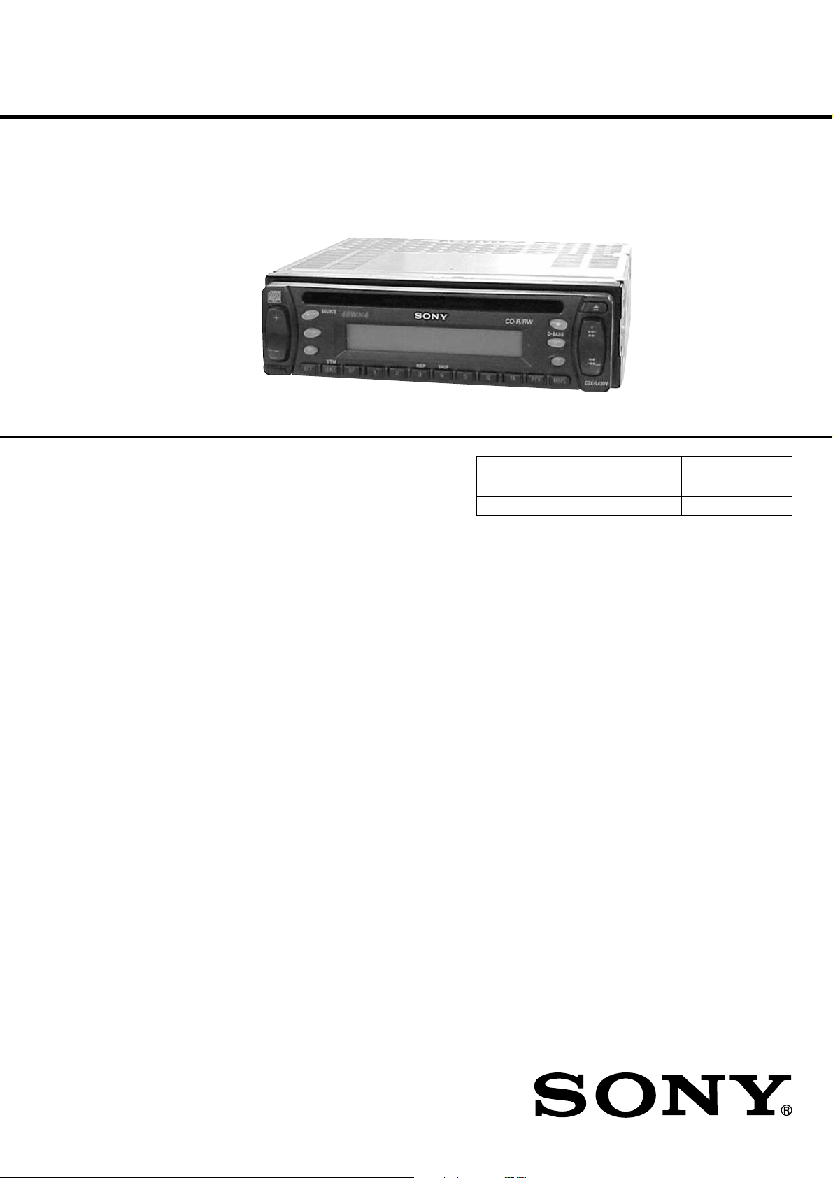
CDX-L420V
SERVICE MANUAL
Ver 1.0 2002. 01
• The tuner and CD sections have no adjustments.
SPECIFICATIONS
AEP Model
UK Model
Model Name Using Similar Mechanism CDX-L410
CD Drive Mechanism Type MG-393XA-121//Q
Optical Pick-up Name KSS-720A
CD player section
Signal-to-noise ratio 90 dB
Frequency response 10 – 20,000 Hz
Wow and flutter Below measurable limit
Tuner section
FM
Tuning range 87.5 – 108.0 MHz
Aerial terminal External aerial connector
Intermediate frequency 10.7 MHz/450 kHz
Usable sensitivity 8 dBf
Selectivity 75 dB at 400 kHz
Signal-to-noise ratio 66 dB (stereo),
72 dB (mono)
Harmonic distortion at 1 kHz
0.6% (stereo),
0.3% (mono)
Separation 35 dB at 1 kHz
Frequency response 30 – 15,000 Hz
MW/LW
Tuning range MW: 531 – 1,602 kHz
LW: 153 – 279 kHz
Aerial terminal External aerial connector
Intermediate frequency 10.7 MHz/450 kHz
Sensitivity MW: 30 µV
LW: 40 µV
Power amplifier section
Outputs Speaker outputs
(sure seal connectors)
Speaker impedance 4 – 8 ohms
Maximum power output 45 W × 4 (at 4 ohms)
General
Outputs Power aerial relay control
lead
Inputs Telephone ATT control lead
Tone controls Bass ±9 dB at 100 Hz
Treble ±9 dB at 10 kHz
Power requirements 12 V DC car battery
(negative ground)
Dimensions Approx. 178 × 50 × 177 mm
(w/h/d)
Mounting dimension Approx. 182 × 53 × 162 mm
(w/h/d)
Mass Approx. 1.2 kg
Supplied accessories Parts for installation and
connections (1 set)
Front panel case (1)
Design and specifications are subject to change without
notice.
9-873-466-01
2002A0400-1
© 2002. 01
FM/MW/LW COMPACT DISC PLAYER
Sony Corporation
e Vehicle Company
Published by Sony Engineering Corporation
1
Page 2
CDX-L420V
SERVICE NOTES
CLASS 1
LASER PRODUCT
This label is located on the bottom of the chassis.
INVISIBLE LASER RADIATION WHEN OPENCAUTION
DO NOT STARE INTO BEAM OR
VIEW DIRECTLY WITH OPTICAL INSTRUMENTS
This label is located on the drive unit’s internal chassis.
When replacing the chassis (T.U) of mechanism deck which have
the “CAUTION LABEL” attached, please be sure to put a new
LABEL (OP CAUTION) (3-223-913-01) to the chassis (T.U).
NOTES ON HANDLING THE OPTICAL PICK-UP BLOCK
OR BASE UNIT
The laser diode in the optical pick-up block may suffer electrostatic
breakdown because of the potential difference generated by the
charged electrostatic load, etc. on clothing and the human body.
During repair, pay attention to electrostatic breakdown and also use
the procedure in the printed matter which is included in the repair
parts.
The flexible board is easily damaged and should be handled with
care.
TEST DISCS
This set can playback CD-R and CD-ROM discs. The following
test discs should be used to check the capability:
CD-R test disc TCD-R082LMT (Part No. J-2501-063-1)
CD-RW test disc TCD-W082L (Part No. J-2501-063-2)
NOTES ON LASER DIODE EMISSION CHECK
The laser beam on this model is concentrated so as to be focused on
the disc reflective surface by the objective lens in the optical pickup block. Therefore, when checking the laser diode emission, observe from more than 30 cm away from the objective lens.
Notes on Chip Component Replacement
• Never reuse a disconnected chip component.
• Notice that the minus side of a tantalum capacitor may be dam-
aged by heat.
SAFETY-RELATED COMPONENT WARNING!!
COMPONENTS IDENTIFIED BY MARK 0 OR DOTTED LINE
WITH MARK 0 ON THE SCHEMATIC DIAGRAMS AND IN
THE PARTS LIST ARE CRITICAL TO SAFE OPERATION.
REPLACE THESE COMPONENTS WITH SONY PARTS WHOSE
PART NUMBERS APPEAR AS SHOWN IN THIS MANUAL OR
IN SUPPLEMENTS PUBLISHED BY SONY.
2
Page 3
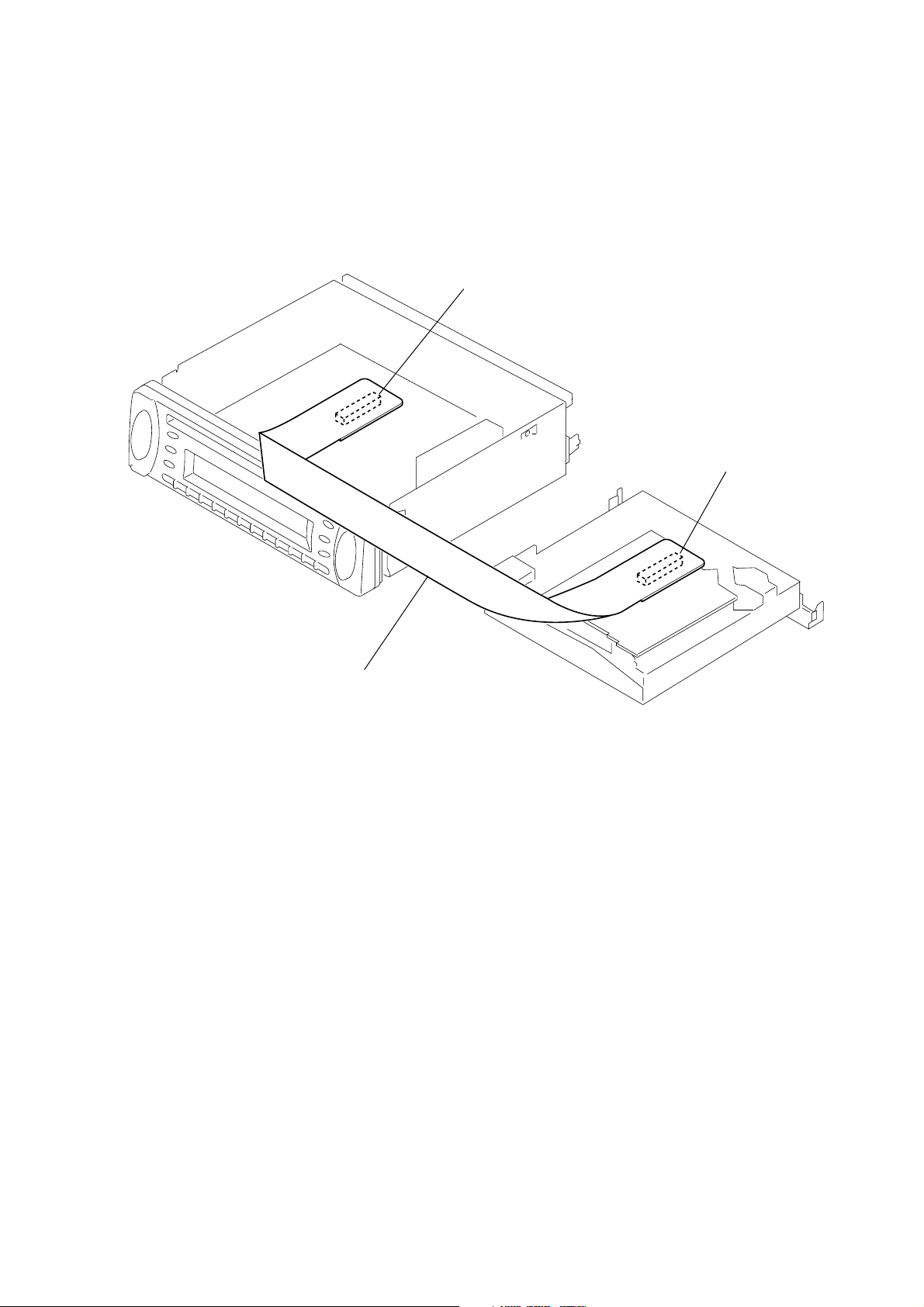
EXTENSION CABLE AND SERVICE POSITION
When repairing or servicing this set, connect the jig (extension cable)
as shown below.
• Connect the MAIN board (CNP301) and the SERVO board (CN1)
with the extension cable (Part No. J-2502-011-1).
CDX-L420V
MAIN BOARD
CNP301
SERVO BOARD
CN1
J-2502-011-1
TABLE OF CONTENTS
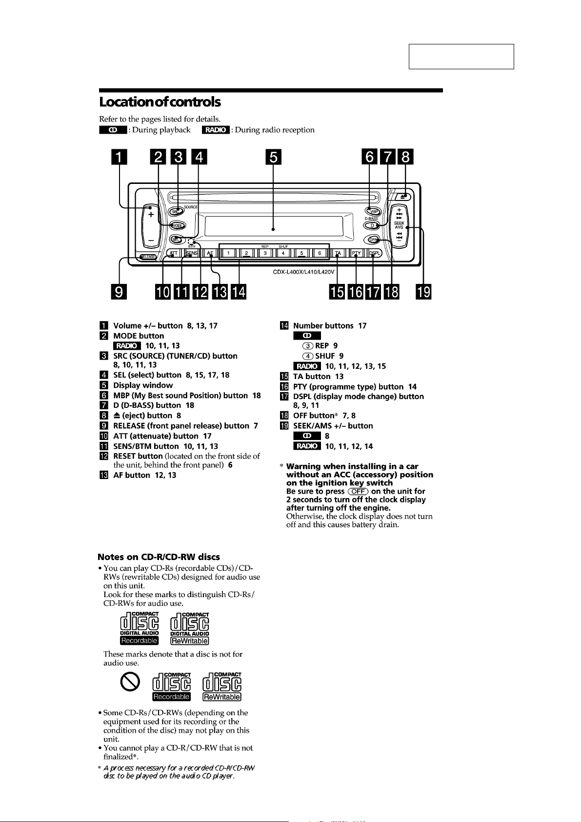
1. GENERAL
Location of controls ................................................................. 4
Notes on CD-R/CD-RW discs ................................................. 4
Connections ............................................................................. 5
2. DISASSEMBLY
2-1. Sub Panel Assy .................................................................... 6
2-2. CD Mechanism Block ......................................................... 7
2-3. Main Board ......................................................................... 7
2-4. Heat Sink ............................................................................. 8
2-5. Chassis (T.U) Assy .............................................................. 8
2-6. Disc in Board ...................................................................... 9
2-7. Servo Board ......................................................................... 9
2-8. Shaft Roller Assy .............................................................. 10
2-9. Floating Block Assy .......................................................... 10
2-10. Optical Pick-up Block ....................................................... 11
3. DIAGRAMS
3-1. IC Pin Description ............................................................. 12
3-2. Circuit Boards Location .................................................... 14
3-3. Block Diagram –CD Section– ........................................... 15
3-4. Block Diagram –Tuner Section– ....................................... 16
3-5. Block Diagram –Display Section– .................................... 17
3-6. Printed Wiring Boards –CD Mechanism Section– ............ 18
3-7. Schematic Diagram –CD Mechanism Section– ................ 20
3-8. Printed Wiring Board –Main Section– .............................. 21
3-9. Schematic Diagram –Main Section (1/2)– ........................ 22
3-10. Schematic Diagram –Main Section (2/2)– ........................ 23
3-11. Printed Wiring Board –Key Section– ................................ 24
3-12. Schematic Diagram –Key Section–................................... 25
4. EXPLODED VIEWS
4-1. Chassis Section ................................................................. 28
4-2. Front panel Section ........................................................... 29
4-3. CD Mechanism Section (1) ............................................... 30
4-4. CD Mechanism Section (2) ............................................... 31
4-5. CD Mechanism Section (3) ............................................... 32
5. ELECTRICAL PARTS LIST......................................... 33
3
Page 4
CDX-L420V
SECTION 1
GENERAL
This section is extracted
from instruction manual.
4
Page 5
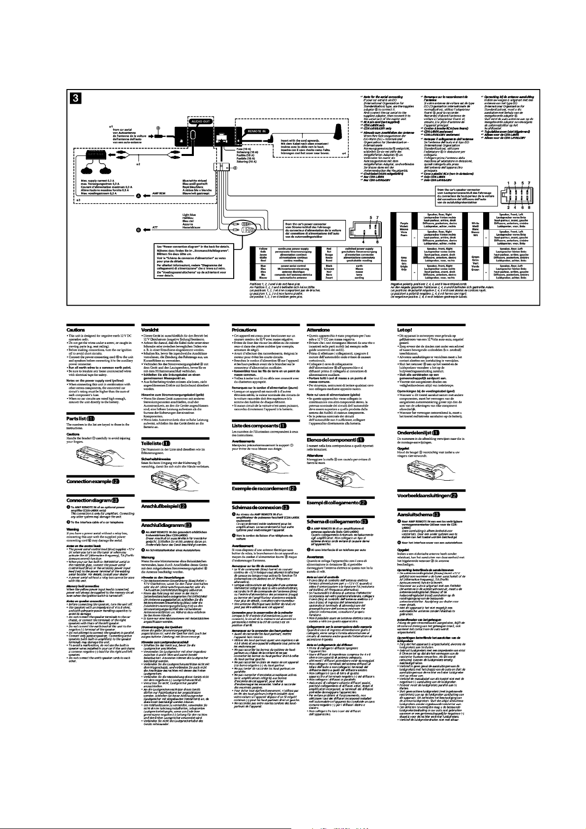
Connections
CDX-L420V
5
Page 6
CDX-L420V
SECTION 2
DISASSEMBLY
Note : This set can be disassemble according to the following sequence.
SET
2-5. CHASSIS (T.U) ASSY
2-1. SUB PANEL ASSY
(Page 6)
(Page 8)
2-2. CD MECHANISM BLOCK
(Page 7)
2-3. MAIN BOARD
(Page 7)
2-4. HEAT SINK
(Page 8)
2-6. DISC IN BOARD
(Page 9)
2-8. SHAFT ROLLER ASSY
(Page 10)
2-9. FLOATING BLOCK ASSY
(Page 10)
2-10. OPTICAL PICK-UP BLOCK
(Page 11)
Note : Follow the disassembly procedure in the numerical order given.
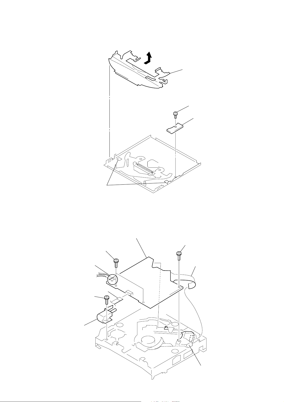
2-1. SUB PANEL ASSY
2-7. SERVO BOARD
(Page 9)
2
PTT 2.6x6
1
PTT 2.6x6
3
claw
5
sub panel assy
4
claws
6
Page 7
2-2. CD MECHANISM BLOCK
6
6
5 CD mechanism block
2 PTT 2.6x6
CDX-L420V
7 bracket (CD)
6 PTT 2.6x
2-3. MAIN BOARD
6 MAIN board
5 ground point screws
(PTT 2.6x6)
3
4 CNP301
4 ground point screw
(PTT 2.6x6)
1 PTT 2.6x6
3 PTT 2.6x
2 PTT 2.6x6
1 PTT 2.6x6
7
Page 8
CDX-L420V
0
y
2-4. HEAT SINK
4 heat sink
3 PTT 2.6x1
2-5. CHASSIS (T.U) ASSY
1
Unsolder the
lead wires.
2
P 2x3
1 PTT 2.6x10
2 PTT 2.6x16
3
P 2x3
4
chassis (T.U) sub ass
black
red
white
8
Page 9
2-6. DISC IN BOARD
4
guide (disc)
1
PS 2x3
2
CDX-L420V
DISC IN board
2-7. SERVO BOARD
2
Removal the solders.
1
MOTOR FLEXIBLE board
3
P 2x3
3
claws
5
PS 2x4
7
SERVO board
6
PS 2x4
8
PICK-UP FLEXIBLE board
4
loading motor assy
optical pick-up block
9
Page 10
CDX-L420V
2-8. SHAFT ROLLER ASSY
• When installing, take note of the positions
arm (roller) and washers. (Fig. 1)
3
retaing ring (roller)
4
bearing (roller)
bearing (roller)
retaing ring (roller)
washer (RA)
arm
Fig. 1
5
shaft roller assy
2
arm (roller T)
washer (RA)
bearing (roller)
arm
2-9. FLOATING BLOCK ASSY
8
compression spring (FL)
1
tension spring (KF1)
1
tension spring (RA3)
7
floating block assy
9
compression spring (FL)
2
tension spring (KR1)
5
Fit lever (D) in the
direction of the arrow.
10
6
Turn loading ring in the
direction of the arrow.
4
damper (T)
3
damper (T)
Page 11
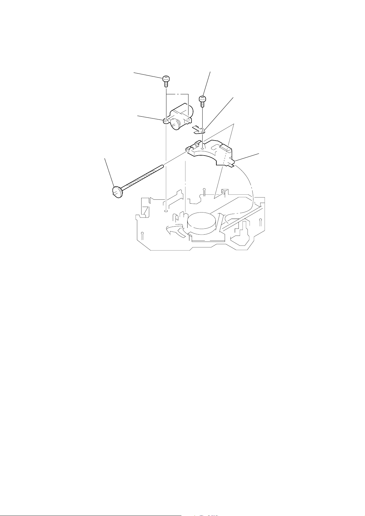
2-10. OPTICAL PICK-UP BLOCK
1
P 2x3
2
sled motor assy
6
shaft (feed) assy
4
P 2x3
5
spring (feed), plate
3
optical pick-up block
CDX-L420V
11
Page 12
CDX-L420V
SECTION 3
DIAGRAMS
3-1. IC PIN DESCRIPTION
• IC501 MN101C49KTD2 (SYSTEM CONTROL)
Pin No. Pin Name I/O Pin Description
1 VREF– — Rated voltage – for A/D converter.
2 VSM I S-meter voltage detection input
3 NC — Not used. (Connect to ground in this set)
4 KEYIN1 I Key input 1
5 KEYIN0 I Key input 0
6 RCIN0 I Rotary commander input 0
7 QUALITY I Noise detection input
8 MPTH I Tuner multi-path detection input
9 NC — Not used. (Connect to ground in this set)
10 VREF+ — Rated voltage + for A/D converter. (+5 V)
11 VDD — Power supply pin (+5 V)
12 OSCOUT O Oscillator output (18.432 MHz)
13 OSCIN I Oscillator input (18.432 MHz)
14 VSS — Ground
15 XIN I Oscillator input (32.768 kHz)
16 XOUT O Oscillator output (32.768 kHz)
17 MMOD — Mode selector (Connect to ground in this set)
18 LCDSO O LCD serial data output
19 LCDCE O LCD chip enable output
20 LCDCKO O LCD serial clock output
21 CD_TSO O CD text serial data output
22 CD_TSI I CD text serial data input
23 CD_TCKO O CD text serial clock output
24 NC — Not used. (Open)
25 NC — Not used. (Open)
26 KEY ACK I Key acknowledge detection input
27 DAVN I RDS data block synchro detection input
28 BUIN I Back-up power detection input
29 NC I Not used. (Connect to ground in this set)
30 CD_SELFSW I CD self switch input
31 CD_PACK I CD pack synchro signal input
32 NC (VCC) — Not used. (Connect to VDD in this set)
33 RESET I Reset input
34 NC — Not used. (Fixed at H in this set)
35 BEEP O Beep output
36 NC — Not used. (Open)
37 TESTIN I Test mode detection input
38 ACCIN I Accessory power detection input
39 NC (VCC) — Not used. (Open)
40 TELATT I Telephone attenuate detection input
41 NC (VCC) — Not used. (Connect to VDD in this set)
42 UNISO O SONY BUS data output
43 UNISI I SONY BUS data input
44 UNICKO O SONY BUS clock output
45 I2C_SIO I/O I2C BUS serial data input/output
46 NC — Not used. (Open)
47 I2C_CKO O I2C BUS serial clock output
48 NC — Not used. (Open)
49 TUNON O Tuner power control output
50 PW_ON O System power control output
51 TSTB O CD text strobe output
12
Page 13

Pin No. Pin Name I/O Pin Description
52 RFOK I CD RFOK signal input
53 CD_RST O CD reset signal output
54 A0 O CD command/parameter signal output
55 STB O CD strobe signal output
56 X_EN O CD crystal oscillator control output (Not used in this set)
57 LIMIT I CD limit switch input
58 PH1 I Not used. (Fixed at H in this set)
59 D_SW I CD down switch input
60 INSW I CD disc in switch input
61 NC (PH3) — Not used. (Fixed at H in this set)
62 CD_LM_LO O Loading motor control output (Loading direction)
63 CD_LM_EJ O Loading motor control output (Eject direction)
64 NC — Not used. (Open)
65 NC — Not used. (Open)
66 AMPATT O Power amplifier attenuator control output
67 AMPON O Power amplifier standby control output
68 CDMD_ON O CD mechanism power control output
69 ATT O System attenuate control output
70 VOLATT O Electronic volume attenuate control output
71 NC — Not used. (Open)
72 NC — Not used. (Open)
73 NC — Not used. (Open)
74 NC — Not used. (Open)
75 NC — Not used. (Open)
76 NC — Not used. (Connect to ground in this set)
77 NC — Not used. (Connect to ground in this set)
78 DIMSEL — Not used. (Open)
79 XCD_ON O CD power control output
80 TU-ATT — Not used. (Open)
81 NC — Not used. (Open)
82 NC — Not used. (Open)
83 NC — Not used. (Open)
84 NC — Not used. (Open)
85 NC — Not used. (Open)
86 E2P_SIO I/O EEPROM serial data input/output
87 E2P_CKO O EEPROM serial clock output
88 NC — Not used. (Open)
89 FLASH_W I Flash write input
90 NS_MASK O Noise detection output
91 AD_ON O Key power control output
92 NC — Not used. (Open)
93 ILLON O Illumination power control output
94 DOORSW I Not used. (Connect to ground in this set)
95 DAVSS — Ground for D/A converter.
96 NC — Not used. (Open)
97 NC — Not used. (Open)
98 RCIN1 I Rotary commander input 1
99 RAMBU — Not used. (Connect to ground in this set)
100 DAVDD — D/A converter power supply pin (+5 V)
CDX-L420V
13
Page 14

CDX-L420V
3-2. CIRCUIT BOARDS LOCATION
DISC IN board
KEY board
SUB board
LIMIT board
tuner unit
(TU10)
MAIN board
SERVO board
• Waveforms — Servo Board —
(MODE: CD PLAY)
1
16.9344MHz
wd
(XTAL)
IC1
2
3.4msec
IC1
(PACK)
ts
3
uj
(RFO)
IC1
4
2.4Vp-p
4.8Vp-p
1.8Vp-p
0V
— Main Board —
1
4.332MHz
IC51
(OSCO)
4
2
18.432MHz
IC501 qs (OSCOUT)
3
32.768kHz
IC501
(XOUT)
qh
5.2Vp-p
3.6Vp-p
5.2Vp-p
14
5
Approx. 620mVp-p
IC1
IC1
(FEO)
oa
Approx. 200mVp-p
(TEO)
od
0V
Page 15

3-3. BLOCK DIAGRAM — CD SECTION —
OPTICAL PICK-UP
(KSS-720A)
RF AMP,DIGITAL SERVO,
DIGITAL SIGNAL PROCESSOR
IC1
CDX-L420V
PD
LD
A
C
B
D
E
F
FOCUS
COIL
I-V
CONV.
LD
DRIVE
Q1
A
84
C
85
B
82
D
83
E
87
F
86
PD
97
LD
98
FOCUS/TRACKING COIL DRIVE,
SLED/SPINDLE/LOADING MOTOR DRIVE
FSC
15
FSC
16
TRACKING
ERROR
LD AMP
IC2
+
FOCUS
COIL
DRIVE
FD
26
FORCUS
ERROR
RF
EQ
EFM
DEMOD
SERVO
CTL
FDTDSD
62 63 64 65
MD
D/A
CONV
DSUB CODE
PROCESS
I/F
OSC
23 24
X1
16.9344MHz
LOUT
ROUT
TSCK
PACK
TSTB
TSI
SCK
STB
RST
RFOK
XTALEN
(Page 16)
TUNER
SECTION
16
12
R-CH
55
52
56
54
SI
8
SO
7
6
5
AO
4
3
2
9
SW1
(DISC IN)
CDL
A
SYSTEM CONTROL
CD PACK
31
TSTB
51
21
CD TSO
22
CD TSI
23
CD TCKO
55
STB
54
AO
53
CD RST
52
RFOK
60
IN SW
IC501 (1/3)
TRACKING
COIL
M902
(SLED)
M901
(SPINDLE)
M903
(LOADING)
17
18
+-
M
13
14
+-
M
11
12
+-
M
9
10
TRK
TRK
SL-
SL+
SP-
SP+
LD-
LD+
+
-
TRACKING
COIL
DRIVE
SLED
MOTOR
DRIVE
SPINDLE
MOTOR
DRIVE
LOADING
MOTOR
DRIVE
SD
MD
LOAD
EJECT
30
SW2
POWER
CONTROL
Q332
BATT
(SELF)
SW3
(LIMIT)
SW5
(DOWN)
POWER
CONTROL
Q333
TD
23
5
6
1
2
A5V
AU5V
D5V
DR6V
REG
Q341
REG
Q331
CD SELF SW
LIMIT
57
59
D SW
CD LM LO
62
63
CD LM EJ
68
CDMD ON
XCD ON
79
RESET
IC602
33
1
S702
RESET
RESET
BU 5V
3
Signal path
: CD
R-ch is omitted due to same as L-ch.
15 15
Page 16

CDX-L420V
3-4. BLOCK DIAGRAM — TUNER SECTION —
J10
(ANTENNA)
TUNER UNIT
TU10
ANTFM MPX
2 10
ANTAM
1
AM DET
S-METER
I2C SDA
I2C SCL
RDS DET
8
14
12
13
9
FM BUFFER
Q21
NOISE
6 1
SUPPRESSOR
9
SDA SCL
LV IN
20 2
MPX
16
(Page 15)
SECTION
IC20
Q22
NOISE
SUPPRESSOR
ON
10
MULTI
PATH
DET
RDS/RDBS
DEM/DEC
CD
A
CDL
RDS DECODER
IC51
8
ELECTRONIC VOLUME
IC401
SE L
1
MPX
13
AM
11
LEVEL
14
MPIN
15
SDA
20
SCL
21
SM
18
SYSTEM CONTROL
IC501 (2/3)
VOL ATT
70
QUALITY
7
NS MASK
90
VSM
2
I2C SIO
45
I2C CKO
47
MPTH
8
DAVN
27
OUT FL
OUT RL
ATT
BEEP
AMP ON
AMP ATT
TEL ATT
ACC IN
TEST IN
TUN ON
PW ON
POWER AMP
IC404
30
29
Q451
MUTE
Q478,479
69
35
67
66
40
38
37
49
50
MUTE
CONT
Q431
MUTE
BATT
CHECK
Q631
POWER SUPPLY
7
VCC
2
8.7V ON
3
5.6V ON
4
STB
ACC
IC601
12
11
AUX
16
STBY
4
MUTE
22
TEL
ATT
Q651
8
ANT+B
5
BU+B BU 5V
9
COM 8V
10
TU 5.6V
11
TU 8.7V
5
3
9
7
R-CH
BATT
COM 8V
TU 5.6V
TU 8.7V
F901
CNP601
10
12
11
16
13
15
1
FL+
9
FL
2
RL+
RL
4
FR+
FR
3
RR+
RR
BATT
ATT
7
ACC
TEST (NC)
6
ANT REM
-
-
-
-
E2PROM SDA
E2PROM SCL
OSCO OSCI
4 5
17
18
X51
4.332MHz
86
87
E2P SIO
E2P CKO
BU IN
BATT DET
Q556
BATT DET
28
Q551,557
BATT
BATT
Signal path
: FM
: MW
: CD
R-ch is omitted due to same as L-ch.
1616
Page 17

3-5. BLOCK DIAGRAM — DISPLAY SECTION —
CDX-L420V
KEY MATRIX
LSW900-922
J561
(REMOTE IN)
KEY
ACTIVE
Q664
X502
32.768kHz
SYSTEM CONTROL
IC501 (3/3)
KEY IN0
5
KEY IN1
KEY ACK
26
AD ON
91
RC IN1
98
RC IN0
6
XIN
15
XOUT
16
LCD SO
LCD CKO
LCD CE
ILL ON
OSC OUT
OSC IN
LCD DRIVE
IC901
18
20
194
93
12
13
64
63
62
BATT
X501
18.432MHz
DI
CL
CE
POWER
CONT
Q661,662
LCD901
PL901,902
ILL +B
LED921,922
17 17
Page 18

CDX-L420V
3-6. PRINTED WIRING BOARDS — CD MECHANISM SECTION — • Refer to page 14 for Circuit Boards Location.
THIS NOTE IS COMMON FOR PRINTED WIRING
BOARDS AND SCHEMATIC DIAGRAMS.
(In addition to this, the necessary note is
printed in each block.)
for schematic diagram:
• All capacitors are in µF unless otherwise noted. pF: µµF
50 WV or less are not indicated except for electrolytics
and tantalums.
• All resistors are in Ω and 1/
specified.
• % : indicates tolerance.
f
•
• C : panel designation.
Note: The components identified by mark 0 or dotted line
• A : B+ Line.
• Power voltage is dc 14.4V and fed with regulated dc power
• Voltages are taken with a VOM (Input impedance 10 MΩ).
• Waveforms are taken with a oscilloscope.
• Circled numbers refer to waveforms.
• Signal path.
: internal component.
with mark 0 are critical for safety.
Replace only with part number specified.
supply from ACC and BATT cords.
Voltage variations may be noted due to normal production tolerances.
Voltage variations may be noted due to normal production tolerances.
F : FM
f : MW
J : CD
4
W or less unless otherwise
234567891011121314
1
A
B
C
D
E
for printed wiring boards:
• X : par ts extracted from the component side.
• Y : par ts extracted from the conductor side.
a
•
• : Pattern from the side which enables seeing.
Caution:
Pattern face side: Parts on the pattern face side seen from the
(Side B) pattern face are indicated.
Parts face side: Parts on the parts face side seen from the
(Side A) parts face are indicated.
: Through hole.
(The other layer’s patterns are not indicated.)
F
G
H
SW5
I
J
1818
Page 19

CDX-L420V
A
B
C
D
E
F
G
H
1
M903
234567891011121314
• Semiconductor
Location
Ref. No. Location
IC1 E-7
IC2 H-7
Q1 C-6
TP66
TP73
TP53
TP64
TP86
TP87
TP75
TP47
TP69
TP57
R21
TP48
TP68
TP54
R22
TP56
TP76
R20
TP52
TP74
FB5
C71
TP50
TP58
TP61
C44
TP51
R31
TP62
TP85
CN1
TP49
TP7
TP91
TP19
CN3
TP90
TP80
TP60
TP59
TP72
C26
TP77
TP63
R26
TP71
R19
C4
R17
TP55
TP9
TP8
TP78
TP20
TP70
C27
C6
R30
Q1
X1
R3
C25
C34
R18
C41
TP17
C3
R6
R7
TP79
C29
TP92
TP16
C5
C17
C22
C1
R29
TP11
C16
C36
C9
C8
C10
TP34
TP35
C43
TP12
C70
TP36
C15
IC1
TP46
C38
IC2
TP82
TP39
BP2
TP81
TP37
TP38
TP41
BP1
C11
TP42
TP31
TP40
TP30
TP83
C14
TP45
TP27
C13
TP44
TP43
R12
R10
TP26
C30
TP28
C18
R9
C24
TP23
TP33
TP29
R5
TP89
C35
TP32
R15
TP84
TP10
C19
TP88
TP15
BP3
TP4
TP6
TP3
TP2
C20
R8
R14
TP22
TP24
TP25
TP14
BP4
TP18
TP21
(Page 21)
C23
SW3
SW1
SW2
TP1
TP5
CN1
I
M902
M901
J
19 19
Page 20

CDX-L420V
3-7. SCHEMATIC DIAGRAM — CD MECHANISM SECTION —• Refer to page 26 for IC Block Diagrams.
• Refer to page 14 for Waveforms and page 18 for Common Note on Schematic Diagram.
SW3
M902
M901
SW1
SW2
CN1
CN3
TP5
TP2
TP3
M903
TP77
TP78
C1
TP81
TP82
TP83
TP84
SW5
C5
R29
R30
TP79
TP80
C43
TP1
TP4
TP92
TP85
TP87
TP86
Q1
TP9 TP8
R26
R3
C4
C3
TP7
C6
C14
TP10
C13
C11
R5
C15
C10
TP12
C9
TP11
C8
C16
C70
TP89
IC B/D
R7
TP21
TP15
BP3
C22
TP18
TP14
BP4
R6
TP17
TP20
TP16
TP19
C17
C18
C19
C20 C23
R9
C24
C35
C36
TP45
TP44
TP43
TP42
TP41
TP40
TP39
TP38
TP37
TP46
TP36
TP35
TP34
C44
R31
C38
FB5
TP6
R22
R21
R18
R19
R20
R17
TP66
TP61
TP76
TP60
TP75
TP59
TP74
TP58
TP73
TP57
TP72
TP56
TP71
TP55
TP70
TP54
TP69
TP53
TP68
TP52
TP51
TP50
TP64
TP49
TP48
TP63
TP47
TP62
CN1
(Page 22)
IC1
R12
R10
C30
C26
C27
TP31
BP1
TP30
R15
R14
TP90
TP91
TP27
TP29
TP26
TP28
TP88
C29
C25
C34
X1
C71
TP33
BP2
TP32
TP24
TP25
TP22
TP23
R8
C41
IC2
IC B/D
Note:
• Voltage is dc with respect to
ground under no-signal conditions.
no mark : CD PLAY
2020
Page 21

3-8. PRINTED WIRING BOARD — MAIN SECTION — • Refer to page 14 for Circuit Boards Location and page 18 for Common Note on Printed Wiring Boards.
CDX-L420V
A
B
C
D
E
F
G
H
1
C804
JW2
C59
Q21
C21
C22
C23
R22
C25
C801
R26
I
23456789101112131415
J561
J10
JW75
C343
C505
C502
CNP601
C617
D614
JW76
C301
JW80
C504
F901
JW81
R506
R505
R504
C511
JW127
JW126
JW119
JW73
JW82
C503
R631
JW88
R636
JW112
C506
JW84
JW103
C510
R632
JW92
JW113
JW85
C805
R557
JW105
R609
D609
JW117
JW118
JW89
JW90
JW91
JW114
R507
JW102
Q557
R555
Q664
JW104
JW94
JW100
C622
R503
JW86
JW87
JW144
JW97
JW98
JW99
JW95
R524
IC602
JW116
D601
Q551
JW142
JW110
JW115
C602
JW108
C613
D331
JW106
JW160
Q556
C611
R342
D621
JW101
JW107
Q332
C331
JW161
C601
C614
Q341
R661
R672
R674
D551
JW109
C612
R341
R331
Q662
R556
D613
R332
JW140
JW141
D556
R551
IC601
Q331
R333
Q661
R662
R663
R664
R665
L500
JW96
R334
R660
R673
R671
JW139
JW111
(Page 19)
• Semiconductor Location
Ref. No. Location
D21 H-3
D22 H-3
D23 G-3
D331 I-10
D332 H-6
D341 F-7
D471 B-7
D472 B-7
D473 C-7
D474 C-7
D475 C-6
D476 C-6
D477 C-5
D478 C-5
D479 D-6
D480 D-6
D551 C-10
D556 D-10
D601 C-9
D609 C-9
D610 D-6
D613 E-10
D614 D-8
D621 G-10
D651 D-7
D671 I-5
D701 I-3
D710 I-2
D711 I-2
D715 I-4
D716 I-2
Ref. No. Location
D717 I-2
D718 I-2
IC20 H-2
IC51 G-4
IC401 E-3
IC404 B-6
IC501 H-7
IC601 E-10
IC602 H-9
Q21 G-1
Q22 H-3
Q331 F-10
Q332 H-10
Q333 H-6
Q341 F-10
Q431 C-4
Q441 C-4
Q451 C-3
Q461 C-3
Q478 D-6
Q479 C-6
Q551 G-9
Q556 D-10
Q557 H-9
Q631 D-8
Q651 D-7
Q661 H-10
Q662 I-10
Q664 I-9
TU10
C31
R31
C32
C33
C41
C42
R21
C17
JW9
C24
R24
R25
C11
C15
JW7
IC20
D718
D717
D710
JW1
JW10
C29
C26
R27
C14
R32
R41
JW11
R29
R28
C28
D716
D711
JW8
C16
C27
JW6
D23
C431
JW3
JW4
JW13
D22
D21
JW138
C405
C412
C411
C403
JW137
Q461
C451
JW35
JW17
R711
R710
D701
JW136
CN701
C406
JW18
C63
Q22
JW135
R431
JW132
R451
C441
JW36
JW158
C62
JW134
R462
Q451
JW14
IC401
R403
R60
C58
JW133
R461
C61
R519
R702
R701
C661
R452
JW131
R441
C461
R434
R454
R56
C56
D715
R432
Q431
JW15
JW16
JW47
R464
R444
C404
IC51
R52
JW43
JW130
Q441
R453
R463
C401
JW32
C54
R54
R53
C53
JW44
R433
R443
JW33
R57
C55
C52
C475
R442
C402
JW34
JW45
C51
C803
JW23
JW46
JW48
C433
C442
C453
C463
JW25
JW26
JW24
JW27
C64
JW38
C57
X51
JW41
JW42
JW68
R475
JW28
JW29
JW30
JW39
JW40
R522
R501
D477
C471
R508
R529
R530
C529
D671
JW20
JW49
JW50
JW51
JW52
JW53
JW54
R471
JW64
JW55
C474
R472
C303
JW143
JW66
JW63
JW21
JW56
D478
Q479
R474
C472
JW57
D610
JW60
JW61
JW59
JW67
IC404
Q478
D332
JW62
JW58
R517
R516
JW65
JW156
D476
C479
C480
R515
Q333
JW69
JW151
JW152
JW153
JW154
JW155
D475
R473
R479
D480
D479
CNP301
JW70
JW22
D473
C473
R653
R480
C501
JW157
R651
D651
R652
C332
R514
R520 R521
JW129
C302
C305
C341
R510
JW128
D472
D471
D474
C631
R654
Q651
R525
R511
R512
IC501
C477
JW120
R634
C342
JW121
JW83
JW125
R633
R637
R528
R526R527
D341
JW123
Q631
JW77
JW78
R502
JW124
JW122
JW79
X502
X501
S702
J
(Page 24)
21 21
Page 22

CDX-L420V
• Refer to page 14 for Waveforms and page 18 for Common Note on Schematic Diagram.
3-9. SCHEMATIC DIAGRAM — MAIN SECTION (1/2) —• Refer to page 26 for IC Block Diagrams.
C42
IC20
R32
R26
C33
R27 C27
C26
D21
D22 R29
C28 R28
D23
C801
Q22
C411
C412
IC B/D
R403
C406
C403 C404
IC401
C405
C402
C401
R434
R454
R444
R464
J10
TU10
C17
C11
C15
C16
C14
C63
C62
C61
C59
C58
R60
R56
Q21
C51
C64
R21
C41
R31
C22
R22
C23
C21
C31 C32
R41
C25
R25
C24 C29
R24
IC B/D
IC51
R52
C52
R53
C53
R54
C54
X51
C55
C56
C57
R57
R508
C803
C302
JW76
C305
C301
Q341
R342
R341
C343
C342
D341
Note:
• Voltage is dc with respect to ground under no-signal
(detuned) condition.
no mark : FM
( ) : MW
< > : CD PLAY
C341
C332
CNP301
R334
R331
R332
R333
C331
Q331
(Page 20)
Q332
D332
D331
C303
Q333
R512
R514
R515
R516
R517
C529
R529
R524
R530
IC501
R519
R503
C506
R522
R525
R527R526
R528
R507
R502
R510
R511
X502
X501
Q664
C510
C511
R506
R505
R504
C505
C504
C503
C502
(Page 23)
R520
R521
R501C501
2222
Page 23

3-10. SCHEMATIC DIAGRAM — MAIN SECTION (2/2) — • Refer to page 18 for Common Note on Schematic Diagram and page 26 for IC Block Diagrams.
CDX-L420V
C431
C451
C461
C441
R431
R451
R461
R441
R432
R452
R462
R442
Q479
Q478
Q431
Q451
Q461
Q441
D479
C480
C479
R479
D480
R433 C433
R463 C463
R443 C442
C471
R480
C472
R472
C453R453
R475
R471
C473
IC601
IC404
R474R473
C474
C475
C477
D471
D472
D473
D474
D475
D476
D477
D478
C602
C601
D609
D601
R609
C617
L500
CNP601
F901
C804
IC B/D
(Page
22)
IC602
R636
R637
R557 R555
Q557
C805
Q631
R634
R633
D610
C622
Q551
C631
Q556
D621
R632
D551
D556
R631
C611
R551
R556
C612 C613 C614
C661
R662
R663
R664
R665
Q651
D613
R654
Q662
R660
R653
Q661
D614
R661
R652
D651
R651
D715
D701
D671
R710
R711
R702
R701
R671
S702
R672
D710
R673
D711
D718
R674
D717
CN701
(Page 25)
D716
J561
Note:
• Voltage is dc with respect to ground under no-signal
(detuned) condition.
no mark : FM
23 23
Page 24

CDX-L420V
3-11. PRINTED WIRING BOARD — KEY SECTION — • Refer to page 14 for Circuit Boards Location and page 18 for Common Note on Printed Wiring Boards.
A
B
C
D
1
LSW903
LSW904
2 3 4 5 6 7 8 9 10 11 12 13 14 15
LED921
LSW902
LSW905
LSW906
LSW907 LSW908 LSW909
LED931
LED941
LED932
LCD901
LED942
LSW920LSW921LSW922
LED922
LSW900
LSW912
LSW911
LSW913
LSW901
LSW910
LSW914LSW915LSW916LSW917LSW918LSW919
E
F
G
H
(Page 21)
R953
R963
R973
R983
R982
R981
R903
R904
R951
R906
R905
R976
R908
R971
R907
R961
R966
R909
R956
R937
R936
R935
R932
R933
R934
R955
R965
R975
R921
R920
R919
R949
IC901
R948
R947
R918
R917
C992
R916
C993
R974
C991
R964
R954
R994
C994
R995
D991
R993
C995
R992
R991
R997
D902
R998
R996
R990
CN901
R902
R901
R972
R977
R967
R962
R985
R911
R915
R912
R952
R957
R984
R914
R913
R910
• Semiconductor
Location
I
Ref. No. Location
(D902) H-11
(D991) G-10
(IC901) G-8
LED921 A-2
LED922 A-13
LED931 B-4
LED932 B-11
LED941 C-4
LED942 C-11
( ) : SIDE B
2424
Page 25

3-12. SCHEMATIC DIAGRAM — KEY SECTION — • Refer to page 18 for Common Note on Schematic Diagram.
CDX-L420V
(Page 23)
CN901
R934
R935
R936
LED921
LED922
LED942
R937
R933
R932
R996
R997
R998
LED931 LED941
D902
LED932
LSW910 LSW911 LSW912 LSW913 LSW914
R983
R981
R982
LSW903
R951
R961
R971
LSW904
LSW910
LSW911
R952
LSW915 LSW916 LSW917 LSW918 LSW919 LSW920 LSW921 LSW922
R962
R972
LSW902
LSW901
LSW906
LSW905
R953
R963
R973
LSW914
LSW915
LSW916
LSW917
R954
R917R916R915R914R913R912R911R910
R964
R974
R918
R955
LSW921
LSW920
LSW919
LSW918
R965
R975
R956
LSW907
LSW908
LSW909
LSW922
R966
R976
R921R920R919
LSW913
LSW912
LSW900
R957
R984
R967
R985
R977
D991
R990
R994
C994
R991
R993
C991
R995
C995
R992
C992
C993
R947
R948
R949
IC901
LSW900
R901 R902 R903 R904 R906 R907
LSW901 LSW902 LSW903 LSW904 LSW905 LSW906 LSW907 LSW908
R905
R908
R909
LSW909
LCD901
Note:
• Voltage is dc with respect to ground under no-signal
(detuned) condition.
no mark : FM
25 25
Page 26

CDX-L420V
• IC Block Diagrams
IC1 µPD63711GC-8EU
AGCO74RFI73C3T72ASY71EFM70AVDD697E DAC3687D DAC2677C DAC1667F DAC065MD64SD63TD62FD
75
AGCI
76
RFO
77
EQ2
78
EQ1
79
RF-
80
AGND
81
A
82
C
83
B
84
D
AVDD
REFOUT
FEO
TE-
TEO
TE2
TEC
AGND
AVDD
85
F
86
E
87
88
89
FE-
90
91
92
93
94
95
96
PD
97
LD
98
99
PN
100
AMP BLOCK
DEFECT
MIRR
EFM
COMPARATOR
EFM
FEOFS
TEOFS
RF
EFM
SWITCH
FOK
A3T
FEO
TEO
COMPARATOR
MICROCOMPUTER INTERFACE
AUTO GAIN
CONTROLLER
SVDRAM
PROCESSOR
DEFECT
COMPARATOR
RFENV
MIRENV
TRACKING
A/D CONVERTER
REGISTER
FOCUS
REGISTER
D/A
ADDER
MULTIPLIER
SVROM
CLV
FD/TD/SD/MD
CONTROLLER
SVCRAM
ROM
DECODER
ATEST59TEST158TEST057DGND56TSTB55TSCK54TSI53TSO52PACK51DVDD
AGND
60
61
MICROCOMPUTER INTERFACE
CD-TEXT DECODER
MEMORY
PROCESSOR
16K
SRAM
SUB-CODE PROCESSOR
EFM DEMODULATOR
TIMING GENERATOR
D/A
INTERFACE
CIRCUIT
DE-EMPHASIS CIRCUIT
OCTUPLED
OVERSAMPLING DIGITAL FILTER
NOISE SHAVER
OUTPUT BUFFER
SCF
NOISE SHAVER
OUTPUT BUFFER
OSC
DIGITAL PLL
DIGITAL
AUDIO
INTERFACE
OUTPUT PROCESSOR
ERROR
PROCESSOR
CORRECTION
C2D3
50
C2D2
49
C2D1
48
C1D2
47
C1D1
46
DGND
45
PLCK
44
MIRR/WFCK
43
RFCK
42
LOCK
41
DVDD
40
TSOI
39
C16M
38
DGND
37
TX
36
HOLD/WDCK
35
LRCK
34
LRCKIN
33
SCKO
32
SCKIN
31
DOUT
30
DIN
29
FLAG
28
EMPH
27
DVDD
26
FWD
REV
LDCONT
IN1
IN2
PREVCC
POWVCC
VOL–
VOL+
VO2–
VO2+
VO1–
VO1+
IC2 BA5810FP-E2
1
2
X3
3
PS
4
5
6
7
8
9
10
10k
11
12
10k
10k
13
14
10k
POWER
PREVCC
(PRE.LOADING)
POWVCC12
(CH1.CH2)
–
+
+
–
–
+
+
–
SAVE
10k
10k
10k
10k
LOADING PRE
7.5k
–
16k
LEVEL
SHIFT
FWD REV
7.5k
16k
+
LEVEL
SHIFT
BIAS
28
+
–
+
7.5k
–
+
–
+
–
16k
27
26
25
24
23
22
OPIN4+
OPIN4–
OPOUT4
OPIN3+
OPIN3–
OPOUT3
7.5k
LEVEL
SHIFT
–
+
LEVEL
SHIFT
CH1-4
MUTE
16k
POWVCC34
(CH3,CH4)
10k
10k
10k
10k
–
+
+
–
–
+
+
–
10k
10k
10k
10k
21
20
19
18
17
16
15
MUTE
POWVCC
GND
VO3–
VO3+
VO4–
VO4+
1
2
3
RST
RFOK
DGND
IC51 SAA6588T
CIN
LVIN
20
19
MULTI
PATH
DETECTOR
CLOCKED
COMPARATOR
RDS/RDBS
DEMODULATOR
OSCILLATOR
TEST
CONTROL
2
1
3
MRO
TCON
MPTH
4A05
SCOUT
18
BAND-PASS FILTER
RDS/RDBS
DECODER
& CLOCK
4 5
OSCI
OSCO
6
STB
SCK
57kHz
8th ORDER
6
7SO8SI9
CLOCK
DATA
7
VSSD
VDDD
XTALEN
VREF
17
SIGNAL QUALITY
DECODER
445
INTERFACE
REGISTER
8
DAVN
10
DVDD
VSSA
MPX
15
POWER SUPPLY
& RESET
11
DAVDD
12
ROUT
VDDA
14
CLOCK
DATA
IIC BUS SLAVE
TRANSCEIVER
9 10
13
1316
SDA
DAGND
AFIN
SCL
1514
REGC
DAGND
PAUSE
DETECTOR
16
17
18R+19R–20L+21L–22
LOUT
DAVDD
MAD
PSWN
11
12
23
XVDD
XTAL24XTAL
25
XGND
IC601 BA4908-V3
–
+
2 3
4
1
NC
STB
MODE2
MODE1
REGULATOR
OVER VOLTAGE
PROTECT
5 6 7 8 9
ANT
VCC
VDD
AMP
COM
–
+
10
AM
–
+
11
FM
–
+
12
GND
2626
Page 27

IC401 TDA7402TR
ACINLR
ACINLR
ACINRR
OUTLF
33
OUTLR
OUTRF
28 2730 2932 31
OUTRR
OUTSWL
OUTSWR
26 25 24 23
OUTSSL
CDX-L420V
OUTSSR
ACINLF
SWINR
SWINL
AC OUTR
AC OUTL
VREF
MUX
MD1 (SE4L)
MD1G (SE4R)
MD2
MD2G
MONO
FADER
MIXER
MIXING
SUBWOOFER
+PHASE
CONTROL
SECOND SOURCE
LOUDNESS
IN GAIN
MUTE
SELECTOR
II
C-BUS
DIGITAL
CONTROL
BEEP
HIGH OUT
S & H
LP
DEMODULATOR
+STEREO ADJUST
+STEREO BLAND
PILOT
CANCELLATION
LP
PIL, DET
PLL
QUAL.
MALTI
PATH
DETECTOR
MONO
FADER
34
35
36
37
38
LP
HP
BASS
39
40
41
42
43
44
TRABLE
VOLUME
SOFT MUTE
LOUDNESS COMPANDER
IN GAIN
+ AUTO
ZERO
MAIN SOURCE
SELECTOR
OUTPUT CONTROL
VOICE
BANDPASS
INPUT MULTIPLEXER
MONO
FADER
SELECTOR
SUPPLY
D/A
PULSE
FORMER
AM/FM
NOISE
BLANKER
22
21
20
19
18
17
16
15
14
13
12
VDD
SCL
SDA
GND
MUTE
QUAL
MP OUT
MP IN
LEVEL
MPX
AMIF
1 2 3 4 5 6 7 8 9 10 11
CD L
CD R
SE2L
SE2R
AUX L
AUX R
FD2L+
FD2L–
FD2R+
FD2R–
AM
27
Page 28

CDX-L420V
NOTE:
• The mechanical parts with no reference
number in the exploded views are not supplied.
• Items marked “*” are not stocked since
they are seldom required for routine service.
Some delay should be anticipated
when ordering these items.
• -XX and -X mean standardized parts, so
they may have some difference from the
original one.
4-1. CHASSIS SECTION
5
SECTION 4
EXPLODED VIEWS
• Color Indication of Appearance Parts
Example :
KNOB, BALANCE (WHITE) ... (RED)
• Accessories are given in the last of this parts list.
MG-393XA-121//Q
R
Parts Color Cabinet’s Color
R
6
The components identified by
mark 0 or dotted line with mark.
0 are critical for safety.
Replace only with part number
specified.
TU10
8
#1
#3
#1
#5
13
14
7
#1
#2
#2
#3
12
#1
F901
#1
#11
#2
8
4
10
#4
9
11
#4
#1
3
2
16
#1
1
Ref. No. Part No. Description Remark
1 X-3380-162-4 PANEL SUB ASSY, SUB
2 3-042-244-11 SCREW (T)
3 X-3379-876-3 LOCK ASSY (S)
4 3-223-782-21 COVER
5 1-776-527-82 CORD (WITH CONNECTOR) (ISO) (POWER)
6 3-041-012-11 BRACKET (CD)
7 A-3340-228-A MAIN BOARD, COMPLETE
8 3-376-464-11 SCREW (+PTT 2.6X6), GROUND POINT
* 9 3-225-136-01 HEAT SINK (REG)
* 10 3-225-271-02 CHASSIS (BACK)
* 11 3-040-998-01 BRACKET (IC)
* 12 3-225-135-01 HEAT SINK
28
#1
15
Ref. No. Part No. Description Remark
* 13 3-045-877-02 CUSHION (TU)
* 14 3-045-878-01 PLATE (TU), GROUND
15 3-225-133-11 CHASSIS
16 3-231-821-01 PLATE, INSULATED
F901 1-532-877-11 FUSE (BLADE TYPE) (AUTO FUSE) 10A
TU10 A-3220-812-A TUNER UNIT (TUX-020)
#1 7-685-792-09 SCREW +PTT 2.6X6 (S)
#2 7-685-795-09 SCREW +PTT 2.6X12 (S)
#3 7-685-793-09 SCREW +PTT 2.6X8 (S)
#4 7-685-647-79 SCREW +BVTP 3X10 TYPE2 N-S
#5 7-685-797-09 SCREW +PTT 2.6X16 (S)
#11 7-685-791-09 SCREW +PTT 2.6X5 (S)
Page 29

4-2. FRONT PANEL SECTION
67
CDX-L420V
66
#6
65
54
61
52
62
53
60
LCD901
63
#6
64
not supplied
(KEY board)
59
58
57
55
51
56
51 X-3381-289-1 PANEL SUB ASSY, FRONT
52 3-224-869-11 BUTTON (RELEASE/U)
53 3-231-816-01 SPRING (RELEASE)
54 3-235-389-01 BUTTON (W) (+/–)
55 3-235-383-11 BUTTON (EJECT)
56 3-235-390-01 BUTTON (W) (S/A)
57 3-235-385-01 BUTTON (R)
58 3-235-384-01 BUTTON (L)
59 3-225-123-01 BUTTON (PRESET/CE)
60 3-235-382-01 PLATE (LCD), GROUND
Ref. No. Part No. Description RemarkRef. No. Part No. Description Remark
61 1-694-781-11 CONDUCTIVE BOARD, CONNECTION
62 3-235-387-11 ILLUMINATOR (LCD)
63 3-235-381-01 PLATE (LCD), LIGHT GUIDE
64 3-235-388-01 REFLECTOR (LCD)
65 3-235-380-01 PANEL (CD), FRONT BACK
66 X-3378-490-2 CASE (PANEL) ASSY (for FRONT PANEL)
* 67 A-3337-003-A PANEL COMPLETE ASSY, FRONT
LCD901 1-804-625-11 DISPLAY PANEL, LIQUID CRYSTAL
#6 7-685-106-19 SCREW +P 2X10 TYPE2 NON-SLIT
29
Page 30

CDX-L420V
4-3. CD MECHANISM SECTION (1)
(MG-393XA-121//Q)
101
#9
#9
111
not supplied
not
supplied
103
110
not supplied
109
104
C
102
106
107
not supplied
C
105
#8
Ref. No. Part No. Description Remark Ref. No. Part No. Description Remark
101 A-3315-247-B CHASSIS (T.U) ASSY
102 3-931-909-01 SPRING (LR), TENSION
103 1-659-836-11 DISC IN BOARD
104 3-338-737-01 SCREW (2X3), +PS
105 A-3315-040-A ROLLER ASSY, ARM
106 A-3283-270-A SERVO BOARD, COMPLETE
107 1-683-666-11 PICK-UP FLEXIBLE BOARD
* 108 3-039-629-02 BRACKET (MOTOR)
109 3-225-784-01 SPRING (RA3), TENSION
110 3-933-152-03 ROLLER (S)
111 3-931-913-11 RING (ROLLER), RETAINING
M903 A-3315-039-A MOTOR SUB ASSY, LD (LOADING)
#8 7-628-253-00 SCREW +PS 2X4
#9 7-627-553-37 SCREW, PRECISION +P 2X3 TYPE3
#10 7-627-553-17 SCREW, PRECISION +P 2X2 TYPE3
M903
#8
#9
#10
108
30
Page 31

4-4. CD MECHANISM SECTION (2)
(MG-393XA-121//Q)
CDX-L420V
157
158
162
166
154
D
160
166
155
151
156
165
157
164
not supplied
153
163
D
161
159
152
152
152
Ref. No. Part No. Description Remark Ref. No. Part No. Description Remark
151 X-3378-956-8 ARM ASSY, CHUCKING
152 3-931-897-61 DAMPER (T)
153 3-039-627-01 LEVER (D)
154 3-040-165-02 RETAINER (DISC)
155 3-014-727-01 WHEEL (LW), WORM
156 3-931-895-01 SPRING (CH), TENSION
157 3-931-898-01 SPRING (FL), COMPRESSION
158 3-032-483-02 SPRING (KF1), TENSION
159 A-3315-243-D CHASSIS (M) ASSY
160 3-220-180-01 SPRING (TR2), TENSION
161 3-931-881-03 LEVER (LOCK)
162 3-931-882-02 GEAR (MDL)
163 3-007-537-11 WHEEL (U), WORM
164 3-039-626-01 LEVER (TR)
165 3-032-484-01 SPRING (KR1), TENSION
166 3-018-272-01 WASHER
31
Page 32

CDX-L420V
4-5. CD MECHANISM SECTION (3)
(MG-393XA-121//Q)
207
201
M901
209
208
210
211
#9
212
206
202
M902
203
#7
204
#9
205
The components identified by
mark 0 or dotted line with mark.
0 are critical for safety.
Replace only with part number
specified.
Ref. No. Part No. Description Remark Ref. No. Part No. Description Remark
201 X-3381-611-1 CHASSIS (OP) ASSY (including M901)
202 3-043-494-01 SPRING (SL), TORSION
203 3-040-170-01 BASE (DRIVING)
204 3-040-419-01 GEAR (MIDWAY)
205 A-3291-669-A SHAFT (FEED) ASSY
206 3-025-743-01 SPRING (FEED), LEAF
207 1-659-880-11 MOTOR FLEXIBLE BOARD
208 1-659-834-11 SUB BOARD
209 3-909-607-01 SCREW
0 210 8-820-103-11 PICK-UP, OPTICAL KSS-720A/C-RP
211 1-659-835-12 LIMIT BOARD
212 3-338-737-01 SCREW (2X3), +PS
M902 A-3291-674-A MOTOR ASSY, SLED (SLED)
#7 7-627-850-28 SCREW, PRECISION +P 1.4X3
#9 7-627-553-37 SCREW, PRECISION +P 2X3 TYPE3
32
Page 33

CDX-L420V
SECTION 5
ELECTRICAL PARTS LIST
NOTE:
• Due to standardization, replacements in
the parts list may be different from the
parts specified in the diagrams or the
components used on the set.
• -XX and -X mean standardized parts, so
they may have some difference from the
original one.
• RESISTORS
All resistors are in ohms.
METAL:Metal-film resistor.
METAL OXIDE: Metal oxide-film resistor.
F:nonflammable
Ref. No. Part No. Description Remark Ref. No. Part No. Description Remark
1-659-836-11 DISC IN BOARD
*************
< SWITCH >
SW1 1-529-566-31 SWITCH, PUSH (1 KEY) (DISC IN)
SW2 1-529-566-31 SWITCH, PUSH (1 KEY) (SELF)
*************************************************************
• Items marked “*” are not stocked since
they are seldom required for routine service.
Some delay should be anticipated
when ordering these items.
• SEMICONDUCTORS
In each case, u : µ, for example:
uA.. : µA.. uPA.. : µPA..
uPB.. : µPB.. uPC.. : µPC.. uPD.. : µPD..
• CAPACITORS
uF : µF
• COILS
uH : µH
LSW900 1-771-476-11 SWITCH, KEYBOARD (WITH LED) (Z)
LSW901 1-771-476-11 SWITCH, KEYBOARD (WITH LED) (OFF)
LSW902 1-771-476-11 SWITCH, KEYBOARD (WITH LED)
LSW903 1-771-476-11 SWITCH, KEYBOARD (WITH LED) (+ (VOL))
LSW904 1-771-476-11 SWITCH, KEYBOARD (WITH LED) (– (VOL))
The components identified by
mark 0 or dotted line with mark.
0 are critical for safety.
Replace only with part number
specified.
When indicating parts by reference
number, please include the board.
< SWITCH >
KEYDISC IN
(SRC (SOURCE))
KEY BOARD
**********
1-694-781-11 CONDUCTIVE BOARD, CONNECTION
3-235-381-01 PLATE (LCD), LIGHT GUIDE
3-235-382-01 PLATE (LCD), GROUND
3-235-387-11 ILLUMINATOR (LCD)
3-235-388-01 REFLECTOR (LCD)
< CAPACITOR >
C991 1-164-227-11 CERAMIC CHIP 0.022uF 10% 25V
C992 1-107-826-11 CERAMIC CHIP 0.1uF 10% 16V
C993 1-107-826-11 CERAMIC CHIP 0.1uF 10% 16V
C994 1-162-927-11 CERAMIC CHIP 100PF 5% 50V
C995 1-127-715-11 CERAMIC CHIP 0.22uF 10% 16V
< CONNECTOR >
CN901 1-794-312-11 PIN, CONNECTOR 12P
< DIODE >
D902 8-719-085-72 DIODE UMZ6.8ENTR
D991 8-719-976-99 DIODE DTZ5.1B
< IC >
IC901 8-759-365-90 IC LC75824W
< LIQUID CRYSTAL DISPLAY >
LSW905 1-771-476-11 SWITCH, KEYBOARD (WITH LED) (MODE)
LSW906 1-771-476-11 SWITCH, KEYBOARD (WITH LED) (SEL)
LSW907 1-771-883-11 SWITCH, TACTILE (WITH LED) (ATT)
LSW908 1-771-883-11 SWITCH, TACTILE (WITH LED) (SENS/BTM)
LSW909 1-771-883-11 SWITCH, TACTILE (WITH LED) (AF)
LSW910 1-771-476-11 SWITCH, KEYBOARD (WITH LED)
(m . – (SEEK/AMS))
LSW911 1-771-476-11 SWITCH, KEYBOARD (WITH LED)
(+ > M (SEEK/AMS))
LSW912 1-771-476-11 SWITCH, KEYBOARD (WITH LED) (MBP)
LSW913 1-771-476-11 SWITCH, KEYBOARD (WITH LED) (D (D-BASS))
LSW914 1-771-883-11 SWITCH, TACTILE (WITH LED) (DSPL)
LSW915 1-771-883-11 SWITCH, TACTILE (WITH LED) (PTY)
LSW916 1-771-883-11 SWITCH, TACTILE (WITH LED) (TA)
LSW917 1-771-883-11 SWITCH, TACTILE (WITH LED) (6)
LSW918 1-771-883-11 SWITCH, TACTILE (WITH LED) (5)
LSW919 1-771-883-11 SWITCH, TACTILE (WITH LED) (4/SHUF)
LSW920 1-771-883-11 SWITCH, TACTILE (WITH LED) (3/REP)
LSW921 1-771-883-11 SWITCH, TACTILE (WITH LED) (2)
LSW922 1-771-883-11 SWITCH, TACTILE (WITH LED) (1)
< RESISTOR >
R901 1-216-819-11 METAL CHIP 680 5% 1/16W
R902 1-216-819-11 METAL CHIP 680 5% 1/16W
R903 1-216-819-11 METAL CHIP 680 5% 1/16W
R904 1-216-821-11 METAL CHIP 1K 5% 1/16W
R905 1-216-823-11 METAL CHIP 1.5K 5% 1/16W
LCD901 1-804-625-11 DISPLAY PANEL, LIQUID CRYSTAL
< DIODE >
LED921 8-719-061-16 LED CL-190SR-CD-T (DISC IND L)
LED922 8-719-061-16 LED CL-190SR-CD-T (DISC IND R)
LED931 8-719-072-40 LED LBA676-J2K1K2 (LCD BACK LIGHT)
LED932 8-719-072-40 LED LBA676-J2K1K2 (LCD BACK LIGHT)
LED941 8-719-072-40 LED LBA676-J2K1K2 (LCD BACK LIGHT)
LED942 8-719-072-40 LED LBA676-J2K1K2 (LCD BACK LIGHT)
R906 1-216-823-11 METAL CHIP 1.5K 5% 1/16W
R907 1-216-825-11 METAL CHIP 2.2K 5% 1/16W
R908 1-216-827-11 METAL CHIP 3.3K 5% 1/16W
R909 1-216-829-11 METAL CHIP 4.7K 5% 1/16W
R910 1-216-819-11 METAL CHIP 680 5% 1/16W
R911 1-216-819-11 METAL CHIP 680 5% 1/16W
R912 1-216-819-11 METAL CHIP 680 5% 1/16W
R913 1-216-821-11 METAL CHIP 1K 5% 1/16W
R914 1-216-823-11 METAL CHIP 1.5K 5% 1/16W
R915 1-216-823-11 METAL CHIP 1.5K 5% 1/16W
33
Page 34

CDX-L420V
KEY
Ref. No. Part No. Description Remark Ref. No. Part No. Description Remark
R916 1-216-825-11 METAL CHIP 2.2K 5% 1/16W
R917 1-216-827-11 METAL CHIP 3.3K 5% 1/16W
R918 1-216-829-11 METAL CHIP 4.7K 5% 1/16W
R919 1-218-867-11 RES-CHIP 6.8K 5% 1/16W
R920 1-216-833-11 METAL CHIP 10K 5% 1/16W
R921 1-216-835-11 METAL CHIP 15K 5% 1/16W
R932 1-216-819-11 METAL CHIP 680 5% 1/16W
R933 1-216-821-11 METAL CHIP 1K 5% 1/16W
R934 1-216-819-11 METAL CHIP 680 5% 1/16W
R935 1-216-819-11 METAL CHIP 680 5% 1/16W
R936 1-216-821-11 METAL CHIP 1K 5% 1/16W
R937 1-216-819-11 METAL CHIP 680 5% 1/16W
R947 1-216-829-11 METAL CHIP 4.7K 5% 1/16W
R948 1-216-829-11 METAL CHIP 4.7K 5% 1/16W
R949 1-216-829-11 METAL CHIP 4.7K 5% 1/16W
R951 1-216-821-11 METAL CHIP 1K 5% 1/16W
R952 1-216-819-11 METAL CHIP 680 5% 1/16W
R953 1-216-819-11 METAL CHIP 680 5% 1/16W
R954 1-216-819-11 METAL CHIP 680 5% 1/16W
R955 1-216-819-11 METAL CHIP 680 5% 1/16W
R956 1-216-819-11 METAL CHIP 680 5% 1/16W
R957 1-216-821-11 METAL CHIP 1K 5% 1/16W
R961 1-216-821-11 METAL CHIP 1K 5% 1/16W
R962 1-216-819-11 METAL CHIP 680 5% 1/16W
R963 1-216-819-11 METAL CHIP 680 5% 1/16W
R964 1-216-819-11 METAL CHIP 680 5% 1/16W
R965 1-216-819-11 METAL CHIP 680 5% 1/16W
R966 1-216-819-11 METAL CHIP 680 5% 1/16W
R967 1-216-823-11 METAL CHIP 1.5K 5% 1/16W
R971 1-216-821-11 METAL CHIP 1K 5% 1/16W
R972 1-216-819-11 METAL CHIP 680 5% 1/16W
R973 1-216-819-11 METAL CHIP 680 5% 1/16W
R974 1-216-819-11 METAL CHIP 680 5% 1/16W
R975 1-216-819-11 METAL CHIP 680 5% 1/16W
R976 1-216-819-11 METAL CHIP 680 5% 1/16W
R977 1-216-821-11 METAL CHIP 1K 5% 1/16W
R981 1-216-821-11 METAL CHIP 1K 5% 1/16W
R982 1-216-821-11 METAL CHIP 1K 5% 1/16W
R983 1-216-821-11 METAL CHIP 1K 5% 1/16W
R984 1-216-813-11 METAL CHIP 220 5% 1/16W
R985 1-216-813-11 METAL CHIP 220 5% 1/16W
R990 1-216-825-11 METAL CHIP 2.2K 5% 1/16W
R991 1-216-825-11 METAL CHIP 2.2K 5% 1/16W
R992 1-216-825-11 METAL CHIP 2.2K 5% 1/16W
R993 1-216-864-11 METAL CHIP 0 5% 1/16W
R994 1-216-851-11 METAL CHIP 330K 5% 1/16W
R995 1-216-857-11 METAL CHIP 1M 5% 1/16W
R996 1-216-821-11 METAL CHIP 1K 5% 1/16W
R997 1-216-821-11 METAL CHIP 1K 5% 1/16W
R998 1-216-821-11 METAL CHIP 1K 5% 1/16W
*************************************************************
LIMIT MAIN
1-659-835-12 LIMIT BOARD
************
< SWITCH >
SW3 1-529-565-41 SWITCH, PUSH (1 KEY) (LIMIT)
*************************************************************
A-3340-228-A MAIN BOARD, COMPLETE
*********************
* 3-040-998-01 BRACKET (IC)
* 3-225-135-01 HEAT SINK
* 3-225-136-01 HEAT SINK (REG)
* 3-225-271-02 CHASSIS (BACK)
7-685-647-79 SCREW +BVTP 3X10 TYPE2 N-S
7-685-793-09 SCREW +PTT 2.6X8 (S)
7-685-795-09 SCREW +PTT 2.6X12 (S)
7-685-797-09 SCREW +PTT 2.6X16 (S)
< CAPACITOR >
C11 1-162-918-11 CERAMIC CHIP 18PF 5% 50V
C14 1-124-584-00 ELECT 100uF 20% 10V
C15 1-107-826-11 CERAMIC CHIP 0.1uF 10% 16V
C16 1-124-584-00 ELECT 100uF 20% 10V
C17 1-107-826-11 CERAMIC CHIP 0.1uF 10% 16V
C21 1-162-964-11 CERAMIC CHIP 0.001uF 10% 50V
C22 1-162-964-11 CERAMIC CHIP 0.001uF 10% 50V
C23 1-162-964-11 CERAMIC CHIP 0.001uF 10% 50V
C24 1-107-826-11 CERAMIC CHIP 0.1uF 10% 16V
C25 1-164-315-11 CERAMIC CHIP 470PF 5% 50V
C26 1-162-915-11 CERAMIC CHIP 10PF 0.5PF 50V
C27 1-125-891-11 CERAMIC CHIP 0.47uF 10% 10V
C28 1-165-176-11 CERAMIC CHIP 0.047uF 10% 16V
C29 1-107-826-11 CERAMIC CHIP 0.1uF 10% 16V
C31 1-162-968-11 CERAMIC CHIP 0.0047uF 10% 50V
C32 1-165-176-11 CERAMIC CHIP 0.047uF 10% 16V
C33 1-164-227-11 CERAMIC CHIP 0.022uF 10% 25V
C41 1-125-837-00 CERAMIC CHIP 1uF 10% 6.3V
C42 1-125-837-00 CERAMIC CHIP 1uF 10% 6.3V
C51 1-124-589-11 ELECT 47uF 20% 16V
C52 1-107-826-11 CERAMIC CHIP 0.1uF 10% 16V
C53 1-164-315-11 CERAMIC CHIP 470PF 5% 50V
C54 1-162-915-11 CERAMIC CHIP 10PF 0.5PF 50V
C55 1-162-919-11 CERAMIC CHIP 22PF 5% 50V
C56 1-107-826-11 CERAMIC CHIP 0.1uF 10% 16V
C57 1-162-964-11 CERAMIC CHIP 0.001uF 10% 50V
C58 1-107-826-11 CERAMIC CHIP 0.1uF 10% 16V
C59 1-162-959-11 CERAMIC CHIP 330PF 5% 50V
C61 1-164-505-11 CERAMIC CHIP 2.2uF 16V
C62 1-164-739-11 CERAMIC CHIP 560PF 5% 50V
C63 1-162-966-11 CERAMIC CHIP 0.0022uF 10% 50V
C64 1-162-964-11 CERAMIC CHIP 0.001uF 10% 50V
C301 1-124-234-00 ELECT 22uF 20% 16V
C302 1-124-234-00 ELECT 22uF 20% 16V
34
Page 35

CDX-L420V
MAIN
Ref. No. Part No. Description Remark Ref. No. Part No. Description Remark
C303 1-124-234-00 ELECT 22uF 20% 16V
C305 1-124-584-00 ELECT 100uF 20% 10V
C331 1-107-826-11 CERAMIC CHIP 0.1uF 10% 16V
C332 1-162-970-11 CERAMIC CHIP 0.01uF 10% 25V
C341 1-124-234-00 ELECT 22uF 20% 16V
C342 1-162-970-11 CERAMIC CHIP 0.01uF 10% 25V
C343 1-162-970-11 CERAMIC CHIP 0.01uF 10% 25V
C401 1-124-589-11 ELECT 47uF 20% 16V
C402 1-162-970-11 CERAMIC CHIP 0.01uF 10% 25V
C403 1-162-968-11 CERAMIC CHIP 0.0047uF 10% 50V
C404 1-125-891-11 CERAMIC CHIP 0.47uF 10% 10V
C405 1-124-233-11 ELECT 10uF 20% 16V
C406 1-162-970-11 CERAMIC CHIP 0.01uF 10% 25V
C411 1-124-233-11 ELECT 10uF 20% 16V
C412 1-124-233-11 ELECT 10uF 20% 16V
C431 1-124-233-11 ELECT 10uF 20% 16V
C433 1-127-715-11 CERAMIC CHIP 0.22uF 10% 16V
C441 1-124-233-11 ELECT 10uF 20% 16V
C442 1-127-715-11 CERAMIC CHIP 0.22uF 10% 16V
C451 1-124-233-11 ELECT 10uF 20% 16V
C453 1-127-715-11 CERAMIC CHIP 0.22uF 10% 16V
C461 1-124-233-11 ELECT 10uF 20% 16V
C463 1-127-715-11 CERAMIC CHIP 0.22uF 10% 16V
C471 1-125-837-00 CERAMIC CHIP 1uF 10% 6.3V
C472 1-165-176-11 CERAMIC CHIP 0.047uF 10% 16V
C473 1-124-233-11 ELECT 10uF 20% 16V
C474 1-126-160-11 ELECT 1uF 20% 50V
C475 1-124-589-11 ELECT 47uF 20% 16V
C477 1-107-826-11 CERAMIC CHIP 0.1uF 10% 16V
C479 1-124-589-11 ELECT 47uF 20% 16V
C480 1-107-826-11 CERAMIC CHIP 0.1uF 10% 16V
C501 1-162-968-11 CERAMIC CHIP 0.0047uF 10% 50V
C502 1-162-915-11 CERAMIC CHIP 10PF 0.5PF 50V
C503 1-162-917-11 CERAMIC CHIP 15PF 5% 50V
C504 1-162-919-11 CERAMIC CHIP 22PF 5% 50V
C505 1-162-918-11 CERAMIC CHIP 18PF 5% 50V
C506 1-107-826-11 CERAMIC CHIP 0.1uF 10% 16V
C510 1-124-584-00 ELECT 100uF 20% 10V
C511 1-162-970-11 CERAMIC CHIP 0.01uF 10% 25V
C529 1-162-964-11 CERAMIC CHIP 0.001uF 10% 50V
C601 1-135-473-21 ELECT 3300uF 20% 16V
C602 1-107-826-11 CERAMIC CHIP 0.1uF 10% 16V
C611 1-126-157-11 ELECT 10uF 20% 16V
C612 1-126-157-11 ELECT 10uF 20% 16V
C613 1-126-157-11 ELECT 10uF 20% 16V
C614 1-126-157-11 ELECT 10uF 20% 16V
C617 1-163-251-11 CERAMIC CHIP 100PF 5% 50V
C622 1-125-710-11 DOUBLE LAYERS 0.1F 5.5V
C631 1-124-257-00 ELECT 2.2uF 20% 50V
C661 1-107-826-11 CERAMIC CHIP 0.1uF 10% 16V
C801 1-216-864-11 METAL CHIP 0 5% 1/16W
C803 1-162-964-11 CERAMIC CHIP 0.001uF 10% 50V
C804 1-162-964-11 CERAMIC CHIP 0.001uF 10% 50V
C805 1-162-966-11 CERAMIC CHIP 0.0022uF 10% 50V
< CONNECTOR >
CN701 1-794-311-21 PLUG, CONNECTOR 12P
CNP301 1-764-617-12 PIN, CONNECTOR (PC BOARD) 30P
CNP601 1-774-701-11 PIN, CONNECTOR 16P
< DIODE >
D21 8-719-404-50 DIODE MA111-TX
D22 8-719-404-50 DIODE MA111-TX
D23 8-719-976-99 DIODE DTZ5.1B
D331 8-719-056-84 DIODE UDZ-TE-17-7.5B
D332 8-719-056-83 DIODE UDZ-TE-17-6.8B
D341 8-719-158-15 DIODE RD5.6S-B
D471 8-719-053-18 DIODE 1SR154-400TE-25
D472 8-719-053-18 DIODE 1SR154-400TE-25
D473 8-719-053-18 DIODE 1SR154-400TE-25
D474 8-719-053-18 DIODE 1SR154-400TE-25
D475 8-719-053-18 DIODE 1SR154-400TE-25
D476 8-719-053-18 DIODE 1SR154-400TE-25
D477 8-719-053-18 DIODE 1SR154-400TE-25
D478 8-719-053-18 DIODE 1SR154-400TE-25
D479 8-719-404-50 DIODE MA111-TX
D480 8-719-158-15 DIODE RD5.6S-B
D551 8-719-056-84 DIODE UDZ-TE-17-7.5B
D556 8-719-057-80 DIODE MA8180-M-TX
D601 8-719-049-38 DIODE 1N5404TU
D609 8-719-056-83 DIODE UDZ-TE-17-6.8B
D610 8-719-056-65 DIODE 1SS372-TE85L
D613 8-719-053-18 DIODE 1SR154-400TE-25
D614 8-719-053-18 DIODE 1SR154-400TE-25
D621 8-719-067-56 DIODE MA112-TX
D651 8-719-057-80 DIODE MA8180-M-TX
D671 8-719-404-50 DIODE MA111-TX
D701 8-719-404-50 DIODE MA111-TX
D710 8-719-056-83 DIODE UDZ-TE-17-6.8B
D711 8-719-056-83 DIODE UDZ-TE-17-6.8B
D715 8-719-056-83 DIODE UDZ-TE-17-6.8B
D716 8-719-056-83 DIODE UDZ-TE-17-6.8B
D717 8-719-056-83 DIODE UDZ-TE-17-6.8B
D718 8-719-056-83 DIODE UDZ-TE-17-6.8B
< IC >
IC20 8-759-100-96 IC uPC4558G2
IC51 8-759-492-59 IC SAA6588T-118
IC401 8-759-653-27 IC TDA7402TR
IC404 8-759-486-44 IC TDA7386
IC501 6-800-278-02 IC MN101C49KTD2
IC601 8-759-661-47 IC BA4908-V3
IC602 8-759-682-69 IC XC61CN4302MR
35
Page 36

CDX-L420V
MAIN
Ref. No. Part No. Description Remark Ref. No. Part No. Description Remark
< JACK >
J10 1-815-185-12 JACK (ANTENNA)
J561 1-566-822-41 JACK (REMOTE IN)
< COIL >
JW76 1-410-501-11 INDUCTOR, MICRO 2.2uH
L500 1-419-476-11 COIL, CHOKE 250uH
< TRANSISTOR >
R341 1-216-825-11 METAL CHIP 2.2K 5% 1/16W
R342 1-216-825-11 METAL CHIP 2.2K 5% 1/16W
R403 1-216-841-11 METAL CHIP 47K 5% 1/16W
R431 1-216-813-11 METAL CHIP 220 5% 1/16W
R432 1-216-841-11 METAL CHIP 47K 5% 1/16W
R433 1-216-833-11 METAL CHIP 10K 5% 1/16W
R434 1-216-813-11 METAL CHIP 220 5% 1/16W
R441 1-216-813-11 METAL CHIP 220 5% 1/16W
R442 1-216-841-11 METAL CHIP 47K 5% 1/16W
R443 1-216-833-11 METAL CHIP 10K 5% 1/16W
Q21 8-729-120-28 TRANSISTOR 2SC1623-L5L6
Q22 8-729-900-53 TRANSISTOR DTC114EK
Q331 8-729-021-82 TRANSISTOR 2SD2396K
Q332 8-729-047-76 TRANSISTOR FMC2A-T148
Q333 8-729-900-53 TRANSISTOR DTC114EK
Q341 8-729-106-68 TRANSISTOR 2SD1615A-GP
Q431 8-729-920-21 TRANSISTOR DTC314TK-T-146
Q441 8-729-920-21 TRANSISTOR DTC314TK-T-146
Q451 8-729-920-21 TRANSISTOR DTC314TK-T-146
Q461 8-729-920-21 TRANSISTOR DTC314TK-T-146
Q478 8-729-900-53 TRANSISTOR DTC114EK
Q479 8-729-027-23 TRANSISTOR DTA114EKA-T146
Q551 8-729-900-53 TRANSISTOR DTC114EK
Q556 8-729-900-53 TRANSISTOR DTC114EK
Q557 8-729-120-28 TRANSISTOR 2SC1623-L5L6
Q631 8-729-120-28 TRANSISTOR 2SC1623-L5L6
Q651 8-729-120-28 TRANSISTOR 2SC1623-L5L6
Q661 8-729-821-63 TRANSISTOR 2SB1203T-FA
Q662 8-729-900-53 TRANSISTOR DTC114EK
Q664 8-729-027-23 TRANSISTOR DTA114EKA-T146
< RESISTOR >
R21 1-216-825-11 METAL CHIP 2.2K 5% 1/16W
R22 1-216-825-11 METAL CHIP 2.2K 5% 1/16W
R24 1-216-833-11 METAL CHIP 10K 5% 1/16W
R25 1-216-833-11 METAL CHIP 10K 5% 1/16W
R26 1-216-809-11 METAL CHIP 100 5% 1/16W
R27 1-216-845-11 METAL CHIP 100K 5% 1/16W
R28 1-216-857-11 METAL CHIP 1M 5% 1/16W
R29 1-216-809-11 METAL CHIP 100 5% 1/16W
R31 1-218-867-11 RES-CHIP 6.8K 5% 1/16W
R32 1-216-845-11 METAL CHIP 100K 5% 1/16W
R41 1-216-841-11 METAL CHIP 47K 5% 1/16W
R52 1-216-853-11 METAL CHIP 470K 5% 1/16W
R53 1-216-821-11 METAL CHIP 1K 5% 1/16W
R54 1-216-837-11 METAL CHIP 22K 5% 1/16W
R56 1-216-797-11 METAL CHIP 10 5% 1/16W
R57 1-216-817-11 METAL CHIP 470 5% 1/16W
R60 1-216-797-11 METAL CHIP 10 5% 1/16W
R331 1-216-825-11 METAL CHIP 2.2K 5% 1/16W
R332 1-216-825-11 METAL CHIP 2.2K 5% 1/16W
R333 1-216-825-11 METAL CHIP 2.2K 5% 1/16W
R334 1-216-825-11 METAL CHIP 2.2K 5% 1/16W
R444 1-216-813-11 METAL CHIP 220 5% 1/16W
R451 1-216-813-11 METAL CHIP 220 5% 1/16W
R452 1-216-841-11 METAL CHIP 47K 5% 1/16W
R453 1-216-833-11 METAL CHIP 10K 5% 1/16W
R454 1-216-813-11 METAL CHIP 220 5% 1/16W
R461 1-216-813-11 METAL CHIP 220 5% 1/16W
R462 1-216-841-11 METAL CHIP 47K 5% 1/16W
R463 1-216-833-11 METAL CHIP 10K 5% 1/16W
R464 1-216-813-11 METAL CHIP 220 5% 1/16W
R471 1-216-833-11 METAL CHIP 10K 5% 1/16W
R472 1-216-801-11 METAL CHIP 22 5% 1/16W
R473 1-216-821-11 METAL CHIP 1K 5% 1/16W
R474 1-216-833-11 METAL CHIP 10K 5% 1/16W
R475 1-216-864-11 METAL CHIP 0 5% 1/16W
R479 1-216-805-11 METAL CHIP 47 5% 1/16W
R480 1-216-864-11 METAL CHIP 0 5% 1/16W
R501 1-216-837-11 METAL CHIP 22K 5% 1/16W
R502 1-216-806-11 RES-CHIP 56 5% 1/16W
R503 1-216-845-11 METAL CHIP 100K 5% 1/16W
R504 1-216-825-11 METAL CHIP 2.2K 5% 1/16W
R505 1-216-825-11 METAL CHIP 2.2K 5% 1/16W
R506 1-216-825-11 METAL CHIP 2.2K 5% 1/16W
R507 1-216-841-11 METAL CHIP 47K 5% 1/16W
R508 1-216-845-11 METAL CHIP 100K 5% 1/16W
R510 1-216-809-11 METAL CHIP 100 5% 1/16W
R511 1-216-809-11 METAL CHIP 100 5% 1/16W
R512 1-216-809-11 METAL CHIP 100 5% 1/16W
R514 1-216-809-11 METAL CHIP 100 5% 1/16W
R515 1-216-809-11 METAL CHIP 100 5% 1/16W
R516 1-216-809-11 METAL CHIP 100 5% 1/16W
R517 1-216-809-11 METAL CHIP 100 5% 1/16W
R519 1-216-845-11 METAL CHIP 100K 5% 1/16W
R520 1-216-845-11 METAL CHIP 100K 5% 1/16W
R521 1-216-845-11 METAL CHIP 100K 5% 1/16W
R522 1-216-845-11 METAL CHIP 100K 5% 1/16W
R524 1-216-845-11 METAL CHIP 100K 5% 1/16W
R525 1-216-845-11 METAL CHIP 100K 5% 1/16W
R526 1-216-845-11 METAL CHIP 100K 5% 1/16W
R527 1-216-845-11 METAL CHIP 100K 5% 1/16W
R528 1-216-845-11 METAL CHIP 100K 5% 1/16W
R529 1-216-833-11 METAL CHIP 10K 5% 1/16W
R530 1-216-833-11 METAL CHIP 10K 5% 1/16W
R551 1-216-821-11 METAL CHIP 1K 5% 1/16W
36
Page 37

CDX-L420V
MAIN
Ref. No. Part No. Description Remark Ref. No. Part No. Description Remark
R555 1-216-841-11 METAL CHIP 47K 5% 1/16W
R556 1-216-821-11 METAL CHIP 1K 5% 1/16W
R557 1-216-841-11 METAL CHIP 47K 5% 1/16W
R609 1-216-821-11 METAL CHIP 1K 5% 1/16W
R631 1-216-214-00 RES-CHIP 4.7K 5% 1/8W
R632 1-216-841-11 METAL CHIP 47K 5% 1/16W
R633 1-216-841-11 METAL CHIP 47K 5% 1/16W
R634 1-216-829-11 METAL CHIP 4.7K 5% 1/16W
R636 1-216-845-11 METAL CHIP 100K 5% 1/16W
R637 1-216-864-11 METAL CHIP 0 5% 1/16W
R651 1-216-821-11 METAL CHIP 1K 5% 1/16W
R652 1-216-841-11 METAL CHIP 47K 5% 1/16W
R653 1-216-833-11 METAL CHIP 10K 5% 1/16W
R654 1-216-833-11 METAL CHIP 10K 5% 1/16W
R660 1-216-825-11 METAL CHIP 2.2K 5% 1/16W
R661 1-216-833-11 METAL CHIP 10K 5% 1/16W
R662 1-249-401-11 CARBON 47 5% 1/4W
R663 1-249-401-11 CARBON 47 5% 1/4W
R664 1-249-401-11 CARBON 47 5% 1/4W
R665 1-249-403-11 CARBON 68 5% 1/4W
R671 1-216-809-11 METAL CHIP 100 5% 1/16W
R672 1-216-809-11 METAL CHIP 100 5% 1/16W
R673 1-218-871-11 METAL CHIP 10K 0.5% 1/10W
R674 1-218-871-11 METAL CHIP 10K 0.5% 1/10W
R701 1-218-871-11 METAL CHIP 10K 0.5% 1/10W
C9 1-162-924-11 CERAMIC CHIP 56PF 5% 50V
C10 1-162-924-11 CERAMIC CHIP 56PF 5% 50V
C11 1-162-909-11 CERAMIC CHIP 4PF 0.25PF 50V
C13 1-162-916-11 CERAMIC CHIP 12PF 5% 50V
C14 1-125-837-00 CERAMIC CHIP 1uF 10% 6.3V
C15 1-162-970-11 CERAMIC CHIP 0.01uF 10% 25V
C16 1-162-970-11 CERAMIC CHIP 0.01uF 10% 25V
C17 1-162-970-11 CERAMIC CHIP 0.01uF 10% 25V
C18 1-162-966-11 CERAMIC CHIP 0.0022uF 10% 50V
C19 1-107-826-11 CERAMIC CHIP 0.1uF 10% 16V
C20 1-107-826-11 CERAMIC CHIP 0.1uF 10% 16V
C22 1-162-970-11 CERAMIC CHIP 0.01uF 10% 25V
C23 1-162-970-11 CERAMIC CHIP 0.01uF 10% 25V
C24 1-162-970-11 CERAMIC CHIP 0.01uF 10% 25V
C25 1-162-970-11 CERAMIC CHIP 0.01uF 10% 25V
C26 1-126-391-11 ELECT CHIP 47uF 20% 6.3V
C27 1-162-970-11 CERAMIC CHIP 0.01uF 10% 25V
C29 1-162-970-11 CERAMIC CHIP 0.01uF 10% 25V
C30 1-162-970-11 CERAMIC CHIP 0.01uF 10% 25V
C34 1-162-970-11 CERAMIC CHIP 0.01uF 10% 25V
C35 1-162-970-11 CERAMIC CHIP 0.01uF 10% 25V
C36 1-162-970-11 CERAMIC CHIP 0.01uF 10% 25V
C38 1-162-970-11 CERAMIC CHIP 0.01uF 10% 25V
C41 1-162-970-11 CERAMIC CHIP 0.01uF 10% 25V
C43 1-162-967-11 CERAMIC CHIP 0.0033uF 10% 50V
SERVO
R702 1-218-871-11 METAL CHIP 10K 0.5% 1/10W
R710 1-216-809-11 METAL CHIP 100 5% 1/16W
R711 1-216-809-11 METAL CHIP 100 5% 1/16W
< SWITCH >
S702 1-692-431-21 SWITCH, TACTILE (RESET)
< TUNER >
TU10 A-3220-812-A TUNER UNIT (TUX-020)
< VIBRATOR >
X51 1-579-242-41 VIBRATOR, CRYSTAL (4.332MHz)
X501 1-781-294-21 VIBRATOR, CRYSTAL (18.432MHz)
X502 1-567-098-41 VIBRATOR, CRYSTAL (32.768kHz)
*************************************************************
A-3283-270-A SERVO BOARD, COMPLETE
**********************
1-683-666-11 PICK-UP FLEXIBLE BOARD
< CAPACITOR >
C1 1-162-970-11 CERAMIC CHIP 0.01uF 10% 25V
C3 1-162-970-11 CERAMIC CHIP 0.01uF 10% 25V
C4 1-104-609-11 ELECT CHIP 100uF 20% 4V
C5 1-162-970-11 CERAMIC CHIP 0.01uF 10% 25V
C6 1-162-970-11 CERAMIC CHIP 0.01uF 10% 25V
C8 1-107-826-11 CERAMIC CHIP 0.1uF 10% 16V
C44 1-162-964-11 CERAMIC CHIP 0.001uF 10% 50V
C70 1-125-837-00 CERAMIC CHIP 1uF 10% 6.3V
C71 1-107-826-11 CERAMIC CHIP 0.1uF 10% 16V
< CONNECTOR >
CN1 1-764-616-12 HOUSING, CONNECTOR (PC BOARD) 30P
CN3 1-770-347-21 CONNECTOR, FPC 6P
< RESISTOR >
FB5 1-216-298-11 RES-CHIP 2.2 5% 1/10W
< IC >
IC1 8-759-699-98 IC uPD63711GC-8EU
IC2 8-759-658-87 IC BA5810FP-E2
< TRANSISTOR >
Q1 8-729-904-87 TRANSISTOR 2SB1197K-R
< RESISTOR >
R3 1-216-797-11 METAL CHIP 10 5% 1/16W
R5 1-218-344-11 RES-CHIP 7.5K 5% 1/16W
R6 1-216-837-11 METAL CHIP 22K 5% 1/16W
R7 1-216-839-11 METAL CHIP 33K 5% 1/16W
R8 1-216-833-11 METAL CHIP 10K 5% 1/16W
R9 1-216-840-11 METAL CHIP 39K 5% 1/16W
R10 1-216-835-11 METAL CHIP 15K 5% 1/16W
R12 1-216-837-11 METAL CHIP 22K 5% 1/16W
37
Page 38

CDX-L420V
SERVO SUB
Ref. No. Part No. Description Remark Ref. No. Part No. Description Remark
R14 1-216-841-11 METAL CHIP 47K 5% 1/16W
R15 1-216-841-11 METAL CHIP 47K 5% 1/16W
R17 1-216-809-11 METAL CHIP 100 5% 1/16W
R18 1-216-809-11 METAL CHIP 100 5% 1/16W
R19 1-216-809-11 METAL CHIP 100 5% 1/16W
R20 1-216-809-11 METAL CHIP 100 5% 1/16W
R21 1-216-821-11 METAL CHIP 1K 5% 1/16W
R22 1-216-821-11 METAL CHIP 1K 5% 1/16W
R26 1-216-797-11 METAL CHIP 10 5% 1/16W
R29 1-216-833-11 METAL CHIP 10K 5% 1/16W
R30 1-216-833-11 METAL CHIP 10K 5% 1/16W
R31 1-216-789-11 METAL CHIP 2.2 5% 1/16W
< SWITCH >
SW5 1-762-944-12 SWITCH, DETECTION (SMALL TYPE) (DOWN)
251 3-237-206-21 FRAME, FITTING
252 X-3381-148-1 SCREW ASSY (BS2), FITTING
253 3-349-410-11 BUSHING
254 3-232-419-01 COLLAR
255 3-934-325-01 SCREW, +K (5X8) TAPPING
256 1-465-459-21 ADAPTOR, ANTENNA
257 3-233-644-01 SPRING, FITTING
258 1-776-527-82 CORD (WITH CONNECTOR) (ISO) (POWER)
251
PARTS FOR INSTALLATION AND CONNECTIONS
***************************************
252
253
< VIBRATOR >
X1 1-795-520-11 VIBRATOR, CERAMIC (16.9344MHz)
*************************************************************
1-659-834-11 SUB BOARD
**********
< CONNECTOR >
CN1 1-770-347-21 CONNECTOR, FPC 6P
*************************************************************
MISCELLANEOUS
***************
5 1-776-527-82 CORD (WITH CONNECTOR) (ISO) (POWER)
201 X-3381-611-1 CHASSIS (OP) ASSY (including M901)
207 1-659-880-11 MOTOR FLEXIBLE BOARD
0 210 8-820-103-11 PICK-UP, OPTICAL KSS-720A/C-RP
F901 1-532-877-11 FUSE (BLADE TYPE) (AUTO FUSE) 10A
M902 A-3291-674-A MOTOR ASSY, SLED (SLED)
M903 A-3315-039-A MOTOR SUB ASSY, LD (LOADING)
*************************************************************
ACCESSORIES
************
3-236-849-11 MANUAL, INSTRUCTION (ENGLISH,GERMAN,
FRENCH,ITALIAN,DUTCH)
3-236-850-11 MANUAL, INSTRUCTION, INSTALL (ENGLISH,
GERMAN,FRENCH,ITALIAN,DUTCH)
X-3378-490-2 CASE (PANEL) ASSY (for FRONT PANEL)
*************************************************************
254
255 256
258257
38
The components identified by
mark 0 or dotted line with mark.
0 are critical for safety.
Replace only with part number
specified.
 Loading...