

Page 1
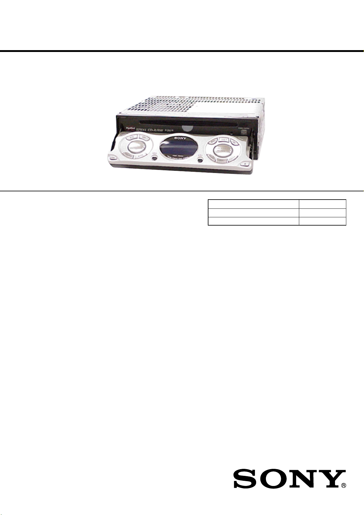
CDX-M630
SERVICE MANUAL
Ver 1.0 2002. 03
• The tuner and CD sections have no adjustments.
SPECIFICATIONS
AUDIO POWER SPECIFICATIONS (US MODEL)
POWER OUTPUT AND TOTAL HARMONIC DISTORTION
23.2 watts per channel minimum continuous average power into
4 ohms, 4 channels driven from 20 Hz to 20 kHz with no more
than 5% total harmonic distortion.
CD player section
Signal-to-noise ratio 90 dB
Frequency response 10 – 20,000 Hz
Wow and flutter Below measurable limit
Tuner section
FM
Tuning range 87.5 – 107.9 MHz (US, Canadian model)
87.5 – 108.0 MHz (AEP, UK, E model)
Antenna terminal External antenna connector
Intermediate frequency 10.7 MHz/450 kHz
Usable sensitivity 8 dBf
Selectivity 75 dB at 400 kHz
Signal-to-noise ratio 66 dB (stereo),
72 dB (mono)
Harmonic distortion at 1 kHz
0.6% (stereo),
0.3% (mono)
Separation 35 dB at 1 kHz
Frequency response 30 – 15,000 Hz
AM (US, Canadian model)
Tuning range 530 – 1,710 kHz
Antenna terminal External antenna connector
Intermediate frequency 10.7 MHz/450 kHz
Sensitivity 30 µV
US Model
Canadian Model
AEP Model
UK Model
E Model
Model Name Using Similar Mechanism CDX-L300/L460X
CD Drive Mechanism Type MG-393X-121//K
Optical Pick-up Name KSS-720A
MW/LW (AEP, UK, E model)
Tuning range MW: 531 – 1,602 kHz
LW: 153 – 279 kHz
Aerial terminal External aerial connector
Intermediate frequency 10.7 MHz/450 kHz
Sensitivity MW: 30 µV
LW: 40 µV
Power amplifier section
Outputs Speaker outputs (sure seal connectors)
Speaker impedance 4 – 8 ohms
Maximum power output 52 W × 4 (at 4 ohms)
General
Outputs Audio outputs (front/rear)
Subwoofer output (mono)
Power antenna relay
control terminal (US, Canadian model)
Power aerial relay
control terminal (AEP, UK, E model)
Power amplifier control
terminal
– Continued on next page –
FM/AM COMPACT DISC PLAYER
9-873-693-01
2002C0400-1
© 2002. 03
US, Canadian Model
FM/MW/LW COMPACT DISC PLAYER
AEP, UK, E Model
Sony Corporation
e Vehicle Company
Published by Sony Engineering Corporation
1
Page 2
k
CDX-M630
Inputs Telephone ATT control
terminal
Illumination control terminal (US, Canadian model)
BUS control input terminal
BUS audio input or AUX IN terminal
Remote controller input terminal
Antenna input terminal (US, Canadian model)
Aerial input terminal (AEP, UK, E model)
Tone controls US, Canadian model:
Bass ±10 dB at 62 Hz
Treble ±10 dB at 16 kHz
AEP, UK, E model:
Bass ±8 dB at 100 Hz
Treble ±8 dB at 10 kHz
Loudness +8 dB at 100 Hz
+2 dB at 10 kHz
Power requirements 12 V DC car battery
(negative ground)
Dimensions Approx. 178 × 50 × 182 mm
(7 1/8 × 2 × 7 1/4 in.)
(w/h/d)
Mounting dimensions Approx. 182 × 53 × 160 mm
(7 1/4 × 2 1/8 × 6 3/8 in.)
(w/h/d)
Mass Approx. 1.5 kg (2 lb. 10 oz.)
Supplied accessories Parts for installation and
connections (1 set)
Card remote commander
RM-X117
Note
This unit cannot be connected to a digital preamplifier or an equalizer.
Design and specifications are subject to change without
notice.
SERVICE NOTES
NOTES ON HANDLING THE OPTICAL PICK-UP BLOCK
OR BASE UNIT
The laser diode in the optical pick-up block may suffer electrostatic
breakdown because of the potential difference generated by the
charged electrostatic load, etc. on clothing and the human body.
During repair, pay attention to electrostatic breakdown and also use
the procedure in the printed matter which is included in the repair
parts.
The flexible board is easily damaged and should be handled with
care.
NOTES ON LASER DIODE EMISSION CHECK
The laser beam on this model is concentrated so as to be focused on
the disc reflective surface by the objective lens in the optical pickup block. Therefore, when checking the laser diode emission, observe from more than 30 cm away from the objective lens.
Notes on Chip Component Replacement
• Never reuse a disconnected chip component.
• Notice that the minus side of a tantalum capacitor may be dam-
aged by heat.
US model:
SAFETY-RELATED COMPONENT WARNING!!
COMPONENTS IDENTIFIED BY MARK 0 OR DOTTED LINE
WITH MARK 0 ON THE SCHEMATIC DIAGRAMS AND IN
THE PARTS LIST ARE CRITICAL TO SAFE OPERATION.
REPLACE THESE COMPONENTS WITH SONY P ARTS WHOSE
PART NUMBERS APPEAR AS SHOWN IN THIS MANUAL OR
IN SUPPLEMENTS PUBLISHED BY SONY.
ATTENTION AU COMPOSANT AYANT RAPPORT
À LA SÉCURITÉ!!
CAUTION
Use of controls or adjustments or performance of procedures
other than those specified herein may result in hazardous
radiation exposure.
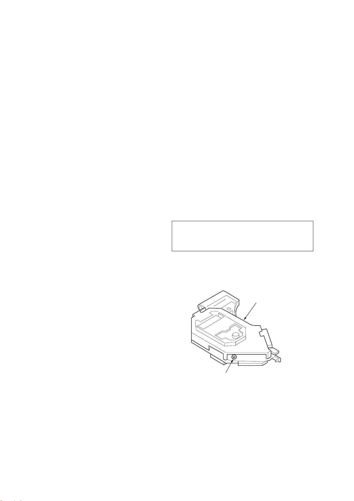
If the optical pick-up block is defective, please replace the whole
optical pick-up block.
Never turn the semi-fixed resistor located at the side of optical
pick-up block.
optical pick-up bloc
semi-fixed resistor
LES COMPOSANTS IDENTIFIÉS P AR UNE MARQUE 0 SUR LES
DIAGRAMMES SCHÉMATIQUES ET LA LISTE DES PIÈCES
SONT CRITIQUES POUR LA SÉCURITÉ DE FONCTIONNEMENT.
NE REMPLACER CES COMPOSANTS QUE PAR DES PIÈCES
SONY DONT LES NUMÉROS SONT DONNÉS DANS CE MANUEL
OU DANS LES SUPPLÉMENTS PUBLIÉS PAR SONY.
2
Page 3
CDX-M630
AEP, UK, E model:
This label is located on the bottom of the chassis.
This label is located on the drive unit’s internal chassis.
When replacing the chassis (T) of mechanism deck which have
the “CAUTION LABEL” attached, please be sure to put a new
CAUTION LABEL (3-223-913-11) to the chassis (T).
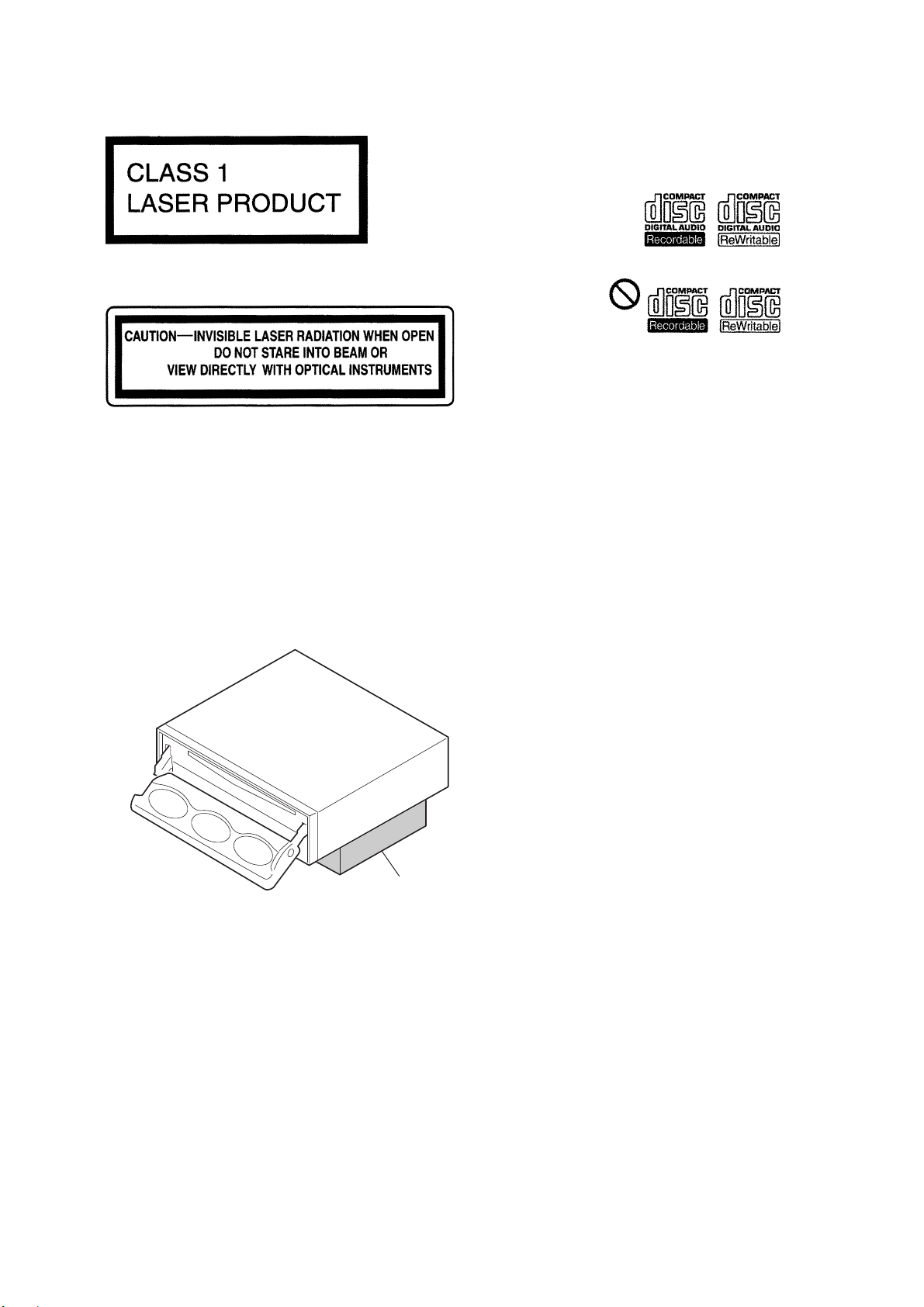
NOTE FOR THE OPENING OF THE FRONT PANEL
In this set, the front panel is lowered to below the bottom face when
it is opened.
When servicing the set, place it on a stand having a height of about
2 cm.
Notes on CD-R/CD-RW discs
• You can play CD-Rs (recordable CDs)/CD-RWs (rewritable CDs)
designed for audio use on this unit.
Look for these marks to distinguish CD-Rs/CD-RWs for audio
use.
These marks denote that a disc is not for audio use.
• Some CD-Rs/CD-RWs (depending on the equipment used for
its recording or the condition of the disc) may not play on this
unit.
• You cannot play a CD-R/a CD-RW that is not finalized∗.
∗ A process necessary for a recorded CD-R/CD-RW disc to be
played on the audio CD player.
stand
TEST DISCS
This set can playback CD-R and CD-ROM discs. The following
test discs should be used to check the capability:
CD-R test disc TCD-R082LMT (Part No. J-2501-063-1)
CD-RW test disc TCD-W082L (Part No. J-2501-063-2)
3
Page 4
CDX-M630
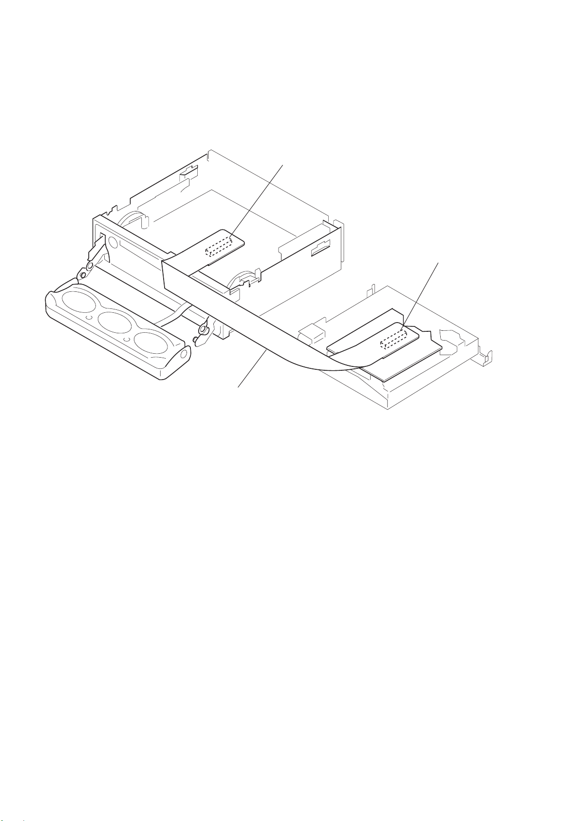
EXTENSION CABLE AND SERVICE POSITION
When repairing or servicing this set, connect the jig (extension cable)
as shown below.
• Connect the MAIN board (CNP701) and the SER VO board (CN1)
with the extension cable (Part No. J-2502-011-1).
MAIN BOARD CNP701
SERVO BOARD CN1
J-2502-011-1
4
Page 5

TABLE OF CONTENTS
CDX-M630
1. GENERAL
Location of Controls................................................................ 6
Connection example (US, Canadian Model)........................... 6
Connections (US, Canadian Model)........................................ 7
Connection example (AEP, UK Model) .................................. 8
Connections (AEP, UK Model) ............................................... 9
Connection example (E Model) ............................................ 10
Connections (E Model) ......................................................... 11
2. DISASSEMBLY
2-1. Front Panel Assy ............................................................... 12
2-2. CD Mechanism Block, Front Panel Assy..........................
2-3. Sub Panel (CD) Sub Assy ................................................. 13
2-4. Motor Block Assy, Cam (R) Assy ..................................... 14
2-5. Main Board ....................................................................... 14
2-6. Heat Sink ...........................................................................15
2-7. Chassis (T) Sub Assy ........................................................ 15
2-8. Lever Section, In Self SW Board ...................................... 16
2-9. Servo Board....................................................................... 16
2-10. Shaft Roller Assy, Load SW Board................................... 17
2-11. Floating Block Assy .......................................................... 17
2-12. Optical Pick-up Block ....................................................... 18
3. PHASE ALIGNMENT
3-1. Arm (A-L) Assy, Arm (B-L) Assy..................................... 19
3-2. Cam (L) ............................................................................. 19
3-3. Motor Block ...................................................................... 20
3-4. Alignment between Arm (A-L) Assy
and Arm (B-L) Assy .......................................................... 20
3-5. Arm (A-R) Assy, Arm (B-R) Assy .................................... 21
3-6. Cam (R) .............................................................................21
4. DIAGRAMS
4-1. IC Pin Descriptions ........................................................... 22
4-2. Block Diagram –CD Section–........................................... 27
4-3. Block Diagram –Tuner Section–....................................... 28
4-4. Block Diagram –Display Section–.................................... 29
4-5. Circuit Boards Location .................................................... 30
4-6. Schematic Diagram –CD Mechanism Section– ................31
4-7. Printed Wiring Boards –CD Mechanism Section–............ 32
4-8. Printed Wiring Boards –Main Section– ............................ 34
4-9. Schematic Diagram –Main Section (1/4)– ........................36
4-10. Schematic Diagram –Main Section (2/4)– ........................37
4-11. Schematic Diagram –Main Section (3/4)– ........................38
4-12. Schematic Diagram –Main Section (4/4)– ........................39
4-13. Printed Wiring Board –Sub (CD) Section–....................... 40
4-14. Schematic Diagram –Sub (CD) Section–.......................... 41
4-15. Printed Wiring Board –Display Section–.......................... 42
4- 16. Schematic Diagram –Display Section–............................. 43
5. EXPLODED VIEWS
5-1. Chassis Section ................................................................. 46
5-2. Cam Section ...................................................................... 47
5-3. Main Board Section .......................................................... 48
5-4. Front Panel Section ........................................................... 49
5-5. CD Mechanism Section (1) ...............................................50
5-6. CD Mechanism Section (2) ...............................................51
5-7. CD Mechanism Section (3) ...............................................52
6. ELECTRICAL PARTS LIST ........................................ 53
5
Page 6
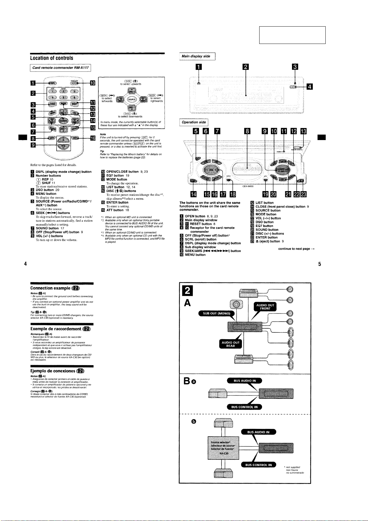
CDX-M630
(US, Canadian Model)
SECTION 1
GENERAL
This section is extracted
from instruction manual.
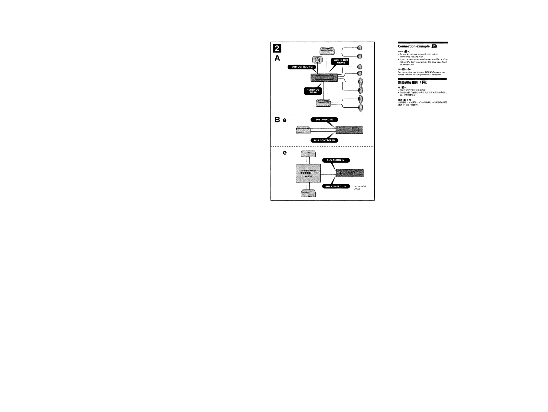
Connection example (US, Canadian Model)
6
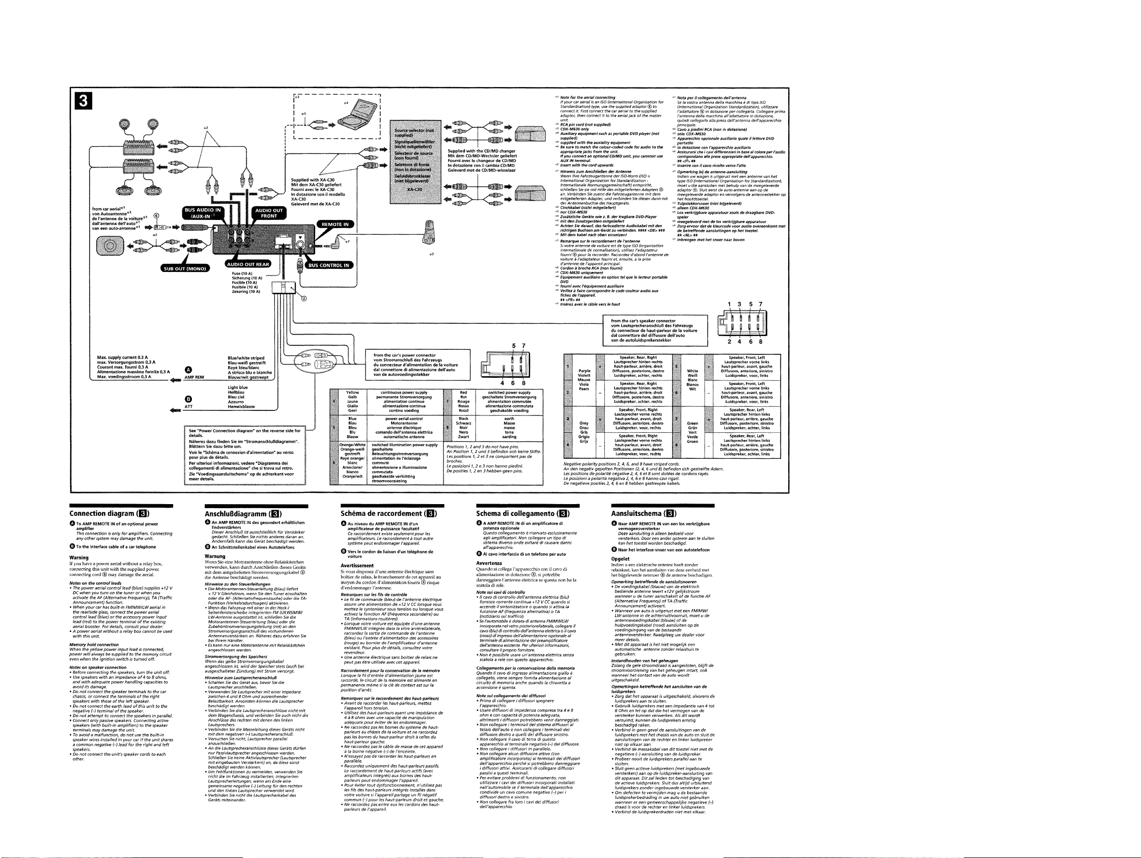
Page 7
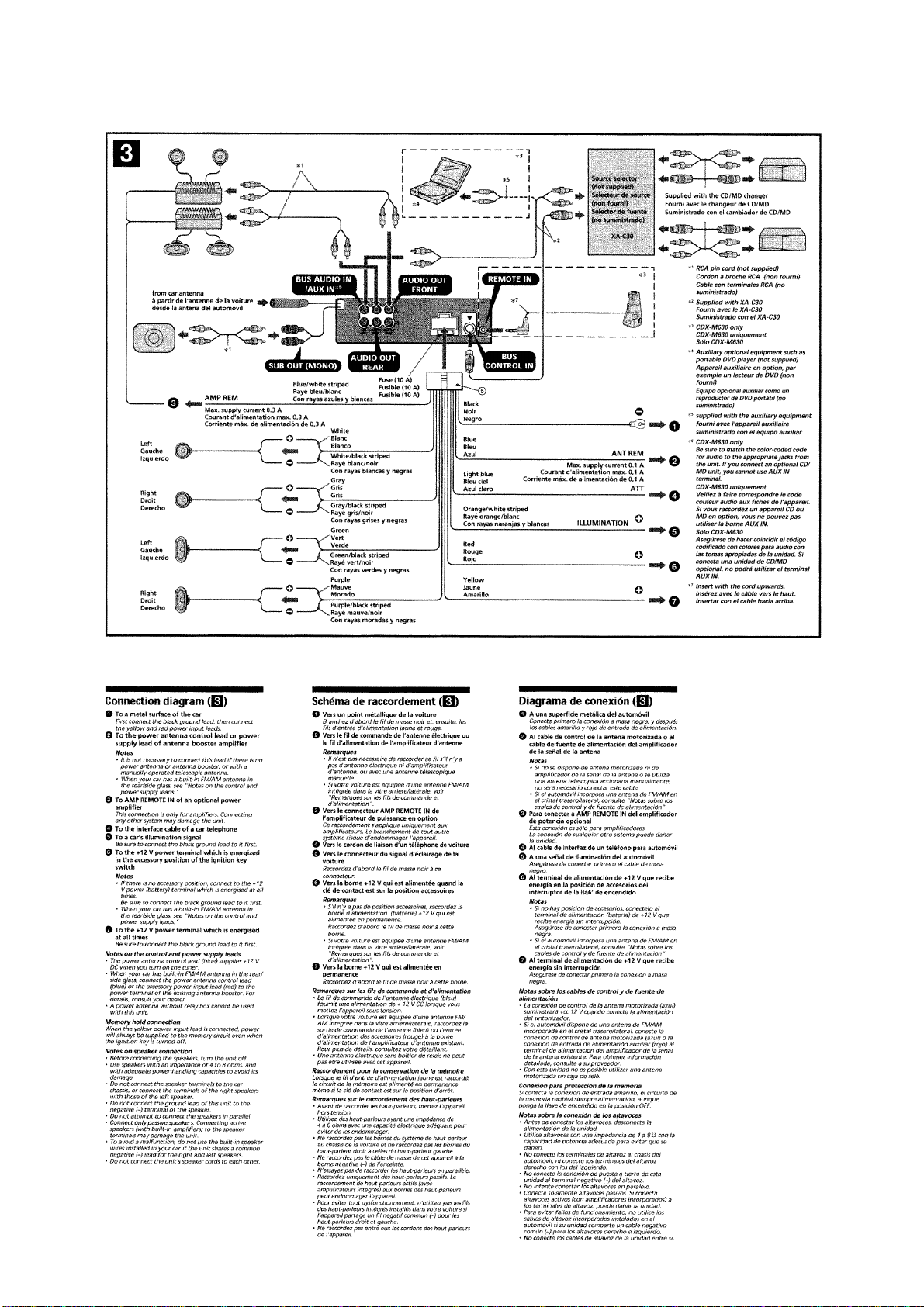
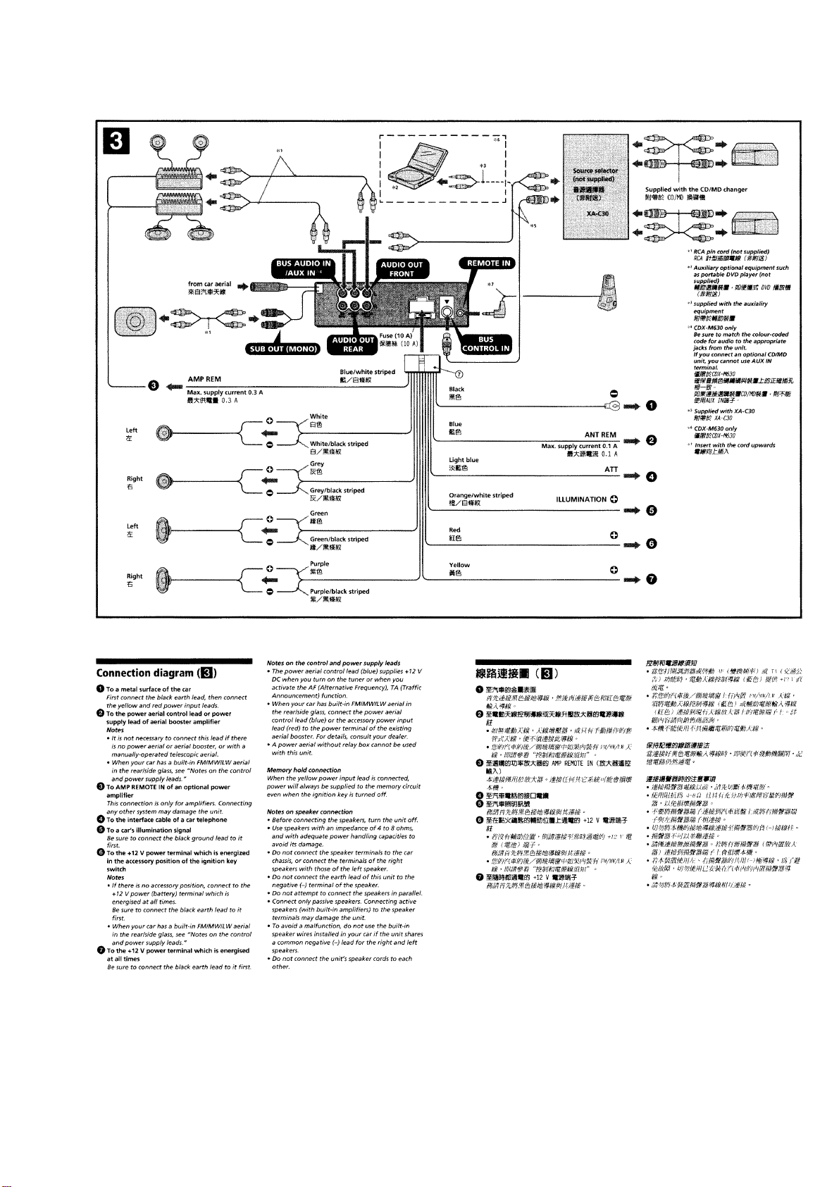
Connections (US, Canadian Model)
CDX-M630
7
Page 8
CDX-M630
Connection example (AEP, UK Model)
8
Page 9
Connections (AEP, UK Model)
CDX-M630
99
Page 10
CDX-M630
Connection example (E Model)
1010
Page 11
Connections (E Model)
CDX-M630
11
Page 12
CDX-M630
SECTION 2
DISASSEMBLY
Note : This set can be disassemble according to the following sequence.
SET
2-7. CHASSIS (T) SUB ASSY
2-1. FRONT PANEL ASSY
(Page 12)
(Page 15)
2-2. CD MECHANISM BLOCK,
FRONT PANEL ASSY
(Page 13)
2-8. LEVER SECTION,
IN SELF SW BOARD
(Page 16)
2-3. SUB PANEL (CD) SUB ASSY
(Page 13)
2-4. MOTOR BLOCK ASSY,
CAM (R) ASSY
(Page 14)
2-5. MAIN BOARD
(Page 14)
2-6. HEAT SINK
(Page 15)
Note : Follow the disassembly procedure in the numerical order given.
2-10. SHAFT ROLLER ASSY,
LOAD-SW BOARD
(Page 17)
2-11. FLOATING BLOCK ASSY
(Page 17)
2-12. OPTICAL PICK-UP BLOCK
(Page 18)
2-9. SERVO BOARD
(Page 16)
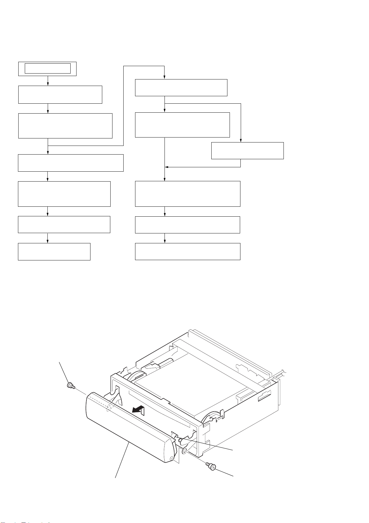
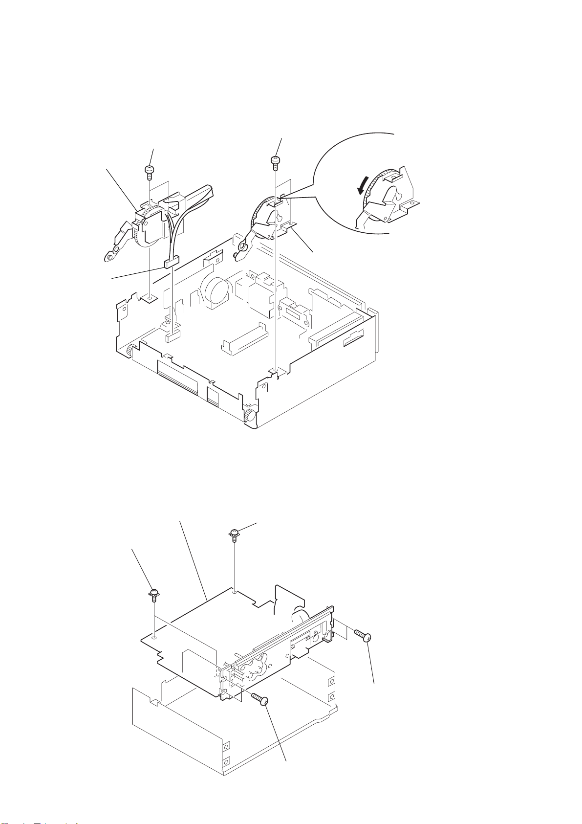
2-1. FRONT PANEL ASSY
2
screw (panel)
3
front panel assy
4
(Take care not to pull the
flexible board excessively)
flexible board
1
screw (panel)
12
Page 13
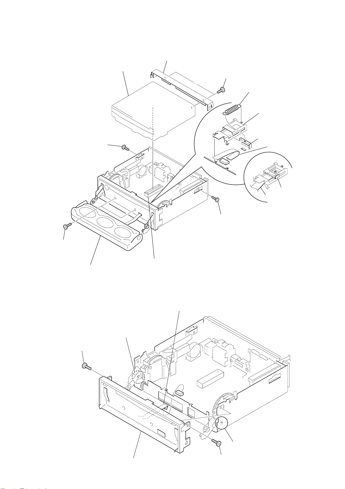
2-2. CD MECHANISM BLOCK, FRONT PANEL ASSY
7
bracket (CD)
5
CD mechanism block
3
PTT 2.6x4
6
PTT 2.6x6
8
tension spring (flexible)
0
cover (flexible)
9
slider (flexible)
qa
CNP802
CDX-M630
1
PTT 2.6x6
qs
front panel assy
2-3. SUB PANEL (CD) SUB ASSY
4
3
PTT 2.6x6
claw
4
CNP701
1
CNP805
2
PTT 2.6x4
slider (flexible)
flexible board
Note: When installing
the flexible board,
make the board slack
as illustrated.
6
sub panel (CD) sub assy
5
2
PTT 2.6 x6
claw
13
Page 14
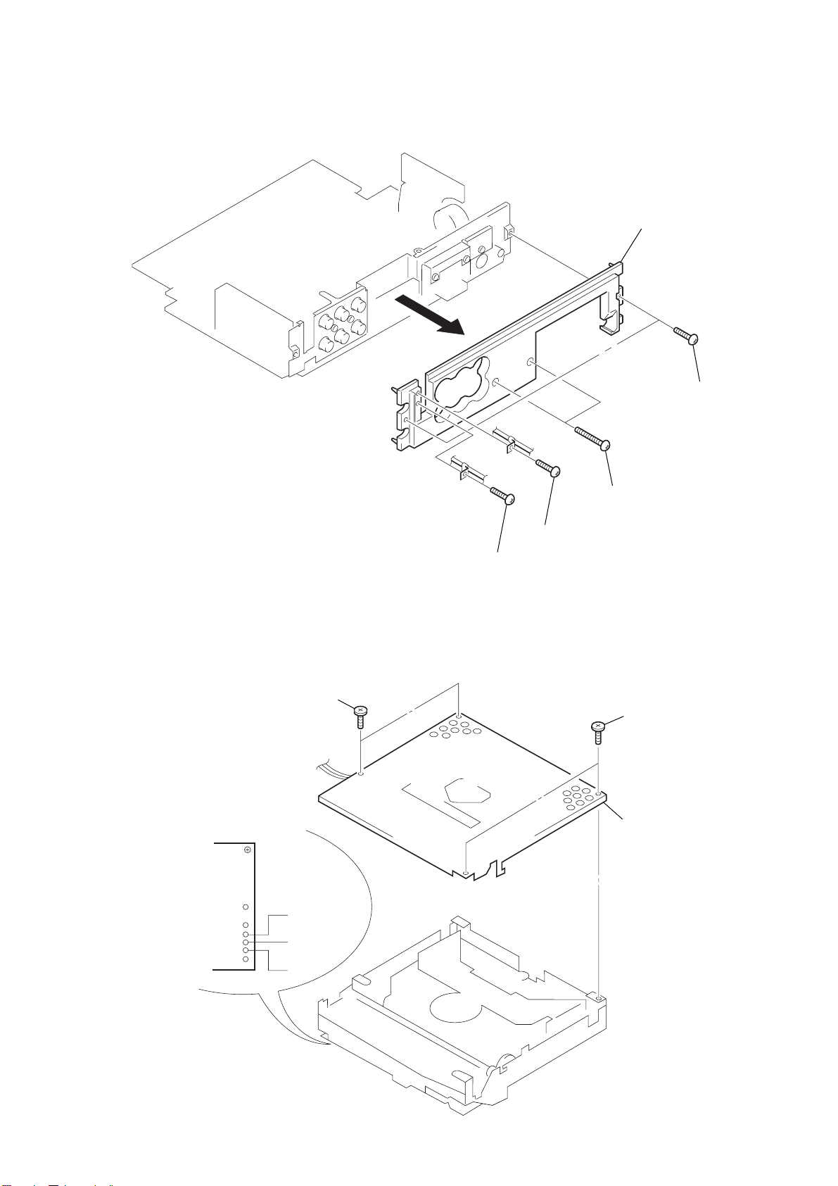
CDX-M630
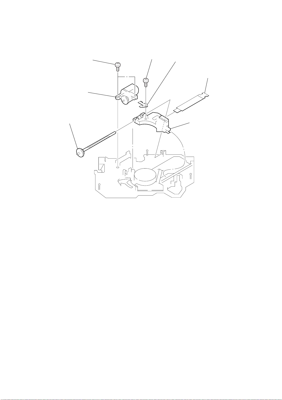
h
6
2-4. MOTOR BLOCK ASSY, CAM (R) ASSY
Note : Install the motor block assy and cam (R) assy in this roder.
For phase alignment between cams (L) and (R), see page 19 and 21.
4
PTT 2.6x6
5
motor block assy
3
CNP902
1
PTT 2.6x6
2
cam (R) assy
Note: Install the cam (R) assy wit
the cam fully rotated in the
direction of the arrow
A
A
.
2-5. MAIN BOARD
5
3
PTT 2.6x6
ground point
MAIN board
4
PTT 2.6x6
ground point
2
PTT 2.6x
14
1
PTT 2.6x6
Page 15
6
2-6. HEAT SINK
5
heat sink
CDX-M630
4
PTT 2.6x
2-7. CHASSIS (T) SUB ASSY
1
Unsolder the
lead wires.
2
P 2x3
2
PTT 2.6x6
1
PTT 2.6x6
3
PTT 2.6x10
3
P 2x3
4
chassis (T) sub assy
black
red
white
15
Page 16
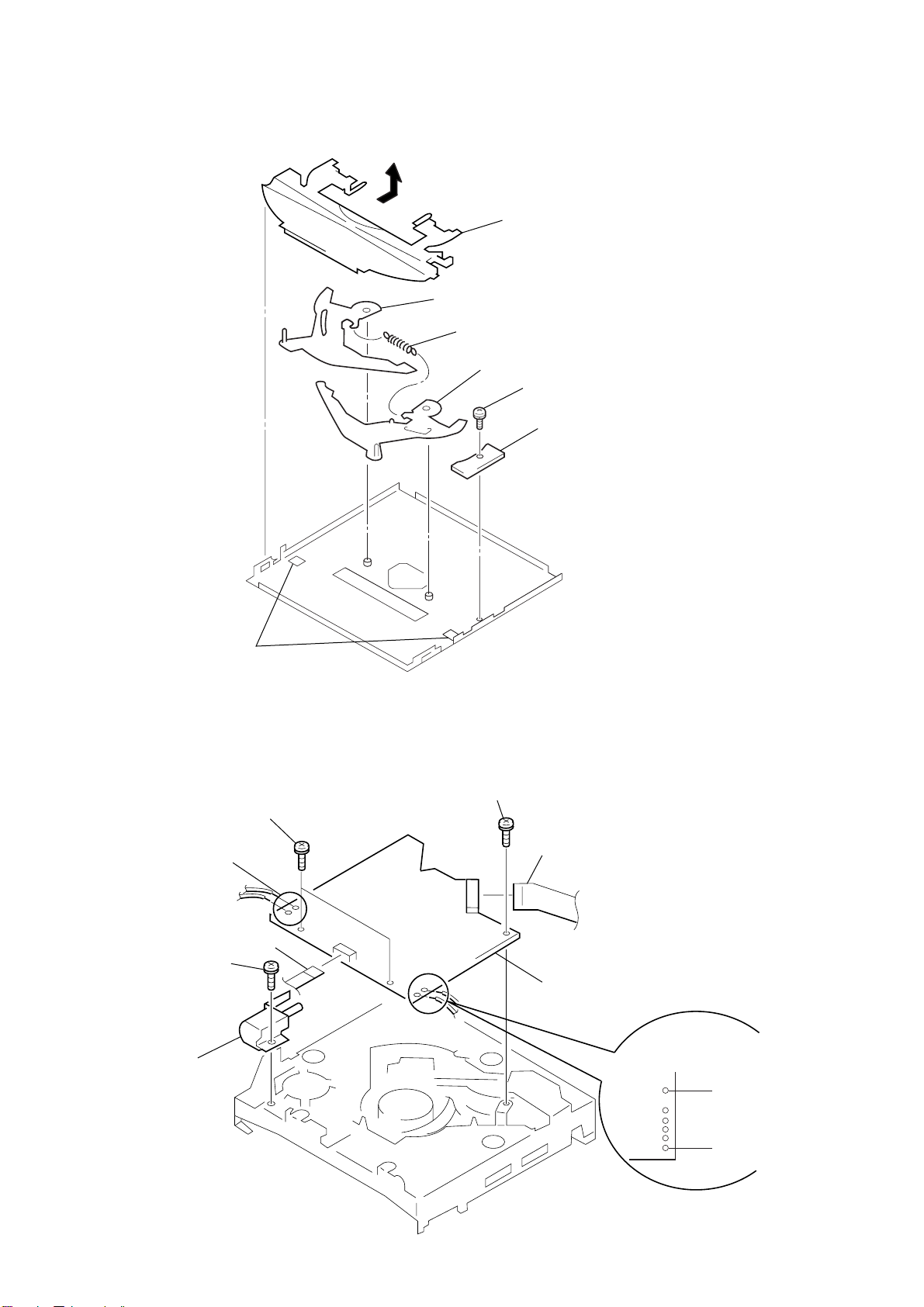
CDX-M630
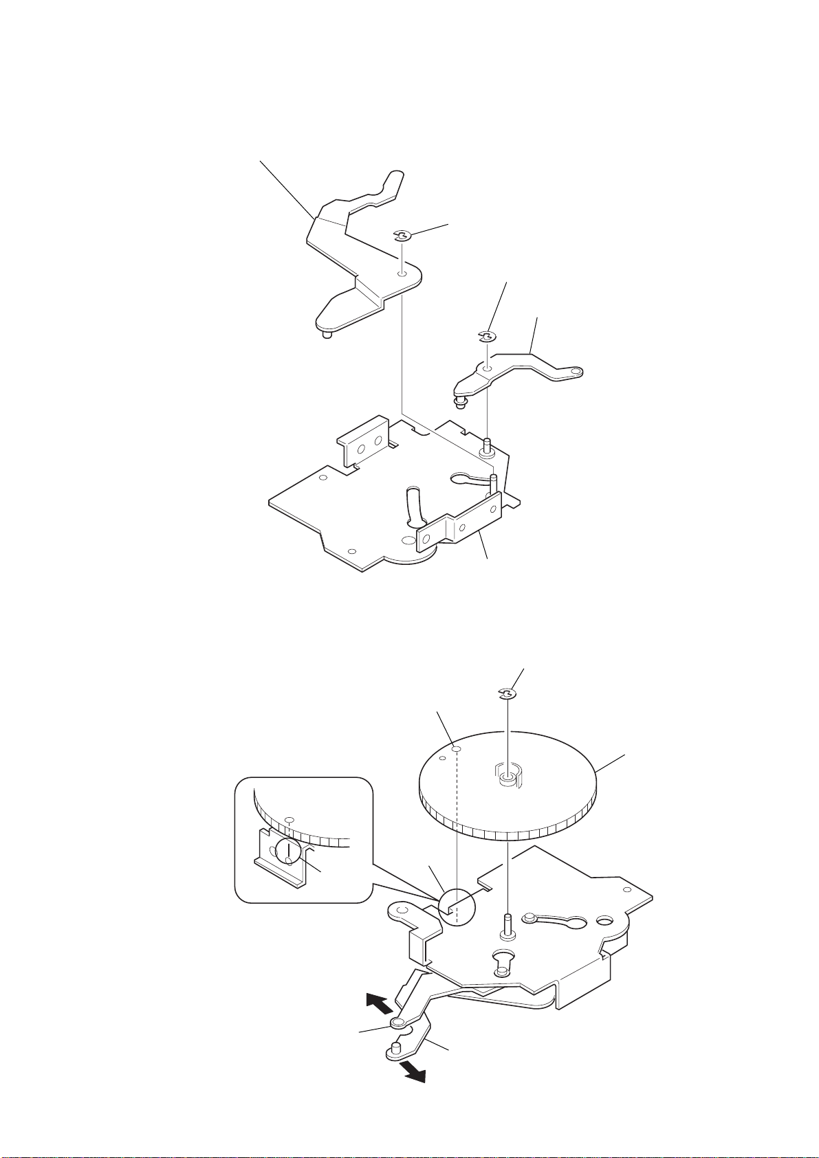
2-8. LEVER SECTION, IN SELF SW BOARD
6
lever (R)
3
tension spring (LR)
7
lever (L)
5
guide (disc)
1
special screw
2
IN SELF SW board
2-9. SERVO BOARD
3
Removal the solders.
6
loading motor assy
(M903)
4
claws
8
special screws
5
P 2x3
1
CN3
7
special screw
2
9
CN2
SERVO board
4
Unsolder the
lead wires.
blu
16
yel
Page 17
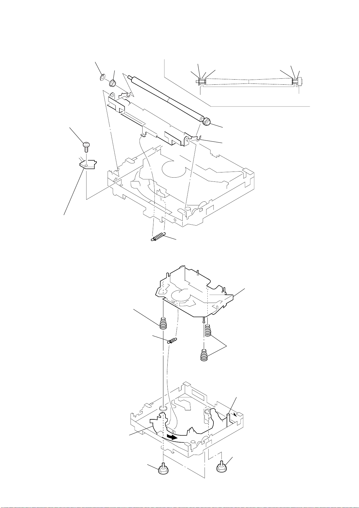
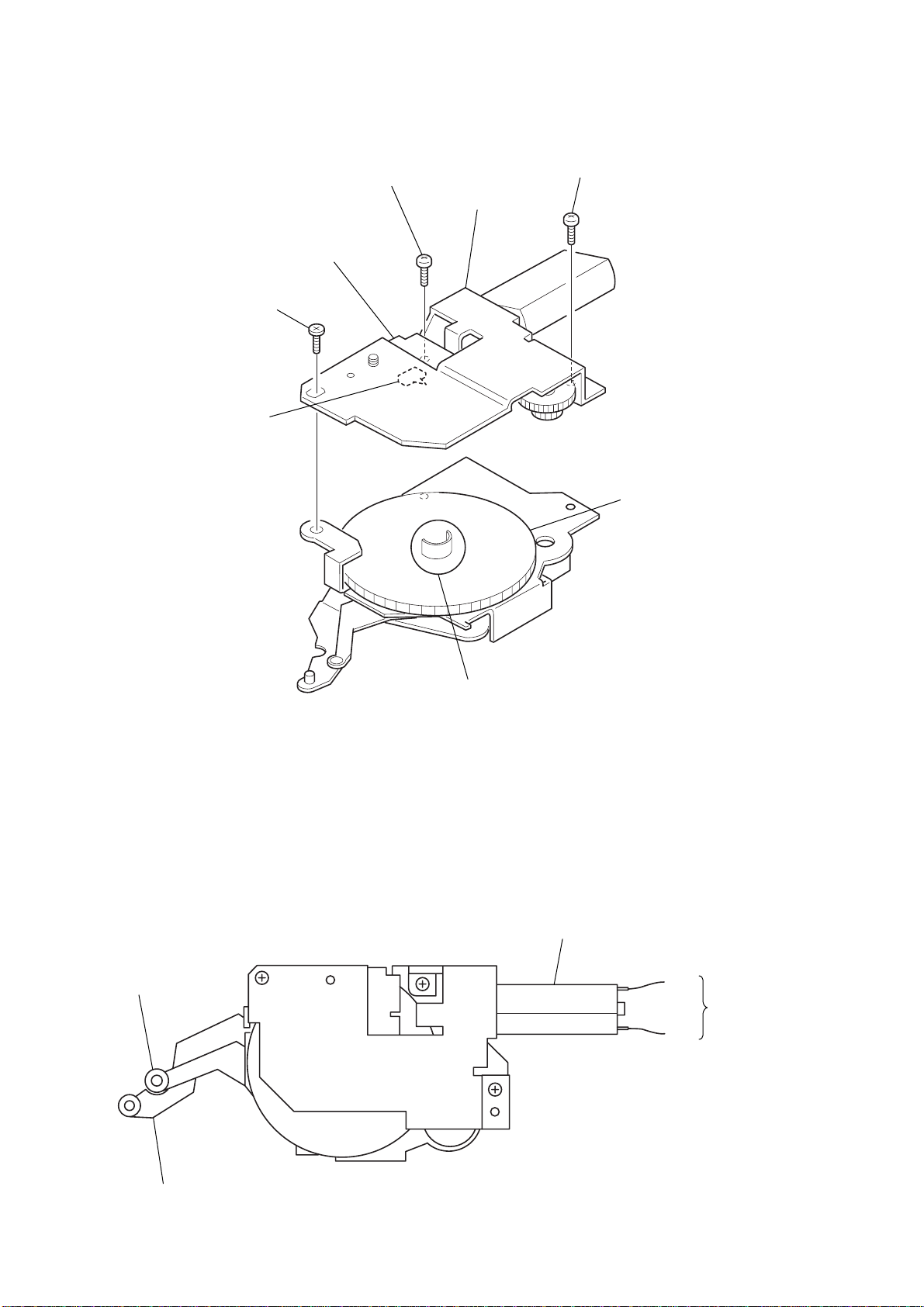
2-10. SHAFT ROLLER ASSY, LOAD-SW BOARD
3
retaing ring (RA)
4
6
special screw
shaft retainer (roller)
retaing ring
(RA)
shaft retainer (roller)
arm
washer
5
2
Fig. 1
shaft roller assy
arm (roller)
washer
CDX-M630
arm
shaft retainer
(roller)
7
LOAD-SW board
2-11. FLOATING BLOCK ASSY
7
compression spring (FL)
1
tension spring (KF1)
1
tension spring (RA)
6
floating block assy
8
compression spring (FL)
5
Turn loading ring in the
direction of the arrow.
3
damper (T)
4
Fit lever (D) in the
direction of the arrow.
2
damper (T)
17
Page 18
CDX-M630
2-12. OPTICAL PICK-UP BLOCK
1
P 2x3
2
sled motor assy
7
shaft (feed) assy
5
P 2x3
6
spring (feed), plate
3
optical pick-up block
4
pick-up flexible board
18
Page 19
)
3-1. ARM (A-L) ASSY, ARM (B-L) ASSY
y
3
arm (A-L) assy
SECTION 3
PHASE ALIGNMENT
4
stop ring 1.5, type-E
2
stop ring 1.5, type-E
1
arm (B-L) ass
CDX-M630
3-2. CAM (L)
1 Move the arm (B-L) assy in the direction of the
arrow A and the arm (A-L) assy in the direction of
the arrow B fully (full open state).
2 Align the hole (large) on the cam (L) with part C and
install the cam.
4 Turn the cam (L) clockwise and counterclockwise to
verify that both the arms are operated.
line
bracket (L) assy
stop ring 1.5, type-E
3
hole(large)
cam (L
C
arm (B-L) assy
A
arm (A-L) assy
B
19
Page 20
CDX-M630
)
V
3-3. MOTOR BLOCK
1 Turn the cam (L) and position the cam so that part A
does not touch the SW board SW900.
SW board
5
PTT 2.6x6
SW900
4
PTT 2.6x6
2
motor block
3
PTT 2.6x6
3-4. ALIGNMENT BETWEEN ARM (A-L) ASSY
AND ARM (B-L) ASSY
1 Input 9V DC to the motor terminal until the cam (L)
stops rotating.
Take care to avoid overload of the motor.
2 Verify that the arm (A-L) assy and arm (B-L) assy
are positioned as shown below (full open).
cam (L
A
motor
20
arm (B-L) assy
arm (A-L) assy
+B
DC 9
GND
Page 21

3-5. ARM (A-R) ASSY, ARM (B-R) ASSY
y
2
stop ring 1.5, type-E
1
arm (B-R) assy
3
arm (A-R) assy
4
stop ring 1.5, type-E
CDX-M630
3-6. CAM (R)
1 Move the arm (B-R) assy in the direction of the
arrow A and the arm (A-R) assy in the direction of
the arrow B fully (full open state).
2 Align the hole (large) on the cam (R) with part C and
install the cam.
4 Turn the cam (R) clockwise and counterclockwise to
verify that both the arms are operated.
line
C
hole(large)
bracket (R) ass
3
stop ring 1.5, type-E
A
cam (R)
arm (B-R) assy
5
damper, oil
6
screw (P 2x4)
B
arm (A-R) assy
21
Page 22

CDX-M630
SECTION 4
DIAGRAMS
4-1. IC PIN DESCRIPTIONS
• IC801 MB90574CPMT-G-371-BNDE1 (SYSTEM CONTROL) (US, Canadian Model)
• IC801 MB90574CPMT-G-372-BNDE1 (SYSTEM CONTROL) (AEP, UK, E Model)
Pin No. Pin Name I/O Pin Description
1 CD RESET O Servo CPU reset signal output to servo IC (IC1)
2 NCO O Not used. (Open)
3A0OServo CPU command/parameter discriminate signal output to servo IC (IC1)
4 NCO O Not used. (Open)
5ATT O System mute control signal output
6 SYSRST O System reset signal output to bus interface (IC802)
7 STB O Servo CPU data strobe signal output to servo IC (IC1)
8 VCC — Power supply pin (+5 V)
9XTAL EN O Servo CPU crystal oscillator control signal output to servo IC (IC1)
10 E2PSIO I/O EEPROM data signal input/output with tuner unit (TU601)
11 E2PCKO O EEPROM clock signal output to tuner unit (TU601)
12 FLS SI I Flash write-in data signal input
13 FLS SO O Flash write-in data signal output
14 BUS ON O BUS ON control signal output to sub system control (IC301)
15 BEEP O Beep signal output
16 TEL ATT I Telephone mute detect signal input
17 UNI SI I SONY BUS data signal input from bus interface (IC802)
18 UNI SO O SONY BUS data signal output to bus interface (IC802)
19 UNI CKO O
20 LIMIT I CD limit SW signal input (SW4)
21 PH1 I CD PH1 detect signal input Not used in this set. (Open)
22 DSW I CD disc SW detect signal input (SW5)
23 IN/PH2 I CD IN SW/PH2 detect signal input (SW6)
24 SIRCS I Remote control data signal input from sircs interface (IC803)
25 CD TSI I Servo CPU serial data signal input from servo IC (IC1)
26 CD TSO O Servo CPU serial data signal output to servo IC (IC1)
27 CD TCK O Servo CPU serial clock signal output to servo IC (IC1)
28 RF OK I Servo CPU RFOK signal input from servo IC (IC1)
29 TSTB O Servo CPU CD TEXT strobe signal output to servo IC (IC1)
30 NCO O Not used. (Open)
31 VOL ATT O Electronic volume mute signal output to electronic volume (IC305)
32 NCO O Not used. (Open)
33 VSS — Ground pin
34 C — Condenser pin for voltage stabilizer
35 SELF SW I CD self SW signal input (SW2)
36 PH3 I CD PH3 detect signal input Not used in this set. (Open)
37 SHIFT O OSC frequency shift signal output for DC-DC converter (IC901)
38 DVCC — Power supply pin (+5 V)
39 DVSS — Ground pin
40 FP CTRL O Front panel open/close speed control signal output
41 NCO O Not used. (Open)
42 AVCC — Power supply pin (+5 V)
43 AVRH — Power supply pin (+5 V)
44 AVRL — Ground pin
45 AVSS — Ground pin
46 KEY IN0 I Key signal input 0
47 KEY IN1 I Key signal input 1
48 RC IN0 I Rotary commander signal input 0
49 NCO O Not used. (Open)
SONY BUS clock signal output to bus interface (IC802)
and sub system control (IC301)
22
Page 23

CDX-M630
Pin No. Pin Name I/O Pin Description
50 QUALITY I Tuner noise detect signal input from electronic volume (IC305) (AEP, UK, E Model)
51 FM AGC O FM auto gain control signal output to tuner unit (TU601)
52 MPTH I Tuner multi-path signal input from RDS decoder (IC601) (AEP, UK, E model)
53 VSM I S-meter signal input from tuner unit (TU601)
54 VCC — Power supply pin (+5 V)
55 AMP ON O AMP ON control signal output to power amp (IC903)
56 NS MASK O Tuner nose masking signal output (AEP, UK, E model)
57 DDC ON O DC-DC converter control signal output
58 LOAD O CD loading motor control signal output to loading motor drive (IC2)
59 EJECT O CD eject motor control signal output to eject motor drive (IC2)
60 BUS/AUX O BUS/AUX audio ground select signal
61 OPEN KEY I OPEN key signal input (LSW60)
62 NOSE SW I Front panel attach/detach detect signal input
63 VSS — Ground pin
64 DETACH SW I Front panel detach detect signal input
65 PWM I DC-DC converter OSC frequency count signal
66 to 68 NCO O Not used. (Open)
69 FLASH W I Flash write-in mode detect signal input
70 I2C SIO O I2C serial data signal output
71 I2C CKO O I2C serial clock signal output
72 KEY ACK I Key acknowledge detect signal input
73 X1A — Crystal oscillator (32.768 kHz)
74 X0A — Crystal oscillator (32.768 kHz)
75 DAVN I
76 CD ON O CD mechanism power control signal output
77 BU IN I Back-up power supply detect signal input from bus interface (IC802)
78 CD PACK I Servo CPU CD TEXT PACK synchro signal input from servo IC (IC1)
79 RC IN1 I Rotary commander signal input 1 from remote in jack (CNP803)
80 AD ON O A/D converter power control signal output
81 ACC IN I Accessory key ON signal input
82 FLSW PW ON O Flash write-in jig power control signal output
83 PW ON O System power control signal output
84 TEST IN I Test mode setting detect signal input
85 RAM BU I RAM reset detect signal input
86 HSTX I Hardware standby setting input
87 MD2 I Operation mode setting 2 input Connect to ground in this set.
88 MD1 I Operation mode setting 1 input Connect to VDD in this set.
89 MD0 I Operation mode setting 0 input Connect to VDD in this set.
90 RSTX I CPU reset input
91 VSS — Ground pin
92 X0 — Crystal oscillator (3.68 MHz)
93 X1 — Crystal oscillator (3.68 MHz)
94 VCC — Power supply pin (+5 V)
95 ILL IN I Illumination line detect signal input
96 I DET I Front panel current detect signal input
97 MOT – O Front panel open/close motor control signal output to motor drive (IC307)
98 MOT + O Front panel open/close motor control signal output to motor drive (IC307)
99 CLOSW SW I Front panel close detect signal input (SW900)
100 OPEN SW I Front panel open detect signal input (SW900)
101 CENTER SW I Front panel center position detect signal input
102 MODEL SEL I Fix/Detach model select setting signal input
103 NCO O Not used. (Open)
RDS data block synchro detect signal input from RDS decoder (IC601)
(AEP, UK, E model)
23
Page 24

CDX-M630
Pin No. Pin Name I/O Pin Description
104 DST SEL1 I Destination select 1 signal input
105 DST SEL2 I Destination select 2 signal input
106 BOOT O Display CPU write-in control signal output to sub system control (IC301)
107 S CODE1 I Security code setting 1 signal input
108 S CODE2 I Security code setting 2 signal input
109 S CODE3 I Security code setting 3 signal input
110S CODE4 I Security code setting 4 signal input
111 CDM ON O CD mechanism power voltage control signal output
112 NCO O Not used. (Open)
113 NCO O Not used. (Connect to ground.)
114 TUN ON O Tuner ON control signal output
115 LED SW1 O Front panel illumination control signal output to sub system control (IC301)
116 LED SW2 O Control panel illumination control signal output to sub system control (IC301)
117 ADSO1 O ADSO signal output 1 to ADSO SWITCH (IC407)
118 ADSO2 O ADSO signal output 2 to ADSO SWITCH (IC407)
119 VSS — Ground pin
120 NCO O Not used. (Open)
24
Page 25

• IC301 HD6432398A03FW (SUB SYSTEM CONTROL)
Pin No. Pin Name I/O Pin Description
1 SA CLK O Spectrum analyzer clock signal output to electronic volume (IC305)
2 NCO O Not used. (Open)
3 VSS — Ground pin
4NC—Not used. (Open)
5 VCC — Power supply pin (+5 V)
6 to 9 NCO O Not used. (Open)
10 VSS — Ground pin
11 to 18 NCO O Not used. (Open)
19 VSS — Ground pin
20 to 27 NCO O Not used. (Open)
28 VSS — Ground pin
29 to 31 NCO O Not used. (Open)
32 SA EN I Spectrum analyzer enable signal input from system control (IC801)
33 NCO O Not used. (Open)
34 BU IN I Back-up voltage detect signal input from bus interface (IC802)
35, 36 VSS — Ground pin
37 NCO O Not used. (Open)
38 BUS ON I BUS ON signal input from system control (IC801)
39 VCC — Power supply pin (+5 V)
40 to 43 NCO O Not used. (Open)
44 VSS — Ground pin
45 NCO O Not used.
46 LED SW1 I Illumination select control 1 signal input from system control (IC801)
47 LED SW2 I Illumination select control 2 signal input from system control (IC801)
48, 49 NCO O Not used. (Open)
50 LINK OFF O LINK OFF signal output
51 NCO O Not used. (Open)
52 ILL ON O Illumination control signal output
53 VSS — Ground pin
54 to 56 NCO O Not used. (Open)
57 BOOT I Display CPU write-in control signal input from system control (IC801)
58 VCC — Power supply pin (+5 V)
59 NCO O Not used. (Open)
60 TX/LCD SO O LCD data output/UART signal output
61 NCO O Not used.
62 RX I UART signal input
63 NCO O Not used.
64 LCD CKO O LCD clock signal output to LCD driver (IC1 and 2)
65 VSS — Ground pin
66 LCD CE0 O LCD driver chip enable 1 signal output to LCD driver (IC2)
67, 68 VSS — Ground pin
69 LCD INH O LCD driver inhibit signal output to LCD driver (IC1 and 2)
70 LCD CE1 O LCD driver chip enable 2 output to LCD driver (IC1)
71 LCD CE2 O LCD driver chip enable 3 output to LCD driver
72 to 78 NCO O Not used. (Open)
79 FL W O Not used. (Open)
80 VCL I Connecting to ground through a capacitor. Not used in this set. (Open)
81 RES I Reset signal input
82 NMI (H) I Non maskable interrupt signal input
83 ST/SY (H) I Stanby mode signal input
84 VCC — Power supply pin (+5 V)
85 XTAL — Crystal oscillator (18.43 MHz)
CDX-M630
25
Page 26

CDX-M630
Pin No. Pin Name I/O Pin Description
86 EXTAL — Crystal oscillator (18.43 MHz)
87 VSS — Ground pin
88 PF7 O Not used. (Open)
89 VCC — Power supply pin (+5 V)
90 to 96 NCO O Not used. (Open)
97 UNI SO O Bus data signal output to bus interface (IC802)
98 UNI SI I Bus data signal input from bus interface (IC802)
99 VSS — Ground pin
100 VSS — Ground pin
101 UNI SCK I Bus clock signal input from system control (IC801)
102 P53 O Not used. (Open)
103 AVCC — Power supply pin (+5 V)
104 VREF — Reference voltage (+5 V)
105 to 111 NIL I Connect to ground in this set.
112 SA IN I SA data signal input from electronic volume (IC305)
113AVSS — Ground pin
114 VSS — Ground pin
115 to 122 NCO O Not used. (Open)
123 MD0 (H) — Mode pin
124 MD1 (H) — Mode pin
125 MD2 (H) — Mode pin
126 to 128 NCO O Not used. (Open)
26
Page 27

4-2. BLOCK DIAGRAM — CD SECTION —
OPTICAL PICK-UP
KSS-720A
RF AMP,DIGITAL SERVO
DIGITAL SIGNAL PROCESSOR
IC1
CDX-M630
PD
LD
A
C
B
D
E
F
FOCUS
COIL
I-V
CONV.
LD
DRIVE
Q1
A
82
C
83
B
84
D
85
E
87
F
86
PD
97
A+5V
LD
98
FOCUS/TRACKING COIL DRIVE,
SLED/SPINDLE/LOADING MOTOR DRIVE
FCS-
15
FCS+
16
TRACKING
APC
IC2
FOCUS
COIL
DRIVE
ERROR
(Page 28)
TUNER
LOUT
RF
EQ
FORCUS
ERROR
FD
26
EFM
DEMOD
SERVO
CTL
FDTDSD
62 63 64 65
MD
D/A
CONV
DSUB CODE
PROCESS
I/F
OSC
23 24
X1
16.9344MHz
ROUT
PACK
TSTB
TSCK
TSI
SCK
STB
RST
RFOK
XTALEN
16
12
R-CH
52
56
55
54
SI
8
SO
7
6
5
AO
4
3
2
9
SW5
(DOWN)
CDL
SECTION
A
SYSTEM CONTROL
78
CD_PACK
29
TSTB
26
CD_TSO
25
CD TSI
27
CD TCK
7
STB
3
AO
1
CD_RST
28
RFOK
9
XTALEN
22
D SW
IC801 (1/3)
TRACKING
COIL
• Signal path
:CD
• R-ch is omitted due to
same as L-ch.
M902
(SLED)
M901
(SPINDLE)
M903
(LOADING)
35
23
20
58
59
76
SELFSW
IN/PH2
LIMIT
LOAD
EJECT
CD ON
(DISC IN)
BATT
CD+6V
SW2
(SELF)
SW3
SW4
(LIMIT)
TRK+
17
TRK-
18
SL-
M
13
SL+
14
SP-
M
11
SP+
12
LD-
M
9
LD+
10
TRACKING
COIL
DRIVE
SLED
MOTOR
DRIVE
SPINDLE
MOTOR
DRIVE
LOADING
MOTOR
DRIVE
TD
23
SD
5
MD
6
LOAD
1
EJECT
2
A+5V
AU+5V
D+5V
DR+6V
CD POWER
CONTROL
Q913-915
CD POWER
CONTROL
Q929,930
27 27
Page 28

CDX-M630
4-3. BLOCK DIAGRAM — TUNER SECTION —
(Page 27)
CD
A
SACLK
B
SAOUT
10
8
FM AMP
Q607
9
X601
4.3MHz
14
12
13
17
18
4
• Signal path
: FM
: AM/MW
: CD
• R-ch is omitted due to
same as L-ch.
AJ1
(ANTENNA)
1
2
ANT AM
ANT FM
SECTION
DISPLAY
SECTION
(Page 29)
TUNER UNIT
TU601
MPX
AMDET
RDS
S METER VSM
SDA
SCL
SDA
EEPROM
SCL
FM AGC
CDL
IC311 (1/2)
AEP,UK,E MODEL
NOISE
CANCEL
IC602
RDS DECODER
IC601
16
FM DET
4
XO
5
XI
20
S METER
ADSO SWITCH
15
SDA
SCL
MPTH
DAVN
IC407
Q605
PJ401
–1
PJ402
CNP901
–2
–5
–6
–3
–4
–1
–2
1
9
2
10
4
12
3
11
13
14
7
15
5
6
19
17
18
16
FL+
FL–
RL+
RL–
FR+
FR–
RR+
RR–
TEL MUTE
ILL
ACC
TEST
AMP REM
ANT REM
B+
B+
L
BUS AUDIO IN
R
L
AUDIO OUT
FRONT
R
L
AUDIO OUT
REAR
R
L
SUB OUT (MONO)
R
F901
D912
D905,914
GND SWITCH
Q420
Q202
Q201
Q403
BATT
FL
RL
POWER AMP
12
11
22
MUTE
4
STBY
Q917
Q901
IC905
+5V
REG
IC903
POWER
CONT
Q461
12
R-CH
R-CH
R-CH
5
3
9
7
R-CH
BATT
BATT
ELECTRONIC VOLUME
IC305
4
AUXL
43
MDL
21
SACLK
23
SA OUT
38
1
AC OUTL
33
AC INL
12
MPX1
9
AM
14
MP IN
13
LEVEL
19
SDA
20
SCL
16
QUAL
17
SM
SYSTEM CONTROL
IC801 (2/3)
31
VOL ATT
50
QUALITY
56
NS MASK
52
MPTH
75
DAVN
53
I2CSIO
70
I2CCKO
71
E2PSIO
10
E2PCKO
11
FM AGC
51
IC311 (2/2)
3
2
9
10
2
8
OUT LF
OUT LR
OUT LR
ADSO1
ADSO2
BUS/AUX
ATT
AMP ON
TEL ATT
ILL IN
ACC IN
X1A
X0A
TEST IN
PW ON
TUN ON
28
27
23
117
118
60
55
16
95
81
73
74
84
83
92
X0
93
X1
114
IC409
31
5
X802
32.768kHz
X801
3.68MHz
+9V
+9V
TU+8V
ACC CHECK
Q918
POWER
CONT
Q905,919
POWER
CONT
Q924,925
+5V REG
Q603
MUTE
CONTROL
Q401,402
Q410
ILLUM CHECK
Q923
Q902
COM +8V
TU +8V
BACKUP+6V
PULLUP+5V
TU +5V
2828
Page 29

4-4. BLOCK DIAGRAM — DISPLAY SECTION —
Q806
CDX-M630
CNP801
(BUS CONTROL IN)
8
3
6
2
5
1
4
7
BATT
BUS ON
SW
Q804
LCD +9V
BATT
BATT
LED POWER
CONTROL
Q907,908
DATA
CLK
TEST
TERMINAL
BUS INTERFACE
IC802
6
4
BUS
ON
RESET
BATT(L)
3
CHECK
BATT
CHECK(H)
Q920
ILL ON 9V
TX (SO)
RX (SI)
FL SW
11
121
132
10
DIMMER
CONTROL
Q909
CN502
SUB SYSTEM CONTROL
IC301
76
18.43MHz
118 119
CE1
X351
CLK
100
DATA
DIMMER
98
97
101
38
34
81
50
85
86
66
69
64
70
+9V
UNI SI
UNI SO
UNI SCK
BUS ON
BU IN
RES
LINK OFF
XTAL
EXTAL
CEO
INH
LCD
CKO
CEI
POWER
CONTROL
Q907,908
LCD DRIVER
IC1
SA CLK
SA IN
BOOT
LED SW2
LED SW1
LCD SO/TX
ILL ON
DIMMER
CONTROL
RX
Q905
1
112
57
47
46
62
60
52
LCD +9V
SA CLK
SA OUT
B
(Page 28)
BU +5V
CNP803
(REMOTE IN)
M601
(OPEN/CLOSE)
D512
(DISC IN)
TUNER
SECTION
BATT
3 7
DET
IC308
Q501,502
AD ON
CONTROL
Q921
KEY IN
MATRIX
1 3
3
14
16
I
LED
DRIVE
MOTOR
B+ REG
IC306
2
MOTOR
DRIVE
IC307
12
(OPEN/CLOSE)
11
6
VREF
CONTROL
Q303,304
DET
Q302
SW900
LSW916
(OPEN)
MT B+
MT B+
I
8
9
BUF
IC303
LCD DRIVER
IC2
INH
CLK
DATA
CEO
LED SW3
104
117
INH
LED SW2
104
105 106
POWER
CONTROL
Q903,904
LCD903
LCD 9V
LCD902
119117 118
LCD +9V
120
SYSTEM CONTROL
IC801 (3/3)
17
UNI SI
18
UNI SO
19
UNI CKO
14
BUS ON
77
BU IN
6
SYSRST
72
KEY ACK
AD ON
80
79
RC IN1
48
RC IN0
46
KEY IN0
47
KEY IN1
106
BOOT
116
LED SW2
115
LED SW1
12
FLS SI
13
FLS SO
82
FLSWPWON
MOT+
98
MOT–
97
FPCTRL
40
I DET
96
OPEN SW
100
CLOSE SW
99
FLASH W
69
OPEN KEY
61
SIRCS
HSTX
RSTX
CDM ON
DDC ON
BEEP
SHIFT
24
86
90
111
57
15
37
(RESET)
SHIFT
Q909
S906
BEEP
DRIVE
Q803
2
1
SW501
RESET
DC/DC
CONVERTER
CONTROL
IC901
2
IR
RECEIVE
IC501
IR
RECEIVE
IC903
9
VCC
RT
IC902
RESET
1 2
Q912
BZ801
POWER
CONTROL
Q903,904
OUT1
INA1
OUT2
INA2
BU +6V
BATT
BATT
ON/OFF
7
DRIVE
Q906
3
ON/OFF
10
DRIVE
14
Q911
CD +6V
+9V
LCD +9V
POWER
CONTROL
Q901,902
DIMMER
CONTROL
Q906
29 29
PWM
65
Page 30

CDX-M630
4-5. CIRCUIT BOARDS LOCATION
LOAD-SW board
• Waveforms
— Servo Board —
(MODE: CD PLAY)
1
19.9344MHz
wd
(XTAL)
IC1
2
SW board
1.8Vp-p
5Vp-p
IN SELF SW board
DISPLAY board
SL SW board
SUB (CD) board
• Waveforms
— Main Board —
(MODE: FM)
1
4.3MHz
IC601
4
2
(XO)
SERVO board
MAIN board
3.8Vp-p
5.4Vp-p
tuner unit
(TU601)
THIS NOTE IS COMMON FOR PRINTED WIRING
BOARDS AND SCHEMATIC DIAGRAMS.
(In addition to this, the necessary note is
printed in each block.)
for schematic diagram:
• All capacitors are in µF unless otherwise noted. pF: µµF
50 WV or less are not indicated except for electrolytics
and tantalums.
• All resistors are in Ω and 1/
specified.
•%: indicates tolerance.
f
•
• C : panel designation.
Note:
The components identi-
Replace only with part
• A : B+ Line.
• Power voltage is dc 14.4V and fed with regulated dc power
•Voltages are taken with a VOM (Input impedance 10 MΩ).
•Waveforms are taken with a oscilloscope.
• Circled numbers refer to waveforms.
• Signal path.
for printed wiring boards:
• X : parts extracted from the component side.
• Y : parts extracted from the conductor side.
• x : parts mounted on the conductor side.
•
• : Pattern from the side which enables seeing.
Caution:
Pattern face side: Parts on the pattern face side seen from the
(Side B) pattern face are indicated.
Parts face side: Parts on the parts face side seen from the
(Side A) parts face are indicated.
: internal component.
fied by mark 0 or dotted
line with mark 0 are criti-
cal for safety.
number specified.
supply from ACC and BATT cords.
Voltage variations may be noted due to normal produc-
tion tolerances.
Voltage variations may be noted due to normal production tolerances.
F : FM
f : AM/MW/LW
J : CD
a
: Through hole.
(The other layer’s patterns are not indicated.)
4
W or less unless otherwise
Note:
Les composants identifiés par
une marque 0 sont critiques
pour la sécurité.
Ne les remplacer que par une
piéce portant le numéro
spécifié.
3
4
5
3.3msec
IC1
(PACK)
ts
uj
oa
od
(RFO)
(FEO)
(TEO)
IC1
Approx. 100mVp-p
IC1
Approx. 100mVp-p
IC1
1.5Vp-p
0V
0V
3
4
IC801
IC801
IC301
32.768kHz
(XOA)
uf
3.68MHz
os
18.43MHz
(EXTAL)
ih
2.6Vp-p
(XO)
3.8Vp-p
3030
Page 31

• Refer to page 30 for Waveforms.
4-6. SCHEMATIC DIAGRAM — CD MECHANISM SECTION — • Refer to page 44 for IC Block Diagram.
CN2
TP9 TP8
Q1
R3 R26
C4
TP7
TP92
C6C3
C14
TP10
C13
C11
R5
C15
C10
TP12
C9
TP11
C8
C16
IC B/D
TP6
R7
TP21
TP18
R6
TP17
TP20
TP16
TP19
R24
R25
C22
C21
SW4
CN13
M902
M901
SW5
SW2
SW3
Note:
•Voltage is dc with respect to
ground under no-signal conditions.
no mark : CD PLAY
CN3
TP5
TP1
TP4
TP2
TP3
M903
TP77
TP78
C1
TP81
TP82
TP83
TP84
TP85
R29
R30
C5
TP79
TP80
C43
TP87
TP86
TP89
C17
C18
C19
C20 C23
R9
IC2
CDX-M630
FB4
IC B/D
C35
FB2
C34
C36
TP45
TP44
TP43
TP42
TP41
TP40
TP39
TP38
TP37
TP46
TP36
TP35
TP34
C44
C38
FB3
R22
R21
FB7
FB6
R18
R19
R20
R17
TP66
TP61
TP76
TP60
TP75
TP59
TP74
TP58
TP73
TP57
TP72
TP56
TP71
TP55
TP70
TP54
TP69
TP53
TP68
TP52
TP51
TP50
TP64
TP49
TP48
TP63
TP47
TP62
CN1
(Page 38)
C24
TP22
TP23
TP24
FB1
C40
TP25
C41
R8
IC1
R12
R10
C27
TP30
R15
R14
C30
TP27
TP29
TP26
TP28
TP88
TP91
C29
C26
C25
C45
X1
TP32
TP90
C37
31 31
Page 32

CDX-M630
4-7. PRINTED WIRING BOARDS — CD MECHANISM SECTION — • Refer to page 30 for Circuit Boards Location.
234567891011121314
1
A
B
C
D
E
F
G
H
I
J
3232
Page 33

CDX-M630
A
B
C
D
E
F
G
H
1
234567891011121314
• Semiconductor
Location
Ref. No. Location
IC1 E-7
TP77
C4
TP9
R26
TP8
TP59
TP55
TP78
Q1
C6
TP70
FB1
C40
C27
C37
TP20
R30
C25
R3
X1
C3
R18
C41
C45
C34
TP17
C1
R29
TP79
C17
TP92
TP16
TP7
TP62
CN1
R22
TP76
TP54
FB7
TP51
TP52
TP74
FB3
TP48
TP50
TP56
TP58
TP61
TP49
TP85
TP66
TP47
TP64
FB6
R21
TP69
TP75
TP73
TP53
TP86
TP87
TP68
TP57
R20
I
TP63
TP80
TP60
TP71
R17
TP72
R19
C26
C44
TP91
TP90
TP19
CN3
C5
C43
C29
C22
C36
R7
C21
TP11
C9
C16
TP34
R6
C10
TP36
R24
R25
CN2
C8
TP35
FB2
TP12
FB4
C15
IC1
TP46
C38
TP38
TP39
IC2
TP82
TP81
TP37
TP41
TP40
TP83
C11
TP45
TP30
TP27
C13
C14
TP43
TP42
TP32
R12
R10
C30
TP28
C18
TP23
C35
TP44
TP21
TP26
TP29
R5
R9
C24
R15
TP84
TP10
TP89
TP88
TP18
TP1
C20
C19
TP5
TP4
TP3
TP2
R8
R14
TP22
TP24
TP25
TP6
C23
(Page 35)
SW3
SW2
M901
SW4
M902
IC2 H-7
Q1 C-6
SW5
J
33 33
Page 34

CDX-M630
4-8. PRINTED WIRING BOARDS — MAIN SECTION — • Refer to page 30 for Circuit Boards Location.
• Semiconductor Location
Ref. No. Location
D301 I-9
D303 H-9
D304 I-10
(D402) D-4
(D403) C-4
(D405) D-5
(D406) D-5
(D407) D-6
(D408) D-5
(D409) C-6
(D410) D-5
(D411) C-5
(D412) D-5
D420 C-3
D508 I-7
(D601) F-2
(D602) G-3
(D604) F-1
(D802) I-4
(D803) F-2
D804 I-7
(D805) I-3
D806 I-3
D807 I-3
(D808) I-4
(D809) I-3
(D810) I-4
(D811) E-7
(D815) C-9
(D819) J-5
(D820) J-5
D825 G-8
D826 G-8
(D827) J-5
D828 I-9
(D831) J-6
(D832) I-7
(D840) J-5
D841 I-4
(D842) I-4
(D843) I-3
(D845) I-3
(D846) I-3
(D901) D-9
(D902) F-9
(D903) D-8
(D904) F-10
(D905) E-8
D906 D-9
(D907) D-8
(D908) C-8
D909 E-7
D912 C-9
D913 I-7
(D914) E-8
D915 E-7
(D916) G-9
(D917) E-8
D918 D-8
D919 D-9
D921 I-5
(D923) E-7
D924 H-9
(JR604) C-1
( ): SIDE B
Ref. No. Location
IC301 H-2
IC303 I-2
IC305 E-3
IC306 H-9
IC307 I-9
(IC308) I-9
IC311 E-4
IC312 F-5
IC407 F-5
IC409 D-2
IC601 F-2
IC602 G-3
IC801 H-7
IC802 E-8
IC901 F-10
(IC902) H-8
(IC903) C-6
(IC905) E-10
(Q101) D-3
Q102 C-3
Q201 C-3
Q202 C-4
Q302 I-9
(Q303) H-9
(Q304) G-9
(Q401) D-4
Q402 D-4
Q403 C-3
Q410 D-5
Q420 D-3
Q461 D-9
(Q603) F-1
(Q605) F-3
Q607 F-3
Q803 E-6
Q804 E-7
(Q806) H-4
(Q901) E-9
Q902 E-7
(Q903) E-9
(Q904) E-9
(Q905) E-5
(Q906) F-10
Q907 F-8
Q908 G-8
Q909 G-7
(Q911) G-10
(Q912) F-8
(Q913) F-10
(Q914) F-10
(Q915) F-9
Q917 E-9
Q918 E-8
Q919 E-5
(Q920) E-8
Q921 I-7
Q923 D-8
(Q924) D-2
Q925 C-2
(Q929) F-8
(Q930) F-7
R909
JR905
JR906
C905
R943
R944
R908
R945
R952
R940
R910
R937
R805
C906
IC901
C909
C812
C817
R840
C923
R903
C908
R905
R901
C911
R902
R946
R338
D304
R906
R904
C342
R318
R907
C910
JR914
R912
JR901
JR902
R947
C339
IC306
D303
IC307
D912
Q461
R914
JR904
R936
C336
C335
Q302
D906
R911
R333
Q917
D301
R879
R923
R332
D919
R857
JR820
D924
R852
D828
R868
R820
R802
R826
R825
C808
C809
D910
Q907
D826
R815
D825
C814
R938
Q908
R924
C813
R807
R813
R521
R808
R934
R933
Q918
D918
R927
R932
Q923
R848
IC802
R939
R862
R928
R838
R926
R925
R842
Q804
Q909
R819
IC801
D915
D909
C903
R922
JR810
R883
R803
R806
Q902
JR801
R821
R931
R867
R929
Q921
R855
R876
D913
R871
D804
Q803
D508
R809
R810
R814
R811
R870
C406
R856
R875
C203
C104
C204
C103
D930
R873
R874
R953
Q919
R872
D921
D413
R317
R314
R315
R322
R106
R206
R105
Q410
C313
R316
R205
C325
R313
IC407
C322
IC312
C330
R440
C312
R866
Q402
IC311
R845
R878
R324
C329
D841
R325
R327
C323
R323
R326
Q202
C405
R833
Q201
IC305
C442
R620
C623
C624
(Page 42)
R102
R111
R112
C642
IC602
CNP802
R121
C622
Q102
R122
R616
R104
R611
C626
Q403
R351
C410
C643
R618
R617
D420
Q420
R466
R619
R716
C378
R843
D807
C408
C619
D806
C470
R404
R403
Q607
R631
R352
R844
R381
R465
R405
R371
Q925
R406
C376
R372
IC301
R379
IC409
R380
234567891011121314
R954
R955
C602
C375
R383
D920
C363
IC303
C609
IC601
1
A
B
C
D
E
C611
C612
R608
F
G
R374
H
I
J
3434
Page 35

CDX-M630
A
B
C
D
E
F
G
H
1
C633
JR604
C634
R610
R621
R623
R622
C645
C628
JR601
JR602
TU601
C613
D604
R614
C614
R606
R605
C646
R607
C607
X601
Q603
C615
I
234567891011121314
PJ401
CNP803
CNP801
CNP901
F901
C637
X351
C638
D601
C604
PJ403
C632
Q924
JR610
C603
C301
C610
R366
C407
R450
R457
R612
R625
R603
C380
R604
R378
C373
R367
C370
R449
C616
C465
C621
R448
C416
R613
R609
R364
C371
C462
PJ402
R447
R445
C401
C639
D803
R624
D602
C379
R375
C353
D809
D805
C403
R377
R812
C461
R444
C412
Q605
R385
R376
R384
C409
C625
D843
C102
R446
C402
R373
R201
R203
R627
C377
R353
JR305
C101
R615
C205
C411
C620
R846
D846
D845
R858
C201
Q101
R626
C413
R103
R101
C206
C105
C202
R442
C404
D842
C706
Q401
C428
R831
R847
R877
C311
C106
C705
C328
R321
R830
D808
C437
R202
R204
D403
R441
C440
R312
Q806
D802
D810
D402
C429
C438
C324
R311
C823
D412
D414
C321
R892
D408
D405
D406
D840
D827
CNP904
D411
Q905
D820
R920
C703
D819
D410
JW109
D409
IC903
D407
CNP701
CNP805
D831
JW123
JW122
BZ801
C707
R832
R804
C702
R823
R882
R894
R881
R865
C436
JW126
D923
R703
C802
C820
C704
R702
R824
R880
JW121
JW125
R701
Q930
C801
R863
D811
L701
R817
D832
TP4
JR816
R816
R835
TP3
R921
R837
C815
R834
R818
R895
TP2
R854
CNP903
R935
D903
R916
R958
C816
C810
R801
TP1
C807
R899
D908
C920
JR812
D917
R957
R827
C819
C821
JR811
R917
D914
Q920
FB801
X801
C917
R915
C907
L904
R528
R527
IC902
R919
C915
R851
C803
C804
C822
R918
C918
D905
Q929
R850
C922
R930
D907
JW117
Q912
JW116
C916
X802
C901
D901
Q903
R950
C902
C921
C334
C818
R913
Q904
C913
R960
L903
C924
CNP902
C338
R335
Q901
L902
Q915
D916
R961
R337
R336
Q303
IC308
R334
C303
D815
C960
Q304
R342
C806
TH802
TH803
C904
D902
C961
R341
R841
TH801
R948
D904
JW104
C927
C914
C341
R340
Q906
C337
R956
JW114
C929
R339
L901
C912
R949
Q913
Q911
IC905
C928
Q914
JW113
JW120
(Page 33)
BATT
US,Canadian model
AEP,UK,E model
SW900
SW900
J
(Page 40)
35 35
Page 36

CDX-M630
• Refer to page 30 for Waveform.
4-9. SCHEMATIC DIAGRAM — MAIN SECTION (1/4) — • Refer to page 44 for IC Block Diagrams.
AJ1
R614
C614
D803
TU601
Q603
D604
R609 R624
Q605
PJ403
D601
C615
C621
R625
C645
JR604
C634
C628
C633
R621
X601
C616
C607
JR601
JR602
C602
C603
C604
C646
R610C632
C637
R612
R623
R622
JR610
R603
C626
C625
D602
R604
R605
R606
R611
C638
C622R616
R617
C639
R607
R613
IC B/D
IC602
R618
IC601
R627
C624
R620
C623
R619
R608
R626
R615
C609
C610
C611
C612
C613
Q607
C619
C620
R631
C324
C442
R312
R311
C642
C402
C403
C401
C643
R406
R317
R403
R314
R315
IC311
C410
R313
C325 R316
C312
C311
C705C706
C408
IC305
R404
IC407
R405
C323
C412
IC B/D
C411
R323
R325
C328
C313
R324
C329
C322
R321
R111
R112
R121
R122
R351
R322
C321
R327
C330
R326
IC312
D414
R450
IC409
R457
C404
C416
(Page 37)
(Page 39)
Note:
•Voltage is dc with respect to ground under no-signal
(detuned) condition.
no mark : FM
(): AM/MW/LW
(Page 38)
3636
Page 37

4-10. SCHEMATIC DIAGRAM — MAIN SECTION (2/4) — • Refer to page 44 for IC Block Diagram.
R103
C101
(Page
36)
C929
Q914
C927
R949
R948
D904
Q913
Q915
C407
C102
C201
C202
R101
R102
R104
R203
R201
R202
R204
Q402
C406
R442
Q101
Q102
Q201
Q202
D403
Q401
R441
D402
C428
C429
D912
JR914
D905D914
C901
C902 C928
R105
R106
R205
R206
D413
Q410
IC905
R440
C440
C103
C104
C203
C204
Q918
R933
C438
R932
R934
D918
C907
D901
C437
D903
R930
C436
R918
D405
D406
D407
D408
D409
D410
D411
D412
R448
C465
JR812
JR811
IC903
CNP903
R935 C920
Q923 Q902
R924
R926
R927
R928
R925
D907
Q403
CDX-M630
R449
Q420
R466
R921
D909
D915
R922
R929
C903
R919
C917
D908
915
R
C918
C409
CNP904
R923
D910
R465
R445
R444
C470
R447
R455
R446
D420
C206
C205
C106
C105
CNP901
L901
C462
C461
PJ401
PJ402
F901
(Page 38)
R939
Q908
R938
Q907
Q929
R957
Q930
Q912
R958
R950
R912
R911
L902
C960
C913
R960
Q906
D902
R910
R940
R909
R908
C912
D920
Q925
R955
Q924
D930
Q919
R954
R953
R920
Q905
C924
(Page 39)
37 37
L904
R947
R946
Q911
C961
C916
R961
L903
D916
R944
C914
C910
R943
R945
R904
R937
R905
R907
R906
JR901
JR902 JR904
R903
C911
R902
C909
R901
C906
C908
C923
JR906
JR905
IC B/D
IC901
Q904
Q903
C905 C904
D919
TH803
Q461(1/2)
R914
Q917
D906
TH802
Q461(2/2)
R913
Q901
Note:
•Voltage is dc with respect to ground under no-signal
(detuned) condition.
no mark : FM
(): AM/MW/LW
<>: CD PLAY
Page 38

CDX-M630
• Refer to page 30 for Waveforms.
4-11. SCHEMATIC DIAGRAM — MAIN SECTION (3/4) — • Refer to page 44 for IC Block Diagram.
R838
C806
TH801
CNP801
CNP803
R842
C818
R952
R837
R703
L701
R702
D811
D
R956
R899
810
JR
R862
863
R
(Page 37)
822
802
C
R
820
R
R819
X801
C819
R808
R823
R813
IC902
R827
821
C
C922
C921
C807
R815
C809
C808
R852
D828
R868
4
D92
R917
(Page 39)
JR820
C804
C803
X802
R826
R521
R825
C813
C814
D825
528
R527
R
R850
R851
R801
D826
R807
D508
C812
C817
R805
(Page 36)
FB801
Q804
D923
BZ801
R855
21
867
R
R8
4
P3
TP
Q803
C801
883
R895
R
T
JR816
IC B/D
IC802
R848
815
C820
R841
R840
R936
Q920
R830
D802
JR801
Q909
D917
R831
R916
C703
R880
R881
R894
R882
Q806
C915
R701
C704
C702
C707
R856
D921
R865
R871
R870
R824
R872
R873
R832
R804
R814
R809
R810
R811
R874
R875
R876
806
R
TP2
C816
R857
3
80
R
1
TP
854
818
R
R
IC801
817
R
R816
Note:
•Voltage is dc with respect to ground
under no-signal (detuned) condition.
no mark : FM
(): AM/MW/LW
<>: CD PLAY
CNP701
(Page 31)
C815
C802
C810
3838
Page 39

• Refer to page 30 for Waveform.
4-12. SCHEMATIC DIAGRAM — MAIN SECTION (4/4) — • Refer to page 45 for IC Block Diagrams.
(Page 37)
(Page 36)
C413
C405
CDX-M630
M601
CNP902
(Page
38)
IC B/D
C336
Q304
Q302
Q303
IC307
R336R337
D304
R318
C339
R334
C338
R335
IC306
C341
C303
C342
R338
R340
C334 C335
R339
R342
R341
R892
C337
D301
IC308
D303
R333
R332
R385
R384
C379
R375
JR305
Q921
C370
R364
R376
R377
C377
C371
R931
C353
R373
R381
C363
C380
R380
R379
R383
R353
R366
C301
R834
R835
IC B/D
IC303
D804
R367
IC301
R374
D913
X351
C375
C373
R378
C378
R716
R352
R371
R372
C376
D827
D845
D831
R858
D832
R879
D843
R866
D820
SW900
(Page 41)
CNP805
D807
D805
D809
D806
D846
D808
R847
R846
R843
R844
R812
CNP804
(Page 43)
R845
R833
878
R877
R
810
D
D841
D819
D842
840
D
C823
Note:
•Voltage is dc with respect to ground under no-signal
(detuned) condition.
no mark : FM
39 39
Page 40

CDX-M630
4-13. PRINTED WIRING BOARD — SUB (CD) SECTION — • Refer to page 30 for Circuit Boards Location.
A
B
C
D
1
234567891011121314
IC501
D509
C504
R507
D512
(Page 35)
D511
R504
Q501
R502
Q502
R503
R501
R506
D514
JR551
C509
FB503
SW501
D506
E
F
G
CN501
CN502
• Semiconductor
Location
Ref. No. Location
D506 C-10
D509 B-14
D511 C-8
D512 C-8
D514 C-10
IC501 B-13
Q501 C-9
Q502 C-10
4040
Page 41

4-14. SCHEMATIC DIAGRAM — SUB (CD) SECTION —
CN502
CDX-M630
Q501
R502
(Page 39)
CN501
SW501
R507
R501
D514
JR551
C509
R506
FB503
D506
C504
R503 R504
Q502
D509
D512
D511
IC501
Note:
•Voltage is dc with respect to ground under no-signal
(detuned) condition.
no mark : FM
41 41
Page 42

CDX-M630
4-15. PRINTED WIRING BOARD — DISPLAY SECTION — • Refer to page 30 for Circuit Boards Location.
A
B
C
D
1
R904
LSW
R932
C907
234567891011121314
916
LED901
Q902
R930
R928
C902
R926
R931
R933
R940
R938
R988
R934
C913
R937
R927
Q903
C912
Q901
LED904
LED903
LED907
LED908
LCD903
IC2
IC1
LED911
LED912
LED913
LED914
R967
D908
R941
R942
Q904
D910
R964
D902
R943
D912
C901
S906
IC903
(Page 34)
E
F
G
H
LSW910
C905
R913
R912
S904
Q908
R911
Q909
R903
R902
LSW912
Q907
R901
• Semiconductor Location
Ref. No. Location
D902 B-13
D903 F-10
D904 E-10
D905 E-10
D906 E-10
D907 E-10
D908 B-13
D910 A-13
D912 C-14
R959
LSW913
R910
C903
C906
R972
R909
LSW911
Ref. No. Location
IC2 C-7
IC903 B-14
LED901 B-2
LED903 B-3
LED904 B-3
LED905 F-9
LED906 F-6
LED907 C-3
R977
C904
C911
R982
C910
R957
C914
R969
R976
R908
R979
R985
LED915
R946
R978
C909
R975
R907
R970
C908
R986
LSW914
R984
LSW915
Ref. No. Location
LED908 C-3
LED911 B-13
LED912 B-13
LED913 C-13
LED914 C-13
LED915 G-5
LED916 G-13
LED917 H-12
LED918 F-11
R981
R971
R974
R968
R980
R987
S905
R935
LSW906
Ref. No. Location
Q901 C-2
Q902 B-2
Q903 D-2
Q904 D-13
Q905 G-13
Q906 F-13
Q907 H-2
Q908 G-2
Q909 G-2
LED906
R915
LCD902
LED905
R916
D907
D906
D905
LSW907
R936
D904
S903
D903
R917
LSW908
R914
CN901
S908
LED918
R925
R929
R945
R955
R951
LSW904
LED917
S901
R919
R918
R920
LSW
Q906
903
LED916
Q905
LSW902
LSW909
R990
S902
R924
R953
R921
R923
R922
LSW901
IC1 C-8
4242
Page 43

4-16. SCHEMATIC DIAGRAM — DISPLAY SECTION —
Q903
CN901
(Page
39)
S906
R943
D912
D907
D905
D906
LSW916(1/2)
D904
R929
R928
D903
R931
R936
LED905
LED906
Q904
R935
LED915
LED916
Q905
R946
LED917
R945
R951 R953 R955 R957 R959
LED918
LSW915(2/2)
LSW911(2/2)
LSW912(2/2)
R990
LSW904(2/2)
LSW909(2/2)
LSW901(2/2)
LSW902(2/2)
LSW903(2/2)
LSW908(2/2)
LSW907(2/2)
LSW906(2/2)
LSW910(2/2)
LSW913(2/2)
LSW914(2/2)
CDX-M630
LCD903
LCD902
LSW910(1/2)
R913
LSW911(1/2) LSW901(1/2)
R912
LSW912(1/2) S901
R911
S904 LSW902(1/2)
R910
LSW913(1/2) S902
R909
LSW914(1/2) LSW903(1/2)
R908
S905 LSW904(1/2)
R907
LSW915(1/2) S908
S903
LSW906(1/2)
LSW907(1/2)
LSW908(1/2)
LSW909(1/2)
R921
R916
R915
R914
R924
R923
R922
R920
R919
R918
R917
R925
R927
R926 R930
Q901
R901
R902
R903
Q908
R964
Q902
Q907
R934
LED904
LED903
R933
R988
LSW916(2/2)
R904
IC903
LED901
R938
R937
LED908
LED907
R932
R967
R941
LED912
LED911
R940
Q909
R942
LED914
LED913
Q906
IC2
R977
C903
R976
C904
R975
C905
R974
R972
C906
C912C901
C902
R968
R971
R970
R969
C907
C913
C908
C909
C910
C911
R981
R980
R979
R978
R987
R986
R985
R984
R982
IC1
D910
D902 D908
Note:
•Voltage is dc with respect to ground under no-signal
(detuned) condition.
no mark : FM
43 43
Page 44

CDX-M630
SCOUT
MRO
MPTH
TEST
XO
XI
GND
DVDD
DAVN
SDA
VREF
FM DET
GND
AVDD
AFIN
SLI
PSWN
SCL
2
1
6
15
11
13
16
14
12
INTERFACE
REGISTER
SIGNAL QUALITY
DECODER
CLOCKED
COMPARATOR
POWER SUPPLY
& RESET
TEST
CONTROL
OSCILLATOR
& CLOCK
PAUSE
DETECTOR
MULTI
PATH
DETECTOR
57kHz
8th ORDER
BAND-PASS FILTER
RDS/RDBS
DECODER
RDS/RDBS
DEMODULATOR
IIC BUS SLAVE
TRANSCEIVER
17
18
CIN
19
SMETER
20
8
7
DATA
CLOCK
DATA
CLOCK
4
4
5
9
10
3
4
5
• IC BLOCK DIAGRAMS
IC1 µPD63711GC-8EU
AGCO74RFI73C3T72ASY71EFM70AVDD697E DAC3687D DAC2677C DAC1667F DAC065MD64SD63TD62FD
75
AGCI
76
RFO
77
EQ2
78
EQ1
79
RF-
80
AGND
81
A
82
C
83
B
84
D
AVDD
REFOUT
FEO
TE-
TEO
TE2
TEC
AGND
AVDD
85
F
86
E
87
88
89
FE-
90
91
92
93
94
95
96
PD
97
LD
98
99
PN
100
AMP BLOCK
DEFECT
MIRR
EFM
COMPARATOR
EFM
FEOFS
TEOFS
RF
EFM
SWITCH
FOK
A3T
FEO
TEO
COMPARATOR
MICROCOMPUTER INTERFACE
AUTO GAIN
CONTROLLER
SVDRAM
PROCESSOR
DEFECT
COMPARATOR
RFENV
MIRENV
TRACKING
A/D CONVERTER
REGISTER
FOCUS
REGISTER
D/A
ADDER
MULTIPLIER
SVROM
CLV
FD/TD/SD/MD
CONTROLLER
SVCRAM
ROM
DECODER
ATEST59TEST158TEST057DGND56TSTB55TSCK54TSI53TSO52PACK51DVDD
AGND
60
61
MICROCOMPUTER INTERFACE
CD-TEXT DECODER
MEMORY
PROCESSOR
16K
SRAM
SUB-CODE PROCESSOR
EFM DEMODULATOR
TIMING GENERATOR
D/A
INTERFACE
CIRCUIT
DE-EMPHASIS CIRCUIT
OCTUPLED
OVERSAMPLING DIGITAL FILTER
NOISE SHAVER
OUTPUT BUFFER
SCF
NOISE SHAVER
OUTPUT BUFFER
OSC
DIGITAL PLL
DIGITAL
AUDIO
INTERFACE
OUTPUT PROCESSOR
ERROR
PROCESSOR
CORRECTION
C2D3
50
C2D2
49
C2D1
48
C1D2
47
C1D1
46
DGND
45
PLCK
44
MIRR/WFCK
43
RFCK
42
LOCK
41
DVDD
40
TSOI
39
C16M
38
DGND
37
TX
36
HOLD/WDCK
35
LRCK
34
LRCKIN
33
SCKO
32
SCKIN
31
DOUT
30
DIN
29
FLAG
28
EMPH
27
DVDD
26
FWD
REV
LDCONT
PREVCC
POWVCC
VOL–
VOL+
VO2–
VO2+
VO1–
VO1+
IC2 BA5810FP-E2
1
2
X3
3
POWER
PREVCC
(PRE.LOADING)
SAVE
IN1
IN2
PS
4
5
6
7
POWVCC12
(CH1.CH2)
8
9
10
10k
11
12
10k
10k
13
14
10k
10k
–
+
+
–
10k
10k
–
+
+
–
10k
IC601 SAA6588T/V2
LOADING PRE
7.5k
–
16k
LEVEL
SHIFT
FWD REV
7.5k
16k
+
LEVEL
SHIFT
BIAS
28
+
–
+
7.5k
–
+
–
+
LEVEL
SHIFT
–
16k
7.5k
CH1-4
–
+
MUTE
16k
POWVCC34
(CH3,CH4)
10k
–
+
+
–
10k
10k
–
LEVEL
SHIFT
+
+
–
10k
10k
10k
10k
10k
27
26
25
24
23
22
21
20
19
18
17
16
15
OPIN4+
OPIN4–
OPOUT4
OPIN3+
OPIN3–
OPOUT3
MUTE
POWVCC
GND
VO3–
VO3+
VO4–
VO4+
1
2
3
4A05
6
7SO8SI9
STB
RST
RFOK
DGND
IC901 TL1451ACDB IC802 MM1175XFF
VERF.
+2.5V
REFERENCE
VOLTAGE
SHORT
CIRCUIT
PROTECTION
COMPARATOR
+
+
–
VREF/2
TRIANGLE
OSCILLATOR
1
CT
REFO
VCC
+2.5V
2 3
RT
SCP
SCK
INA2
INB2
–
+
ERROR
AMP2
VERF
VERF
SR R
LATCH
U.V.L.O
+
–
4
INA1
INB1
ERROR
AMP1
10
11
12
PWM
PWM
DAVDD
ROUT
OUT2
OUTPUT2
OUTPUT1
OUT1
DVDD
XTALEN
FB2
VERF
5 6 7 8
FB1
DTC2
COMPARATOR2
COMPARATOR1
DTC1
13
DAGND
91016 15 14 13 12 11
GND
GND
VCC
REGC
1514
16
DAGND
17
18R+19R–20L+21L–22
LOUT
DAVDD
BUS ON
OUT
RESET
OUT
BATT
CLK
OUT
VREF
DATA
IN/OUT
GND
23
XTAL24XTAL
XVDD
1
2
3
4
5
6
7
RESET
SWITCH
BATT
SWITCH
25
XGND
14
13
12
11
10
9
8
VCC
RESET IN
BUS ON
CLK IN
BATT
CHECK
DATA IN
DATA OUT
4444
Page 45

IC305 TDA7406
CDX-M630
SWIN
ACINR
ACOUTR
SWACOUT
AC OUTL
CREF
MIXINLF
MIXINLR
MIXINRF
MIXINRR
OUTLF
OUTLR
28 2730 2932 31
MIXER
SOFT STEP
FADER
OUTPUT SELECTOR
HIGH PASS
7BAND
EQUALIZER
SOFT STEP
VOLUME
SOFT MUTE
LOUDNESS
IN GAIN
+ AUTO
ZERO
OUTRF
OUTRR
26 25 24 23
SOFT STEP
FADER
SPECTRUM
ANALIZER
OUTSW
SOFT STEP
FADER
SUB
WOOFER
FILTER
MONO
FADER
BEEP
PAUSE
II
C-BUS
DIGITAL
CONTROL
HIGH OUT
S & H
25kHz
LP
DEMODULATOR
+STEREO ADJUST
+STEREO BLEND
PILOT
CANCELLATION
SAOUT
QUAL.
PIL, DET
PLL
CREF
MULTI
PATH
DETECTOR
SUPPLY
PULSE
FORMER
AM/FM
NOISE
BLANKER
A/D
22
21
20
19
18
17
16
15
14
13
VDD
SACLK
SCL
SDA
DGND
SM
QUAL
MP OUT
MP IN
LEVEL
ACINL
33
34
35
36
37
38
39
CDL
CDR
MDR
MDL
XR L
40
41
42
43
44
1A
Y3
2A
GND
MAIN SOURCE
SELECTOR
INPUT MULTIPLEXER
1 2 3 4 5 6 7 8 9 10 11
PD–
XR R
AUX R
AUX L
PAUSE
MIXING
SELECTOR
TIM
NAVI
PHONE
IC303 TC7W14FU (TE12R)
VDD
8
1 7
2 6
3
4
1Y
3A
2Y
5
86kHz
LP
STD
IN GAIN
AMIF
AM/MPX2
IC307 BA6288FS
GND
1
NC
2
OUT1
3
M BATT
4
VCC
CLOSE
NC
NC
POWER
5
SAVE
6
7
8
DRIVER
CMPX
LOGIC
CONTROL
TSD
DRIVER
12
MPX1
RNF
16
NC
15
OUT2
14
NC
13
VREF
12
OPEN
11
NC
10
NC
9
45
Page 46

CDX-M630
SECTION 5
EXPLODED VIEWS
NOTE:
• The mechanical parts with no reference
number in the exploded views are not supplied.
• Items marked “*” are not stocked since
they are seldom required for routine service.
Some delay should be anticipated
when ordering these items.
• -XX and -X mean standardized parts, so
they may have some difference from the
original one.
5-1. CHASSIS SECTION
#2
1
• Color Indication of Appearance Parts
Example :
KNOB, BALANCE (WHITE) ... (RED)
• Accessories are given in the last of this
parts list.
• Abbreviation
CND: Canadian model
RR
Parts Color Cabinet’s Color
13
9
12
2
MG-393X-121//K
The components identified by
mark 0 or dotted line with mark
0 are critical for safety.
Replace only with part number
specified.
Les composants identifiés par une
marque 0 sont critiques pour
la sécurité.
Ne les remplacer que par une piéce
portant le numéro spécifié.
#2
8
11
4
7
#2
6
3
A
Ref. No. Part No. Description Remark
* 1 3-230-511-21 COVER
2 1-776-207-72 CORD (WITH CONNECTOR) (POWER) (US,CND)
2 1-776-527-71 CORD (WITH CONNECTOR) (ISO) (POWER)
3 X-3381-965-1 PANEL (CD) SUB ASSY, SUB (US,CND)
3 X-3381-966-1 PANEL (CD) SUB ASSY, SUB (AEP,UK,E)
4 1-684-224-11 SUB (CD) BOARD
5 3-230-515-01 SLIDER (FLEXIBLE)
6 3-230-514-01 COVER (FLEXIBLE)
#2
10
(AEP,UK,E)
#1
A
#1
5
#2
Ref. No. Part No. Description Remark
7 3-230-516-01 SPRING (FLEXIBLE), TENSION
8 3-045-756-01 SCREW (PANEL)
* 9 3-045-743-01 BRACKET (CD)
10 1-765-143-41 CABLE, FLAT (FFC) 11P
11 3-232-857-01 SHEET (SUB PANEL), ELECTROSTATIC
* 12 3-024-285-01 CUSHION (RUBBER)
13 3-223-913-11 LABEL (OP CAUTION)
#1 7-685-790-09 SCREW +PTT 2.6X4 (S)
#2 7-685-792-09 SCREW +PTT 2.6X6 (S)
8
46
Page 47

5-2. CAM SECTION
CDX-M630
#5
54
#5
55
53
#2
57
58
#2
56
60
58
#5
59
#4
62
51
61
#2
M601
#2
#5
52
63
64
#2
65
#2
#11
#5
#5
66
51 3-230-495-01 CAM (L)
52 X-3380-549-1 ARM (B-R) ASSY
53 X-3380-544-1 BRACKET (L) ASSY
54 X-3380-548-1 ARM (B-L) ASSY
55 X-3380-546-1 ARM (A-L) ASSY
56 3-376-464-11 SCREW (+PTT 2.6X6), GROUND POINT
57 3-045-714-01 GEAR (B)
58 3-342-940-01 WASHER (M)
59 3-045-713-01 GEAR (A)
60 A-3326-298-A SWITCH BOARD, COMPLETE
* 61 X-3378-711-3 BRACKET (MOTOR) ASSY
Ref. No. Part No. Description RemarkRef. No. Part No. Description Remark
62 3-230-494-01 GEAR (C)
63 3-230-496-01 CAM (R)
64 X-3380-545-1 BRACKET (R) ASSY
65 3-030-909-11 DAMPER, OIL
66 X-3380-547-1 ARM (A-R) ASSY
M601 X-3378-769-1 MOTOR ASSY (OPEN/CLOSE)
#2 7-685-792-09 SCREW +PTT 2.6X6 (S)
#4 7-627-553-28 SCREW, PRECISION +P 2X2.5
#5 7-624-102-04 STOP RING 1.5, TYPE -E
#11 7-621-772-18 SCREW +P 2X4
47
Page 48

CDX-M630
2
5-3. MAIN BOARD SECTION
113
103
104
106
107
105
106
108
104
103
109
110
#2
111
112
#2
TU601
107
#2
#2
#2
102
#2
#3
114
#
#2
#2
F901
101 X-3380-558-1 CHASSIS (CD) ASSY
* 102 3-230-417-11 SHEET, INSULATING
103 3-230-493-01 GEAR (DRIVE SHAFT)
104 3-230-444-01 GUIDE (DRIVE SHAFT)
105 3-045-721-01 SHAFT, DRIVE
106 3-040-692-01 RING, CE TYPE RETAINING
107 3-376-464-11 SCREW (+PTT 2.6X6), GROUND POINT
108 A-3274-359-A MAIN BOARD, COMPLETE (US,CND)
108 A-3274-370-A MAIN BOARD, COMPLETE (AEP,UK,E)
* 109 3-045-760-01 HEAT SINK (REG)
48
101
Ref. No. Part No. Description RemarkRef. No. Part No. Description Remark
* 110 3-230-509-01 CHASSIS, BACK
* 111 3-019-565-01 BRACKET (IC)
* 112 3-230-510-31 HEAT SINK
113 1-777-246-41 CORD (WITH CONNECTOR) (ANTENNA)
114 1-790-375-31 CORD (WITH CONNECTOR) (SUB OUT (MONO))
F901 1-532-877-11 FUSE (BLADE TYPE) (AUTO FUSE) 10A
TU601 A-3220-813-A TUNER UNIT (TUX-020)
#2 7-685-792-09 SCREW +PTT 2.6X6 (S)
#3 7-685-794-09 SCREW +PTT 2.6X10 (S)
Page 49

6
5-4. FRONT PANEL SECTION
CDX-M630
161
164
163
162
165
LCD903
179
160
166
154
167
LCD902
159
158
175
157
174
177
156
176
173
170
168
169
#6
171
#
172
178
151
151 X-3381-645-1 PANEL (KEY) ASSY, FRONT (AEP,UK,E)
151 X-3381-648-1 PANEL (KEY) ASSY, FRONT (US,CND)
152 3-238-816-01 BUTTON (EJECT)
153 3-238-820-11 BUTTON (ENTER)
154 3-238-814-01 HOLDER (REFLECTION), BUTTON
155 X-3381-650-1 BUTTON (SEEK/AMS) ASSY
156 3-238-821-01 BUTTON (DISC)
157 3-238-819-01 BUTTON (SOUND)
158 3-238-817-01 BUTTON (DSO)
159 3-238-818-01 BUTTON (MODE) (US,CND)
159 3-238-818-11 BUTTON (MODE) (AEP,UK,E)
160 X-3381-649-1 BUTTON (VOL) ASSY
161 3-238-815-01 BUTTON (CLOSE)
162 3-239-338-01 BUTTON (SOURCE)
163 3-238-809-01 PLATE (LCD MAIN), LIGHT GUIDE
164 3-238-808-01 SHEET (MAIN), REFLECTION
165 1-694-924-11 CONDUCTIVE BOARD, CONNECTION
166 3-238-807-01 BRACKET (LCD MAIN)
154
155
153
152
Ref. No. Part No. Description RemarkRef. No. Part No. Description Remark
167 3-238-803-01 BUTTON (OPEN)
168 2-626-869-01 SCREW (M2X3), SERRATION
169 X-3382-158-1 PANEL (MAIN) ASSY
170 3-238-804-01 BUTTON (RESET)
171 1-685-184-11 FLEXIBLE BOARD
172 X-3381-646-1 BRACKET (PANEL) ASSY
173 3-238-827-01 PLATE (LCD KEY), LIGHT GUIDE
174 3-238-826-01 SHEET (KEY), DIFFUSION
175 1-694-925-11 CONDUCTIVE BOARD, CONNECTION
176 1-694-926-11 CONDUCTIVE BOARD, CONNECTION
177 3-238-825-01 BRACKET (LCD KEY)
178 A-3274-362-A DISPLAY BOARD, COMPLETE (US,CND)
178 A-3274-373-A DISPLAY BOARD, COMPLETE (AEP,UK,E)
* 179 3-230-468-01 SHEET (DSPL), DIFFUSION
LCD902 1-804-636-11 DISPLAY PANEL, LIQUID CRYSTAL
LCD903 1-804-634-11 DISPLAY PANEL, LIQUID CRYSTAL
#6 7-685-104-19 SCREW +P 2X6 TYPE2 NON-SLIT
49
Page 50

CDX-M630
5-5. CD MECHANISM SECTION (1)
(MG-393X-121//K)
#8
203
#8
208
211
206
201
209
205
207
202
204
#7
214
210
209
211
C
217
C
212
Ref. No. Part No. Description Remark Ref. No. Part No. Description Remark
201 3-040-050-01 LEVER (L)
202 3-040-038-01 SPRING (LR), TENSION
203 3-040-039-02 CHASSIS (T)
204 3-040-067-01 LEVER (R)
205 3-040-037-01 GUIDE (DISC)
* 206 1-676-709-11 IN SELF SW BOARD
207 3-044-206-11 SCREW, SPECIAL
208 3-043-880-01 RING (RA), RETAINING
209 3-040-042-01 WASHER
210 3-040-044-01 ROLLER (S)
211 3-040-022-01 RETAINER (ROLLER), SHAFT
213
216
#9
M903
#7
#7
212 3-040-040-02 ARM (ROLLER)
* 213 A-3283-048-A SERVO BOARD, COMPLETE
* 214 1-685-337-11 LOAD-SW BOARD
215 3-221-779-01 BRACKET (MOTOR)
216 A-3301-980-A SHAFT ROLLER ASSY
217 3-040-034-01 SPRING (RA), TENSION
M903 A-3315-039-A MOTOR SUB ASSY, LO (LOADING)
#7 7-628-253-00 SCREW, SPECIAL
#8 7-627-553-37 SCREW, PRECISION +P 2X3 TYPE3
#9 7-627-553-17 SCREW, PRECISION +P 2X2 TYPE3
#8
215
50
Page 51

5-6. CD MECHANISM SECTION (2)
(MG-393X-121//K)
CDX-M630
254
255
259
260
252
D
257
261
251
253
254
256
not supplied
262
263
D
264
258
258
258
Ref. No. Part No. Description Remark Ref. No. Part No. Description Remark
251 3-040-025-01 ARM, CHUCKING
252 3-040-024-01 RETAINER (DISC)
253 3-040-026-01 SPRING (CH), TENSION
254 3-040-032-01 SPRING (FL), COMPRESSION
255 3-040-033-01 SPRING (KF1), TENSION
256 3-040-051-02 LEVER (TR)
257 3-040-059-01 SPRING (TR), TENSION
258 3-040-031-01 DAMPER (T)
259 3-040-058-01 GEAR (MDL)
260 3-040-052-01 WHEEL (U), WORM
261 3-040-054-01 WHEEL (LW), WORM
262 3-040-056-01 LEVER (D)
263 3-040-057-01 LEVER (LOCK)
264 A-3307-422-A CHASSIS (M) COMPLETE ASSY
51
Page 52

CDX-M630
5-7. CD MECHANISM SECTION (3)
(MG-393X-121//K)
301
M901
(Supplied with 301)
307
311
309
308
310
#8
306
302
M902
305
#8
303
#10
304
The components identified by
mark 0 or dotted line with mark
0 are critical for safety.
Replace only with part number
specified.
Ref. No. Part No. Description Remark Ref. No. Part No. Description Remark
301 X-3378-480-1 CHASSIS (OP) ASSY (including M901)
302 3-040-029-01 SPRING (SL), TORSION
303 3-040-045-01 BASE (DRIVING)
304 3-040-194-01 GEAR (MIDWAY)
305 A-3301-983-A SHAFT (FEED) ASSY
306 3-040-030-01 SPRING (FEED), PLATE
307 1-677-182-11 MOTOR FLEXIBLE BOARD
* 308 1-676-708-11 SL SW BOARD
309 3-909-607-01 SCREW
0 310 8-820-103-11 PICK-UP, OPTICAL KSS-720A/C-RP
311 1-676-707-11 PICK-UP FLEXIBLE BOARD
M902 A-3301-985-A MOTOR ASSY, SLED (SLED)
#8 7-627-553-37 SCREW, PRECISION +P 2X3 TYPE3
#10 7-627-850-28 SCREW, PRECISION +P 1.4X3
Les composants identifiés par une
marque 0 sont critiques pour
la sécurité.
Ne les remplacer que par une piéce
portant le numéro spécifié.
52
Page 53

CDX-M630
SECTION 6
ELECTRICAL PARTS LIST
NOTE:
• Due to standardization, replacements in
the parts list may be different from the
parts specified in the diagrams or the
components used on the set.
• -XX and -X mean standardized parts, so
they may have some difference from the
original one.
• RESISTORS
All resistors are in ohms.
METAL:Metal-film resistor.
METAL OXIDE: Metal oxide-film resistor.
F:nonflammable
• Abbreviation
CND: Canadian model
Ref. No. Part No. Description Remark Ref. No. Part No. Description Remark
A-3274-362-A DISPLAY BOARD, COMPLETE (US,CND)
A-3274-373-A DISPLAY BOARD, COMPLETE (AEP,UK,E)
************************
1-694-924-11 CONDUCTIVE BOARD, CONNECTION
1-694-925-11 CONDUCTIVE BOARD, CONNECTION
1-694-926-11 CONDUCTIVE BOARD, CONNECTION
* 3-230-468-01 SHEET (DSPL), DIFFUSION
3-238-807-01 BRACKET (LCD MAIN)
3-238-808-01 SHEET (MAIN), REFLECTION
3-238-809-01 PLATE (LCD MAIN), LIGHT GUIDE
3-238-825-01 BRACKET (LCD KEY)
3-238-826-01 SHEET (KEY), DIFFUSION
3-238-827-01 PLATE (LCD KEY), LIGHT GUIDE
< CAPACITOR >
C901 1-164-004-11 CERAMIC CHIP 0.1uF 10% 25V
C902 1-164-004-11 CERAMIC CHIP 0.1uF 10% 25V
C903 1-165-176-11 CERAMIC CHIP 0.047uF 10% 16V
C904 1-165-176-11 CERAMIC CHIP 0.047uF 10% 16V
C905 1-165-176-11 CERAMIC CHIP 0.047uF 10% 16V
C906 1-115-412-11 CERAMIC CHIP 680PF 5% 25V
C907 1-164-004-11 CERAMIC CHIP 0.1uF 10% 25V
C908 1-165-176-11 CERAMIC CHIP 0.047uF 10% 16V
C909 1-165-176-11 CERAMIC CHIP 0.047uF 10% 16V
C910 1-165-176-11 CERAMIC CHIP 0.047uF 10% 16V
C911 1-115-412-11 CERAMIC CHIP 680PF 5% 25V
C912 1-164-004-11 CERAMIC CHIP 0.1uF 10% 25V
C913 1-164-004-11 CERAMIC CHIP 0.1uF 10% 25V
< CONNECTOR >
CN901 1-794-184-11 CONNECTOR, FPC (ZIF) 14P
< DIODE >
D902 8-719-422-41 DIODE MA8051-L-TX
D903 8-719-978-33 DIODE DTZ-TT11-6.8B
D904 8-719-978-33 DIODE DTZ-TT11-6.8B
D905 8-719-978-33 DIODE DTZ-TT11-6.8B
D906 8-719-978-33 DIODE DTZ-TT11-6.8B
• Items marked “*” are not stocked since
they are seldom required for routine service.
Some delay should be anticipated
when ordering these items.
• SEMICONDUCTORS
In each case, u : µ, for example:
uA.. : µA.. uP A.. : µP A..
uPB.. : µPB.. uPC.. : µPC.. uPD.. : µPD..
• CAPACITORS
uF : µF
• COILS
uH : µH
IC1 6-701-630-01 IC LC75848T-E
IC2 6-701-630-01 IC LC75848T-E
IC903 8-749-012-25 IC RS-170-TU
LCD902 1-804-636-11 DISPLAY PANEL, LIQUID CRYSTAL
LCD903 1-804-634-11 DISPLAY PANEL, LIQUID CRYSTAL
LED901 8-719-079-49 LED NSSW450-BRS-TVR (SONY)
LED903 8-719-076-58 LED NSSW440-BRS (LCD BACK LIGHT)
LED904 8-719-076-58 LED NSSW440-BRS (LCD BACK LIGHT)
LED905 8-719-076-58 LED NSSW440-BRS (LCD BACK LIGHT)
LED906 8-719-076-58 LED NSSW440-BRS (LCD BACK LIGHT)
LED907 8-719-076-58 LED NSSW440-BRS (LCD BACK LIGHT)
LED908 8-719-076-58 LED NSSW440-BRS (LCD BACK LIGHT)
LED911 8-719-076-58 LED NSSW440-BRS (LCD BACK LIGHT)
LED912 8-719-076-58 LED NSSW440-BRS (LCD BACK LIGHT)
LED913 8-719-076-58 LED NSSW440-BRS (LCD BACK LIGHT)
LED914 8-719-076-58 LED NSSW440-BRS (LCD BACK LIGHT)
LED915 8-719-079-10 LED CL-220UB-X-TS (RING ILLUMINATION)
LED916 8-719-079-10 LED CL-220UB-X-TS (RING ILLUMINATION)
LED917 8-719-053-09 LED SML-310VTT86 (DISC –)
LED918 8-719-053-09 LED SML-310VTT86 (MENU)
LSW901 1-771-476-11 SWITCH, KEYBOARD (WITH LED) (Z)
LSW902 1-771-476-11 SWITCH, KEYBOARD (WITH LED) (ENTER)
LSW903 1-771-476-11 SWITCH, KEYBOARD (WITH LED) (LIST)
LSW904 1-771-883-11 SWITCH, TACTILE (WITH LED) (DISC +)
LSW906 1-771-883-11 SWITCH, TACTILE (WITH LED) (DSO)
LSW907 1-771-883-11 SWITCH, TACTILE (WITH LED) (EQ7)
LSW908 1-771-476-11 SWITCH, KEYBOARD (WITH LED) (SOUND)
LSW909 1-771-883-11 SWITCH, TACTILE (WITH LED) (TA)
LSW910 1-771-476-11 SWITCH, KEYBOARD (WITH LED) (OFF)
LSW911 1-771-476-11 SWITCH, KEYBOARD (WITH LED) (SOURCE)
The components identified by
mark 0 or dotted line with mark
0 are critical for safety.
Replace only with part number
specified.
Les composants identifiés par une
marque 0 sont critiques pour
la sécurité.
Ne les remplacer que par une piéce
portant le numéro spécifié.
When indicating parts by reference
number, please include the board.
< IC >
< LIQUID CRYSTAL DISPLAY >
< DIODE >
< SWITCH >
DISPLAY
(AEP,UK,E)
D907 8-719-978-33 DIODE DTZ-TT11-6.8B
D908 8-719-420-14 DIODE MA8082-M
D910 8-719-978-33 DIODE DTZ-TT11-6.8B
D912 8-719-978-33 DIODE DTZ-TT11-6.8B
LSW912 1-771-476-11 SWITCH, KEYBOARD (WITH LED) (CLOSE)
LSW913 1-771-476-11 SWITCH, KEYBOARD (WITH LED) (SCRL)
LSW914 1-771-476-11 SWITCH, KEYBOARD (WITH LED) (DSPL/PTY)
LSW915 1-771-476-11 SWITCH, KEYBOARD (WITH LED) (MODE)
LSW916 1-771-883-11 SWITCH, TACTILE (WITH LED) (OPEN)
53
Page 54

CDX-M630
DISPLAY IN SELF SW
Ref. No. Part No. Description Remark Ref. No. Part No. Description Remark
< TRANSISTOR >
Q901 8-729-900-53 TRANSISTOR DTC114EK
Q902 8-729-106-60 TRANSISTOR 2SB1115A
Q903 8-729-106-60 TRANSISTOR 2SB1115A
Q904 8-729-900-53 TRANSISTOR DTC114EK
Q905 8-729-904-66 TRANSISTOR DTD113EK-T-146
Q906 8-729-904-66 TRANSISTOR DTD113EK-T-146
Q907 8-729-106-60 TRANSISTOR 2SB1115A
Q908 8-729-900-53 TRANSISTOR DTC114EK
Q909 8-729-904-66 TRANSISTOR DTD113EK-T-146
< RESISTOR >
R901 1-216-833-11 METAL CHIP 10K 5% 1/10W
R902 1-216-829-11 METAL CHIP 4.7K 5% 1/10W
R903 1-216-829-11 METAL CHIP 4.7K 5% 1/10W
R904 1-216-033-00 METAL CHIP 220 5% 1/10W
R907 1-218-855-11 RES-CHIP 2.2K 2% 1/16W
R908 1-218-851-11 RES-CHIP 1.5K 2% 1/16W
R909 1-218-851-11 RES-CHIP 1.5K 2% 1/16W
R910 1-218-847-11 RES-CHIP 1K 2% 1/16W
R911 1-219-286-11 RES-CHIP 680 2% 1/16W
R912 1-219-286-11 RES-CHIP 680 2% 1/16W
R913 1-219-286-11 RES-CHIP 680 2% 1/16W
R914 1-216-833-11 METAL CHIP 10K 5% 1/10W
R915 1-218-867-11 RES-CHIP 6.8K 2% 1/16W
R916 1-218-863-11 RES-CHIP 4.7K 2% 1/16W
R917 1-218-859-11 RES-CHIP 3.3K 2% 1/16W
LOAD-SW
R953 1-216-029-00 METAL CHIP 150 5% 1/10W
R955 1-216-029-00 METAL CHIP 150 5% 1/10W
R957 1-216-029-00 METAL CHIP 150 5% 1/10W
R959 1-216-029-00 METAL CHIP 150 5% 1/10W
R964 1-216-811-11 METAL CHIP 150 5% 1/10W
R967 1-216-805-11 METAL CHIP 47 5% 1/10W
R968 1-216-821-11 METAL CHIP 1K 5% 1/10W
R969 1-216-809-11 METAL CHIP 100 5% 1/10W
R970 1-216-809-11 METAL CHIP 100 5% 1/10W
R971 1-216-809-11 METAL CHIP 100 5% 1/10W
R972 1-216-841-11 METAL CHIP 47K 5% 1/10W
R974 1-216-825-11 METAL CHIP 2.2K 5% 1/10W
R975 1-216-825-11 METAL CHIP 2.2K 5% 1/10W
R976 1-216-825-11 METAL CHIP 2.2K 5% 1/10W
R977 1-216-825-11 METAL CHIP 2.2K 5% 1/10W
R978 1-216-809-11 METAL CHIP 100 5% 1/10W
R979 1-216-809-11 METAL CHIP 100 5% 1/10W
R980 1-216-809-11 METAL CHIP 100 5% 1/10W
R981 1-216-821-11 METAL CHIP 1K 5% 1/10W
R982 1-216-841-11 METAL CHIP 47K 5% 1/10W
R984 1-216-825-11 METAL CHIP 2.2K 5% 1/10W
R985 1-216-825-11 METAL CHIP 2.2K 5% 1/10W
R986 1-216-825-11 METAL CHIP 2.2K 5% 1/10W
R987 1-216-825-11 METAL CHIP 2.2K 5% 1/10W
R988 1-216-037-00 METAL CHIP 330 5% 1/10W
R990 1-216-025-11 RES-CHIP 100 5% 1/10W
(US,CND)
R918 1-218-855-11 RES-CHIP 2.2K 2% 1/16W
R919 1-218-851-11 RES-CHIP 1.5K 2% 1/16W
R920 1-218-851-11 RES-CHIP 1.5K 2% 1/16W
R921 1-218-847-11 RES-CHIP 1K 2% 1/16W
R922 1-219-286-11 RES-CHIP 680 2% 1/16W
R923 1-219-286-11 RES-CHIP 680 2% 1/16W
R924 1-219-286-11 RES-CHIP 680 2% 1/16W
R925 1-216-837-11 METAL CHIP 22K 5% 1/10W
R926 1-216-829-11 METAL CHIP 4.7K 5% 1/10W
R927 1-216-833-11 METAL CHIP 10K 5% 1/10W
R928 1-216-827-11 METAL CHIP 3.3K 5% 1/10W
R929 1-216-833-11 METAL CHIP 10K 5% 1/10W
R930 1-216-829-11 METAL CHIP 4.7K 5% 1/10W
R931 1-216-827-11 METAL CHIP 3.3K 5% 1/10W
R932 1-216-037-00 METAL CHIP 330 5% 1/10W
R933 1-216-033-00 METAL CHIP 220 5% 1/10W
R934 1-216-025-11 RES-CHIP 100 5% 1/10W
R935 1-216-033-00 METAL CHIP 220 5% 1/10W
R936 1-216-025-11 RES-CHIP 100 5% 1/10W
R937 1-216-033-00 METAL CHIP 220 5% 1/10W
R938 1-216-025-11 RES-CHIP 100 5% 1/10W
R940 1-216-033-00 METAL CHIP 220 5% 1/10W
R941 1-216-025-11 RES-CHIP 100 5% 1/10W
R942 1-216-025-11 RES-CHIP 100 5% 1/10W
R943 1-216-821-11 METAL CHIP 1K 5% 1/10W
R945 1-208-771-11 RES-CHIP 360 5% 1/10W
R946 1-216-015-00 METAL CHIP 39 5% 1/10W
R951 1-216-029-00 METAL CHIP 150 5% 1/10W
< SWITCH >
S901 1-771-884-11 SWITCH, TACTILE (WITH LED) (DISC –)
S902 1-771-884-11 SWITCH, TACTILE (WITH LED)
(AMS/SEEK > M)
S903 1-771-884-11 SWITCH, TACTILE (WITH LED)
(AMS/SEEK . m)
S904 1-771-884-11 SWITCH, TACTILE (WITH LED) (VOL –)
S905 1-771-884-11 SWITCH, TACTILE (WITH LED) (VOL +)
S906 1-771-884-11 SWITCH, TACTILE (WITH LED) (RESET)
S908 1-771-884-11 SWITCH, TACTILE (WITH LED) (MENU)
*************************************************************
* 1-676-709-11 IN SELF SW BOARD
****************
< SWITCH >
SW2 1-529-566-31 SWITCH, PUSH (1 KEY) (SELF)
SW3 1-529-566-31 SWITCH, PUSH (1 KEY) (DISC IN)
*************************************************************
* 1-685-337-11 LOAD-SW BOARD
***************
< SWITCH >
SW5 1-529-566-31 SWITCH, PUSH (1 KEY) (DOWN)
**************************************************************
54
Page 55

CDX-M630
MAIN
Ref. No. Part No. Description Remark Ref. No. Part No. Description Remark
A-3274-359-A MAIN BOARD, COMPLETE (US,CND)
A-3274-370-A MAIN BOARD, COMPLETE (AEP,UK,E)
*********************
* 3-019-565-01 BRACKET (IC)
* 3-045-760-01 HEAT SINK (REG)
* 3-230-509-01 CHASSIS, BACK
* 3-230-510-31 HEAT SINK
7-685-792-09 SCREW +PTT 2.6X6 (S)
7-685-794-09 SCREW +PTT 2.6X10 (S)
C377 1-124-589-11 ELECT 47uF 20% 16V
C378 1-162-964-11 CERAMIC CHIP 0.001uF 10% 50V
C379 1-164-156-11 CERAMIC CHIP 0.1uF 25V
C380 1-162-974-11 CERAMIC CHIP 0.01uF 50V
C401 1-125-837-11 CERAMIC CHIP 1uF 10% 6.3V
C402 1-125-837-11 CERAMIC CHIP 1uF 10% 6.3V
C403 1-126-160-11 ELECT 1uF 20% 50V
C404 1-124-234-00 ELECT 22uF 20% 16V
C405 1-162-974-11 CERAMIC CHIP 0.01uF 50V
C406 1-162-974-11 CERAMIC CHIP 0.01uF 50V
< BUZZER >
BZ801 1-544-886-11 BUZZER
< CAPACITOR >
C101 1-124-233-11 ELECT 10uF 20% 16V
C102 1-124-233-11 ELECT 10uF 20% 16V
C103 1-125-891-11 CERAMIC CHIP 0.47uF 10% 10V
C104 1-125-891-11 CERAMIC CHIP 0.47uF 10% 10V
C105 1-162-964-11 CERAMIC CHIP 0.001uF 10% 50V
C106 1-162-964-11 CERAMIC CHIP 0.001uF 10% 50V
C201 1-124-233-11 ELECT 10uF 20% 16V
C202 1-124-233-11 ELECT 10uF 20% 16V
C203 1-125-891-11 CERAMIC CHIP 0.47uF 10% 10V
C204 1-125-891-11 CERAMIC CHIP 0.47uF 10% 10V
C205 1-162-964-11 CERAMIC CHIP 0.001uF 10% 50V
C206 1-162-964-11 CERAMIC CHIP 0.001uF 10% 50V
C301 1-125-891-11 CERAMIC CHIP 0.47uF 10% 10V
C303 1-164-156-11 CERAMIC CHIP 0.1uF 25V
C311 1-136-154-00 FILM 0.012uF 5% 50V
C312 1-162-965-11 CERAMIC CHIP 0.0015uF 10% 50V
C313 1-127-715-11 CERAMIC CHIP 0.22uF 10% 16V
C321 1-136-154-00 FILM 0.012uF 5% 50V
C322 1-162-965-11 CERAMIC CHIP 0.0015uF 10% 50V
C323 1-127-715-11 CERAMIC CHIP 0.22uF 10% 16V
C324 1-107-823-11 CERAMIC CHIP 0.47uF 10% 16V
C325 1-107-823-11 CERAMIC CHIP 0.47uF 10% 16V
C328 1-107-823-11 CERAMIC CHIP 0.47uF 10% 16V
C329 1-107-823-11 CERAMIC CHIP 0.47uF 10% 16V
C330 1-164-156-11 CERAMIC CHIP 0.1uF 25V
C407 1-162-974-11 CERAMIC CHIP 0.01uF 50V
C408 1-125-891-11 CERAMIC CHIP 0.47uF 10% 10V
C409 1-162-974-11 CERAMIC CHIP 0.01uF 50V
C410 1-162-968-11 CERAMIC CHIP 0.0047uF 10% 50V
C411 1-164-156-11 CERAMIC CHIP 0.1uF 25V
C412 1-124-584-00 ELECT 100uF 20% 10V
C413 1-162-974-11 CERAMIC CHIP 0.01uF 50V
C416 1-115-156-11 CERAMIC CHIP 1uF 10V
C428 1-115-156-11 CERAMIC CHIP 1uF 10V
C429 1-124-589-11 ELECT 47uF 20% 16V
C436 1-135-473-21 ELECT 3300uF 20% 16V
C437 1-124-465-00 ELECT 0.47uF 20% 50V
C438 1-124-233-11 ELECT 10uF 20% 16V
C440 1-126-160-11 ELECT 1uF 20% 50V
C442 1-162-970-11 CERAMIC CHIP 0.01uF 10% 25V
C461 1-162-927-11 CERAMIC CHIP 100PF 5% 50V
C462 1-162-927-11 CERAMIC CHIP 100PF 5% 50V
C465 1-124-233-11 ELECT 10uF 20% 16V
C470 1-162-964-11 CERAMIC CHIP 0.001uF 10% 50V
C602 1-216-864-11 METAL CHIP 0 5% 1/10W
(AEP,UK,E)
C603 1-163-237-11 CERAMIC CHIP 27PF 5% 50V
(AEP,UK,E)
C604 1-163-237-11 CERAMIC CHIP 27PF 5% 50V
(AEP,UK,E)
C607 1-162-964-11 CERAMIC CHIP 0.001uF 10% 50V
(AEP,UK,E)
C609 1-164-739-11 CERAMIC CHIP 560PF 5% 50V
(AEP,UK,E)
C610 1-124-257-00 ELECT 2.2uF 20% 50V
(AEP,UK,E)
C334 1-164-156-11 CERAMIC CHIP 0.1uF 25V
C335 1-164-156-11 CERAMIC CHIP 0.1uF 25V
C336 1-162-964-11 CERAMIC CHIP 0.001uF 10% 50V
C337 1-164-156-11 CERAMIC CHIP 0.1uF 25V
C338 1-164-156-11 CERAMIC CHIP 0.1uF 25V
C339 1-164-156-11 CERAMIC CHIP 0.1uF 25V
C341 1-124-589-11 ELECT 47uF 20% 16V
C342 1-164-156-11 CERAMIC CHIP 0.1uF 25V
C353 1-162-974-11 CERAMIC CHIP 0.01uF 50V
C363 1-162-964-11 CERAMIC CHIP 0.001uF 10% 50V
C370 1-162-964-11 CERAMIC CHIP 0.001uF 10% 50V
C371 1-162-927-11 CERAMIC CHIP 100PF 5% 50V
C373 1-164-156-11 CERAMIC CHIP 0.1uF 25V
C375 1-162-964-11 CERAMIC CHIP 0.001uF 10% 50V
C376 1-162-964-11 CERAMIC CHIP 0.001uF 10% 50V
C611 1-162-959-11 CERAMIC CHIP 330PF 5% 50V
(AEP,UK,E)
C612 1-162-964-11 CERAMIC CHIP 0.001uF 10% 50V
(AEP,UK,E)
C613 1-124-589-11 ELECT 47uF 20% 16V
(AEP,UK,E)
C614 1-164-156-11 CERAMIC CHIP 0.1uF 25V
C615 1-124-234-00 ELECT 22uF 20% 16V
C616 1-163-009-11 CERAMIC CHIP 0.001uF 10% 50V
(AEP,UK,E)
C619 1-162-964-11 CERAMIC CHIP 0.001uF 10% 50V
(AEP,UK,E)
C620 1-163-038-00 CERAMIC CHIP 0.1uF 25V
(AEP,UK,E)
C621 1-163-809-11 CERAMIC CHIP 0.047uF 10% 25V
(AEP,UK,E)
55
Page 56

CDX-M630
MAIN
Ref. No. Part No. Description Remark Ref. No. Part No. Description Remark
C622 1-162-962-11 CERAMIC CHIP 470PF 10% 50V
(AEP,UK,E)
C623 1-162-964-11 CERAMIC CHIP 0.001uF 10% 50V
(AEP,UK,E)
C624 1-162-964-11 CERAMIC CHIP 0.001uF 10% 50V
(AEP,UK,E)
C625 1-164-005-11 CERAMIC CHIP 0.47uF 25V
(AEP,UK,E)
C626 1-162-915-11 CERAMIC CHIP 10PF 0.5PF 50V
(AEP,UK,E)
C628 1-164-156-11 CERAMIC CHIP 0.1uF 25V
C632 1-164-156-11 CERAMIC CHIP 0.1uF 25V
C633 1-162-918-11 CERAMIC CHIP 18PF 5% 50V
C634 1-216-295-11 SHORT 0
C637 1-164-227-11 CERAMIC CHIP 0.022uF 10% 25V
C638 1-110-563-11 CERAMIC CHIP 0.068uF 10% 16V
C639 1-115-156-11 CERAMIC CHIP 1uF 10V
C642 1-164-227-11 CERAMIC CHIP 0.022uF 10% 25V
C643 1-115-156-11 CERAMIC CHIP 1uF 10V
C645 1-162-923-11 CERAMIC CHIP 47PF 5% 50V
C646 1-162-915-11 CERAMIC CHIP 10PF 0.5PF 50V
(AEP,UK,E)
C702 1-126-176-11 ELECT 220uF 20% 10V
C703 1-128-057-11 ELECT 330uF 20% 6.3V
C704 1-126-176-11 ELECT 220uF 20% 10V
C705 1-125-837-11 CERAMIC CHIP 1uF 10% 6.3V
C906 1-162-964-11 CERAMIC CHIP 0.001uF 10% 50V
C907 1-124-233-11 ELECT 10uF 20% 16V
C908 1-162-959-11 CERAMIC CHIP 330PF 5% 50V
C909 1-162-964-11 CERAMIC CHIP 0.001uF 10% 50V
C910 1-115-156-11 CERAMIC CHIP 1uF 10V
C911 1-164-217-11 CERAMIC CHIP 150PF 5% 50V
C912 1-164-156-11 CERAMIC CHIP 0.1uF 25V
C913 1-126-176-11 ELECT 220uF 20% 10V
C914 1-164-156-11 CERAMIC CHIP 0.1uF 25V
C915 1-162-974-11 CERAMIC CHIP 0.01uF 50V
C916 1-126-176-11 ELECT 220uF 20% 10V
C917 1-164-156-11 CERAMIC CHIP 0.1uF 25V
C918 1-164-156-11 CERAMIC CHIP 0.1uF 25V
C920 1-164-156-11 CERAMIC CHIP 0.1uF 25V
C921 1-110-654-11 DOUBLE LAYERS 0.047F 5.5V
C922 1-128-057-11 ELECT 330uF 20% 6.3V
C923 1-162-959-11 CERAMIC CHIP 330PF 5% 50V
C924 1-164-156-11 CERAMIC CHIP 0.1uF 25V
C927 1-164-156-11 CERAMIC CHIP 0.1uF 25V
C928 1-164-156-11 CERAMIC CHIP 0.1uF 25V
C929 1-126-153-11 ELECT 22uF 20% 6.3V
C960 1-162-964-11 CERAMIC CHIP 0.001uF 10% 50V
C961 1-162-964-11 CERAMIC CHIP 0.001uF 10% 50V
< CONNECTOR >
C706 1-125-837-11 CERAMIC CHIP 1uF 10% 6.3V
C707 1-115-156-11 CERAMIC CHIP 1uF 10V
C801 1-164-156-11 CERAMIC CHIP 0.1uF 25V
C802 1-162-968-11 CERAMIC CHIP 0.0047uF 10% 50V
(AEP,UK,E)
C802 1-165-176-11 CERAMIC CHIP 0.047uF 10% 16V
(US,CND)
C803 1-164-160-11 CERAMIC CHIP 20PF 5% 50V
C804 1-162-918-11 CERAMIC CHIP 18PF 5% 50V
C806 1-164-156-11 CERAMIC CHIP 0.1uF 25V
C807 1-164-156-11 CERAMIC CHIP 0.1uF 25V
C808 1-115-156-11 CERAMIC CHIP 1uF 10V
C809 1-115-156-11 CERAMIC CHIP 1uF 10V
C810 1-164-156-11 CERAMIC CHIP 0.1uF 25V
C812 1-164-156-11 CERAMIC CHIP 0.1uF 25V
C813 1-164-230-11 CERAMIC CHIP 220PF 5% 50V
C814 1-162-962-11 CERAMIC CHIP 470PF 10% 50V
C815 1-164-156-11 CERAMIC CHIP 0.1uF 25V
C816 1-164-156-11 CERAMIC CHIP 0.1uF 25V
C817 1-162-923-11 CERAMIC CHIP 47PF 5% 50V
C818 1-124-119-00 ELECT 330uF 20% 16V
C819 1-164-156-11 CERAMIC CHIP 0.1uF 25V
C820 1-164-156-11 CERAMIC CHIP 0.1uF 25V
C821 1-162-920-11 CERAMIC CHIP 27PF 5% 50V
C822 1-162-920-11 CERAMIC CHIP 27PF 5% 50V
C823 1-126-924-11 ELECT 330uF 20% 10V
C901 1-124-584-00 ELECT 100uF 20% 10V
C902 1-115-156-11 CERAMIC CHIP 1uF 10V
C903 1-164-156-11 CERAMIC CHIP 0.1uF 25V
C904 1-124-599-11 ELECT 220uF 20% 25V
C905 1-164-156-11 CERAMIC CHIP 0.1uF 25V
CNP701 1-764-617-12 PIN, CONNECTOR (PC BOARD) 30P
CNP801 1-580-907-31 PLUG, CONNECTOR (BUS CONTROL IN)
CNP802 1-794-185-11 CONNECTOR, FPC (ZIF) 14P
CNP805 1-563-614-31 CONNECTOR, FLEXIBLE 11P
CNP901 1-774-701-11 PIN, CONNECTOR 16P
* CNP902 1-568-954-11 PIN, CONNECTOR 5P
< JACK >
CNP803 1-764-270-21 JACK, STEREO MINIATURE (DIA.3.5)
(REMOTE IN)
< DIODE >
D301 8-719-914-43 DIODE DAN202K
D303 8-719-914-44 DIODE DAP202K
D304 8-719-978-33 DIODE DTZ-TT11-6.8B
D402 8-719-988-61 DIODE 1SS355TE-17
D403 8-719-422-16 DIODE MA8039-L-TX
D405 8-719-053-18 DIODE 1SR154-400TE-25
D406 8-719-053-18 DIODE 1SR154-400TE-25
D407 8-719-053-18 DIODE 1SR154-400TE-25
D408 8-719-053-18 DIODE 1SR154-400TE-25
D409 8-719-053-18 DIODE 1SR154-400TE-25
D410 8-719-053-18 DIODE 1SR154-400TE-25
D411 8-719-053-18 DIODE 1SR154-400TE-25
D412 8-719-053-18 DIODE 1SR154-400TE-25
D420 8-719-978-33 DIODE DTZ-TT11-6.8B
D508 8-719-988-61 DIODE 1SS355TE-17
D601 8-719-422-41 DIODE MA8051-L-TX
D602 8-719-987-69 DIODE DAN217 (AEP,UK,E)
D604 8-719-988-61 DIODE 1SS355TE-17
56
Page 57

CDX-M630
MAIN
Ref. No. Part No. Description Remark Ref. No. Part No. Description Remark
D802 8-719-988-61 DIODE 1SS355TE-17
D803 8-719-422-43 DIODE MA8051-H (AEP,UK,E)
D804 8-719-988-61 DIODE 1SS355TE-17
D805 8-719-978-33 DIODE DTZ-TT11-6.8B
D806 8-719-978-33 DIODE DTZ-TT11-6.8B
IC307 8-759-580-33 IC BA6288FS-E2
IC308 8-759-701-01 IC NJM2904M
IC311 8-759-832-29 IC NJM4580M-(TE2)
IC312 8-759-832-29 IC NJM4580M-(TE2)
IC407 8-759-530-28 IC TC4066BFT(EL,N)
D807 8-719-978-33 DIODE DTZ-TT11-6.8B
D808 8-719-978-33 DIODE DTZ-TT11-6.8B
D809 8-719-978-33 DIODE DTZ-TT11-6.8B
D810 8-719-978-33 DIODE DTZ-TT11-6.8B
D811 8-719-069-56 DIODE UDZS-TE-17-6.2B
D815 8-719-058-24 DIODE RB501V-40TE-17
D819 8-719-978-33 DIODE DTZ-TT11-6.8B
D820 8-719-978-33 DIODE DTZ-TT11-6.8B
D825 8-719-058-24 DIODE RB501V-40TE-17
D826 8-719-422-41 DIODE MA8051-L-TX
D827 8-719-978-33 DIODE DTZ-TT11-6.8B
D828 8-719-988-61 DIODE 1SS355TE-17
D831 8-719-069-56 DIODE UDZS-TE-17-6.2B
D832 8-719-988-61 DIODE 1SS355TE-17
D840 8-719-978-33 DIODE DTZ-TT11-6.8B
D841 8-719-977-12 DIODE DTZ6.8B
D842 8-719-978-33 DIODE DTZ-TT11-6.8B
D843 8-719-978-33 DIODE DTZ-TT11-6.8B
D845 8-719-988-61 DIODE 1SS355TE-17
D846 8-719-988-61 DIODE 1SS355TE-17
D901 8-719-049-38 DIODE 1N5404TU
D902 8-719-055-30 DIODE D1FS4A-TA
D903 8-719-914-43 DIODE DAN202K
D904 8-719-977-03 DIODE DTZ5.6B
D905 8-719-988-61 DIODE 1SS355TE-17
D906 8-719-053-18 DIODE 1SR154-400TE-25
D907 8-719-056-93 DIODE UDZ-TE-17-18B
D908 8-719-056-93 DIODE UDZ-TE-17-18B
D909 8-719-988-61 DIODE 1SS355TE-17
D912 8-719-914-43 DIODE DAN202K
D913 8-719-914-44 DIODE DAP202K
D914 8-719-058-24 DIODE RB501V-40TE-17
D915 8-719-978-33 DIODE DTZ-TT11-6.8B
D916 8-719-055-30 DIODE D1FS4A-TA
D917 8-719-056-93 DIODE UDZ-TE-17-18B
D918 8-719-069-56 DIODE UDZS-TE-17-6.2B
D919 8-719-053-18 DIODE 1SR154-400TE-25
D921 8-719-914-44 DIODE DAP202K
D923 8-719-988-61 DIODE 1SS355TE-17
D924 8-719-914-43 DIODE DAN202K
JR604 8-719-058-24 DIODE RB501V-40TE-17 (US,CND)
< FERRITE BEAD >
FB801 1-414-235-22 INDUCTOR, FERRITE BEAD
< IC >
IC409 8-759-909-71 IC BA4558F
IC601 8-759-492-59 IC SAA6588T-118 (AEP,UK,E)
IC602 8-759-909-71 IC BA4558F (AEP,UK,E)
IC801 6-801-598-01 IC MB90574CPMT-G-371-BNDE1 (US,CND)
IC801 6-801-599-01 IC MB90574CPMT-G-372-BNDE1 (AEP,UK,E)
IC802 8-759-096-16 IC MM1175XFF
IC901 8-759-990-43 IC TL1451ACDB
IC902 6-701-404-01 IC PST3441UL
IC903 8-759-827-14 IC TA8268AH
IC905 8-759-540-27 IC TA78DL06AS
< JUMPER RESISTOR >
D413 1-216-295-11 SHORT 0
D414 1-216-295-11 SHORT 0
D920 1-216-295-11 SHORT 0
D930 1-216-295-11 SHORT 0
JR305 1-216-295-11 SHORT 0
JR601 1-216-864-11 METAL CHIP 0 5% 1/10W
JR602 1-216-864-11 METAL CHIP 0 5% 1/10W
JR604 1-216-295-11 SHORT 0 (AEP,UK,E)
JR610 1-163-009-11 CERAMIC CHIP 0.001uF 10% 50V
(AEP,UK,E)
JR801 1-216-864-11 METAL CHIP 0 5% 1/10W
JR810 1-216-864-11 METAL CHIP 0 5% 1/10W
(AEP,UK,E)
JR811 1-216-295-11 SHORT 0
JR812 1-216-864-11 METAL CHIP 0 5% 1/10W
(US,CND)
JR816 1-216-864-11 METAL CHIP 0 5% 1/10W
JR820 1-216-864-11 METAL CHIP 0 5% 1/10W
JR901 1-216-864-11 METAL CHIP 0 5% 1/10W
JR902 1-216-864-11 METAL CHIP 0 5% 1/10W
JR904 1-216-864-11 METAL CHIP 0 5% 1/10W
JR905 1-216-864-11 METAL CHIP 0 5% 1/10W
JR906 1-216-864-11 METAL CHIP 0 5% 1/10W
JR914 1-216-864-11 METAL CHIP 0 5% 1/10W
< COIL >
L701 1-412-054-21 INDUCTOR 2.2uH
L901 1-419-476-31 COIL, CHOKE 250uH
L902 1-419-537-11 COIL, CHOKE 300uH
L903 1-419-537-11 COIL, CHOKE 300uH
L904 1-412-054-21 INDUCTOR 2.2uH
< JACK >
PJ401 1-774-700-11 JACK, PIN 6P (BUS AUDIO IN,
AUDIO OUT REAR/FRONT)
IC301 6-801-600-01 IC HD6432398A03FW
IC303 8-759-277-63 IC TC7W14FU(TE12R)
IC305 6-701-403-01 IC TDA7406
IC306 8-759-668-14 IC PQ09DZ1U
< CONNECTOR >
* PJ402 1-506-985-11 PIN, CONNECTOR (PC BOARD) 3P
* PJ403 1-506-984-11 PIN, CONNECTOR (PC BOARD) 2P
57
Page 58

CDX-M630
MAIN
Ref. No. Part No. Description Remark Ref. No. Part No. Description Remark
< TRANSISTOR >
Q101 8-729-920-21 TRANSISTOR DTC314TK-T-146
Q102 8-729-920-21 TRANSISTOR DTC314TK-T-146
Q201 8-729-920-21 TRANSISTOR DTC314TK-T-146
Q202 8-729-920-21 TRANSISTOR DTC314TK-T-146
Q302 8-729-038-68 TRANSISTOR KRC103S
Q303 8-729-216-22 TRANSISTOR 2SA1162-G
Q304 8-729-120-28 TRANSISTOR 2SC1623-L5L6
Q401 8-729-038-55 TRANSISTOR KRA103S
Q402 8-729-144-85 FET 2SK1133
Q403 8-729-920-21 TRANSISTOR DTC314TK-T-146
Q410 8-729-038-68 TRANSISTOR KRC103S
Q420 8-729-053-84 FET SSM3KO9FU(T5LSONY1)
Q461 8-729-049-13 FET UPA1853GR-9JG-E1
Q603 8-729-920-85 TRANSISTOR 2SD1664-QR
Q605 8-729-038-68 TRANSISTOR KRC103S (AEP,UK,E)
Q607 8-729-120-28 TRANSISTOR 2SC1623-L5L6 (AEP,UK,E)
Q803 8-729-038-67 TRANSISTOR KRC102S
Q804 8-729-038-55 TRANSISTOR KRA103S
Q806 8-729-120-28 TRANSISTOR 2SC1623-L5L6
Q901 8-729-038-68 TRANSISTOR KRC103S
Q902 8-729-120-28 TRANSISTOR 2SC1623-L5L6
Q903 8-729-038-68 TRANSISTOR KRC103S
Q904 8-729-038-55 TRANSISTOR KRA103S
Q905 8-729-038-68 TRANSISTOR KRC103S
Q906 8-729-820-46 TRANSISTOR 2SB1202FAS
Q907 8-729-038-68 TRANSISTOR KRC103S
Q908 8-729-106-60 TRANSISTOR 2SB1115A
Q909 1-801-806-11 TRANSISTOR DTC144EKA
Q911 8-729-820-46 TRANSISTOR 2SB1202FAS
Q912 8-729-038-68 TRANSISTOR KRC103S
Q913 8-729-038-55 TRANSISTOR KRA103S
Q914 8-729-019-00 TRANSISTOR 2SD2394-G
Q915 8-729-038-68 TRANSISTOR KRC103S
Q917 8-729-038-68 TRANSISTOR KRC103S
Q918 8-729-120-28 TRANSISTOR 2SC1623-L5L6
Q919 8-729-106-60 TRANSISTOR 2SB1115A
Q920 8-729-038-68 TRANSISTOR KRC103S
Q921 8-729-038-55 TRANSISTOR KRA103S
Q923 8-729-120-28 TRANSISTOR 2SC1623-L5L6
Q924 8-729-038-68 TRANSISTOR KRC103S
Q925 8-729-106-60 TRANSISTOR 2SB1115A
Q929 8-729-038-68 TRANSISTOR KRC103S
Q930 8-729-106-60 TRANSISTOR 2SB1115A
R122 1-216-809-11 METAL CHIP 100 5% 1/10W
R201 1-216-841-11 METAL CHIP 47K 5% 1/10W
R202 1-216-841-11 METAL CHIP 47K 5% 1/10W
R203 1-216-809-11 METAL CHIP 100 5% 1/10W
R204 1-216-809-11 METAL CHIP 100 5% 1/10W
R205 1-216-864-11 METAL CHIP 0 5% 1/10W
R206 1-216-864-11 METAL CHIP 0 5% 1/10W
R311 1-216-833-11 METAL CHIP 10K 5% 1/10W
R312 1-216-833-11 METAL CHIP 10K 5% 1/10W
R313 1-216-835-11 METAL CHIP 15K 5% 1/10W
R314 1-216-835-11 METAL CHIP 15K 5% 1/10W
R315 1-216-833-11 METAL CHIP 10K 5% 1/10W
R316 1-216-864-11 METAL CHIP 0 5% 1/10W
R317 1-216-833-11 METAL CHIP 10K 5% 1/10W
R318 1-216-821-11 METAL CHIP 1K 5% 1/10W
R321 1-216-833-11 METAL CHIP 10K 5% 1/10W
R322 1-216-833-11 METAL CHIP 10K 5% 1/10W
R323 1-216-835-11 METAL CHIP 15K 5% 1/10W
R324 1-216-835-11 METAL CHIP 15K 5% 1/10W
R325 1-216-833-11 METAL CHIP 10K 5% 1/10W
R326 1-216-864-11 METAL CHIP 0 5% 1/10W
R327 1-216-833-11 METAL CHIP 10K 5% 1/10W
R332 1-216-809-11 METAL CHIP 100 5% 1/10W
R333 1-216-809-11 METAL CHIP 100 5% 1/10W
R334 1-216-097-11 RES-CHIP 100K 5% 1/10W
R335 1-216-829-11 METAL CHIP 4.7K 5% 1/10W
R336 1-216-836-11 METAL CHIP 18K 5% 1/10W
R337 1-216-073-00 RES-CHIP 10K 5% 1/10W
R338 1-216-837-11 METAL CHIP 22K 5% 1/10W
R339 1-216-085-00 RES-CHIP 33K 5% 1/10W
R340 1-216-298-00 METAL CHIP 2.2 5% 1/10W
R341 1-216-298-00 METAL CHIP 2.2 5% 1/10W
R342 1-216-298-00 METAL CHIP 2.2 5% 1/10W
R351 1-216-813-11 METAL CHIP 220 5% 1/10W
R352 1-216-845-11 METAL CHIP 100K 5% 1/10W
R353 1-216-833-11 METAL CHIP 10K 5% 1/10W
R364 1-414-235-22 INDUCTOR, FERRITE BEAD
R366 1-216-845-11 METAL CHIP 100K 5% 1/10W
R367 1-216-845-11 METAL CHIP 100K 5% 1/10W
R371 1-216-845-11 METAL CHIP 100K 5% 1/10W
R372 1-216-845-11 METAL CHIP 100K 5% 1/10W
R373 1-216-864-11 METAL CHIP 0 5% 1/10W
R374 1-216-845-11 METAL CHIP 100K 5% 1/10W
R375 1-216-845-11 METAL CHIP 100K 5% 1/10W
R376 1-216-025-11 RES-CHIP 100 5% 1/10W
< RESISTOR >
R101 1-216-841-11 METAL CHIP 47K 5% 1/10W
R102 1-216-841-11 METAL CHIP 47K 5% 1/10W
R103 1-216-809-11 METAL CHIP 100 5% 1/10W
R104 1-216-809-11 METAL CHIP 100 5% 1/10W
R105 1-216-864-11 METAL CHIP 0 5% 1/10W
R106 1-216-864-11 METAL CHIP 0 5% 1/10W
R111 1-216-809-11 METAL CHIP 100 5% 1/10W
R112 1-216-809-11 METAL CHIP 100 5% 1/10W
R121 1-216-809-11 METAL CHIP 100 5% 1/10W
58
R377 1-414-235-22 INDUCTOR, FERRITE BEAD
R378 1-216-809-11 METAL CHIP 100 5% 1/10W
R379 1-216-821-11 METAL CHIP 1K 5% 1/10W
R380 1-216-821-11 METAL CHIP 1K 5% 1/10W
R381 1-216-821-11 METAL CHIP 1K 5% 1/10W
R383 1-216-821-11 METAL CHIP 1K 5% 1/10W
R384 1-216-845-11 METAL CHIP 100K 5% 1/10W
R385 1-216-845-11 METAL CHIP 100K 5% 1/10W
R403 1-216-841-11 METAL CHIP 47K 5% 1/10W
R404 1-216-809-11 METAL CHIP 100 5% 1/10W
Page 59

CDX-M630
MAIN
Ref. No. Part No. Description Remark Ref. No. Part No. Description Remark
R405 1-216-809-11 METAL CHIP 100 5% 1/10W
R406 1-216-864-11 METAL CHIP 0 5% 1/10W
(US,CND)
R440 1-216-864-11 METAL CHIP 0 5% 1/10W
R441 1-216-049-11 RES-CHIP 1K 5% 1/10W
R442 1-216-829-11 METAL CHIP 4.7K 5% 1/10W
R444 1-216-833-11 METAL CHIP 10K 5% 1/10W
R445 1-216-833-11 METAL CHIP 10K 5% 1/10W
R446 1-216-825-11 METAL CHIP 2.2K 5% 1/10W
R447 1-216-825-11 METAL CHIP 2.2K 5% 1/10W
R448 1-216-813-11 METAL CHIP 220 5% 1/10W
R449 1-216-837-11 METAL CHIP 22K 5% 1/10W
R450 1-216-864-11 METAL CHIP 0 5% 1/10W
R455 1-216-864-11 METAL CHIP 0 5% 1/10W
R457 1-216-841-11 METAL CHIP 47K 5% 1/10W
R465 1-216-809-11 METAL CHIP 100 5% 1/10W
R466 1-216-833-11 METAL CHIP 10K 5% 1/10W
R521 1-216-821-11 METAL CHIP 1K 5% 1/10W
R527 1-216-845-11 METAL CHIP 100K 5% 1/10W
R528 1-216-845-11 METAL CHIP 100K 5% 1/10W
R603 1-216-057-00 METAL CHIP 2.2K 5% 1/10W
(AEP,UK,E)
R604 1-216-113-00 METAL CHIP 470K 5% 1/10W
(AEP,UK,E)
R605 1-216-025-11 RES-CHIP 100 5% 1/10W
(AEP,UK,E)
R606 1-216-025-11 RES-CHIP 100 5% 1/10W
(AEP,UK,E)
R607 1-216-797-11 METAL CHIP 10 5% 1/10W
(AEP,UK,E)
R608 1-216-797-11 METAL CHIP 10 5% 1/10W
(AEP,UK,E)
R609 1-216-295-11 SHORT 0 (AEP,UK,E)
R610 1-216-825-11 METAL CHIP 2.2K 5% 1/10W
R611 1-216-839-11 METAL CHIP 33K 5% 1/10W
R612 1-216-864-11 METAL CHIP 0 5% 1/10W
R613 1-216-841-11 METAL CHIP 47K 5% 1/10W
R614 1-216-041-00 METAL CHIP 470 5% 1/10W
R615 1-216-073-00 RES-CHIP 10K 5% 1/10W
(AEP,UK,E)
R616 1-216-809-11 METAL CHIP 100 5% 1/10W
(AEP,UK,E)
R617 1-216-845-11 METAL CHIP 100K 5% 1/10W
(AEP,UK,E)
R618 1-216-829-11 METAL CHIP 4.7K 5% 1/10W
(AEP,UK,E)
R619 1-216-825-11 METAL CHIP 2.2K 5% 1/10W
(AEP,UK,E)
R620 1-216-825-11 METAL CHIP 2.2K 5% 1/10W
(AEP,UK,E)
R621 1-216-864-11 METAL CHIP 0 5% 1/10W
R622 1-216-809-11 METAL CHIP 100 5% 1/10W
R623 1-216-809-11 METAL CHIP 100 5% 1/10W
R624 1-216-025-11 RES-CHIP 100 5% 1/10W
(AEP,UK,E)
R625 1-216-121-11 RES-CHIP 1M 5% 1/10W
(AEP,UK,E)
R626 1-216-009-11 RES-CHIP 22 5% 1/10W
(AEP,UK,E)
R627 1-216-073-00 RES-CHIP 10K 5% 1/10W
(AEP,UK,E)
R631 1-216-825-11 METAL CHIP 2.2K 5% 1/10W
(AEP,UK,E)
R701 1-216-295-11 SHORT 0
R702 1-216-295-11 SHORT 0
R703 1-216-295-11 SHORT 0
R716 1-216-821-11 METAL CHIP 1K 5% 1/10W
R801 1-216-845-11 METAL CHIP 100K 5% 1/10W
R802 1-216-845-11 METAL CHIP 100K 5% 1/10W
R803 1-216-845-11 METAL CHIP 100K 5% 1/10W
R804 1-216-809-11 METAL CHIP 100 5% 1/10W
R805 1-216-829-11 METAL CHIP 4.7K 5% 1/10W
R806 1-216-845-11 METAL CHIP 100K 5% 1/10W
R807 1-216-845-11 METAL CHIP 100K 5% 1/10W
R808 1-218-867-11 RES-CHIP 6.8K 5% 1/10W
R809 1-216-813-11 METAL CHIP 220 5% 1/10W
R810 1-216-813-11 METAL CHIP 220 5% 1/10W
R811 1-216-813-11 METAL CHIP 220 5% 1/10W
R812 1-216-864-11 METAL CHIP 0 5% 1/10W
R813 1-216-845-11 METAL CHIP 100K 5% 1/10W
R814 1-216-809-11 METAL CHIP 100 5% 1/10W
R815 1-216-809-11 METAL CHIP 100 5% 1/10W
R816 1-216-809-11 METAL CHIP 100 5% 1/10W
R817 1-216-809-11 METAL CHIP 100 5% 1/10W
R818 1-216-864-11 METAL CHIP 0 5% 1/10W
R819 1-216-809-11 METAL CHIP 100 5% 1/10W
R820 1-216-809-11 METAL CHIP 100 5% 1/10W
R821 1-216-845-11 METAL CHIP 100K 5% 1/10W
R823 1-216-081-00 METAL CHIP 22K 5% 1/10W
R824 1-216-025-11 RES-CHIP 100 5% 1/10W
R825 1-216-809-11 METAL CHIP 100 5% 1/10W
R826 1-216-809-11 METAL CHIP 100 5% 1/10W
R827 1-216-845-11 METAL CHIP 100K 5% 1/10W
R830 1-216-845-11 METAL CHIP 100K 5% 1/10W
R831 1-216-841-11 METAL CHIP 47K 5% 1/10W
R832 1-216-809-11 METAL CHIP 100 5% 1/10W
R833 1-216-821-11 METAL CHIP 1K 5% 1/10W
R834 1-208-806-11 RES-CHIP 10K 1% 1/10W
R835 1-208-806-11 RES-CHIP 10K 1% 1/10W
R837 1-216-079-00 METAL CHIP 18K 5% 1/10W
R838 1-216-809-11 METAL CHIP 100 5% 1/10W
R840 1-216-845-11 METAL CHIP 100K 5% 1/10W
R841 1-208-806-11 RES-CHIP 10K 1% 1/10W
R842 1-216-809-11 METAL CHIP 100 5% 1/10W
R843 1-216-821-11 METAL CHIP 1K 5% 1/10W
R844 1-216-821-11 METAL CHIP 1K 5% 1/10W
R845 1-216-821-11 METAL CHIP 1K 5% 1/10W
R846 1-216-821-11 METAL CHIP 1K 5% 1/10W
R847 1-216-821-11 METAL CHIP 1K 5% 1/10W
R848 1-216-809-11 METAL CHIP 100 5% 1/10W
R850 1-216-833-11 METAL CHIP 10K 5% 1/10W
R851 1-216-833-11 METAL CHIP 10K 5% 1/10W
R852 1-216-821-11 METAL CHIP 1K 5% 1/10W
59
Page 60

CDX-M630
MAIN SERVO
Ref. No. Part No. Description Remark Ref. No. Part No. Description Remark
R854 1-216-864-11 METAL CHIP 0 5% 1/10W
R855 1-216-821-11 METAL CHIP 1K 5% 1/10W
R856 1-216-815-11 METAL CHIP 330 5% 1/10W
R857 1-216-845-11 METAL CHIP 100K 5% 1/10W
R858 1-216-833-11 METAL CHIP 10K 5% 1/10W
R927 1-216-833-11 METAL CHIP 10K 5% 1/10W
R928 1-216-845-11 METAL CHIP 100K 5% 1/10W
R929 1-216-837-11 METAL CHIP 22K 5% 1/10W
R930 1-216-065-00 RES-CHIP 4.7K 5% 1/10W
R931 1-216-845-11 METAL CHIP 100K 5% 1/10W
R862 1-216-845-11 METAL CHIP 100K 5% 1/10W
R863 1-216-845-11 METAL CHIP 100K 5% 1/10W
R865 1-216-845-11 METAL CHIP 100K 5% 1/10W
R866 1-216-821-11 METAL CHIP 1K 5% 1/10W
R867 1-216-845-11 METAL CHIP 100K 5% 1/10W
R868 1-216-853-11 METAL CHIP 470K 5% 1/10W
R870 1-216-809-11 METAL CHIP 100 5% 1/10W
R871 1-216-809-11 METAL CHIP 100 5% 1/10W
R872 1-216-809-11 METAL CHIP 100 5% 1/10W
R873 1-216-809-11 METAL CHIP 100 5% 1/10W
R874 1-216-809-11 METAL CHIP 100 5% 1/10W
R875 1-216-809-11 METAL CHIP 100 5% 1/10W
R876 1-216-809-11 METAL CHIP 100 5% 1/10W
R877 1-216-849-11 METAL CHIP 220K 5% 1/10W
R878 1-216-849-11 METAL CHIP 220K 5% 1/10W
R879 1-216-849-11 METAL CHIP 220K 5% 1/10W
R880 1-216-849-11 METAL CHIP 220K 5% 1/10W
R881 1-216-849-11 METAL CHIP 220K 5% 1/10W
R882 1-216-849-11 METAL CHIP 220K 5% 1/10W
R883 1-216-849-11 METAL CHIP 220K 5% 1/10W
R892 1-216-864-11 METAL CHIP 0 5% 1/10W
R894 1-216-849-11 METAL CHIP 220K 5% 1/10W
R895 1-216-849-11 METAL CHIP 220K 5% 1/10W
R899 1-216-864-11 METAL CHIP 0 5% 1/10W
R901 1-216-835-11 METAL CHIP 15K 5% 1/10W
R932 1-216-841-11 METAL CHIP 47K 5% 1/10W
R933 1-216-837-11 METAL CHIP 22K 5% 1/10W
R934 1-216-841-11 METAL CHIP 47K 5% 1/10W
R935 1-216-833-11 METAL CHIP 10K 5% 1/10W
R936 1-218-754-11 RES-CHIP 120K 0.5% 1/10W
R937 1-216-055-00 METAL CHIP 1.8K 5% 1/10W
R938 1-216-845-11 METAL CHIP 100K 5% 1/10W
R939 1-216-825-11 METAL CHIP 2.2K 5% 1/10W
R940 1-216-055-00 METAL CHIP 1.8K 5% 1/10W
R943 1-216-055-00 METAL CHIP 1.8K 5% 1/10W
R944 1-216-809-11 METAL CHIP 100 5% 1/10W
R945 1-216-055-00 METAL CHIP 1.8K 5% 1/10W
R946 1-216-737-11 RES-CHIP 1K 1% 1/10W
R947 1-216-670-11 METAL CHIP 6.2K 0.5% 1/10W
R948 1-216-057-00 METAL CHIP 2.2K 5% 1/10W
R949 1-216-057-00 METAL CHIP 2.2K 5% 1/10W
R950 1-216-067-00 METAL CHIP 5.6K 5% 1/10W
R952 1-216-809-11 METAL CHIP 100 5% 1/10W
R953 1-216-845-11 METAL CHIP 100K 5% 1/10W
R954 1-216-845-11 METAL CHIP 100K 5% 1/10W
R955 1-216-825-11 METAL CHIP 2.2K 5% 1/10W
R956 1-216-809-11 METAL CHIP 100 5% 1/10W
R957 1-216-041-00 METAL CHIP 470 5% 1/10W
R958 1-216-097-11 RES-CHIP 100K 5% 1/10W
R960 1-216-809-11 METAL CHIP 100 5% 1/10W
R902 1-216-835-11 METAL CHIP 15K 5% 1/10W
R903 1-216-677-11 METAL CHIP 12K 0.5% 1/10W
R904 1-216-841-11 METAL CHIP 47K 5% 1/10W
R905 1-216-841-11 METAL CHIP 47K 5% 1/10W
R906 1-216-841-11 METAL CHIP 47K 5% 1/10W
R907 1-216-841-11 METAL CHIP 47K 5% 1/10W
R908 1-216-055-00 METAL CHIP 1.8K 5% 1/10W
R909 1-216-809-11 METAL CHIP 100 5% 1/10W
R910 1-216-055-00 METAL CHIP 1.8K 5% 1/10W
R911 1-218-155-11 RES-CHIP 3.9K 1% 1/10W
R912 1-216-737-11 RES-CHIP 1K 1% 1/10W
R913 1-216-833-11 METAL CHIP 10K 5% 1/10W
R914 1-216-833-11 METAL CHIP 10K 5% 1/10W
R915 1-216-833-11 METAL CHIP 10K 5% 1/10W
R916 1-216-825-11 METAL CHIP 2.2K 5% 1/10W
R917 1-216-845-11 METAL CHIP 100K 5% 1/10W
R918 1-216-845-11 METAL CHIP 100K 5% 1/10W
R919 1-216-833-11 METAL CHIP 10K 5% 1/10W
R920 1-216-825-11 METAL CHIP 2.2K 5% 1/10W
R921 1-216-821-11 METAL CHIP 1K 5% 1/10W
R922 1-216-837-11 METAL CHIP 22K 5% 1/10W
R923 1-216-821-11 METAL CHIP 1K 5% 1/10W
R924 1-216-821-11 METAL CHIP 1K 5% 1/10W
R925 1-216-839-11 METAL CHIP 33K 5% 1/10W
R926 1-216-833-11 METAL CHIP 10K 5% 1/10W
R961 1-216-809-11 METAL CHIP 100 5% 1/10W
< THERMISTOR (POSITIVE) >
TH801 1-801-792-21 THERMISTOR, POSITIVE
TH802 1-810-940-11 THERMISTOR, POSITIVE
TH803 1-810-940-11 THERMISTOR, POSITIVE
< TUNER >
TU601 A-3220-813-A TUNER UNIT (TUX-020)
< VIBRATOR >
X351 1-795-165-11 VIBRATOR, CERAMIC (18.432MHz)
X601 1-579-900-21 VIBRATOR, CRYSTAL (4.3MHz) (AEP,UK,E)
X801 1-767-993-41 VIBRATOR, CRYSTAL (3.68MHz)
X802 1-567-098-41 VIBRATOR, CRYSTAL (32kHz)
*************************************************************
* A-3283-048-A SERVO BOARD, COMPLETE
**********************
< CAPACITOR >
C1 1-164-227-11 CERAMIC CHIP 0.022uF 10% 25V
C3 1-164-227-11 CERAMIC CHIP 0.022uF 10% 25V
C4 1-104-609-11 ELECT CHIP 100uF 20% 4V
C5 1-164-227-11 CERAMIC CHIP 0.022uF 10% 25V
C6 1-164-227-11 CERAMIC CHIP 0.022uF 10% 25V
60
Page 61

CDX-M630
SERVO
Ref. No. Part No. Description Remark Ref. No. Part No. Description Remark
C8 1-107-826-11 CERAMIC CHIP 0.1uF 10% 16V
C9 1-162-924-11 CERAMIC CHIP 56PF 5% 50V
C10 1-162-924-11 CERAMIC CHIP 56PF 5% 50V
C11 1-162-909-11 CERAMIC CHIP 4PF 0.25PF 50V
C13 1-162-916-11 CERAMIC CHIP 12PF 5% 50V
C14 1-125-837-11 CERAMIC CHIP 1uF 10% 6.3V
C15 1-164-227-11 CERAMIC CHIP 0.022uF 10% 25V
C16 1-164-227-11 CERAMIC CHIP 0.022uF 10% 25V
C17 1-162-970-11 CERAMIC CHIP 0.01uF 10% 25V
C18 1-162-966-11 CERAMIC CHIP 0.0022uF 10% 50V
C19 1-107-826-11 CERAMIC CHIP 0.1uF 10% 16V
C20 1-107-826-11 CERAMIC CHIP 0.1uF 10% 16V
C21 1-164-227-11 CERAMIC CHIP 0.022uF 10% 25V
C22 1-164-227-11 CERAMIC CHIP 0.022uF 10% 25V
C23 1-162-970-11 CERAMIC CHIP 0.01uF 10% 25V
C24 1-164-227-11 CERAMIC CHIP 0.022uF 10% 25V
C25 1-164-227-11 CERAMIC CHIP 0.022uF 10% 25V
C26 1-126-391-11 ELECT CHIP 47uF 20% 6.3V
C27 1-164-227-11 CERAMIC CHIP 0.022uF 10% 25V
C29 1-164-227-11 CERAMIC CHIP 0.022uF 10% 25V
C30 1-164-227-11 CERAMIC CHIP 0.022uF 10% 25V
C34 1-164-227-11 CERAMIC CHIP 0.022uF 10% 25V
C35 1-164-227-11 CERAMIC CHIP 0.022uF 10% 25V
C36 1-164-227-11 CERAMIC CHIP 0.022uF 10% 25V
C37 1-126-393-11 ELECT CHIP 33uF 20% 10V
R5 1-218-344-11 RES-CHIP 7.5K 5% 1/10W
R6 1-216-837-11 METAL CHIP 22K 5% 1/10W
R7 1-216-839-11 METAL CHIP 33K 5% 1/10W
R8 1-216-833-11 METAL CHIP 10K 5% 1/10W
R9 1-216-840-11 METAL CHIP 39K 5% 1/10W
R10 1-216-835-11 METAL CHIP 15K 5% 1/10W
R12 1-216-837-11 METAL CHIP 22K 5% 1/10W
R14 1-216-841-11 METAL CHIP 47K 5% 1/10W
R15 1-216-841-11 METAL CHIP 47K 5% 1/10W
R17 1-216-809-11 METAL CHIP 100 5% 1/10W
R18 1-216-809-11 METAL CHIP 100 5% 1/10W
R19 1-216-809-11 METAL CHIP 100 5% 1/10W
R20 1-216-809-11 METAL CHIP 100 5% 1/10W
R21 1-216-821-11 METAL CHIP 1K 5% 1/10W
R22 1-216-821-11 METAL CHIP 1K 5% 1/10W
R24 1-216-864-11 METAL CHIP 0 5% 1/10W
R25 1-216-864-11 METAL CHIP 0 5% 1/10W
R26 1-216-797-11 METAL CHIP 10 5% 1/10W
R29 1-216-833-11 METAL CHIP 10K 5% 1/10W
R30 1-216-833-11 METAL CHIP 10K 5% 1/10W
X1 1-781-759-21 VIBRATOR, CERAMIC (CHIP TYPE)
*************************************************************
SL SW SUB (CD)
< VIBRATOR >
(16.9344MHz)
C38 1-164-227-11 CERAMIC CHIP 0.022uF 10% 25V
C40 1-107-826-11 CERAMIC CHIP 0.1uF 10% 16V
C41 1-164-227-11 CERAMIC CHIP 0.022uF 10% 25V
C43 1-162-967-11 CERAMIC CHIP 0.0033uF 10% 50V
C44 1-125-837-11 CERAMIC CHIP 1uF 10% 6.3V
C45 1-164-227-11 CERAMIC CHIP 0.022uF 10% 25V
< CONNECTOR >
CN1 1-764-616-12 HOUSING, CONNECTOR (PC BOARD) 30P
CN2 1-794-153-21 CONNECTOR, FPC (ZIF) 16P
CN3 1-770-347-21 CONNECTOR, FPC 6P
< JUMPER RESISTOR >
FB1 1-216-864-11 METAL CHIP 0 5% 1/10W
FB2 1-216-864-11 METAL CHIP 0 5% 1/10W
FB3 1-216-864-11 METAL CHIP 0 5% 1/10W
FB4 1-216-864-11 METAL CHIP 0 5% 1/10W
FB6 1-216-864-11 METAL CHIP 0 5% 1/10W
FB7 1-216-864-11 METAL CHIP 0 5% 1/10W
< IC >
IC1 8-759-699-98 IC uPD63711GC-8EU
IC2 8-759-658-87 IC BA5810FP-E2
< TRANSISTOR >
Q1 8-729-904-87 TRANSISTOR 2SB1197K-R
< RESISTOR >
* 1-676-708-11 SL SW BOARD
************
< CONNECTOR >
CN13 1-770-347-21 CONNECTOR, FPC 6P
< SWITCH >
SW4 1-529-565-41 SWITCH, PUSH (1 KEY) (LIMIT)
*************************************************************
1-684-224-11 SUB (CD) BOARD
**************
1-765-143-41 CABLE, FLAT (FFC) 11P
< CAPACITOR >
C504 1-164-227-11 CERAMIC CHIP 0.022uF 10% 25V
C509 1-164-156-11 CERAMIC CHIP 0.1uF 25V
< DIODE >
D506 8-719-422-41 DIODE MA8051-L-TX
D509 8-719-978-33 DIODE DTZ-TT11-6.8B
D511 8-719-017-95 DIODE MA8180-TX
D512 8-719-079-10 LED CL-220UB-X-TS (DISC IN)
D514 8-719-988-61 DIODE 1SS355TE-17
< JUMPER RESISTOR >
FB503 1-216-295-11 SHORT 0
JR551 1-216-864-11 METAL CHIP 0 5% 1/10W
R3 1-216-797-11 METAL CHIP 10 5% 1/10W
61
Page 62

CDX-M630
SUB (CD)
Ref. No. Part No. Description Remark Ref. No. Part No. Description Remark
IC501 8-749-012-25 IC RS-170-TU
Q501 8-729-216-22 TRANSISTOR 2SA1162-G
Q502 8-729-038-67 TRANSISTOR KRC102S
R501 1-216-833-11 METAL CHIP 10K 5% 1/10W
R502 1-216-845-11 METAL CHIP 100K 5% 1/10W
R503 1-216-825-11 METAL CHIP 2.2K 5% 1/10W
R504 1-216-035-00 METAL CHIP 270 5% 1/10W
R506 1-216-811-11 METAL CHIP 150 5% 1/10W
R507 1-216-864-11 METAL CHIP 0 5% 1/10W
SW501 1-692-135-21 SWITCH, KEYBOARD (RESET)
*************************************************************
A-3326-298-A SWITCH BOARD, COMPLETE (including SW900)
*************************************************************
2 1-776-207-72 CORD (WITH CONNECTOR) (POWER) (US,CND)
2 1-776-527-71 CORD (WITH CONNECTOR) (ISO) (POWER)
113 1-777-246-41 CORD (WITH CONNECTOR) (ANTENNA)
114 1-790-375-31 CORD (WITH CONNECTOR) (SUB OUT (MONO))
171 1-685-184-11 FLEXIBLE BOARD
SWITCH
< IC >
< TRANSISTOR >
< RESISTOR >
< SWITCH >
***********************
MISCELLANEOUS
***************
(AEP,UK,E)
ACCESSORIES
************
1-477-110-11 REMOTE COMMANDER (RM-X117)
3-230-047-01 LID, BATTERY CASE (for RM-X117)
3-242-100-11 MANUAL, INSTRUCTION, INSTALL (ENGLISH,
FRENCH,SPANISH) (US,CND)
3-242-100-21 MANUAL, INSTRUCTION, INSTALL (ENGLISH,
GERMAN,FRENCH,ITALIAN,DUTCH)
(AEP,UK,E)
3-242-100-31 MANUAL, INSTRUCTION, INSTALL (ENGLISH,
SPANISH,TRADITIONAL CHINESE)
3-242-546-11 MANUAL, INSTRUCTION (ENGLISH,FRENCH,
SPANISH) (US,CND)
3-242-546-21 MANUAL, INSTRUCTION (ENGLISH,GERMAN,
FRENCH,ITALIAN,DUTCH)
(AEP,UK,E)
3-242-546-31 MANUAL, INSTRUCTION (ENGLISH,SPANISH,
TRADITIONAL CHINESE) (E)
*************************************************************
PARTS FOR INSTALLATION AND CONNECTIONS
***************************************
351 3-014-370-21 FRAME, FITTING
352 X-3366-405-1 SCREW ASSY (EXP), FITTING (AEP,UK,E)
353 3-230-445-01 COLLAR
354 3-934-325-01 SCREW (+K 5X8 TP)
355 1-465-459-21 ADAPTOR, ANTENNA (AEP,UK)
356 3-030-929-04 SPRING, FITTING
357 1-776-207-72 CORD (WITH CONNECTOR) (POWER) (US,CND)
358 1-776-527-71 CORD (WITH CONNECTOR) (ISO) (POWER)
(AEP,UK,E)
359 3-231-993-01 KEY (01)
(E)
301 X-3378-480-1 CHASSIS (OP) ASSY (including M901)
307 1-677-182-11 MOTOR FLEXIBLE BOARD
0 310 8-820-103-11 PICK-UP, OPTICAL KSS-720A/C-RP
311 1-676-707-11 PICK-UP FLEXIBLE BOARD
F901 1-532-877-11 FUSE (BLADE TYPE) (AUTO FUSE) 10A
M601 X-3378-769-1 MOTOR ASSY (OPEN/CLOSE)
M902 A-3301-985-A MOTOR ASSY, SLED (SLED)
M903 A-3315-039-A MOTOR SUB ASSY, LO (LOADING)
*************************************************************
352351
353 355
354
356 357
358 359
62
The components identified by
mark 0 or dotted line with mark
0 are critical for safety.
Replace only with part number
specified.
Les composants identifiés par une
marque 0 sont critiques pour
la sécurité.
Ne les remplacer que par une piéce
portant le numéro spécifié.
Page 63

MEMO
CDX-M630
63
Page 64

CDX-M630
REVISION HISTORY
Clicking the version allows you to jump to the revised page.
Also, clicking the version at the upper right on the revised page allows you to jump to the next revised
page.
Ver. Date Description of Revision
1.0 2002. 03 New
64
 Loading...