

Page 1
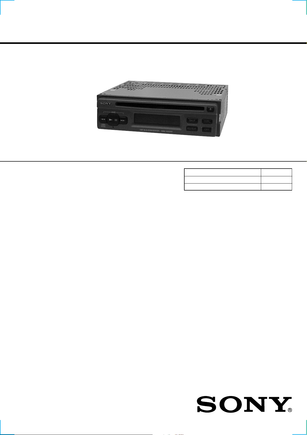
CDX-1000RF
SERVICE MANUAL
SPECIFICATIONS
AUDIO POWER SPECIFICATIONS
POWER OUTPUT AND TOTAL HARMONIC DISTORTION
13 watts per channel minimum continuous average power into
4 ohms, 4 channels driven from 20 Hz to 20 kHz with no more
than 1% total harmonic distortion.
US Model
Model Name Using Similar Mechanism CDX-2500R
CD Drive Mechanism Type MG-363X-121
Optical Pick-up Name KSS-521A
Other Specifications
CD player section
System Compact disc digital audio
system
Signal-to-noise ratio 90 dB
Frequency response 10 – 20,000 Hz
Wow and flutter Below measurable limit
Laser Diode Properties
Material GaAs+GaAlAs
Wavelength 785 – 815 nm (Typ. 800 nm)
Emission Duration Continuous
Laser output power Less than 0.5 mW*
* This output is the value measured at a distance
of 0.7 mm from the objective lens surface on the
Optical Pick-up Block.
General
Outputs Line outputs
Power requirements 12 V DC car battery
(negative ground)
Current drain 2A (at disc loading)
Dimensions Approx. 178 × 50 × 173 mm
(7 1/8 × 2 × 6 7/8 in.)
(w/h/d)
Mounting dimensions Approx. 182 × 53 × 159 mm
(7 1/4 × 2 1/8 × 6 3/8 in.)
(w/h/d)
Mass Approx. 1.1 kg (2 lb. 7 oz.)
Supplied accessories Parts for installation and
connections (1 set)
Design and specifications are subject to change without
notice.
COMPACT DISC PLAYER
1
Page 2

SERVICE NOTE
TABLE OF CONTENTS
CAUTION
Use of controls or adjustments or performance of procedures other than those specified herein may result in hazardous radiation exposure.
Notes on Chip Component Replacement
• Never reuse a disconnected chip component.
• Notice that the minus side of a tantalum capacitor may be dam-
aged by heat.
NOTES ON HANDLING THE OPTICAL PICK-UP BLOCK
OR BASE UNIT
The laser diode in the optical pick-up block may suffer electrostatic
breakdown because of the potential difference generated by the
charged electrostatic load, etc. on clothing and the human body.
During repair, pay attention to electrostatic breakdown and also use
the procedure in the printed matter which is included in the repair
parts.
The flexible board is easily damaged and should be handled with
care.
NOTES ON LASER DIODE EMISSION CHECK
The laser beam on this model is concentrated so as to be focused on
the disc reflective surface by the objective lens in the optical pickup block. Therefore, when checking the laser diode emission, observe from more than 30 cm away from the objective lens.
NOTES ON PICK-UP FLEXIBLE BOARD
The pick-up flexible board in this set is secured to the optical pickup with an adhesive tape. Once the tape is removed, an adhering
force becomes weak, and it cannot be reused.
Therefore, if the optical pick-up is replaced, replace also the pickup flexible board with a new one.
SAFETY-RELATED COMPONENT WARNING!!
COMPONENTS IDENTIFIED BY MARK 0 OR DOTTED LINE
WITH MARK 0 ON THE SCHEMATIC DIAGRAMS AND IN
THE PARTS LIST ARE CRITICAL TO SAFE OPERATION.
REPLACE THESE COMPONENTS WITH SONY PARTS WHOSE
P ART NUMBERS APPEAR AS SHOWN IN THIS MANU AL OR
IN SUPPLEMENTS PUBLISHED BY SONY.
1. GENERAL
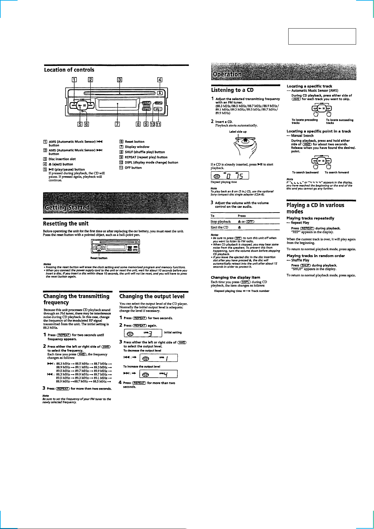
Location of controls................................................................. 3
Getting Started......................................................................... 3
Operation ................................................................................. 3
Connections ............................................................................. 4
2. DISASSEMBLY
2-1. Panel Assy, Front ................................................................. 5
2-2. CD Mechanism Block ......................................................... 5
2-3. Main Board ......................................................................... 6
2-4. Chassis (Rear) .....................................................................6
2-5. Chassis (T) Sub Assy .......................................................... 7
2-6. Lever Assy ........................................................................... 7
2-7. Servo Board......................................................................... 8
2-8. Roller Assy.......................................................................... 8
2-9. Chassis (OP) (O/S) Assy ..................................................... 9
2-10. Optical Pick-up Block ......................................................... 9
3. ELECTRICAL ADJUSTMENTS
CD Section ............................................................................10
4. DIAGRAMS
4-1. IC Pin Description............................................................. 11
4-2. Block Diagram –CD Section (1/2)– .................................. 12
4-3. Block Diagram –CD Section (2/2)– .................................. 13
4-4. Block Diagram –Display, Power Supply Section– ............ 14
4-5. Circuit Boards Location .................................................... 15
4-6. Printed Wiring Boards –CD Mechanism Section–............ 16
4-7. Schematic Diagram –CD Mechanism Section– ................ 17
4-8. Printed Wiring Board –Main Section– ..............................18
4-9. Schematic Diagram –Main Section (1/2)– ........................ 19
4-10. Schematic Diagram –Main Section (2/2)– ........................ 20
4-11. Schematic Diagram –Display Section–............................. 21
4-12. Printed Wiring Board –Display Section– ..........................22
5. EXPLODED VIEWS
5-1. Chassis Section ................................................................. 26
5-2. Front Panel Section ........................................................... 27
5-3. CD Mechanism Section (1) ............................................... 28
5-4. CD Mechanism Section (2) ............................................... 29
5-5. CD Mechanism Section (3) ............................................... 30
6. ELECTRICAL PARTS LIST ........................................ 31
2
Page 3
SECTION 1
GENERAL
This section is extracted
from instruction manual.
3
Page 4
4
Page 5
6
SECTION 2
DISASSEMBLY
Note : Follow the disassembly procedure in the numerical order given.
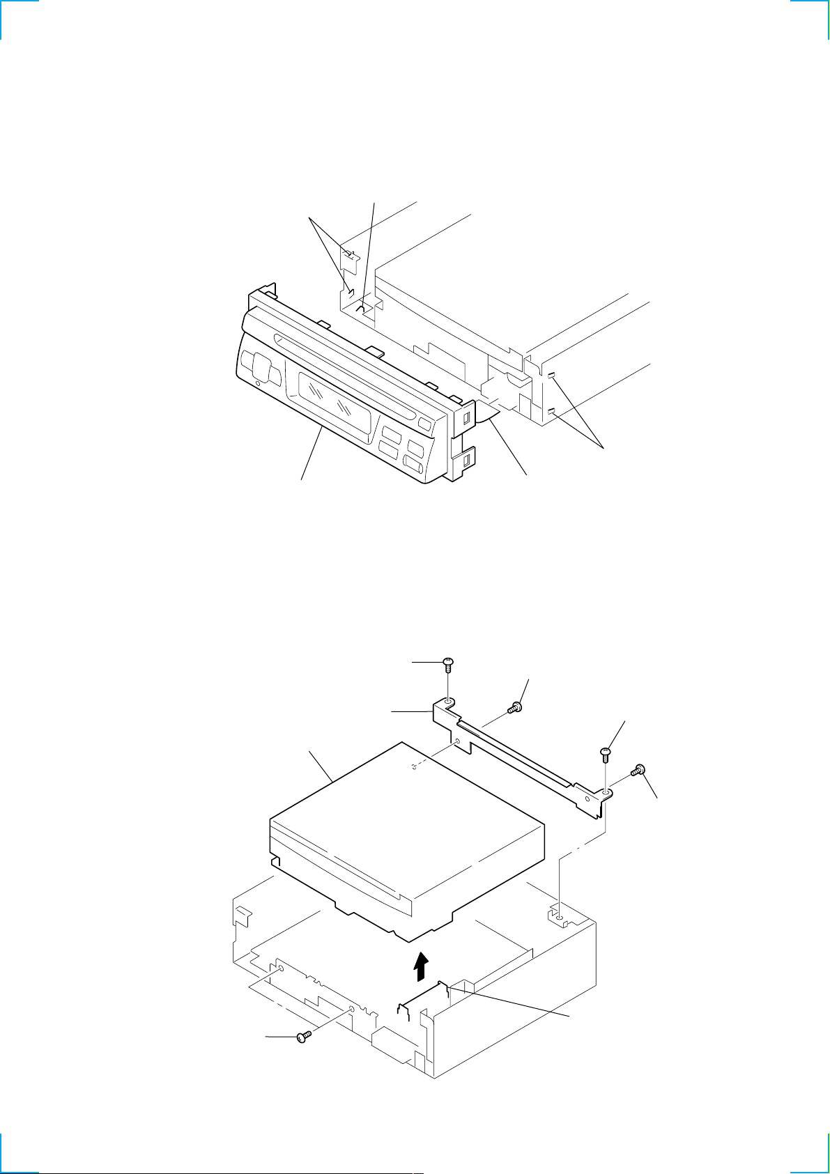
2-1. PANEL ASSY, FRONT
3 claw
2 claws
1 claws
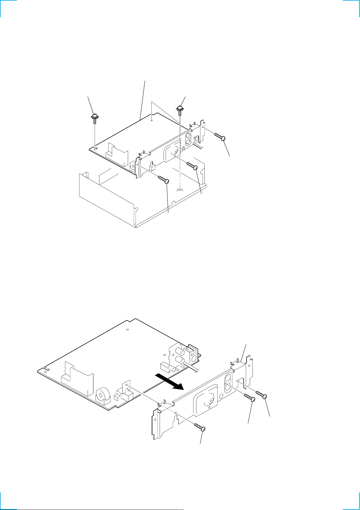
2-2. CD MECHANISM BLOCK
5 CD mechanism block
5 panel assy, front
2 PTT 2.6x6
8 bracket (M/D)
4 CNP801
7 PTT 2.6x6
3 PTT 2.6x6
6 PTT 2.6x
1 PTT 2.6x6
4 CNP701
5
Page 6
6
6
2-3. MAIN BOARD
6 MAIN board
2-4. CHASSIS (REAR)
5 ground point screw
(PTT 2.6x6)
4 ground point screws
(PTT 2.6x6)
3 PTT 2.6x
2 PTT 2.6x6
1 PTT 2.6x6
4 chassis (rear)
3 PTT 2.6x
2 PTT 2.6x6
1 PTT 2.6x6
6
Page 7
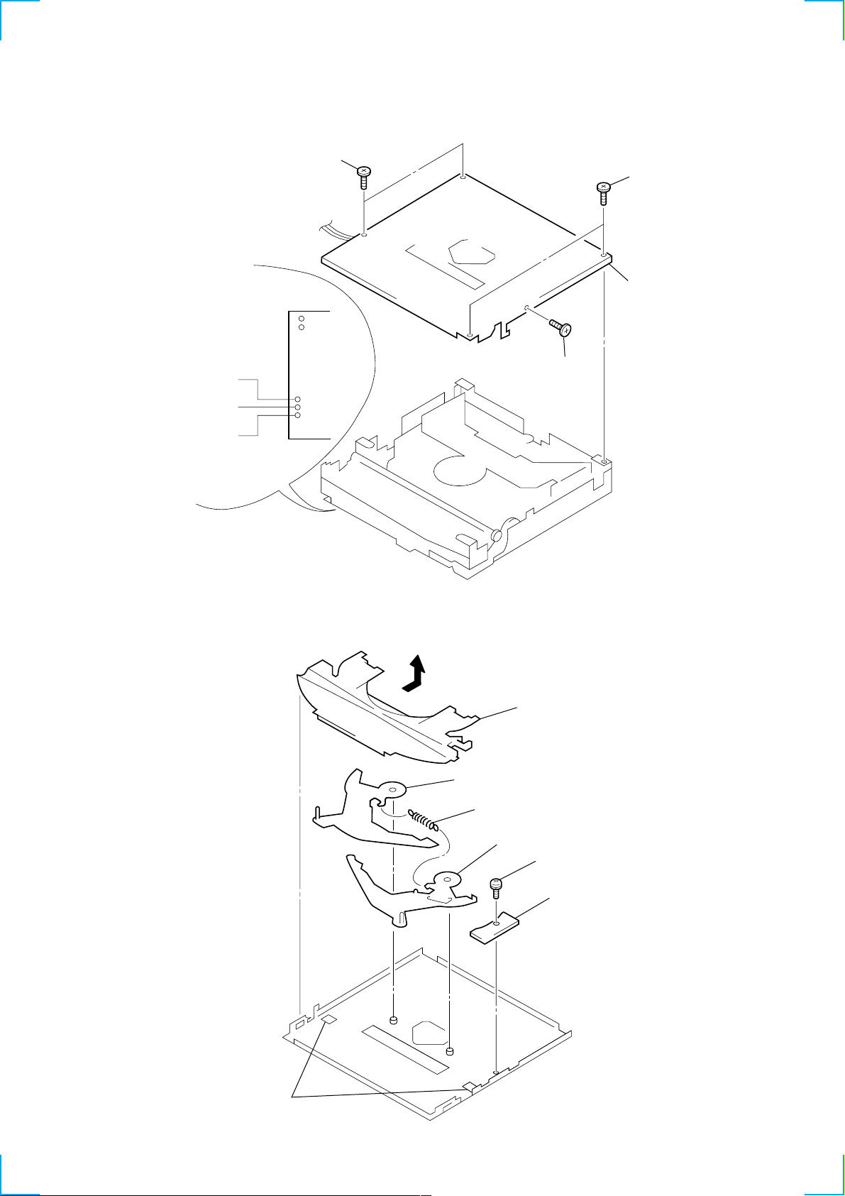
2-5. CHASSIS (T) SUB ASSY
4 P 2x3
3 P 2x3
1 Unsolder the
lead wires.
2-6. LEVER ASSY
5 chassis (T) sub assy
2 P 2x3
red
white
black
4 claws
5 guide (disc)
6 lever (R) assy
3 tension spring (LR)
7 lever (L) assy
1 PS 2x4
2 DISC IN SW board
7
Page 8
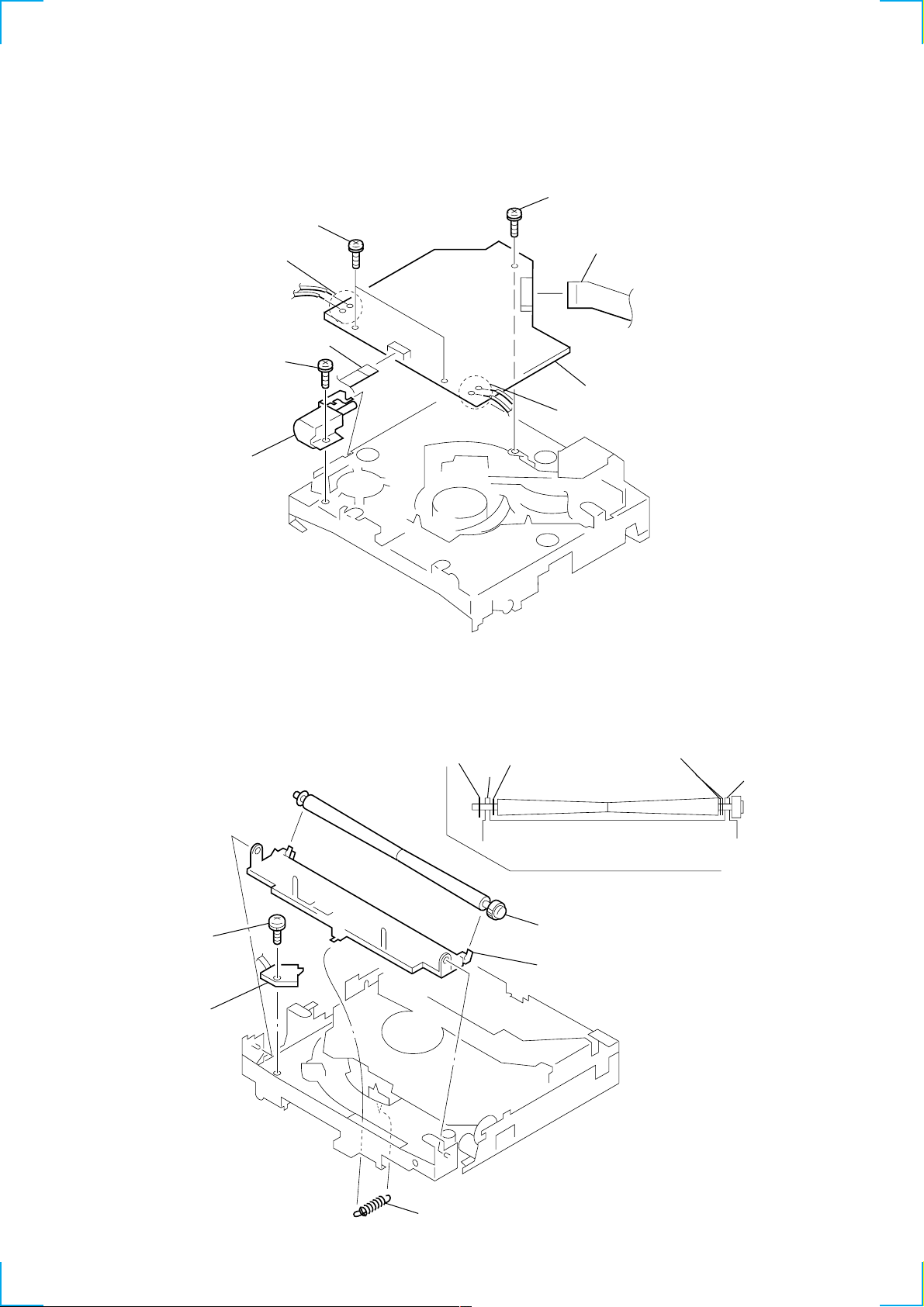
2-7. SERVO BOARD
8 PS 2x4
7 PS 2x4
3 Removal the solders.
1 CN3
5 P 2x3
6 loading motor assy
2 CN2
9 SERVO board
4 Removal the solders.
2-8. ROLLER ASSY
• When installing, take note of the positions
arm (roller) and washers. (Fig. 1)
4 PS 2x3
5 LOAD SW board
washer
ring (roller), retaining
arm
3 roller assy
2 arm (roller)
spacer, insulating
arm
Fig. 1
1 tension spring (RA)
8
Page 9
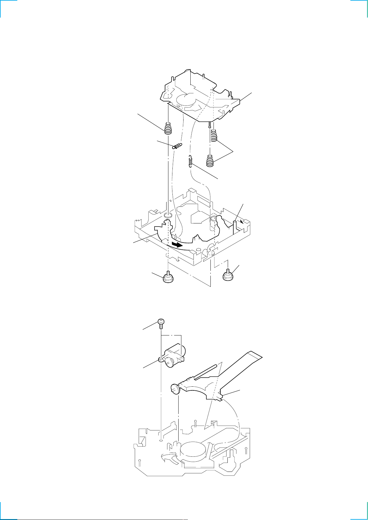
2-9. CHASSIS (OP) (O/S) ASSY
8 compression spring (FL)
1 tension spring (KF1)
7 chassis (OP) (O/S) assy
9 compression spring (FL)
2 tension spring (KR1)
5 Fit lever (D) in the
direction of the arrow.
6 Turn loading ring in the
direction of the arrow.
4 damper (T)
2-10. OPTICAL PICK-UP BLOCK
1 P 2x3
2 sled motor assy
3 damper (T)
3 optical pick-up block
9
Page 10
SECTION 3
ELECTRICAL ADJUSTMENTS
CD SECTION
Note:
1. CD Block basically constructed to operate without adjustment.
Therefore, check each item in order given.
2. Use YEDS-18 disc (3-702-101-01) unless otherwise indica ted.
3. Use the oscilloscope with more than 10 MΩ impedance.
4. Clean an objective lens by an applicator with neutral detergent
when the signal level is low than specif ied value with the f ollowing
checks.
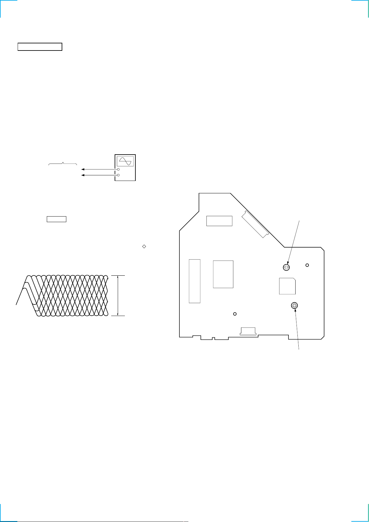
Focus Bias Adjustment
Setting: This adjustment is performed with the set placed
horizontally.
oscilloscope
SERVO board
TP (RF)
TP (RF. GND)
Procedure:
1. Connect an oscilloscope between TP (RF) and TP (RF. GND)
on the SERVO board.
2. Connect the power supply.
3. Push the RESET button (S900) on the MAIN board.
4. Insert the disc (YEDS-18) and playback.
5. Adjust RV1 so that the oscilloscope w aveform is clear and check
RF signal level is correct or not.
Note: Clear RF signal waveform means that the sharp “ ” can be
clearly distinguished at the center of the waveform.
+
–
Focus Gain Adjustment (Coarse adjustment)
This adjustment is not required unless the following parts are re placed:
• Optical pick-up
• RV4
Procedure:
1. Set RV4 to the standard position. (mechanical center)
2. Check whether operation noise (while noise type) caused by
the 2-axis device (lens section of the optical pick-up) is
abnormally loud.
If the operation noise is too loud, turn RV4 slightly counterclockwise.
• If the gain is too low:
Focus does not function and no music is selected.
• If the gain is too high:
Noise caused by scratches and dust is heard and the operation
becomes unstable.
Adjustment Location: servo board
Adjustment Location: servo board (component side)
FOCUS GAIN ADJ
IC3
CN2
RV4
RF signal waveform
VOLT/DIV: 200 mV
TIME/DIV: 500 nS
level: 1.0 – 1.5 Vp-p
• When observing the ey e pattern, set the oscilloscope to AC range
and raise the vertical sensitivity so that it may be easily seen.
Adjustment Location: servo board
CN1
IC1
TP
(RF. GND)
IC2
TP
(RF)
CN3
RV1
FOCUS BIAS ADJ
10
Page 11
SECTION 4
DIAGRAMS
4-1. IC PIN DESCRIPTION
• IC801 µPD17705GC-547-3B9 (SYSTEM CONTROL)
Pin No. Pin Name I/O Pin Description
1 NC — Not used. (Connect to ground in this set.)
2 IN_SW I Disc insertion detection input L: IN_SW
3 D_SW I DOWN switch detection input L: D_SW
4 SELF_SW I Disc self store detection input L: SELF_SW
5 L_SW I Sled limit switch detection input L: L_SW
6 LM_EJ O Loading motor control output (Eject direction)
7 LM_LD O Loading motor control output (Loading direction)
8 RY_ON O Relay control output
9, 10 NC — Not used. (Open)
11 BAND_SW I BAND select input 0: US
12 – 20 NC — Not used. (Open)
21 GND3 — Ground
22 NC — Not used. (Open)
23 ADKI2 I A/D key input 2
24 ADKI1 I A/D key input 1
25 ROTCOM I Rotary commander shift key input
26 NC — Not used. (Open)
27 TEST_SW I Test mode initial setting detection input L: TEST_SW
28, 29 NC — Not used. (Open)
30 VDD2 — Power supply pin (+5 V)
31 FMIN I PLL local oscillator frequency input
32 NC — Not used. (Open)
33 GND2 — Ground
34 NC — Not used. (Open)
35 EO1 O PLL error 1 output
36 TEST0 — Connect to GND line.
37 – 40 NC — Not used. (Open)
41 ACC_IN I Accessory power detection input L: ACC_IN
42 SCOR I SCOR signal detection input
43 MUTE O Mute control output
44 LEVEL D O Level control output
45 NC — Not used. (Open)
46 PH2 I Connect to +5 V line.
47 LEVEL 1 O Volume control output
48, 49 NC O Not used. (Open)
50 EMPH_O O Emphasis control output
51 PW_ON O System power control output
52 LM_ON O Loading motor power control output
53 CD_ON O CD power control output
54 ILLON O Illumination power control output
55 – 57 NC — Not used. (Open)
58 LCD_CE O LCD chip enable output
59 EZ_SEL I Rotary commander shift key input L: EZ_SEL
60 SENS I CD SENS signal detection input
61 FOK I Focus OK signal detection input
62 LD_ON O Laser ON/OFF control output L: LD_ON
63, 64 NC — Not used. (Open)
65 LCD_CLK O LCD serial clock output
66 LCD_DAT O LCD serial data output
67 LCD_INH O LCD inhibition output L: LCD_INH
68 SQCK0 O Sub Q read clock output
Pin No. Pin Name I/O Pin Description
69 CD_RST O Reset output to CD signal processor IC.
70 SQ_SI I Sub Q data input
71 CD_SO0 O CD signal serial data output
72 CD_LAT O CD signal processing data latch output
73 CD_CK0 O CD signal processing serial clock output
74 NC — Not used. (Open)
75 GND1 — Ground
76 XOUT O ceramic oscillator output (4.5 MHz)
77 XIN I ceramic oscillator input (4.5 MHz)
78 BU_IN I Backup power detection input
79 VDD1 — Power supply pin (+5 V)
80 RESET I Reset input L: RESET
11 11
Page 12
CDX-1000RF
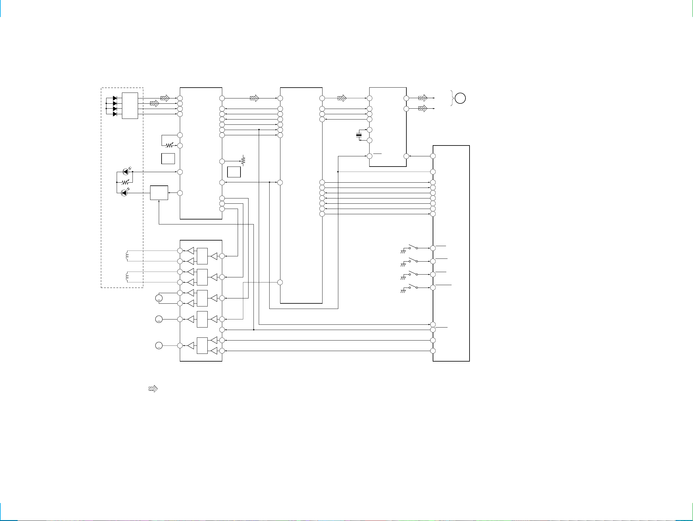
4-2. BLOCK DIAGRAM — CD SECTION (1/2) —
OPTICAL PICK-UP
KSS-521A
I-V
AMP
PD
LD
TRACKING
FOCUS
M902
(SLED)
LD POWER
CONTROL
Q1, 2
M
RF AMP, SERVO CONTROL
PD1 RF
35 31
PD2
36
E
39
F
38
FEO
1
FEI
2
RV4
FOCUS
GAIN
PD
34
LD
33
FOCUS/TRACKING COIL DRIVE,
CH2+
16
CH2–
15
CH1+
18
CH1–
17
CH3+
13
CH3–
14
IC2
FE BIAS
MOTOR DRIVE
IC3
LEVEL
SHIFT
LEVEL
SHIFT
LEVEL
SHIFT
RF 0
CLK
19
XLT
20
DATA
21
SENS
24
FOK
25
C. OUT
23
37
RV1
FOCUS
BIAS
XRST
22 50
SL O
16
FE O
6
TA O
13
CH2 IN
22
CH1 IN
19
CH3 IN
24
DIGITAL SIGNAL PROCESSOR
14
59
57
56
54
1
55
3
CLKO
XLTO
DATO
SEIN
FOK
CNIN
XRST
MDP
IC1
PCMD
BCK
LRCK
XTAI
SENS
SQSO
SQCK
DATA
XLAT
CLOK
SCOR
D/A CONVERTER
IC701
CD
DIN
21
22
20
34
X701
16.9344MHz
49
46
47
51
52
53
43
5
BCKIN
6
LRCIN
4
CLKO
19
XTI
1
XTO
20
RSTB
15
VOUTL
VOUTR
MC/DM1
SW3
(LIMIT)
SW1
(DISC IN)
SW4
(DOWN)
SW2
(SELF)
12
9
17
CD L-CH
CD R-CH
SYSTEM CONTROL
IC801 (1/3)
50
EMPH_O
69
CD_RST
60
SENS
70
SQ_SI
68
SQCK0
71
CD_SO0
72
CD_LAT
73
CD_CK0
42
SCOR
5
L_SW
2
IN_SW
3
D_SW
4
SELF_SW
SECTION
A
(Page 13)
(2/2)
CTL2
3
5
6
7
CH4 IN
FWD
REV
61
62
6
7
FOK
LD_ON
LM_EJ
LM_LD
M901
(SPINDLE)
M903
(LOADING)
04
CH4+
M
M
CH5+
12
10
LEVEL
SHIFT
LEVEL
SHIFT
• Signal path
: CD
• R-ch : same as L-ch.
12 12
Page 13

4-3. BLOCK DIAGRAM — CD SECTION (2/2) —
(Page 12)
CD
SECTION
(1/2)
A
CD L-CH
ELECTRONIC VOLUME
IC401
2 1
L/R
VOLUME
CONTROL
Q30
L/R
LEVEL
CONTROL
Q29
MUTE
Q401
CD R-CH
-1
L
-2
R
PJ401
AUDIO OUT
VOLUME
CONTROL
Q22
CDX-1000RF
L101
2 10
LEVEL
CONTROL
MPX OUT
BALANCE
BALANCE
Q23
13
15
17
TRANSMITTER
L/R BALANCE
RV1
4.5MHz
XOUT
BUFFER
X801
Q1
MPX
IC1
L IN
18
PMUTE
Q45
MUTE
CONTROL
Q403,404
47 44 43 76 77
LEVEL 1
LEVEL D
MUTE
CD R-CH
X1
38kHz
1
R IN
OSC
6
OSC
8
SYSTEM CONTROL
IC801(2/3)
XIN
D2
DEVIATION
RV10
TUNER +5V
D1
BUFFER
AMP
Q81,82
35 31
EO1
RF AMP
Q2,3
L1
RF
RF OSC
Q21
FMIN
L2
RF OSC
BATT
RELAY
SWITCH
Q15
RELAY
CONTROL
Q16
8
D919
RY_ON
RY1
• Signal path
: CD
: FM
: AM
CNJ601
(ANTENNA IN)
CN601
(ANTENNA OUT)
• R-ch : same as L-ch.
04
13 13
Page 14

CDX-1000RF
4-4. BLOCK DIAGRAM — DISPLAY, POWER SUPPLY SECTION —
SYSTEM CONTROL
IC801 (3/3)
LCD DRIVER
IC851
LIQUID CRYSTAL
DISPLAY PANEL
LCD851
CD +5V
MD +8V
CD
+5V REG
Q904
D905
D906
BACK-UP
CHECK
Q908,911,912
CD POWER
CONTROL
Q906,918
MD
+8V REG
Q901
S881
(RESET)
MD POWER
CONTROL
Q902,914
RESET LCD_DAT
80 66
BU_IN
78
PH2
46
CD_ON
53
LM_ON
52
LCD_CLK
LCD_CE
LCD_INH INH
ILLON
ADKI1
DATA
62
65
58
67
54
24
S861-864
CLK
61
CE
60
57
LCD DRIVER
POWER
CONTROL
Q913,915
COM1
COM2
S6-S26
S28-S30
U-COM +5V
64
63
6
I
23
•
25
I
27
•
29
I
31
LCD
+B REG
Q917
24
U-COM +5V
Q910
17
16
26
I
18
•
15
I
1
PL851
D861-868
ADKI2
23
S851-854
AMP REM
+B REG
Q921
TUNER +5V
04
TUNER
+5V REG
Q907
AMP REM
POWER
CONTROL
Q922
TUNER
POWER
CONTROL
Q903,905
51
PW_ON
ACC-IN
ROTCOM
EZ_SEL
ACC
41
25
59
CHECK
Q909
D913
(REMOTE IN)
J801
CNP901
4
2
1
BATTBATT
ACC
AMP REM
14 14
Page 15

4-5. CIRCUIT BOARDS LOCATION
LOAD SW board
DISC IN SW board
DISPLAY board
SUB board
SERVO board
LIMIT SW board
MAIN board
THIS NOTE IS COMMON FOR PRINTED WIRING
BOARDS AND SCHEMATIC DIAGRAMS.
(In addition to this, the necessary note is
printed in each block.)
for schematic diagram:
• All capacitors are in µF unless otherwise noted. pF: µµF
50 WV or less are not indicated except for electrolytics
and tantalums.
• All resistors are in Ω and 1/
specified.
• % : indicates tolerance.
• C : panel designation.
Note: The components identified by mark 0 or dotted line
with mark 0 are critical for safety.
Replace only with part number specified.
• U : B+ Line.
• H : adjustment for repair.
• Power voltage is dc 14.4V and fed with regulated dc power
supply from ACC and BATT cords.
• Voltages are tak en with a V OM (Input impedance 10 MΩ).
Voltage var iations may be noted due to normal production tolerances.
• Wavefor ms are taken with a oscilloscope.
Voltage var iations may be noted due to normal production tolerances.
• Circled numbers refer to waveforms.
• Signal path.
F : FM
f : AM
J : CD
for printed wiring boards:
• X : parts extracted from the component side.
• b : Pattern from the side which enables seeing.
4
W or less unless otherwise
• Waveforms (MODE:PLAY)
1
0V
Approx. 620mVp-p
1
(FEO)
IC2
2
1.2Vp-p
ea
(RFO)
IC2
3
0V
Approx. 200mVp-p
rs
(TEO)
IC2
4
2.6Vp-p
7.6µsec
3
(MDP)
IC1
5
5.8Vp-p
22.7µsec
IC1
(LRCK)
w;
6
7
IC1
IC1
474nsec
(BCK)
ws
16.89MHz
(XTAI)
ef
5.7Vp-p
3.2Vp-p
15 15
Page 16

CDX-1000RF
4-6. PRINTED WIRING BOARDS — CD MECHANISM SECTION — • Refer to page 15 for Circuit Boards Location.
• Semiconductor
Location
Ref. No. Location
IC1 D-2
IC2 E-5
IC3 B-2
Q1 F-5
Q2 F-6
(Page 18)
16 16
Page 17

4-7. SCHEMATIC DIAGRAM — CD MECHANISM SECTION — • Refer to page 15 for Waveforms.
• Refer to page 23 for IC Block Diagrams.
CDX-1000RF
Note:
• Voltage and waveforms are dc with respect to ground
under no-signal conditions.
no mark : CD PLAY
: Impossible to measure
∗
(Page
19)
17 17
Page 18

CDX-1000RF
• Semiconductor
Location
Ref. No. Location
D1 F-13
D2 F-11
D401 A-7
D402 A-8
D901 F-1
D902 D-1
D903 H-1
D904 I-1
D905 J-2
D906 D-2
D907 C-2
D908 B-4
D912 K-3
D913 C-4
D919 D-12
4-8. PRINTED WIRING BOARD — MAIN SECTION — • Refer to page 15 for Circuit Boards Location.
IC1 E-11
IC401 C-8
IC701 F-4
IC801 I-8
Q1 E-12
Q2 G-13
Q3 F-13
Q15 E-12
Q16 D-11
Q21 G-13
Q22 G-11
Q23 G-11
Q27 C-9
Q28 C-9
Q29 A-9
Q30 A-9
Q45 E-8
Q65 E-8
Q81 F-9
Q82 F-9
Q401 C-10
Q402 C-10
Q403 B-7
Q404 A-8
Q901 G-1
Q902 F-2
Q903 C-3
Q904 H-2
Q905 C-3
Q906 G-2
Q907 E-1
Q908 D-3
Q909 C-5
Q910 J-1
Q911 J-3
Q912 J-2
Q913 I-2
Q914 F-2
Q915 J-2
Q917 K-2
Q918 G-2
Q921 B-5
Q922 C-6
(Page 22)
(Page 16)
18 18
Page 19

4-9. SCHEMATIC DIAGRAM — MAIN SECTION (1/2) — • Refer to page 21 for Waveforms.
• Refer to page 25 for IC Block Diagrams.
8
10
(Page 17)
9
CDX-1000RF
11
(Page 20)
12
(Page 21)
19 19
Note:
• Voltage is dc with respect to
ground under no-signal
condition.
no mark : CD PLAY
Page 20

CDX-1000RF
4-10. SCHEMATIC DIAGRAM — MAIN SECTION (2/2) — • Refer to page 21 for Waveforms.
• Refer to page 25 for IC Block Diagrams.
(Page 19)
13
20 20
Note:
• Voltage is dc with respect to ground under no-signal
condition.
no mark : CD PLAY
Page 21

• Waveforms (MODE:PLAY)
8
5.1Vp-p
22.7µsec
IC701
(LRCIN)
4
CDX-1000RF
4-11. SCHEMATIC DIAGRAM — DISPLAY SECTION —
9
q;
qa
qs
qd
IC701
16.9344MHz
IC701
IC701
IC801
474nsec
(BCKIN)
6
(XTO)
w;
16.89MHz
(CLKO)
ql
4.5MHz
(XOUT)
uh
(Page 19)
5.1Vp-p
4.7Vp-p
4Vp-p
2.7Vp-p
IC1
22.7µsec
(OSC)
8
4.1Vp-p
Note:
• Voltage is dc with respect to ground under no-signal
condition.
no mark : CD PLAY
21 21
Page 22

CDX-1000RF
4-12. PRINTED WIRING BOARD — DISPLAY SECTION — • Refer to page 15 for Circuit Boards Location.
(Page 18)
• Semiconductor
Location
Ref. No. Location
D851 C-5
D861 A-1
D862 B-1
D863 C-1
D864 B-3
D865 B-11
D866 B-12
D867 B-13
D868 C-3
IC851 C-7
22 22
Page 23

• IC Block Diagrams
IC1 CXD2507AQ (SERVO Board)
FOK
MON
MDP
MDS
LOCK
TEST
FILO
FILI
PCO
VSS
AVSS
CLTV
AVDD
BIAS
ASYI
ASYO
ASYE
WDCK
XLON
SPOC
SPOD
63
62
64
1
2
3
4
5
6
7
8
9
10
11
12
13
RF
14
15
16
17
18
19
SERVO AUTO
SEQUENCER
CPU
INTERFACE
14
DIGITAL
PLL
ASYMMETRY
CORRECTOR
5
20 21 22 23 24 25 26 27 293031 3228
LRCK
PCMD
BCLK
16K
RAM
GTOP
CLKO
SPOB
SPOA
58596061
5
SUB CODE
PROCESSOR
EFM
DEMODULATOR
3
ERROR
CORRECTOR
GFS
VDD
XUGF
XPCK
VDD
XLTO
RFCK
DATO
CNIN
5455
5657
4
D/A
INTERFACE
3
C2PO
XROF
SEIN
53
6
MNT3
CLOK
52
MNT1
XLAT
DIGITAL
CLV
DIGITAL
OUT
CLOCK
GENERATOR
51
DATA
50
XRST
49
SENS
48
MUTE
47
SQCK
SQSO
46
45
EXCK
44
SBSO
43
SCOR
42
VSS
41
WFCK
40
EMPH
39
DOUT
C4M
38
37
FSTT
36
XTSL
35
XTAO
34
XTAI
MNTO
33
IC3 BA6796FP-T1
OP IN –
OP IN +
VREF
CH3
28
1
OPOUT
26
27
THERMAL
CTL1 CTL2 FWD REV
23 4
CH4
CH4-IN
CTL1
SHUT
DOWN
5
2425
CTL2
CH3-IN
LEVEL
SHIFT
LOGIC
CH2
23
78
6
FWD
REV
22
CH2-IN
LEVEL
SHIFT
V/I
TRAY
21
VCC
LEVEL
SHIFT
9
VCC
GND
DRIVE
BUFFER
10
CH1
CH5 –
1920
CH1-IN
DRIVE
BUFFER
DRIVE
BUFFER
11
CH1 +
LEVEL
SHIFT
COM
CH1 –
DRIVE
BUFFER
DRIVE
BUFFER
12 13
CH4 +
161718
DRIVE
BUFFER
DRIVE
BUFFER
CH2 +
CH3 +
15
DRIVE
BUFFER
DRIVE
BUFFER
14
CH2 –
CH3 –
23
Page 24

IC2 CXA1782BQ
FE BIAS
PHD 2
36 35 34
37
F
38
E
39
PHD 1
RF IV AMP1
APC
RF IV AMP2
F IV AMP
PHD
33
FE AMP
LD
RF M
32
LEVEL S
FOK
RF O
31
TTL
IIL
FZC COMP
RF I
30 29 28 27 26 25
MIRR
IIL DATA REGISTER
TOG1-3
FS1-4 TG1-2 TM1-7 PS1-4
BAL1-3
CP
CB
DFCT
INPUT SHIFT REGISTER
ADDRESS DECODER
OUTPUT DECODER
CC1
TTL
TTL
FOK
CC2
IIL
24
SENS
23
C.OUT
22
XRST
21
DATA
20
IIL
XLT
19
CLK
VCC
18
VEE
TED
LPFI
TEI
ATSC
TZC
TDFCT
BAL2
BAL 3
TOG1
TOG2
WINDOW COMP
E IV AMP
TOG3
ATSC
TE AMP
HPF COMP
TZC COMP
DFCT
TM1
DFCT
FS4
2
1
FEI
FEO
FDFCT
43
FGD
LPF COMP
TG1
FCS PHASE
COMPENSATION
5
6
FLB
FE O
FS1
FS2
FE M
TRACKING
PHASE
COMPENSATION
TM6
TM5
TM4
TM3
TM7
TG2
987
TGU
SRCH
ISET
TM2
12
TA M
17
SL O
16
SL M
15
SL P
14
13
TA O
ISET
F SET
11
10
TG2
FSET
EI
40
BAL1
41
42
43
44
45
46
47
VC
48
24
Page 25

IC1 BA1405F-E2 (MAIN Board)
L IN
18 17 16 15 14 13 12 11 10
L
AMP
R
AMP
1 2 3 4 5 6 7 8 9
R IN
IC401 BA4558F
1
OUT1
2
–IN1
+IN1
3
1CH
BALANCE
AMP BIAS
2CH
BALANCENCVCC
MPX
NC
GND
8
VCC
OUT2
7
–IN2
6
MPX OUTNCPILOT OUT
BUFFER
BUFFER 1/2
OSC 38kHz
NC
OSC
NC
OSC
OSC BIAS
NC
VEE
4
IC701 PCM1717E-S
1
XTI
2
DGND
3
VDD
4
LRCIN
5
DIN
BCKIN
6
7
ZERO
LOWPASS FILTER
D/CR
8
9
VOUTR
10
AGND
INPUT
INTERFACE
DIGITAL
FILTER
NOISE SHAPER
5LEVE DAC
CMOS
AMP
5
CLK
CONTROL
LOWPASS FILTER
+IN2
MODE
CONT
ROL
5LEVEL DAC
CMOS
AMP
20
19
18
17
16
15
14
13
12
11
XTO
CLKO
ML/MUTE
MC/DM1
MD/DM0
RSTB
MODE
D/CL
VOUTL
AVCC
25
Page 26

NOTE:
• The mechanical parts with no reference
number in the exploded views are not supplied.
• Items marked “*” are not stocked since
they are seldom required for routine service.
Some delay should be anticipated
when ordering these items.
• -XX and -X mean standardized parts, so
they may have some difference from the
original one.
5-1. CHASSIS SECTION
2
SECTION 5
EXPLODED VIEWS
• Color Indication of Appearance Parts
Example :
KNOB, BALANCE (WHITE) ... (RED)
• Accessories and packing materials and
hardware (# mark) list are given in
the last of this parts list.
F901
5
F902
R
Parts Color Cabinet’s Color
R
#1
4
3
The components identified by
mark 0 or dotted line with mark
0 are critical for safety.
Replace only with part number
specified.
#1
#1
#1
#1
MG-363X-121
#1
#1
CN601
#1
#1
7
#1
#1
10
#1
8
9
6
7
Ref. No. Part No. Description Remark
* 1 3-030-876-01 CHASSIS (MAIN)
* 2 3-030-925-41 COVER
* 3 3-024-285-01 CUSHION (RUBBER)
* 4 3-030-927-01 BRACKET (M/D)
5 1-792-738-11 CORD (WITH CONNECTOR) (POWER)
(INCLUDING F901,902)
* 6 A-3294-932-A MAIN BOARD, COMPLETE
26
1
Ref. No. Part No. Description Remark
7 3-922-535-11 SCREW (+BTT)
* 8 3-045-807-01 BRACKET (CONNECTOR)
* 9 3-043-192-01 CHASSIS (REAR)
* 10 3-030-850-01 HEAT SINK (REG)
CN601 1-792-841-11 CORD (WITH CONNECTOR) (ANTENNA OUT)
F901 1-532-798-11 FUSE (BLADE TYPE) (AUTO FUSE) (1A)
F902 1-532-731-11 FUSE (BLADE TYPE) (AUTO FUSE) (3A)
Page 27

5-2. FRONT PANEL SECTION
53
#2
55
57
58
LCD851
56
51
52
51 3-043-188-01 BUTTON (PLAY)
52 X-3378-481-1 PANEL ASSY, FRONT
53 3-043-190-01 BUTTON (AMS)
54 3-043-189-01 BUTTON (EJECT)
* 55 A-3294-933-A DISPLAY BOARD, COMPLETE
54
Ref. No. Part No. Description RemarkRef. No. Part No. Description Remark
* 56 3-043-193-01 PLATE (LCD), GROUND
* 57 3-043-196-01 SHEET (D)
* 58 X-3378-707-1 HOLDER (LCD) ASSY
LCD851 1-803-904-21 DISPLAY PANEL, LIQUID CRYSTAL
27
Page 28

5-3. CD MECHANISM SECTION (1)
(MG-363X-121)
102
104
111
112
103
#4
107
#4
#4
101
C
#3
108
109
110
105
106
114
115
111
112
113
C
M903
#5
#3
116
#3
Ref. No. Part No. Description Remark Ref. No. Part No. Description Remark
* 101 1-659-836-11 DISC IN SW BOARD
* 102 A-3291-816-B CHASSIS (T) SUB ASSY
103 3-931-909-01 SPRING (LR), TENSION
104 X-3371-501-5 LEVER (L) ASSY
105 3-338-737-01 SCREW (2X3), +PS
* 106 1-659-837-11 LOAD SW BOARD
107 X-3371-502-4 LEVER (R) ASSY
108 A-3301-203-A ROLLER ASSY
109 3-931-908-01 GUIDE (DISC)
110 3-017-301-01 ARM (ROLLER)
111 3-936-756-01 ROLLER (D)
112 3-321-393-01 WASHER, STOPPER
* 113 3-939-139-01 SPACER
114 3-931-916-01 SPRING (RA), TENSION
* 115 A-3309-227-A SERVO BOARD, COMPLETE
* 116 3-007-530-01 BRACKET (MOTOR)
M903 A-3291-676-A MOTOR SUB ASSY, LOADING (LOADING)
#4
28
Page 29

5-4. CD MECHANISM SECTION (2)
(MG-363X-121)
155
#5
154
157
158
162
166
163
D
160
166
165
164
151
156
157
153
161
D
159
152
152
152
Ref. No. Part No. Description Remark Ref. No. Part No. Description Remark
151 3-931-893-01 ARM, CHUCKING
152 3-931-897-01 DAMPER (T)
153 3-931-879-02 LEVER (D)
* 154 3-913-404-11 RETAINER (DISC)
155 3-931-894-01 BRACKET (CP)
156 3-931-895-01 SPRING (CH), TENSION
157 3-931-898-01 SPRING (FL), COMPRESSION
158 3-032-483-02 SPRING (KF1), TENSION
159 A-3277-802-C CHASSIS (M) COMPLETE ASSY
160 3-931-883-01 SPRING (TR), TENSION
161 3-931-881-01 LEVER (LOCK)
162 3-931-882-02 GEAR (MDL)
163 3-007-537-11 WHEEL (U), WORM
164 3-032-484-01 SPRING (KR1), TENSION
165 3-014-727-01 WHEEL (LW), WORM
166 3-018-272-01 WASHER
29
Page 30

5-5. CD MECHANISM SECTION (3)
(MG-363X-121)
#6
M901
207
201
202
#5
M902
208
203
205
#7
206
209
210
#4
204
213
211
212
#4
The components identified by
mark 0 or dotted line with mark
0 are critical for safety.
Replace only with part number
specified.
Ref. No. Part No. Description Remark Ref. No. Part No. Description Remark
* 201 X-3374-022-1 CHASSIS (OP) (O/S) ASSY
202 3-931-829-01 SPRING (SL), PLATE
203 X-3371-504-1 BASE (DRIVING) ASSY
204 3-931-832-01 GEAR (SL MIDWAY)
* 205 1-659-835-12 LIMIT SW BOARD
209 3-909-607-01 SCREW
0 210 8-820-010-06 PICK-UP, OPTICAL KSS-521A/K1RP
211 3-931-834-01 SPRING (FEED), PLATE
212 1-659-881-11 PICK-UP FLEXIBLE BOARD
213 A-3291-669-A SHAFT (FEED) ASSY
206 3-338-737-01 SCREW (2X3), +PS
207 1-659-880-11 MOTOR FLEXIBLE BOARD
* 208 1-659-834-11 SUB BOARD
30
M901 X-3371-664-2 MOTOR ASSY (SPINDLE)
M902 A-3291-674-A MOTOR ASSY, SLED (SLED)
Page 31

SECTION 6
ELECTRICAL PARTS LIST
NOTE:
• Due to standardization, replacements in
the parts list may be different from the
parts specified in the diagrams or the
components used on the set.
• -XX and -X mean standardized parts, so
they may have some difference from the
original one.
• RESISTORS
All resistors are in ohms.
METAL:Metal-film resistor.
METAL OXIDE: Metal oxide-film resistor.
F:nonflammable
Ref. No. Part No. Description Remark Ref. No. Part No. Description Remark
* 1-659-836-11 DISC IN SW BOARD
****************
< SWITCH >
SW1 1-572-288-21 SWITCH, PUSH (DISC IN)
SW2 1-572-288-21 SWITCH, PUSH (SELF)
*************************************************************
* A-3294-933-A DISPLAY BOARD, COMPLETE
************************
X-3378-707-1 HOLDER (LCD) ASSY
* 3-043-193-01 PLATE (LCD), GROUND
* 3-043-196-01 SHEET (D)
• Items marked “*” are not stocked since
they are seldom required for routine service.
Some delay should be anticipated
when ordering these items.
• SEMICONDUCTORS
In each case, u : µ, for example:
uA.. : µA.. uPA.. : µPA..
uPB.. : µPB.. uPC.. : µPC.. uPD.. : µPD..
• CAPACITORS
uF : µF
• COILS
uH : µH
LCD851 1-803-904-21 DISPLAY PANEL, LIQUID CRYSTAL
PL851 1-517-973-11 LAMP, PILOT
R851 1-216-057-00 METAL CHIP 2.2K 5% 1/10W
R852 1-216-057-00 METAL CHIP 2.2K 5% 1/10W
R853 1-216-057-00 METAL CHIP 2.2K 5% 1/10W
R861 1-216-057-00 METAL CHIP 2.2K 5% 1/10W
R862 1-216-057-00 METAL CHIP 2.2K 5% 1/10W
DISC IN SW DISPLAY
The components identified by
mark 0 or dotted line with mark
0 are critical for safety.
Replace only with part number
specified.
When indicating parts by reference
number, please include the board.
< LIQUID CRYSTAL DISPLAY >
< PILOT LAMP >
< RESISTOR >
< CAPACITOR >
C851 1-163-137-00 CERAMIC CHIP 680PF 5% 50V
C852 1-163-038-00 CERAMIC CHIP 0.1uF 25V
C853 1-163-117-00 CERAMIC CHIP 100PF 5% 50V
< CONNECTOR >
CN801 1-783-268-11 CABLE, FLAT
< DIODE >
D851 8-719-976-99 DIODE UDZ-TE-17-5.1B
D861 8-719-052-61 LED SLR-342PGT31 (Z)
D862 8-719-052-61 LED SLR-342PGT31 (DSPL)
D863 8-719-052-61 LED SLR-342PGT31 (OFF)
D864 8-719-052-61 LED SLR-342PGT31 (SHUF)
D865 8-719-052-61 LED SLR-342PGT31 (> (AMS))
D866 8-719-052-61 LED SLR-342PGT31 (B X)
D867 8-719-052-61 LED SLR-342PGT31 (. (AMS))
D868 8-719-052-61 LED SLR-342PGT31 (REPEAT)
< IC >
IC851 8-759-369-90 IC LC75822ED
< JUMPER RESISTOR >
R863 1-216-057-00 METAL CHIP 2.2K 5% 1/10W
R881 1-216-090-00 METAL CHIP 51K 5% 1/10W
R882 1-216-194-00 METAL CHIP 680 5% 1/8W
R884 1-216-178-00 RES-CHIP 150 5% 1/8W
R885 1-216-178-00 RES-CHIP 150 5% 1/8W
R889 1-216-043-11 RES-CHIP 560 5% 1/10W
R890 1-216-043-11 RES-CHIP 560 5% 1/10W
R891 1-216-043-11 RES-CHIP 560 5% 1/10W
R892 1-216-043-11 RES-CHIP 560 5% 1/10W
R893 1-216-043-11 RES-CHIP 560 5% 1/10W
R894 1-216-043-11 RES-CHIP 560 5% 1/10W
R895 1-216-043-11 RES-CHIP 560 5% 1/10W
R896 1-216-043-11 RES-CHIP 560 5% 1/10W
R897 1-216-043-11 RES-CHIP 560 5% 1/10W
R898 1-216-043-11 RES-CHIP 560 5% 1/10W
R899 1-216-043-11 RES-CHIP 560 5% 1/10W
R900 1-216-043-11 RES-CHIP 560 5% 1/10W
< SWITCH >
S851 1-572-704-31 SWITCH, KEY BOARD (Z)
S852 1-572-704-31 SWITCH, KEY BOARD (SHUF)
S853 1-572-704-31 SWITCH, KEY BOARD (DSPL)
S854 1-572-704-31 SWITCH, KEY BOARD (OFF)
S861 1-572-704-31 SWITCH, KEY BOARD (REPEAT)
JR805 1-216-296-00 SHORT 0
JR810 1-216-296-00 SHORT 0
JR811 1-216-296-00 SHORT 0
JR813 1-216-296-00 SHORT 0
JR814 1-216-296-00 SHORT 0
JR817 1-216-296-00 SHORT 0
JR818 1-216-296-00 SHORT 0
JR819 1-216-296-00 SHORT 0
S862 1-572-704-31 SWITCH, KEY BOARD (B X)
S863 1-572-704-31 SWITCH, KEY BOARD (> (AMS))
S864 1-572-704-31 SWITCH, KEY BOARD (. (AMS))
S881 1-572-704-31 SWITCH, KEY BOARD (RESET)
*************************************************************
31
Page 32

LIMIT SW
Ref. No. Part No. Description Remark Ref. No. Part No. Description Remark
* 1-659-835-12 LIMIT SW BOARD
***************
< SWITCH >
SW3 1-572-688-11 SWITCH, PUSH (1 KEY) (LIMIT)
*************************************************************
* 1-659-837-11 LOAD SW BOARD
***************
< SWITCH >
SW4 1-572-288-21 SWITCH, PUSH (DOWN)
*************************************************************
* A-3294-932-A MAIN BOARD, COMPLETE
*********************
* 3-030-850-01 HEAT SINK (REG)
* 3-043-192-01 CHASSIS (REAR)
* 3-045-807-01 BRACKET (CONNECTOR)
7-685-792-09 SCREW +PTT 2.6X6 (S)
MAINLOAD SW
C66 1-126-160-11 ELECT 1uF 20% 50V
C67 1-164-346-11 CERAMIC CHIP 1uF 16V
C69 1-164-346-11 CERAMIC CHIP 1uF 16V
C84 1-163-021-11 CERAMIC CHIP 0.01uF 10% 50V
C85 1-124-233-11 ELECT 10uF 20% 16V
C86 1-163-021-11 CERAMIC CHIP 0.01uF 10% 50V
C87 1-163-809-11 CERAMIC CHIP 0.047uF 10% 25V
C101 1-163-005-11 CERAMIC CHIP 470PF 10% 50V
C107 1-124-259-11 ELECT 4.7uF 20% 16V
C108 1-124-259-11 ELECT 4.7uF 20% 16V
C201 1-163-005-11 CERAMIC CHIP 470PF 10% 50V
C207 1-124-259-11 ELECT 4.7uF 20% 16V
C208 1-124-259-11 ELECT 4.7uF 20% 16V
C209 1-124-472-11 ELECT 470uF 20% 10V
C401 1-124-584-00 ELECT 100uF 20% 10V
C402 1-164-346-11 CERAMIC CHIP 1uF 16V
C701 1-163-021-11 CERAMIC CHIP 0.01uF 10% 50V
C702 1-163-235-11 CERAMIC CHIP 22PF 5% 50V
C703 1-163-235-11 CERAMIC CHIP 22PF 5% 50V
C704 1-124-233-11 ELECT 10uF 20% 16V
< CAPACITOR >
C1 1-124-259-11 ELECT 4.7uF 20% 16V
C2 1-163-009-11 CERAMIC CHIP 0.001uF 10% 50V
C3 1-163-227-11 CERAMIC CHIP 10PF 0.5PF 50V
C4 1-163-251-11 CERAMIC CHIP 100PF 5% 50V
C5 1-163-021-11 CERAMIC CHIP 0.01uF 10% 50V
C6 1-163-251-11 CERAMIC CHIP 100PF 5% 50V
C7 1-163-227-11 CERAMIC CHIP 10PF 0.5PF 50V
C8 1-163-227-11 CERAMIC CHIP 10PF 0.5PF 50V
C9 1-163-229-11 CERAMIC CHIP 12PF 5% 50V
C10 1-124-234-00 ELECT 22uF 20% 16V
C11 1-163-091-00 CERAMIC CHIP 8PF 50V
C12 1-163-021-11 CERAMIC CHIP 0.01uF 10% 50V
C13 1-163-243-11 CERAMIC CHIP 47PF 5% 50V
C14 1-163-243-11 CERAMIC CHIP 47PF 5% 50V
C15 1-164-004-11 CERAMIC CHIP 0.1uF 10% 25V
C20 1-163-021-11 CERAMIC CHIP 0.01uF 10% 50V
C21 1-163-231-11 CERAMIC CHIP 15PF 5% 50V
C24 1-124-584-00 ELECT 100uF 20% 10V
C30 1-164-005-11 CERAMIC CHIP 0.47uF 25V
C41 1-163-009-11 CERAMIC CHIP 0.001uF 10% 50V
C42 1-124-257-00 ELECT 2.2uF 20% 50V
C43 1-163-009-11 CERAMIC CHIP 0.001uF 10% 50V
C44 1-124-229-00 ELECT 33uF 20% 10V
C45 1-164-346-11 CERAMIC CHIP 1uF 16V
C46 1-126-160-11 ELECT 1uF 20% 50V
C47 1-164-346-11 CERAMIC CHIP 1uF 16V
C48 1-164-346-11 CERAMIC CHIP 1uF 16V
C61 1-163-009-11 CERAMIC CHIP 0.001uF 10% 50V
C62 1-124-257-00 ELECT 2.2uF 20% 50V
C63 1-163-009-11 CERAMIC CHIP 0.001uF 10% 50V
C65 1-164-346-11 CERAMIC CHIP 1uF 16V
C705 1-124-589-11 ELECT 47uF 20% 16V
C708 1-124-233-11 ELECT 10uF 20% 16V
C709 1-164-004-11 CERAMIC CHIP 0.1uF 10% 25V
C712 1-164-004-11 CERAMIC CHIP 0.1uF 10% 25V
C713 1-163-239-11 CERAMIC CHIP 33PF 5% 50V
C714 1-163-021-11 CERAMIC CHIP 0.01uF 10% 50V
C804 1-163-009-11 CERAMIC CHIP 0.001uF 10% 50V
C807 1-163-233-11 CERAMIC CHIP 18PF 5% 50V
C808 1-163-234-11 CERAMIC CHIP 20PF 5% 50V
C809 1-163-251-11 CERAMIC CHIP 100PF 5% 50V
C812 1-163-009-11 CERAMIC CHIP 0.001uF 10% 50V
C813 1-163-009-11 CERAMIC CHIP 0.001uF 10% 50V
C814 1-163-038-00 CERAMIC CHIP 0.1uF 25V
C831 1-163-038-00 CERAMIC CHIP 0.1uF 25V
C901 1-124-257-00 ELECT 2.2uF 20% 50V
C902 1-163-038-00 CERAMIC CHIP 0.1uF 25V
C903 1-124-257-00 ELECT 2.2uF 20% 50V
C904 1-110-654-11 DOUBLE LAYERS 0.047F 5.5V
C905 1-124-259-11 ELECT 4.7uF 20% 16V
C907 1-164-004-11 CERAMIC CHIP 0.1uF 10% 25V
C908 1-124-233-11 ELECT 10uF 20% 16V
C909 1-126-768-11 ELECT 2200uF 20% 16V
C911 1-124-259-11 ELECT 4.7uF 20% 16V
C912 1-124-584-00 ELECT 100uF 20% 10V
C914 1-163-038-00 CERAMIC CHIP 0.1uF 25V
C915 1-124-259-11 ELECT 4.7uF 20% 16V
C916 1-124-584-00 ELECT 100uF 20% 10V
< CONNECTOR >
CN601 1-792-841-11 CORD (WITH CONNECTOR) (ANTENNA OUT)
CNP701 1-764-617-12 PIN, CONNECTOR (PC BOARD) 30P
CNP801 1-563-614-31 CONNECTOR, FLEXIBLE 11P
* CNP901 1-691-785-11 PIN, CONNECTOR (PC BOARD) 4P
32
Page 33

MAIN
Ref. No. Part No. Description Remark Ref. No. Part No. Description Remark
< JACK >
CNJ600 1-793-598-11 JACK (ANTENNA IN)
< DIODE >
D1 8-719-058-78 DIODE HVU202A3TRF
D2 8-719-991-33 DIODE 1SS133T-77
D401 8-719-991-33 DIODE 1SS133T-77
D402 8-719-109-71 DIODE MTZJ-T-77-3.9A
D901 8-719-929-15 DIODE MTZJ-T-77-9.1B
D902 8-719-109-89 DIODE MTZJ-T-77-5.6B
D903 8-719-109-89 DIODE MTZJ-T-77-5.6B
D904 8-719-109-89 DIODE MTZJ-T-77-5.6C
D905 8-719-109-93 DIODE MTZJ-T-77-6.2B
D906 8-719-923-91 DIODE MTZJ-T-77-16A
D907 8-719-049-38 DIODE 1N5404TU
D908 8-719-200-82 DIODE 11ES2-TA1B
D912 8-719-921-80 DIODE MTZJ-T-77-11B
D913 8-719-991-33 DIODE 1SS133T-77
D919 8-719-991-33 DIODE 1SS133T-77
< IC >
IC1 8-759-393-50 IC A1405F-E2
IC401 8-759-909-71 IC BA4558F-T1
IC701 8-759-464-81 IC PCM1717E-ST2
IC801 8-759-675-96 IC uPD17705GC-547-3B9
< JACK >
J801 1-566-822-41 JACK (REMOTE IN)
L101 1-235-778-21 FILTER, LOW PASS
L201 1-235-778-21 FILTER, LOW PASS
L801 1-410-501-11 INDUCTOR 2.2uH
L901 1-416-539-11 INDUCTOR 370uH
< JACK >
PJ401 1-764-424-11 JACK, PIN 2P (AUDIO OUT)
< TRANSISTOR >
Q1 8-729-034-51 TRANSISTOR KTC3875
Q2 8-729-052-33 TRANSISTOR KTC3879
Q3 8-729-052-33 TRANSISTOR KTC3879
Q15 8-729-034-50 TRANSISTOR KTA1504
Q16 8-729-034-49 TRANSISTOR KRC104S
Q21 8-729-052-33 TRANSISTOR KTC3879
Q22 8-729-038-74 TRANSISTOR KRC110S
Q23 8-729-038-74 TRANSISTOR KRC110S
Q27 8-729-038-74 TRANSISTOR KRC110S
Q28 8-729-038-74 TRANSISTOR KRC110S
Q29 8-729-038-74 TRANSISTOR KRC110S
Q30 8-729-038-74 TRANSISTOR KRC110S
Q45 8-729-920-31 TRANSISTOR DTC343TK-T-146
Q65 8-729-920-31 TRANSISTOR DTC343TK-T-146
Q81 8-729-034-51 TRANSISTOR KTC3875
Q82 8-729-034-51 TRANSISTOR KTC3875
Q401 8-729-920-31 TRANSISTOR DTC343TK-T-146
Q402 8-729-920-31 TRANSISTOR DTC343TK-T-146
Q403 8-729-038-68 TRANSISTOR KRC103S
Q404 8-729-038-55 TRANSISTOR KRA103S
< JUMPER RESISTOR >
JR5 1-216-295-00 SHORT 0
JR6 1-216-295-00 SHORT 0
JR7 1-216-295-00 SHORT 0
JR10 1-216-296-00 SHORT 0
JR11 1-216-296-00 SHORT 0
JR12 1-216-296-00 SHORT 0
JR14 1-216-296-00 SHORT 0
JR17 1-216-296-00 SHORT 0
JR19 1-216-296-00 SHORT 0
JR21 1-216-296-00 SHORT 0
JR23 1-216-295-00 SHORT 0
JR24 1-216-296-00 SHORT 0
JR28 1-216-295-00 SHORT 0
JR31 1-216-295-00 SHORT 0
JR32 1-216-295-00 SHORT 0
JR35 1-216-296-00 SHORT 0
JR46 1-216-296-00 SHORT 0
JR922 1-216-296-00 SHORT 0
< COIL >
L1 1-419-619-11 COIL, IFT
L2 1-419-620-11 COIL, AIR-CORE
Q901 8-729-019-00 TRANSISTOR 2SD2394-G
Q902 8-729-038-55 TRANSISTOR KRA103S
Q903 8-729-038-55 TRANSISTOR KRA103S
Q904 8-729-922-62 TRANSISTOR 2SD1760F5-TLQ
Q905 8-729-038-67 TRANSISTOR KRC102S
Q906 8-729-038-55 TRANSISTOR KRA103S
Q907 8-729-019-00 TRANSISTOR 2SD2394-G
Q908 8-729-038-67 TRANSISTOR KRC102S
Q909 8-729-034-51 TRANSISTOR KTC3875
Q910 8-729-052-35 TRANSISTOR STD1664
Q911 8-729-034-51 TRANSISTOR KTC3875
Q912 8-729-034-51 TRANSISTOR KTC3875
Q913 8-729-038-67 TRANSISTOR KRC102S
Q914 8-729-038-67 TRANSISTOR KRC102S
Q915 8-729-038-55 TRANSISTOR KRA103S
Q917 8-729-052-35 TRANSISTOR STD1664
Q918 8-729-038-67 TRANSISTOR KRC102S
Q921 8-729-922-47 TRANSISTOR 2SB1184-TLR
Q922 8-729-038-67 TRANSISTOR KRC102S
< RESISTOR >
R1 1-216-107-00 METAL CHIP 270K 5% 1/10W
R2 1-216-053-00 METAL CHIP 1.5K 5% 1/10W
R4 1-216-025-11 RES-CHIP 100 5% 1/10W
33
Page 34

MAIN
Ref. No. Part No. Description Remark Ref. No. Part No. Description Remark
R5 1-216-063-11 RES-CHIP 3.9K 5% 1/10W
R6 1-216-073-00 METAL CHIP 10K 5% 1/10W
R7 1-216-073-00 METAL CHIP 10K 5% 1/10W
R8 1-216-075-00 METAL CHIP 12K 5% 1/10W
R9 1-216-198-11 RES-CHIP 1K 5% 1/8W
R332 1-216-049-11 RES-CHIP 1K 5% 1/10W
R333 1-216-073-00 METAL CHIP 10K 5% 1/10W
R401 1-216-049-11 RES-CHIP 1K 5% 1/10W
R408 1-216-073-00 METAL CHIP 10K 5% 1/10W
R409 1-216-073-00 METAL CHIP 10K 5% 1/10W
R10 1-216-073-00 METAL CHIP 10K 5% 1/10W
R11 1-216-059-00 METAL CHIP 2.7K 5% 1/10W
R12 1-216-190-00 RES-CHIP 470 5% 1/8W
R13 1-216-097-11 RES-CHIP 100K 5% 1/10W
R14 1-216-037-00 METAL CHIP 330 5% 1/10W
R15 1-216-174-00 RES-CHIP 100 5% 1/8W
R16 1-216-037-00 METAL CHIP 330 5% 1/10W
R17 1-216-043-11 RES-CHIP 560 5% 1/10W
R18 1-216-049-11 RES-CHIP 1K 5% 1/10W
R19 1-216-025-11 RES-CHIP 100 5% 1/10W
R20 1-216-041-00 METAL CHIP 470 5% 1/10W
R21 1-216-073-00 METAL CHIP 10K 5% 1/10W
R22 1-216-049-11 RES-CHIP 1K 5% 1/10W
R23 1-216-073-00 METAL CHIP 10K 5% 1/10W
R41 1-216-049-11 RES-CHIP 1K 5% 1/10W
R42 1-216-073-00 METAL CHIP 10K 5% 1/10W
R43 1-216-689-11 METAL CHIP 39K 0.5% 1/10W
R45 1-216-073-00 METAL CHIP 10K 5% 1/10W
R46 1-216-057-00 METAL CHIP 2.2K 5% 1/10W
R61 1-216-049-11 RES-CHIP 1K 5% 1/10W
R62 1-216-073-00 METAL CHIP 10K 5% 1/10W
R63 1-216-689-11 METAL CHIP 39K 0.5% 1/10W
R65 1-216-073-00 METAL CHIP 10K 5% 1/10W
R66 1-216-057-00 METAL CHIP 2.2K 5% 1/10W
R81 1-216-081-00 METAL CHIP 22K 5% 1/10W
R701 1-216-025-11 RES-CHIP 100 5% 1/10W
R702 1-216-033-00 METAL CHIP 220 5% 1/10W
R703 1-216-033-00 METAL CHIP 220 5% 1/10W
R704 1-216-033-00 METAL CHIP 220 5% 1/10W
R706 1-216-037-00 METAL CHIP 330 5% 1/10W
R707 1-216-027-00 METAL CHIP 120 5% 1/10W
R708 1-249-393-11 CARBON 10 5% 1/4W
R801 1-216-073-00 METAL CHIP 10K 5% 1/10W
R802 1-216-105-11 RES-CHIP 220K 5% 1/10W
R804 1-216-053-00 METAL CHIP 1.5K 5% 1/10W
R806 1-216-049-11 RES-CHIP 1K 5% 1/10W
R807 1-216-049-11 RES-CHIP 1K 5% 1/10W
R810 1-216-105-11 RES-CHIP 220K 5% 1/10W
R812 1-216-073-00 METAL CHIP 10K 5% 1/10W
R813 1-216-073-00 METAL CHIP 10K 5% 1/10W
R814 1-216-049-11 RES-CHIP 1K 5% 1/10W
R815 1-216-049-11 RES-CHIP 1K 5% 1/10W
R817 1-216-057-00 METAL CHIP 2.2K 5% 1/10W
R818 1-216-057-00 METAL CHIP 2.2K 5% 1/10W
R820 1-216-073-00 METAL CHIP 10K 5% 1/10W
R824 1-216-105-11 RES-CHIP 220K 5% 1/10W
R825 1-216-105-11 RES-CHIP 220K 5% 1/10W
R826 1-216-105-11 RES-CHIP 220K 5% 1/10W
R828 1-216-254-00 RES-CHIP 220K 5% 1/8W
R830 1-216-254-00 RES-CHIP 220K 5% 1/8W
R82 1-216-049-11 RES-CHIP 1K 5% 1/10W
R83 1-216-045-00 METAL CHIP 680 5% 1/10W
R85 1-216-689-11 METAL CHIP 39K 0.5% 1/10W
R101 1-216-057-00 METAL CHIP 2.2K 5% 1/10W
R102 1-216-073-00 METAL CHIP 10K 5% 1/10W
R104 1-216-097-11 RES-CHIP 100K 5% 1/10W
R105 1-216-088-00 METAL CHIP 43K 5% 1/10W
R106 1-216-065-11 RES-CHIP 4.7K 5% 1/10W
R107 1-216-088-00 METAL CHIP 43K 5% 1/10W
R108 1-216-059-00 METAL CHIP 2.7K 5% 1/10W
R109 1-216-053-00 METAL CHIP 1.5K 5% 1/10W
R110 1-216-071-00 METAL CHIP 8.2K 5% 1/10W
R119 1-216-061-00 METAL CHIP 3.3K 5% 1/10W
R201 1-216-057-00 METAL CHIP 2.2K 5% 1/10W
R202 1-216-073-00 METAL CHIP 10K 5% 1/10W
R204 1-216-097-11 RES-CHIP 100K 5% 1/10W
R205 1-216-088-00 METAL CHIP 43K 5% 1/10W
R206 1-216-065-11 RES-CHIP 4.7K 5% 1/10W
R207 1-216-088-00 METAL CHIP 43K 5% 1/10W
R208 1-216-059-00 METAL CHIP 2.7K 5% 1/10W
R209 1-216-053-00 METAL CHIP 1.5K 5% 1/10W
R210 1-216-071-00 METAL CHIP 8.2K 5% 1/10W
R219 1-216-061-00 METAL CHIP 3.3K 5% 1/10W
R831 1-216-089-11 RES-CHIP 47K 5% 1/10W
R832 1-216-073-00 METAL CHIP 10K 5% 1/10W
R833 1-216-049-11 RES-CHIP 1K 5% 1/10W
R834 1-216-049-11 RES-CHIP 1K 5% 1/10W
R901 1-216-182-00 RES-CHIP 220 5% 1/8W
R902 1-216-182-00 RES-CHIP 220 5% 1/8W
R903 1-216-190-00 RES-CHIP 470 5% 1/8W
R904 1-249-395-11 CARBON 15 5% 1/4W
R905 1-216-077-11 RES-CHIP 15K 5% 1/10W
R907 1-216-081-00 METAL CHIP 22K 5% 1/10W
R908 1-216-105-11 RES-CHIP 220K 5% 1/10W
R909 1-216-105-11 RES-CHIP 220K 5% 1/10W
R910 1-216-079-00 METAL CHIP 18K 5% 1/10W
R912 1-216-079-00 METAL CHIP 18K 5% 1/10W
R913 1-216-081-00 METAL CHIP 22K 5% 1/10W
R914 1-249-413-11 CARBON 470 5% 1/4W
R916 1-216-065-11 RES-CHIP 4.7K 5% 1/10W
R918 1-216-065-11 RES-CHIP 4.7K 5% 1/10W
R919 1-216-105-11 RES-CHIP 220K 5% 1/10W
R920 1-216-025-11 RES-CHIP 100 5% 1/10W
R921 1-216-025-11 RES-CHIP 100 5% 1/10W
R922 1-216-049-11 RES-CHIP 1K 5% 1/10W
R923 1-216-057-00 METAL CHIP 2.2K 5% 1/10W
34
Page 35

MAIN
Ref. No. Part No. Description Remark Ref. No. Part No. Description Remark
< VARIABLE RESISTOR >
RV10 1-241-761-11 RES, ADJ, CARBON 1K
RV11 1-238-019-11 RES, ADJ, CARBON 47K
< RELAY >
RY1 1-515-614-11 RELAY
C34 1-109-982-11 CERAMIC CHIP 1uF 10% 10V
C35 1-163-021-11 CERAMIC CHIP 0.01uF 10% 50V
C36 1-164-004-11 CERAMIC CHIP 0.1uF 10% 25V
C37 1-164-004-11 CERAMIC CHIP 0.1uF 10% 25V
C38 1-164-004-11 CERAMIC CHIP 0.1uF 10% 25V
C39 1-126-204-11 ELECT CHIP 47uF 20% 16V
C40 1-164-004-11 CERAMIC CHIP 0.1uF 10% 25V
SERVO
< THERMISTOR >
TH801 1-809-148-11 THERMISTOR PTH8L07AR2R0M1B510
< VIBRATOR >
X1 1-567-093-00 VIBRATOR, CRYSTAL (38kHz)
X701 1-579-345-11 VIBRATOR, CERAMIC (16.9344MHz)
X801 1-760-223-11 VIBRATOR, CRYSTAL (4.5MHz)
*************************************************************
* A-3309-227-A SERVO BOARD, COMPLETE
**********************
< CAPACITOR >
C1 1-107-823-11 CERAMIC CHIP 0.47uF 10% 16V
C2 1-163-021-11 CERAMIC CHIP 0.01uF 10% 50V
C3 1-135-145-11 TANTALUM CHIP 0.47uF 10% 35V
C4 1-163-251-11 CERAMIC CHIP 100PF 5% 50V
C5 1-164-182-11 CERAMIC CHIP 0.0033uF 10% 50V
C6 1-163-011-11 CERAMIC CHIP 0.0015uF 10% 50V
C7 1-163-809-11 CERAMIC CHIP 0.047uF 10% 25V
C9 1-164-004-11 CERAMIC CHIP 0.1uF 10% 25V
C10 1-126-206-11 ELECT CHIP 100uF 20% 6.3V
C11 1-135-259-11 TANTAL. CHIP 10uF 20% 6.3V
C12 1-163-227-11 CERAMIC CHIP 10PF 0.5PF 50V
C13 1-163-021-11 CERAMIC CHIP 0.01uF 10% 50V
C14 1-163-989-11 CERAMIC CHIP 0.033uF 10% 25V
C15 1-163-021-11 CERAMIC CHIP 0.01uF 10% 50V
C16 1-163-989-11 CERAMIC CHIP 0.033uF 10% 25V
C17 1-164-004-11 CERAMIC CHIP 0.1uF 10% 25V
C18 1-164-004-11 CERAMIC CHIP 0.1uF 10% 25V
C19 1-163-037-11 CERAMIC CHIP 0.022uF 10% 25V
C20 1-107-823-11 CERAMIC CHIP 0.47uF 10% 16V
C21 1-163-809-11 CERAMIC CHIP 0.047uF 10% 25V
C22 1-163-251-11 CERAMIC CHIP 100PF 5% 50V
C23 1-135-259-11 TANTAL. CHIP 10uF 20% 6.3V
C24 1-163-259-11 CERAMIC CHIP 220PF 5% 50V
C25 1-107-823-11 CERAMIC CHIP 0.47uF 10% 16V
C26 1-164-004-11 CERAMIC CHIP 0.1uF 10% 25V
C27 1-164-004-11 CERAMIC CHIP 0.1uF 10% 25V
C28 1-163-023-00 CERAMIC CHIP 0.015uF 5% 50V
C29 1-164-004-11 CERAMIC CHIP 0.1uF 10% 25V
C30 1-126-603-11 ELECT CHIP 4.7uF 20% 35V
C31 1-163-021-11 CERAMIC CHIP 0.01uF 10% 50V
C32 1-163-023-00 CERAMIC CHIP 0.015uF 5% 50V
C33 1-124-779-00 ELECT CHIP 10uF 20% 16V
< CONNECTOR >
CN1 1-764-616-12 HOUSING, CONNECTOR (PC BOARD) 30P
CN2 1-565-728-51 CONNECTOR, FPC 17P
CN3 1-770-347-21 CONNECTOR, FPC 6P
< IC >
IC1 8-752-372-94 IC XD2507AQ
IC2 8-752-074-34 IC XA1782BQ
IC3 8-759-354-16 IC A6796FP-T1
< JUMPER RESISTOR >
JR1 1-216-296-00 SHORT 0
JR2 1-216-296-00 SHORT 0
JR3 1-216-296-00 SHORT 0
JR4 1-216-296-00 SHORT 0
JR5 1-216-296-00 SHORT 0
JR6 1-216-296-00 SHORT 0
JR7 1-216-296-00 SHORT 0
JR8 1-216-296-00 SHORT 0
JR9 1-216-296-00 SHORT 0
JR10 1-216-296-00 SHORT 0
JR11 1-216-296-00 SHORT 0
JR12 1-216-296-00 SHORT 0
JR13 1-216-296-00 SHORT 0
JR14 1-216-296-00 SHORT 0
JR15 1-216-296-00 SHORT 0
JR16 1-216-296-00 SHORT 0
JR17 1-216-296-00 SHORT 0
JR18 1-216-296-00 SHORT 0
JR19 1-216-296-00 SHORT 0
JR20 1-216-296-00 SHORT 0
JR21 1-216-296-00 SHORT 0
JR22 1-216-296-00 SHORT 0
JR23 1-216-296-00 SHORT 0
JR24 1-216-296-00 SHORT 0
JR25 1-216-296-00 SHORT 0
JR26 1-216-296-00 SHORT 0
JR27 1-216-296-00 SHORT 0
JR28 1-216-296-00 SHORT 0
JR29 1-216-296-00 SHORT 0
JR30 1-216-296-00 SHORT 0
JR31 1-216-296-00 SHORT 0
JR32 1-216-296-00 SHORT 0
JR33 1-216-296-00 SHORT 0
JR34 1-216-296-00 SHORT 0
35
Page 36

SERVO
Ref. No. Part No. Description Remark Ref. No. Part No. Description Remark
JR35 1-216-296-00 SHORT 0
JR36 1-216-296-00 SHORT 0
JR37 1-216-296-00 SHORT 0
JR38 1-216-296-00 SHORT 0
JR39 1-216-296-00 SHORT 0
SUB
R36 1-216-097-11 RES-CHIP 100K 5% 1/10W
R37 1-216-117-00 METAL CHIP 680K 5% 1/10W
R38 1-216-109-00 METAL CHIP 330K 5% 1/10W
R39 1-216-101-00 METAL CHIP 150K 5% 1/10W
R40 1-216-114-00 RES-CHIP 510K 5% 1/10W
JR40 1-216-296-00 SHORT 0
JR41 1-216-296-00 SHORT 0
JR43 1-216-296-00 SHORT 0
JR44 1-216-296-00 SHORT 0
JR45 1-216-296-00 SHORT 0
JR46 1-216-296-00 SHORT 0
< COIL >
L1 1-412-058-11 INDUCTOR CHIP 10uH
L2 1-412-058-11 INDUCTOR CHIP 10uH
L3 1-412-058-11 INDUCTOR CHIP 10uH
< TRANSISTOR >
Q1 8-729-904-60 TRANSISTOR DTB113ZK-T-146
Q2 8-729-904-86 TRANSISTOR 2SB1197K-T-146-Q
< RESISTOR >
R1 1-216-073-00 METAL CHIP 10K 5% 1/10W
R2 1-216-097-11 RES-CHIP 100K 5% 1/10W
R3 1-216-121-11 RES-CHIP 1M 5% 1/10W
R4 1-216-061-00 METAL CHIP 3.3K 5% 1/10W
R5 1-216-061-00 METAL CHIP 3.3K 5% 1/10W
R6 1-216-073-00 METAL CHIP 10K 5% 1/10W
R7 1-216-009-11 RES-CHIP 22 5% 1/10W
R8 1-216-119-00 METAL CHIP 820K 5% 1/10W
R9 1-216-119-00 METAL CHIP 820K 5% 1/10W
R10 1-216-073-00 METAL CHIP 10K 5% 1/10W
R11 1-216-073-00 METAL CHIP 10K 5% 1/10W
R14 1-216-085-00 METAL CHIP 33K 5% 1/10W
R15 1-216-085-00 METAL CHIP 33K 5% 1/10W
R16 1-216-077-11 RES-CHIP 15K 5% 1/10W
R17 1-216-081-00 METAL CHIP 22K 5% 1/10W
R19 1-216-079-00 METAL CHIP 18K 5% 1/10W
R20 1-216-105-11 RES-CHIP 220K 5% 1/10W
R21 1-216-105-11 RES-CHIP 220K 5% 1/10W
R22 1-216-085-00 METAL CHIP 33K 5% 1/10W
R23 1-216-121-11 RES-CHIP 1M 5% 1/10W
R24 1-216-073-00 METAL CHIP 10K 5% 1/10W
R27 1-216-295-00 SHORT 0
R28 1-216-101-00 METAL CHIP 150K 5% 1/10W
R29 1-216-097-11 RES-CHIP 100K 5% 1/10W
R30 1-216-097-11 RES-CHIP 100K 5% 1/10W
R41 1-216-093-11 RES-CHIP 68K 5% 1/10W
R42 1-216-103-00 METAL CHIP 180K 5% 1/10W
R43 1-216-097-11 RES-CHIP 100K 5% 1/10W
R44 1-216-085-00 METAL CHIP 33K 5% 1/10W
R45 1-216-081-00 METAL CHIP 22K 5% 1/10W
R45 1-216-089-11 RES-CHIP 47K 5% 1/10W
R46 1-216-097-11 RES-CHIP 100K 5% 1/10W
R47 1-216-105-11 RES-CHIP 220K 5% 1/10W
R48 1-216-073-00 METAL CHIP 10K 5% 1/10W
R49 1-216-065-11 RES-CHIP 4.7K 5% 1/10W
R50 1-216-065-11 RES-CHIP 4.7K 5% 1/10W
R51 1-216-295-00 SHORT 0
< CERMET RESISTOR >
RV1 1-238-091-11 RES, ADJ, CERMET 22K
RV4 1-238-091-11 RES, ADJ, CERMET 22K
*************************************************************
* 1-659-834-11 SUB BOARD
**********
< CONNECTOR >
CN1 1-770-347-21 CONNECTOR, FPC 6P
*************************************************************
MISCELLANEOUS
***************
5 1-792-738-11 CORD (WITH CONNECTOR) (POWER)
207 1-659-880-11 MOTOR FLEXIBLE BOARD
0 210 8-820-010-06 PICK-UP, OPTICAL KSS-521A/K1RP
212 1-659-881-11 PICK-UP FLEXIBLE BOARD
F901 1-532-798-11 FUSE (BLADE TYPE) (AUTO FUSE) (1A)
F902 1-532-731-11 FUSE (BLADE TYPE) (AUTO FUSE) (3A)
M901 X-3371-664-2 MOTOR ASSY (SPINDLE)
M902 A-3291-674-A MOTOR ASSY, SLED (SLED)
M903 A-3291-676-A MOTOR SUB ASSY, LOADING (LOADING)
*************************************************************
ACCESSORIES & PACKING MATERIALS
********************************
3-045-044-11 MANUAL, INSTRUCTION (ENGLISH)
*************************************************************
R31 1-216-081-00 METAL CHIP 22K 5% 1/10W
R32 1-216-109-00 METAL CHIP 330K 5% 1/10W
R33 1-216-105-11 RES-CHIP 220K 5% 1/10W
R34 1-216-009-11 RES-CHIP 22 5% 1/10W
R35 1-216-065-11 RES-CHIP 4.7K 5% 1/10W
36
The components identified by
mark 0 or dotted line with mark
0 are critical for safety.
Replace only with part number
specified.
Page 37

Ref. No. Part No. Description Remark
**************
HARDWARE LIST
**************
#1 7-685-792-09 SCREW +PTT 2.6X6 (S)
#2 7-685-105-19 SCREW +P 2X8 TYPE2 NON-SLIT
#3 7-628-253-00 SCREW +PS 2X4
#4 7-627-553-37 SCREW, PRECISION +P 2X3 TYPE3
#5 7-627-553-17 SCREW, PRECISION +P 2X2 TYPE3
#6 7-627-000-00 SCREW, PRECISION +P 1.7X2.2 TYPE3
#7 7-627-850-28 SCREW, PRECISION +P 1.4X3
*************************************************************
PARTS FOR INSTALLATION AND CONNECTIONS
***************************************
251 3-014-370-21 FRAME, FITTING
252 3-916-012-01 BRACKET (ND), FITTING ASSIST
253 7-682-160-01 SCREW +P 4X6
254 X-3368-725-1 SCREW ASSY, FITTING
255 X-3378-482-1 COLLAR ASSY
256 3-931-977-01 BRACKET
257 3-934-325-01 SCREW (+K 5X8 TP)
258 1-792-738-11 CORD (WITH CONNECTOR) (POWER)
* 259 3-035-161-01 BRACKET (RELEASE)
(INCLUDING F901,902)
251
255
252
256 257
258 259
254
253
37
Page 38

CDX-1000RF
9-870-139-11
38
Sony Corporation
Mobile Electronics Division Company
Printed in Japan ©2000. 3
2000C0416-1
Published by General Engineering Dept.
 Loading...