Sony CDPX-5000 Service manual
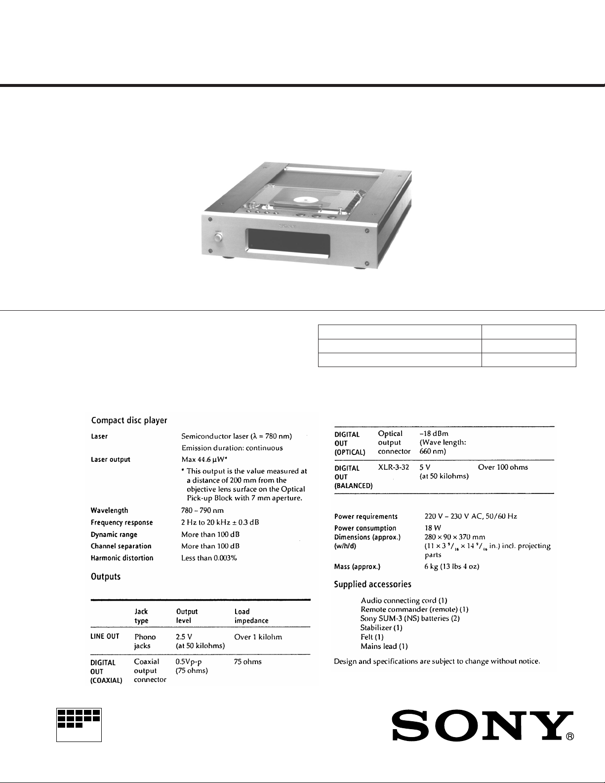
CDP-X5000
SERVICE MANUAL
Model Name Using Similar Mechanism NEW
Base Unit Type BU-12A
Optical Pick-up Type KSS-274A/J-N
SPECIFICATIONS
AEP Model
UK Model
E Model
Chinese Model
MICROFILM
General
COMPACT DISC PLAYER
— 1 —
CAUTION
Use of controls or adjustments or performance of procedures
other than those specified herein may result in hazardous radiation exposure.
TABLE OF CONTENTS
1. SERVICING NOTE ........................................................... 3
2. GENERAL ........................................................................... 4
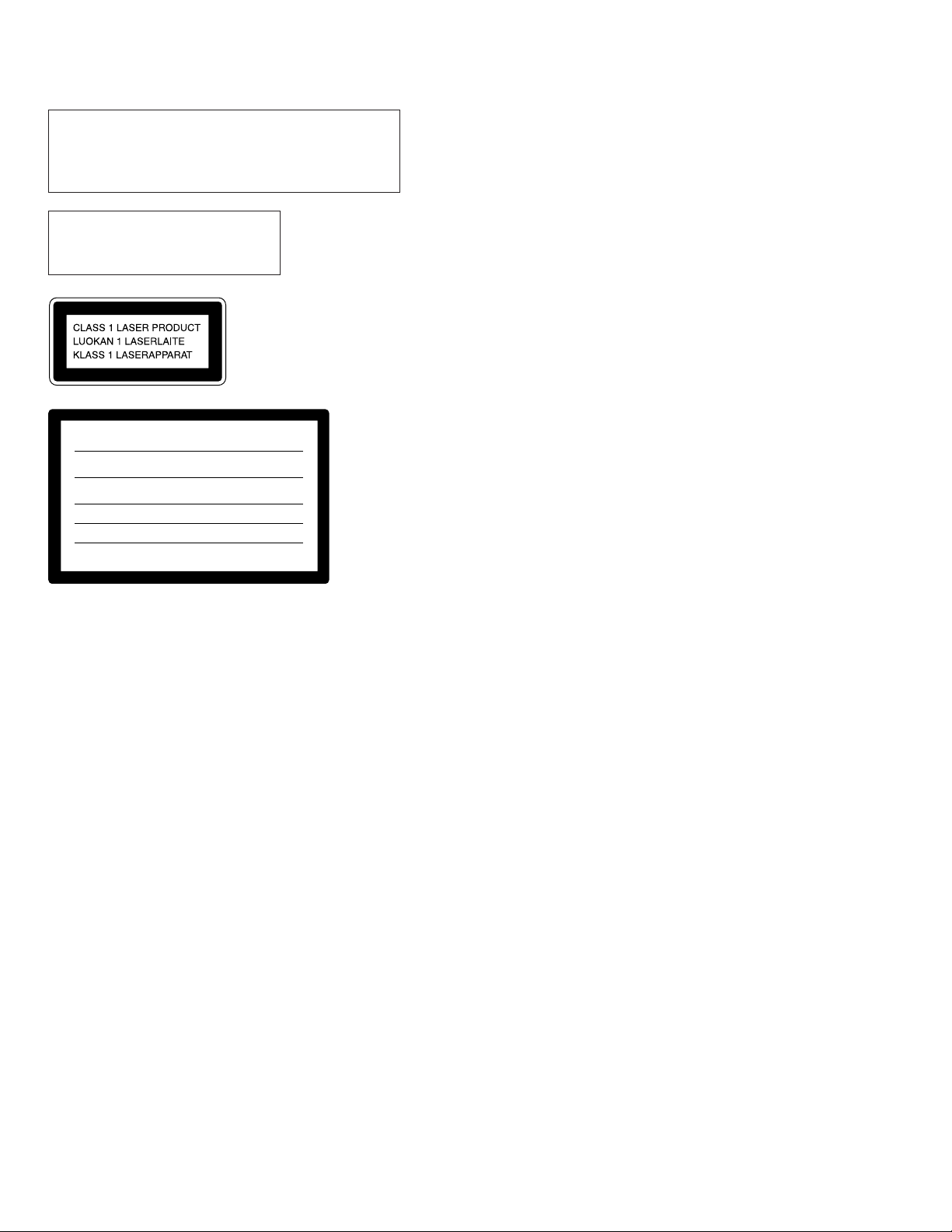
The laser component in this product
is capable of emitting radiation
exceeding the limit for Class 1.
This appliance is classified as
a CLASS 1 LASER product.
The CLASS 1 LASER
PRODUCT MARKING is
located on the rear exterior.
CAUTION
: INVISIBLE LASER RADIATION WHEN OPEN AND
INTERLOCKS DEFEATED. AVOID EXPOSURE TO BEAM.
ADVARSEL
SIKKERHEDSAFBRYDERE ER UDE AF FUNKTION. UNDGÅ UDSAETTELSE
FOR STRÅLING.
VORSICHT
ABDECKUNG GE
ÜBERBRÜCKT.
VARO!
TIINA NÄKYMÄTTÖMÄLLE LASERSÄTEILYLLE. ÄLÄ KATSO SÄTEESEEN.
VARNING
NAD OCH SPÄRREN ÄR URKOPPLAD. BETRAKTA EJ STRÅLEN.
ADVARSEL
SIKKERHEDSLÅS BRYTES. UNNGÅ EKSPONERING FOR STRÅLEN.
: USYNLIG LASERSTRÅLING VED ÅBNING NÅR
: UNSICHTBARE LASERSTRAHLUNG, WENN
Ö
FFNET UND SICHEREITSVERRIEGELUNG
NICHT DEM STRAHL AUSSETZEN.
: AVATTAESSA JA SUOJALUKITUS OHITETTAESSA OLET ALT-
: OSYNLIG LASERSTRÅLING NÄR DENNA DEL ÄR ÖPP-
: USYNLIG LASERSTRÅLING NÅR DEKSEL ÅPNES OG
This caution
label is located
inside the unit.
3. DISASSEMBLY
3-1. Top Plate Assembly ............................................................. 8
3-2. Front Panel Assembly .......................................................... 8
3-3. Base Unit ............................................................................. 9
3-4. Back Panel ........................................................................... 9
4. ELECTRICAL BLOCK ADJUSTMENTS ............... 10
5. DIAGRAMS
5-1. Circuit Boards Location .................................................... 12
5-2. IC Pin Function
• IC101 Focus/Tracking/Sled/EFM Comparator
(CXD2515AQ ) ............................................................... 13
• IC201 System Control (CXP84124-043Q) ..................... 16
5-3. Printed Wiring Board — Servo, Panel Section —............. 20
5-4. Schematic Diagram — Servo, Panel Section — ............... 23
5-5. Schematic Diagram — Audio, Power Section — ............. 28
5-6. Printed Wiring Board — Audio, Power Section —........... 31
6. EXPLODED VIEWS
6-1. Top Plate Assembly Seciton .............................................. 37
6-2. Front Panel Section ........................................................... 38
6-3. Back Panel Section ............................................................ 39
6-4. Base Unit Section (BU-12A)............................................. 40
7. ELECTRICAL PARTS LIST ..................................... 41
Notes on chip component replacement
• Never reuse a disconnected chip component.
• Notice that the minus side of a tantalum capacitor may be
damaged by heat.
Flexible Circuit Board Repairing
• Keep the temperature of soldering iron around 270˚C
during repairing.
• Do not touch the soldering iron on the same conductor of the
circuit board (within 3 times).
• Be careful not to apply force on the conductor when soldering
or unsoldering.
SAFETY-RELATED COMPONENT WARNING !!
COMPONENTS IDENTIFIED BY MARK ! OR
DOTTED LINE WITH MARK ! ON THE SCHEMATIC
DIAGRAMS AND IN THE P ARTS LIST ARE CRITICAL
TO SAFE OPERATION. REPLACE THESE COMPONENTS WITH SONY PARTS WHOSE PART NUMBERS APPEAR AS SHOWN IN THIS MANUAL OR IN
SUPPLEMENTS PUBLISHED BY SONY.
— 2 —
SECTION 1
SERVICING NOTE
NOTES ON HANDLING THE OPTICAL PICK-UP BLOCK
OR BASE UNIT
The laser diode in the optical pick-up block may suffer electrostatic
break-down because of the potential difference generated by the
charged electrostatic load, etc. on clothing and the human body.
During repair, pay attention to electrostatic break-down and also use
the procedure in the printed matter which is included in the repair
parts.
The flexible board is easily damaged and should be handled with
care.
NOTES ON LASER DIODE EMISSION CHECK
The laser beam on this model is concentrated so as to be focused on
the disc reflective surface by the objecti ve lens in the optical pick-up
block. Therefore, when checking the laser diode emission, observe
from more than 30 cm away from the objective lens.
LASER DIODE AND FOCUS SEARCH OPERA TION CHECK
Carry out the “S curve check” in “CD section adjustment” and check
that the S curve waveform is output three times.
WRITING OF FOCUS/TRACKING AUTO GAIN DATA
General CD palyers using digital servo ICs automatically adjust the
focus/tracking gain each time the disc is changed.
In this unit, the gain of the standard disc (YEDS-18) is written in the
non-volatile memory (IC203:X24C01S) of the servo board so that
the gain need not be re-adjusted when changing discs.
Therefore, if the servo board, IC203 of the servo board, or optical
pick-up has been replaced, be sure to write the auto gain data.
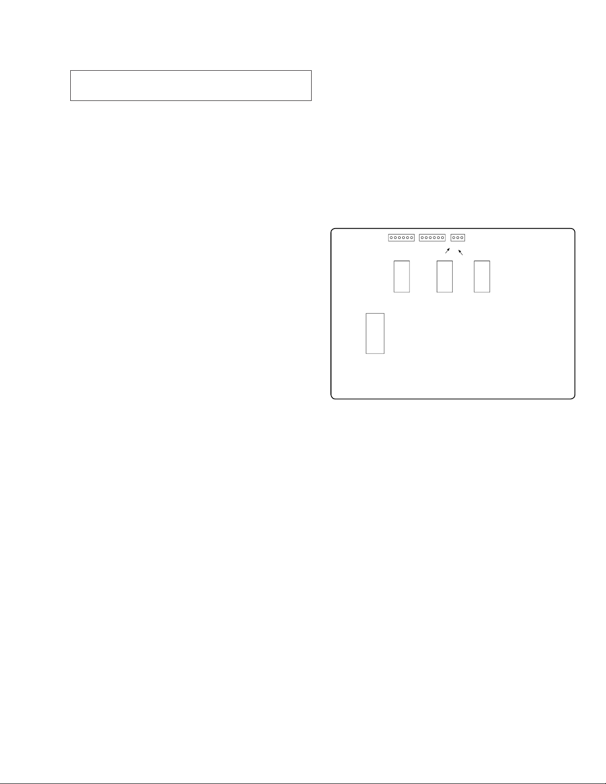
FLUORESCENT INDICA T OR TUBE FULL LIGHTING MODE
1. Connect TP (AFJ:Pin 2 of CN515) to GND (Ground), and turn
ON the POWER switch.
2. The bridge check (check for short-circut between pins of the S
RAM (IC202 of the servo board)) is performed, and all the FL
tubes light up if there is no bridge.
3. When a key other than the p(stop) key is pressed, the corresponding FL tubes lights up.
Each time the p(stop) key is pressed, all the FL tubes light up.
[SERVO BOARD] — Conductor Side —
CN515
ADJ
321
AFJ
IC102
CN514
IC104 IC105
IC202
CN513
1. Connect TP (ADJ: Pin 3 of CN515) to GND (Ground), and turn
ON the POWER switch.
2. Insert the test disc (YEDS-18). (The TOC data of the disc will be
read.)
This memorizes the auto gain data of the test disc.
Note:
• If the disc is replaced without turning OFF the power, the auto gain
data of the last disc inserted will be memorized.
• If the POWER switch is turned ON without connecting TP (ADJ)
to GND, the auto gain data will not be memorized when the disc is
inserted, and the data memorized the last time will be taken as the
focus/tracking data.
— 3 —
LOCATION OF PARTS AND CONTROLS
SECTION 2
GENERAL
This section is extracted from
instruction manual.
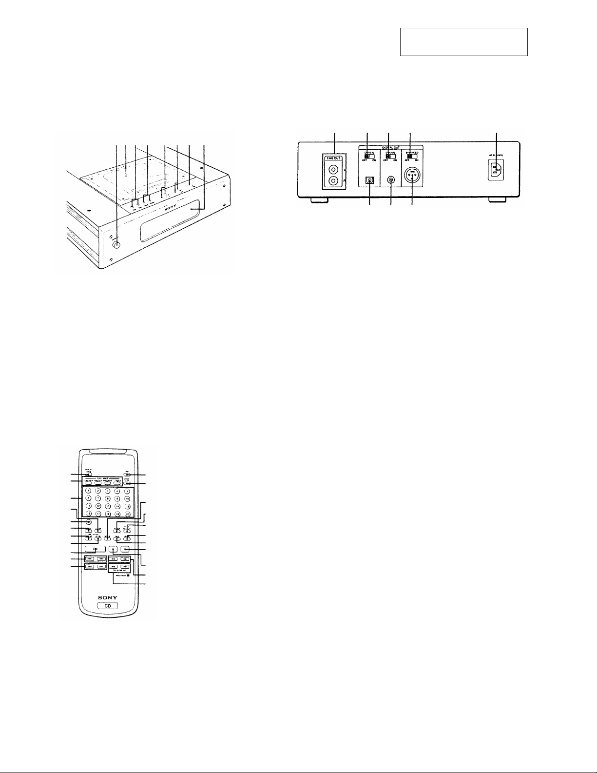
UNIT OPERATION BLOCK
123
1 POWER switch
2 Disc lid
3 0/) (fast forward/
fast rewind) buttons
4
56
8
7
5 · (play) button/lamp
6 P (pause)button/lamp
7 p (stop)button
8 Display window
4 =/+ buttons (*AMS)
*AMS is the abbreviation of Automatic Music Sensor.
REAR PANEL
1
3
87
42
6
1LINE OUT
2 DIGITAL OUT OPTICAL switch
3 DIGITAL OUT COAXIAL switch
4 DIGITAL OUT BALANCED switch
5 AC IN (230V)
6 DIGITAL OUT BALANCED
7 DIGITAL OUT COAXIAL
8 DIGITAL OUT OPTICAL
5
REMOTE COMMANDER (RM-DX5000)
1
2
3
4
5
6
7
8
9
!º
!¡
!™
!£
!¢
!∞
!§
!¶
!•
!ª
@º
@¡
@™
1 DISPLAY MODE button
2 PLAY MODE buttons
CONTINUE button
SHUFFLE button
PROGRAM button
C.INDEX button
3 Number buttons (1-20)
4 CLEAR button
5 >20 button
6 CHECK button
7 REPEAT button
8 A˜B button
9 ·(play) button
!º =/+ (*AMS) buttons
!¡ C/c(index search) buttons
!™ TIME button
!£ MUSIC SCAN button
!¢ SPACE button
!∞ FADER button
!§ PEAK SEARCH button
!¶ ERASE button
!• FILE button
!ª p (stop) button
@º P (pause) button
@¡ 0/) (fast forward/
fast rewind) buttons
@™ 0/) SLOW buttons
— 4 —
— 5 —
— 6 —
— 7 —
SECTION 3
DISASSEMBLY
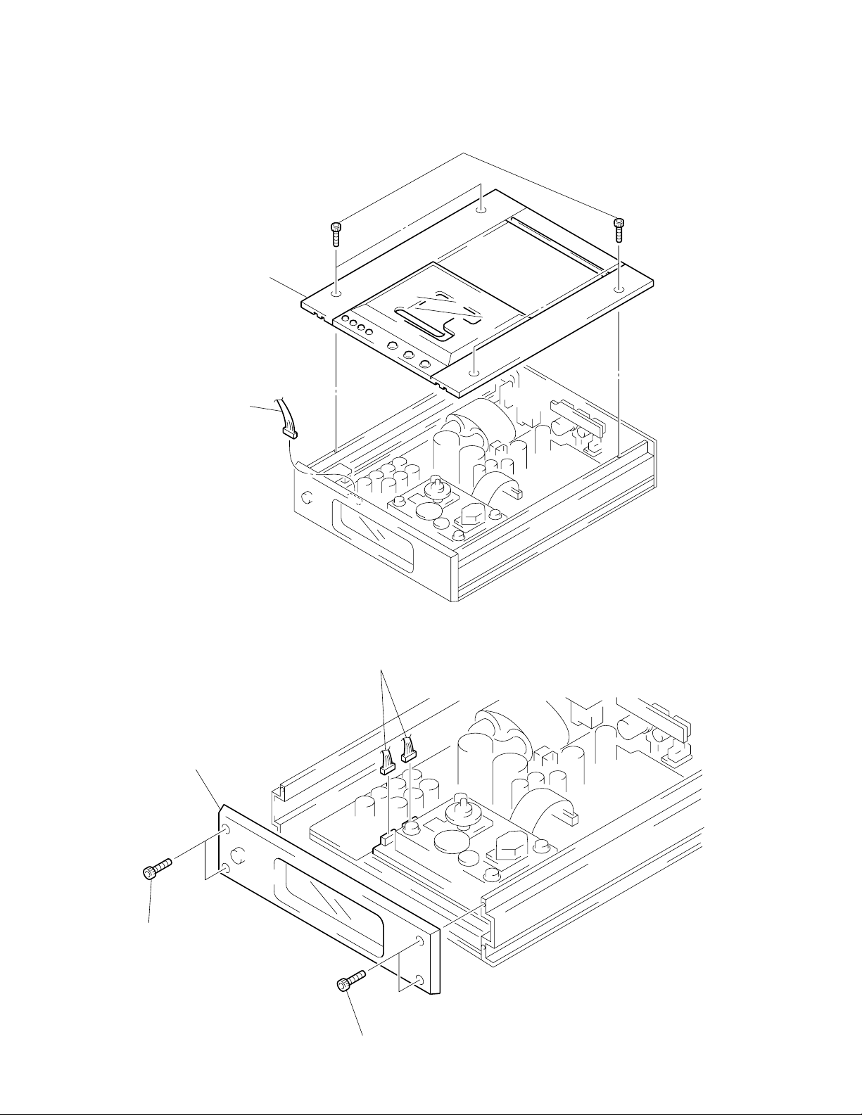
Note : Follow the disassembly procedure in the numerical order given.
3-1. TOP PLATE ASSEMBLY
2
Top plate assembly
3
Connector
(CN805: Display board)
1
Four ornamental screws
3-2. FRONT PANEL ASSEMBLY
4
Front panel assembly
2
Two bolts (M3)
1
Connectors (CN207, CN208: SERVO board)
3
Two bolts (M3)
— 8 —
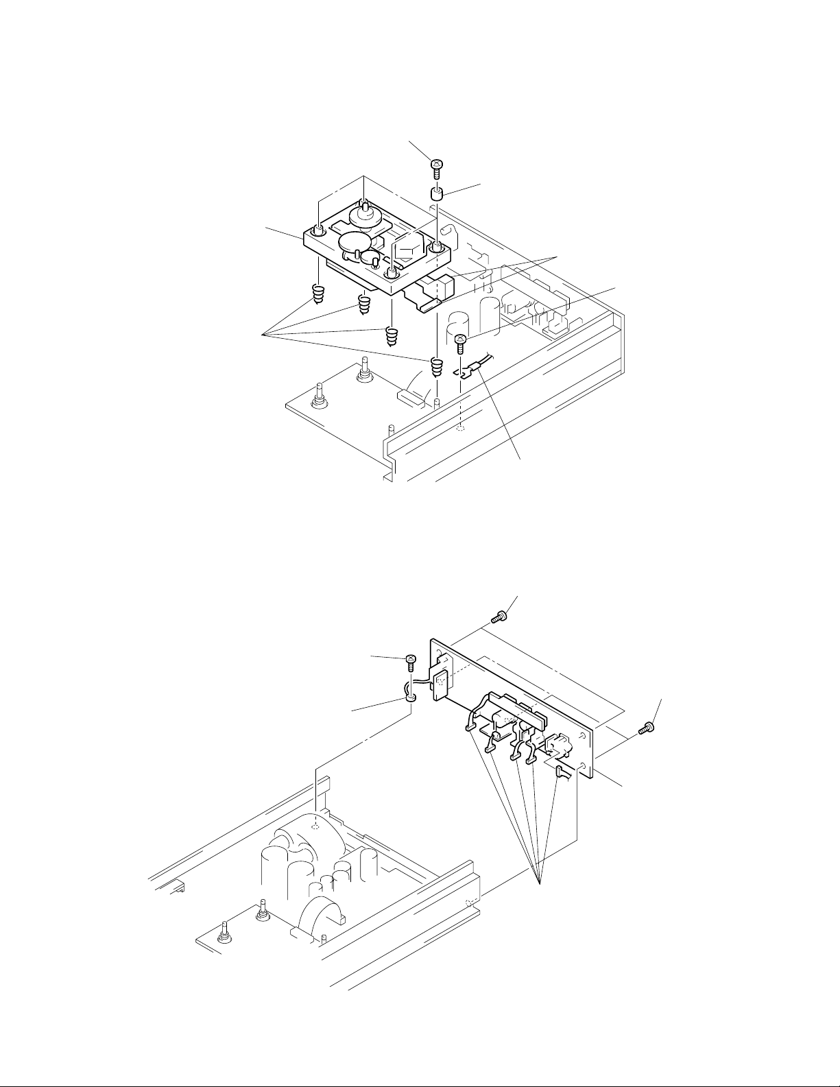
3-3. BASE UNIT
6
Base unit
Spring
4
Four screws (B 2.6X6)
5
Boss (M) (Four pieces)
1
3
Ground wire
Connectors
(CN201, CN210: SERVO board)
2
Screw (B 3X8)
3-4. BACK PANEL
2
Screw (B 3X8)
3
Ground wire
4
Two screws (B 3X6)
5
6
Back panel assembly
1
Connectors
(CN305: A OUT board)
(CN502: CN508, CN509, CN512: AUDIO board)
Three screws (BV 3X8)
— 9 —
SECTION 4
ELECTRICAL BLOCK ADJUSTMENTS
Note:
1. CD Block is basically designed to operate without adjustment.
Therefore, check each item in order given.
2. Use YEDS-18 disc (3-702-101-01) unless otherwise indicated.
3. Use an oscilloscope with more than 10MΩ impedance.
4. Clean the object lens by an applicator with neutral detergent when
the signal level is low than specified value with the following
checks.
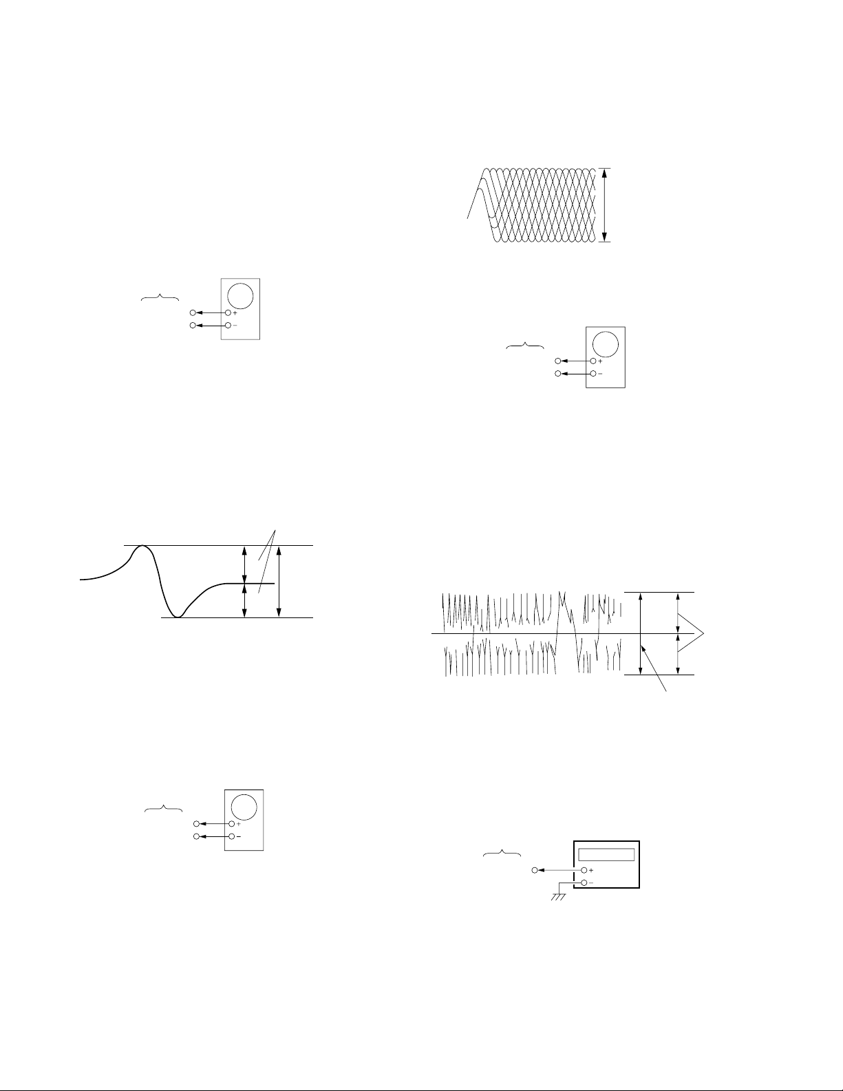
S Curve Check
oscilloscope
SERVO board
TP (FE)
TP (VC)
Procedure :
1. Connect oscilloscope to test point TP (FE: CN210 !ºpin).
2. Connect between test point TP (FEI: IC101 @ªpin) and TP (VC:
CN210 !™pin) by lead wire.
3. Put disc (YEDS-18) in and turn Power switch on and actuate the
focus search.
4. Chec k the oscilloscope waveform (S-curve) is symmetrical between A and B. And confirm peak to peak level within 3±1 Vp-p.
S-curve waveform
symmetry
Note: A clear RF signal waveform means that the shape “◊” can be
clearly distinguished at the center of the waveform.
RF signal waveform
VOLT/DIV : 200mV
TIME/DIV : 500ns
level : 1.2 Vp-p
+0.25
–0.20
E-F Balance Check
oscilloscope
SERVO board
TP (TE)
TP (VC)
Procedure :
1. Connect test point TP (ADJ: CN515 3pin) to Ground and TP
(TEI: IC101 @¶pin) to TP (VC: CN210 !™pin) with a lead wire.
2. Connect oscillscope to test point TP (TE: CN210 !¡pin)
3. Turn Power switch on.
4. Put disc (YEDS-18) in and playback.
5. Confirm that the oscilloscope waveform is symmetrical on the
top and bottom in relation to 0Vdc, and check this level.
A
level: 3 ± 1 Vp-p
B
5. After check, remove the lead wire connected in step 2.
Note : • Try to measure several times to make sure than the ratio of
A : B or B : A is more than 10 : 7.
• T ake sweep time as long as possible and light up the brightness to obtain best waveform.
RF Level Check
oscilloscope
SERVO board
TP (RF)
TP (VC)
Procedure :
1. Connect oscilloscope to test point TP (RF:CN215 1pin).
2. Turn Power switch on.
3. Put disc (YEDS-18) in and playback.
4. Confirm that oscilloscope waveform is clear and check RF signal
level is correct or not.
Trav erse waveform
0Vdc
level : 2 ± 1 Vp-p
symmetry
6. Remove the lead wire connected in step 1.
RF PLL Free-run Frequency Check
Procedure :
1. Connect frequency counter to test point TP (PLK: CN513 4pin)
with lead wire.
SERVO board
TP (PLK)
frequency counter
2. Turn Power switch on.
3. Put the disc (YEDS-18) in and playback.
Confirm that reading on frequency counter is 4.3218 MHz.
Setting of Focus/Tracking Auto Gain Data
Refer to “Writing of Focus/Tracking Auto gain data” on page 3.
— 10 —
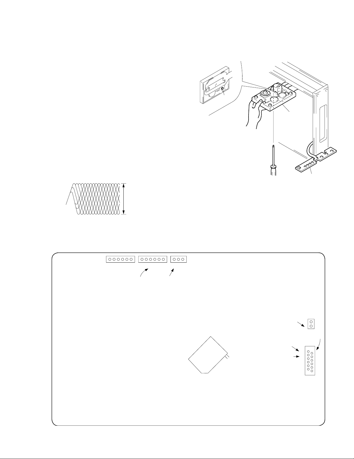
Skew Adjustment
(Be sure to perform this adjustment when the optical pick-up or a
mechanical part of the optical pick-up has been replaced.)
1. Remove the top plate. (See 3. Disassembly/Top Plate Assembly)
2. Remove the eight screw (+B3X8) of the top plate and remo ve the
KEY board.
3. Connect the KEY board connector and the DISPLAY board connector.
4. Remove the base unit. (Do not disconnect the connectors.)
(Refer to 3. Disassembly/Base Unit.)
5. Adjust with the unit placed sideways as shown in the figure.
6. Connect and oscilloscope to TP (RF: 1Pin of CN215).
7. While pressing the ±and ·buttons, press the POWER button. (The discrete open/close detection is turned OFF.)
8. Set a disk (YEDS-18) and press the ·button.
9. Rotate the adjustment screw with a Phillips screwdriver and adjust so that the oscilloscope waveform becomes clear.
Note: A clear RF signal waveform means that the shape “◊” can be
clearly distinguished at the center of the waveform.
RF signal waveform
VOLT/DIV : 200mV
TIME/DIV : 500ns
Adjustment
screw
Base unit
Note: Hold the base
unit horizontally.
KEY BOARD
level : 1.2 Vp-p
10.After the adjustment, lock the adjustment screw.
[ SERVO BOARD ] — Conductor Side —
CN514
6 4 1
(PLK)
+0.25
–0.20
CN513
(ADJ)
3 1
CN515
IC101
29 (FEI)
27 (TEI)
(VC)
(FE)
(RF)
CN215
1
CN210
12
10
2
(TE)
11
1
— 11 —
 Loading...