

Sony CDPEX-100 Service manual
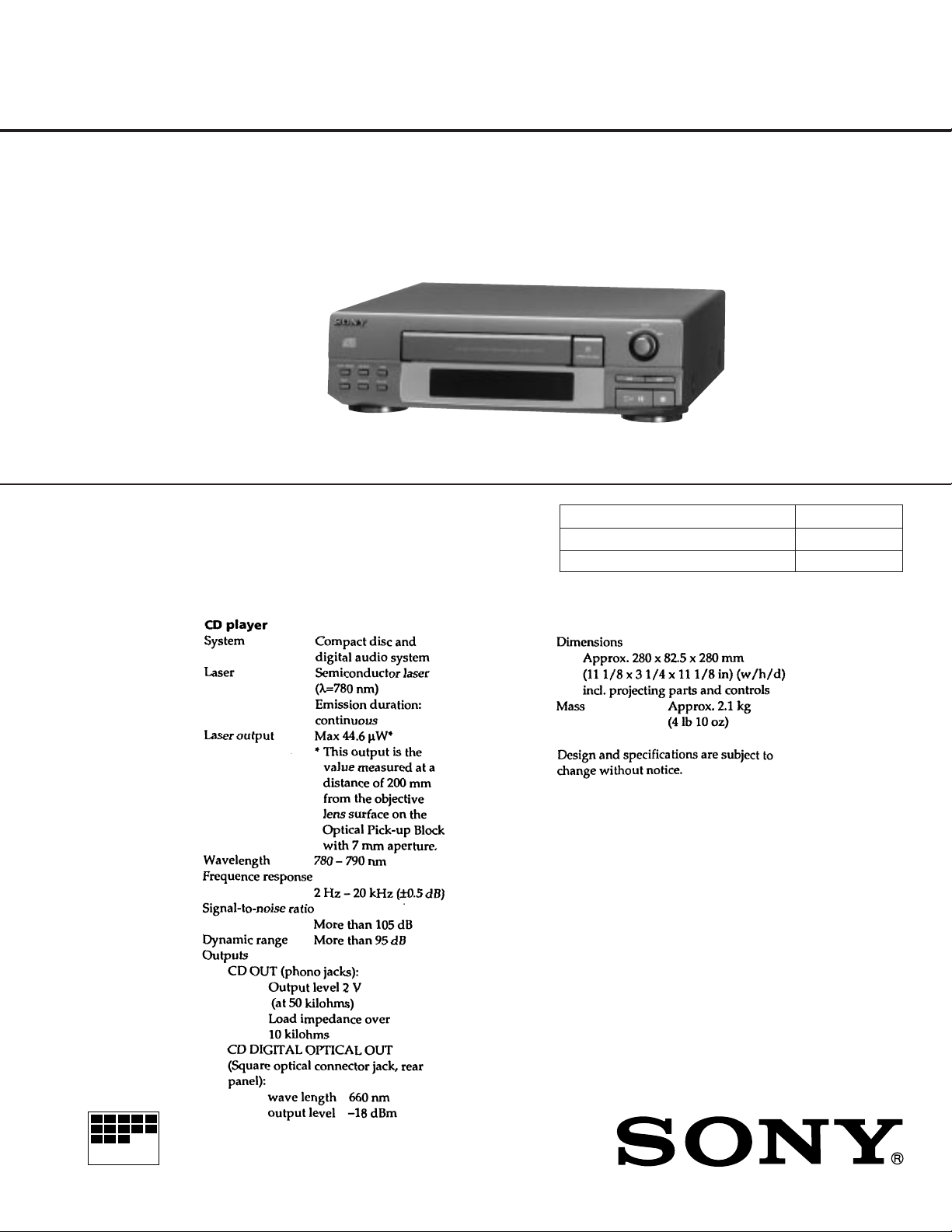
CDP-EX100
SERVICE MANUAL
This set is the CD player section in
MHC-EX50/EX70AV/EX100AV.
SPECIFICATIONS
AEP Model
UK Model
E Model
Model Name Using Similar Mechanism CDP-EX10
CD Mechanism Type CDM28-5BD19
Base Unit Name BU-5BD19
MICROFILM
COMPACT DISC PLAYER
– 1 –
The laser component in this product
is capable of emitting radiation
exceeding the limit for Class 1.
TABLE OF CONTENTS
1. SERVICE NOTE .................................................................. 3
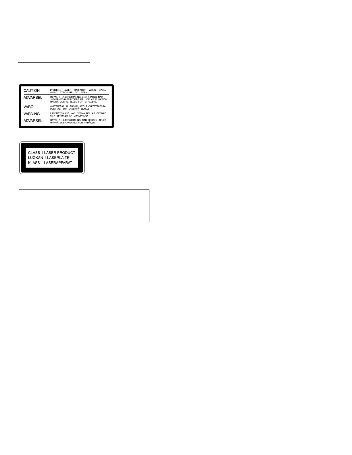
The following caution label is located inside of the unit.
This appliance is classified
as a CLASS 1 LASER
product.
The CLASS 1 LASER
PRODUCT MARKING is
located on the rear exterior.
CAUTION
Use of controls or adjustments or performance of procedures other than those specified herein may result in hazardous radiation exposure.
Notes on Chip Component Replacement
• Never reuse a disconnected chip component.
• Notice that the minus side of a tantalum capacitor may be dam-
aged by heat.
2. GENERAL ............................................................................. 4
3. DISASSEMBLY
3-1. Loading Panel.......................................................................... 4
3-2. MD Block................................................................................ 5
3-3. Holder (BU) Assy.................................................................... 5
4. ELECTRICAL ADJUSTMENTS .................................... 6
5. DIAGRAMS
5-1. IC Pin Function ....................................................................... 8
5-2. Circuit Boards Location ........................................................ 10
5-3. Printed Wiring Board – BD Section –................................... 11
5-4. Schematic Diagram – BD Section –...................................... 13
5-5. Printed Wiring Boards – Main Section – .............................. 16
5-6. Schematic Diagram – Main Section –................................... 19
6. EXPLODED VIEWS
6-1. Chassis Section...................................................................... 26
6-2. Front Panel Section ............................................................... 27
6-3. CD Mechanism Section......................................................... 28
6-4. Base Unit Section .................................................................. 29
7. ELECTRICAL PARTS LIST .......................................... 30
NOTES ON HANDLING THE OPTICAL PICK-UP BLOCK OR
BASE UNIT
The laser diode in the optical pick-up block may suffer electrostatic
breakdown because of the potential difference generated by the
charged electrostatic load, etc. on clothing and the human body.
During repair, pay attention to electrostatic breakdown and also use
the procedure in the printed matter which is included in the repair
parts.
The flexible board is easily damaged and should be handled with
care.
NOTES ON LASER DIODE EMISSION CHECK
The laser beam on this model is concentrated so as to be focused on
the disc reflective surface by the objectiv e lens in the optical pick-up
block. Therefore, when checking the laser diode emission, observe
from more than 30 cm away from the objective lens.
SAFETY-RELATED COMPONENT WARNING!!
COMPONENTS IDENTIFIED BY MARK ! OR DOTTED LINE
WITH MARK ! ON THE SCHEMATIC DIAGRAMS AND IN THE
P AR TS LIST ARE CRITICAL TO SAFE OPERATION. REPLACE
THESE COMPONENTS WITH SONY PARTS WHOSE PART
NUMBERS APPEAR AS SHOWN IN THIS MANUAL OR IN
SUPPLEMENTS PUBLISHED BY SONY.
– 2 –
SECTION 1
SERVICE NOTE
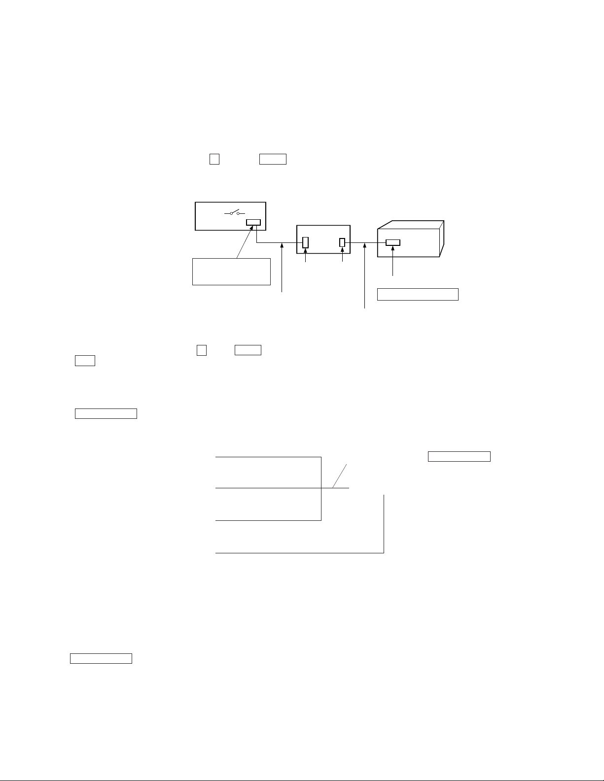
• How to operate with a single unit
Normally this set does not operate with a single unit.
When you must be mending, connect to other unit.
If the SYSTEM POWER switch of the amplifire is set to ON, the
power supply of the set is turned on.
In case of other unit is nothing, the service box (PFJ-1) and
exclusive jig (J-2501-078-A) are necessary to operate the set with
a single unit.
In case of above mentioned, press the p button and TIME button
at the same time, to enter the power on.
SERVICE BOX (PFJ-1)
POWER SW
JIG
(J-2501-078-A)
SET
FH-E939, 838, 737
CDP/TC
CORD WITH CONNECTOR 17P
(attached to PFJ-1)
• FL tube/ KEY check mode
After to enter the power on, when p button, TIME button and
) button are pressed at the same time, you will be check FL
tube.
Whenever press the above mentioned three buttons at the same
time, change to check mode of FL tube.
Under check mode of FL tube when any pressing button or turn
= AMS + button, change to KEY check mode.
To finish KEY check mode, press the above mentioned three
buttons at the same time.
All FL tube indicator light on
nn n
(Press three buttons at the same time)
A segment pattern mode 1
(Press three buttons at the same time)
A segment pattern mode 2
(Press three buttons at the same time)
Finish the test mode
9
CN904
17P
CN902
7P
CORD WITH CONNECTOR 7P
(attached to set)
CN301 7P
SYSTEM CONTROL
Any pressing button or turn = AMS + button.
(
(
KEY check mode
(Press three buttons at the same time)
Note 1)
All FL tube light on mode is kept when three buttons which is
pressed to enter all FL tube light on mode, release at the same time.
If you will be release failure them, it is moved to KEY check mode
after all FL tube light on mode.
Note 2)
Under KEY check mode, every time and button pressed or
= AMS + button turned on, figure on “ KEY= ” of FL tube
is increased.
– 3 –
SECTION 2
GENERAL
Front Panel Display Window
This section is extracted from
instruction manual.
SECTION 3
DISASSEMBLY
Note : Follo w the disassembly procedure in the numerical order giv en.
3-1. LOADING PANEL
bottom of chassis
1
Turn the cam in the
direction of arrow.
bottom of chassis
2
Pull out the disc table.
– 4 –
3
claws
4
Remove the loading panel
in the direction of arrow.
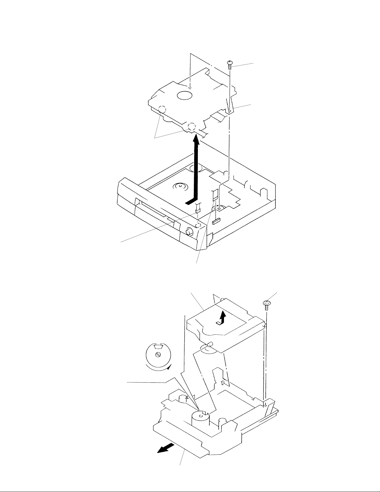
3-2. MD BLOCK
4
claws
3
BVTP 3×8
5
MD block
(CDM28-5BD19)
1
CN202
3-3. HOLDER (BU) ASSY
1
Turn the cam in the direction of arrow.
4
holder (BU) assy
(BU-5BD19)
2
CN201
3
yoke bracket
2
Pull out disc table.
– 5 –
SECTION 4
ELECTRICAL ADJUSTMENTS
Note :
1. Basically designed to operate without adjustment. Therefore, check
each item in order given.
2. Use YEDS-18 disc (3-702-101-01) unless otherwise indicated.
3. Use an oscilloscope with more than 10MΩ impedance.
4. Clean the objective lens by an applicator with neutral detergent
when the signal level is low than specif ied value with the following
checks.
5. Adjust the focus bias adjustment when optical block is replaced.
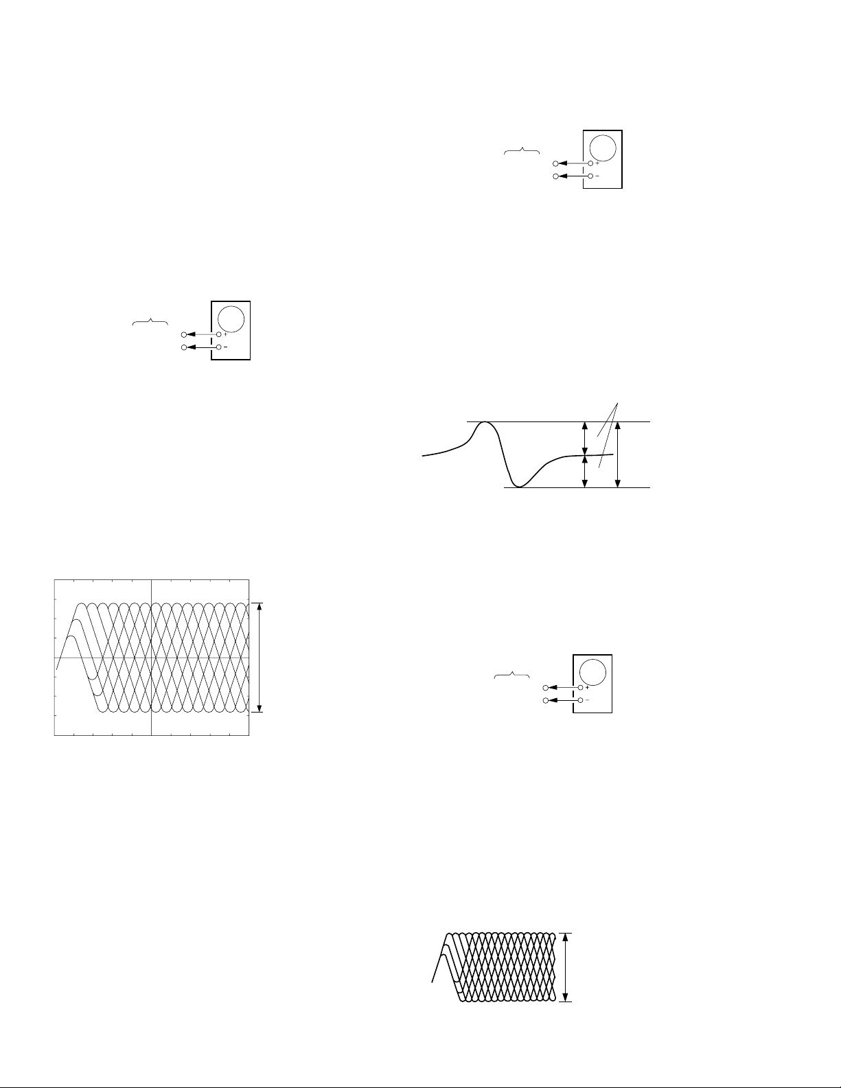
Focus Bias Adjustment
oscilloscope
(DC range)
BD board
TP (RF)
VC
Procedure:
1. Connect oscilloscope to test point TP (RF). (GND terminal : VC)
2. Turn Power switch on.
3. Put disc (YEDS-18) in and playback.
4. Adjust RV101 so that the waveform is clear.
(Clear RF signal waveform means that the shape “ ≈ ” can be
clearly distinguished at the center of the waveform.)
5. After adjustment, check the RF signal level.
S Curve Check
oscilloscope
BD board
TP (FEO)
TP (FOK)
Procedure:
1. Connect oscilloscope to test point TP(FEO).
2. Connect between test point TP(FOK)and GND by lead wire.
3. Turn Power switch on.
4. Put disc (YEDS-18) in and turnd Power switch on again and
actuate the focus search. (In case of using SER VICE BO X actuate
the focus search when disc table is moving in and out.)
5. Check the oscillosope waveform (S-curve) is symmetrical between
A and B. And conf irm peak to peak level within 2.4±0.7 Vp-p.
S-curve waveform
symmetry
A
within 2.4±0.7 Vp-p
B
• RF signal
VOLT/DIV : 200 mV
TIME/DIV : 500 nS
level
1.3±0.3 Vp-p
6. After check, remove the lead wire connected in step 2.
Note : • Try to measure several times to make sure than the ratio of
A:B or B:A is more than 10:7.
• Take sweep time as long as possible and light up the
brightness to obtain best waveform.
RF Level Check
oscilloscope
BD board
TP (RF)
TP (VC)
Procedure:
1. Connect oscilloscope to test point TP (RF) on BD board.
2. Turn Power switch on.
3. Put disc (YEDS-18) in and playback.
4. Confirm that oscilloscope waveform is clear and check RF signal
level is correct or not.
Note :
Clear RF signal waveform means that the shape “ ≈ ” can be clearly
distinguished at the center of the waveform.
RF signal waveform
VOLT/DIV : 200mV
TIME/DIV : 500nS
– 6 –
level : 1.3±0.3 Vp-p
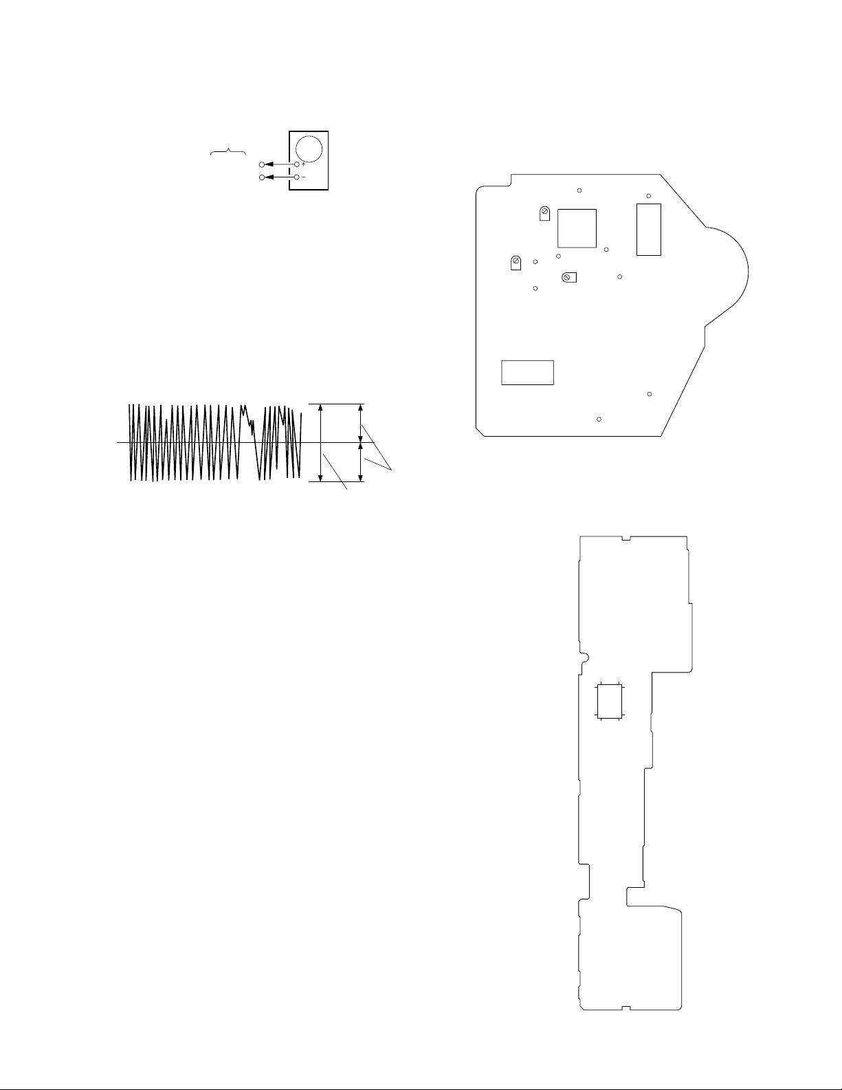
E-F Balance Check
oscilloscope
BD board
TP (TEO)
TP (VC)
Procedure:
1. Connect oscilloscpe to test point TP (TEO).
2. Turn Power switch on.
3. Connect pin @¢ of IC60I on the P ANEL board to GND with a lead
wire.
4. Put disc (YEDS-18) in and playback.
5. Push TIME button.
6. Confirm that the oscilloscope waveform is symmetrical on the top
and bottom in relation to 0Vdc, and check this level.
Adjustment Location :
[BD BOARD] (Conductor Side)
RF
RV101
IC101
RV103
TEO
VC
RV102
FEO
TEI
FEI
FOK
IC102
Traverse waveform
0V
symmetry
level : 300±100 mVp-p
7.Remove the lead wire connected in step 3.
Focus/Tracking Gain Adjustment (RV102, 103)
This gain has a margin, so even if it is slightly off.
There is no problem.
Therefore, do not perform this adjustment.
Please note that it should be fixed to mechanical center position when
you moved and do not know original position.
IC104
GND
PCK
[PANEL BOARD] (Conductor Side)
40
25
65
IC601
24
1
80
41
64
– 7 –
 Loading...