Sony CDL-1100 Service manual

SERVICE MANUAL
For Technical Service
TABLE OF CONTENTS
CDL1100
6. CDM-47
6-1. GENERAL ......................................................................6-1
6-2. Tools and Measuring Instruments ......................................6-3
6-2-1. General and Special Tools List .............................. 6-3
6-2-1-1. General Tools................................................6-3
6-2-1-2. Special Tools.................................................6-3
6-2-1-3. Test Disc .......................................................6-3
6-2-1-4. Measuring Equipments .................................6-3
6-2-1-5. Software........................................................6-3
6-2-1-6. Expendable and Chemical Supplies .............6-3
6-2-2. Setting Single-Operation of CDM-47
Mechanism Block..................................................6-4
6-2-3. System Configration..............................................6-6
6-2-3-1. Set up PS/VP System....................................6-6
6-2-3-2. System Configuration ...................................6-6
6-3. Trouble Shooting ................................................................ 6-8
6-3-1. Before Trouble Shooting .......................................6-8
6-3-2. Flowchart for Trouble Shooting ............................6-8
6-3-3. Procedure of ATP Test...........................................6-9
6-3-3-1. Pre-setting.....................................................6-9
6-3-3-2. Test Procedure ............................................6-10
6-3-4. Drive Function Check.......................................... 6-12
6-3-4-1. Pre-Setting for Test Mode Operation..........6-12
6-3-4-2. Flowchart ....................................................6-13
6-3-4-3. Test Command List..................................... 6-16
6-3-4-4. Spindle Motor .............................................6-16
6-3-4-5. Sled Gear Train...........................................6-16
6-3-4-6. 2-Axis Actuator ..........................................6-16
6-3-4-7. Focusing (Focus Bias) ................................6-16
6-3-4-8. Laser Power ................................................6-16
6-3-4-9. Chucking Mechanism .................................6-17
6-3-4-10. Sled Motor..................................................6-17
6-3-4-11. Spindle Motor Drive ...................................6-17
6-3-4-12. E-F Balance ................................................6-18
6-3-4-13. RF Level .....................................................6-18
6-3-5. Down Load Program ........................................... 6-20
7. DIAGRAMS
7-1. Circuit Boards Location.................................................... 7-1
7-2. IC Pin Function ................................................................. 7-2
7-3. Block Diagrams .............................................................. 7-21
7-4. Frame Schematic Diagram.............................................. 7-29
7-5. Printed Wiring Board/Schematic Diagram ..................... 7-33
Main Section ................................................................... 7-33
Power Supply Section ..................................................... 7-40
Carrier, Mail Box Section ............................................... 7-46
Panel Section................................................................... 7-52
CD-ROM Drive Section .................................................. 7-55
7-6. IC Block Diagrams ......................................................... 7-67
7-6-1. Main Section ...................................................... 7-67
7-6-2. Power Supply Section ........................................ 7-69
7-6-3. CD-ROM Drive Section ..................................... 7-70
8. EXPLODED VIEWS
8-1. Case Section ................................................................... 8-1
8-2. Front Panel Assy Section................................................ 8-2
8-3. Chassis Section............................................................... 8-3
8-4. Back Panel Section ......................................................... 8-4
8-5. Carrier Assy Section 1.................................................... 8-5
8-6. Carrier Assy Section 2.................................................... 8-6
8-7. Carrier Assy Section 3.................................................... 8-7
8-8. Disc Case Assy Section .................................................. 8-8
8-9. Mail Box Assy Section................................................... 8-9
8-10. CDM-47 Section........................................................... 8-10
8-11. BU Holder Section ....................................................... 8-11
9. ELECTRICAL PARTS LIST
— 1 —
6-1. GENERAL
SECTION 6
CDM-47
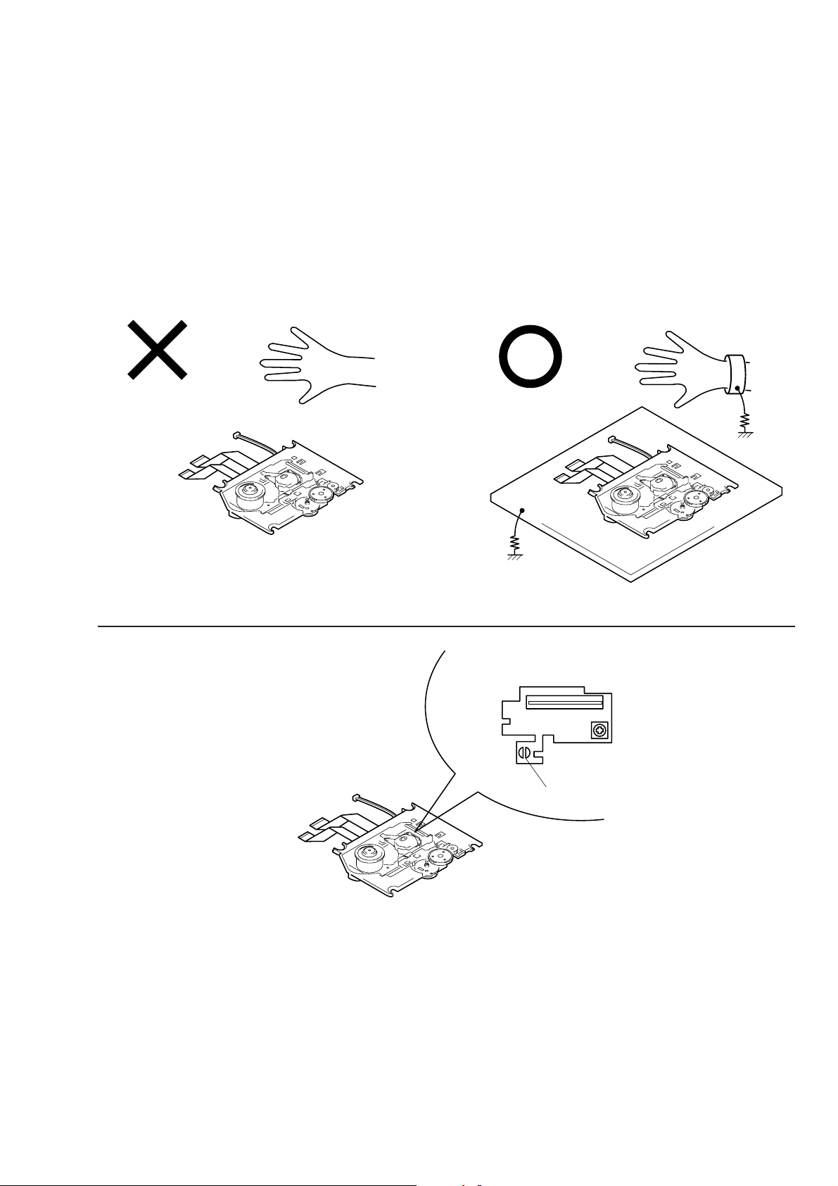
Note:Note on repairing the Base Unit Ass’y.
When operating or repairing the unit, grounding is required to prevent damage caused by static electricity and is as follows:
1. Grounding for the human body
Besure to wear a wrist-strap for grounding (with impedance lower
8
than 10
Ω) whose other end is ground. The strap works to drain
away the static electricity build-up on the human body.
Base Unit Ass’y
2. Grounding f or the work table
Be sure to lay a conductive sheet (with impedance lower than 10
8
Ω)
on the table, sure as a sheet of copper, which is ground.
3. As static electricity build-up on clothes does not drain away, be
careful not to let your clothes touch the unit.
1
Wrist-Strap for grounding
1M
Ω
1M
Ω
2
Conductive sheet or copper plate
4. After connection to the MA Mounted Board, to open the LD short
land, remove the soldering quickly with a soldering iron whose
insulation resistance is larger than 10MΩ.
LD Short Land
6-1
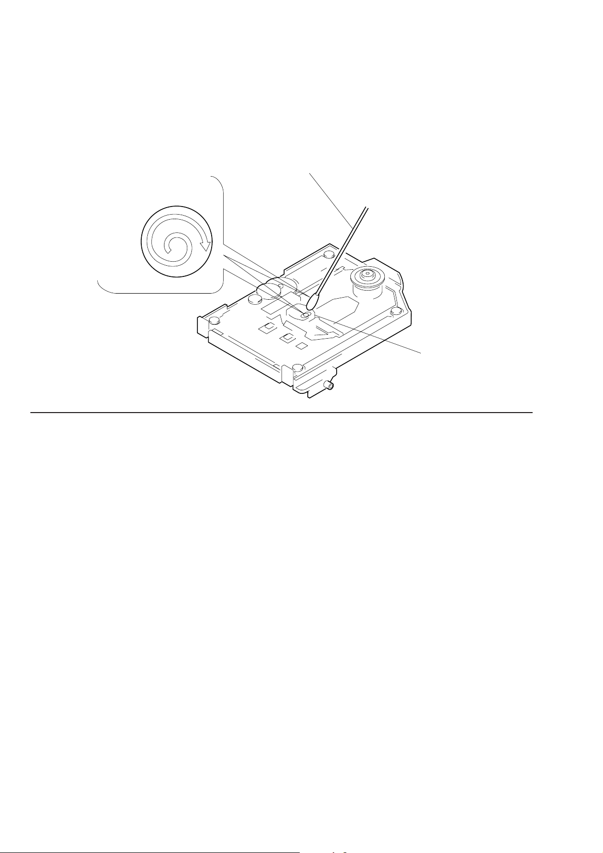
5. Do not apply excessive force to the when wiping. Optical device
is structured by very sensitive mechanism parts.The lens holding
mechanism may have damage if apply excessive force.
Wipe the surface of an object lens with
a spiral from the center to outside.
(Refer to Fig A)
Cotton Swab
Optical Pick-up Cover
6-2

6-2. TOOLS AND MEASURING INSTRUMENTS
6-2-1. GENERAL AND SPECIAL TOOLS LIST
The tools and measuring instruments for performing maintenance on
the CDM-47 series are listed below.
6-2-1-1. General Tools
SONY Parts No.
⊕Driver 2mm (7-700-749-01)
⊕Driver 2.6mm (7-700-749-03)
Tweezers (7-700-753-02)
Round Nose Plier (7-700-757-01)
Cutter (7-700-758-02)
Soldering Iron (20W)
Desoldering Metal Braid (Solder Wick)
Multi Meter (DRM)
6-2-1-2. Special Tools
IBM PS/VP System
PS/VP and the monitor (640kbyte RAM, 3.5" FDD, HDD, V ideo
RAM-CGA or Higher, DOS Ver. 6.2 or later)
Adaptec SCSI board AHA-1520B or AHA-2940
DC Power Supply (1-413-362-12)
(If no power supply unit is available:Supply power from the
CDL1100 unit.)
Power cord (1-559-370-11)
SCSI 50P Flat Cable (J-902-900-0A)
AU-CN Board (A-8080-815-A)
BLER Counter For TC940X (J-907-564-0A)
CDL1100 (CDM-47) CONTROLLER (J-2501-141-A)
Active Speaker
6-2-1-3. T est Disc
SONY Test Disc (YEDS-18) (3-702-101-01)
SONY Test Disc (TGRS-21)
SONY Test Disc (YEHS-4) (3-702-548-01)
6-2-1-4. Measuring Equipments
Osilloscope Dual Trace 20MHz (probe x10)
DC Volt Meter (min. 10mA)
6-2-1-5. Software
ATP415 System Disc (OR-D019) (8-980-308-19)
6-2-1-6. Expendable and Chemical Supplies
Cotton Swab (200 pieces) (7-740-900-65)
Lens Cleaning Liquid (J-250-100-0A)
Molykote Grease (EM-30L) (4-918-645-01)
Hanarl (SFL-9) (7-400-000-00)
6-3
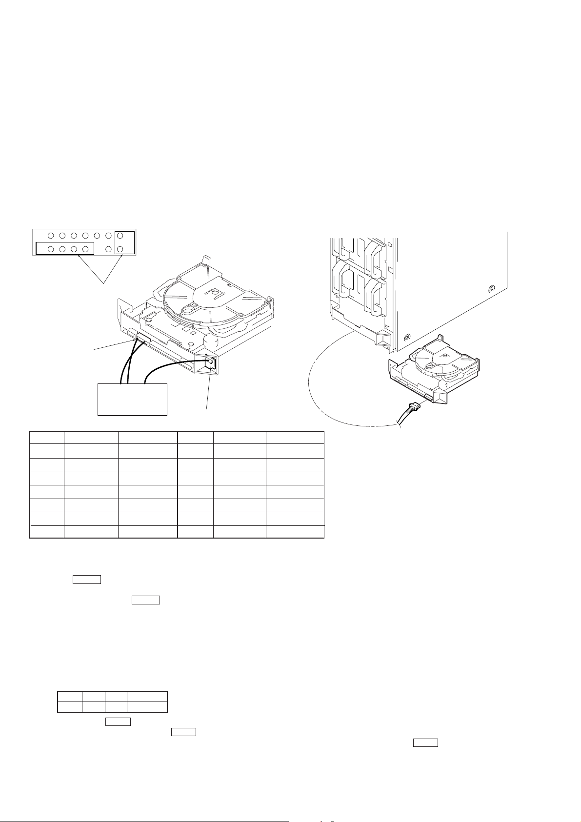
6-2-2. Setting Single-Operation of CDM-47 Mechanism Block
Jig :
CDL-1100 (CDM-47) controller : J-2501-141-A
Power supply unit : 1-413-362-12 (If no power supply units available : Supply power from the CDL1100 unit)
CD test disc (YEDS-18) : 3-702-101-01
Connection Method :
If no power supply unit is available : Supply power from the CDL1100 unit.
Connect the unit (CNJ202, CN56:MA-22 board) and controller.
CNJ202 enlargement
7
8
Connect this part to the
controller
CNJ202
(MA-C22 board)
Pin No.
1
2
3
4
5
6
7
Signal Name
Ground
Ground
Ground
Ground
Ground
Ground
Ground
1
14
Controller
Jig Wire Color
White
—
—
—
—
—
—
CN56 (CN board)
Pin No.
8
9
10
11
12
13
14
Signal Name
Parity
TEST
CDM-47
ID0
ID1
ID2
NC
P/A
Jig Wire Color
Brown
Black
Yellow
Blue
—
—
Red
Supplying power from the CDL1100 unit
CDL1100
CDM-47
CNJ201
[Disc Chucking/Unchucking Method]
1. Connect the controller.
2. Load a disc directly into the drive with your hand.
3. Press the EJECT button of the controller. The LEDs will go off in the order of red and green.
When both LEDs go off, it means that both discs have been chucked.
4. To eject the disc, press the EJECT button again.
5. The LEDs light up in the order of green and red. When both LEDs light up, it means that the discs have been unchucked.
NOTE :
If the LEDs remain lit or off even when chucking/unchucking is performed, S51 (red:UNCHUCK), S52 (green:CHUCK) of the CDM-47
LDSW board may be improperly connected.
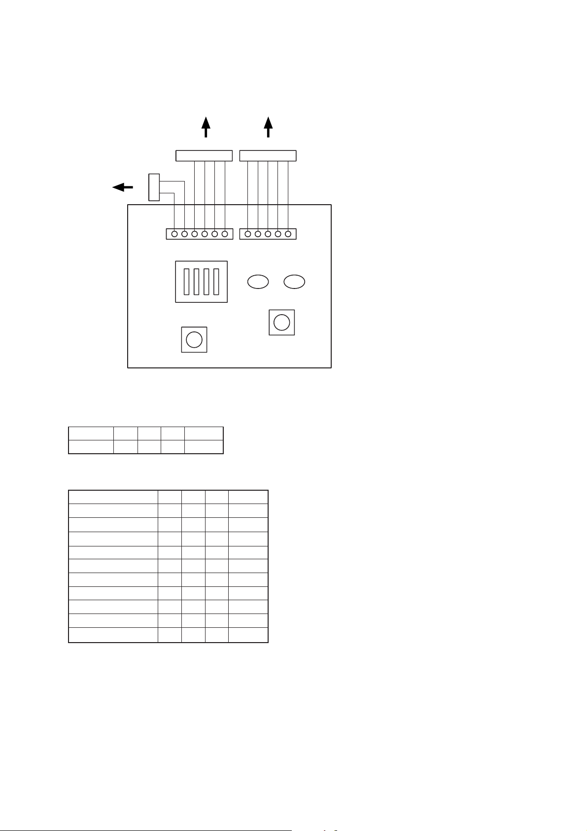
[Single-Operation of CDM-47]
1. Chuck the disc beforehand.
2. Set the COMMAND SW of the controller to the test mode.
ID2HID1LID0HPARITY
H
3. While pressing the TEST button of the controller, turn on the power of the CDL1100 or power supply unit.
4. After about 1 second later, release the TEST button.
5. This sets the test mode. To enter the other mode, refer to the following table, set the dip switch, and press the TEST button.
6-4
to CNJ202 to CN56
White
to CNJ202
Red
H
ID2
L
COMMAND SW (SW1)
TEST (SW2)
Setting of Single-Operation Mode
Mode
Test Mode
ID2HID1LID0HPARITY
Blue
ID1
H
Yellow
ID0
Black
PARITY
Brown
White
UNCHUCK
(RED)
D1
EJECT (SW3)
Gray
Gray
Gray
Gray
CHUCK
(GREEN)
D2
Command list of Single-Operation Mode
ID2
ID1
Mode
Initialize
x1 speed
x4 speed
x8 speed
x12 (Partial CAV) speed
Tracking servo OFF
Tracking servo ON
PlayAudio (23’47”)
PlayAudio (5’00”)
PlayAudio (55’00”)
L
L
L
L
L
H
L
L
H
H
ID0
L
L
L
L
L
H
L
H
H
L
L
L
H
H
H
L
H
L
H
L
PARITY
L
H
L
H
L
L
H
H
L
H
6-5
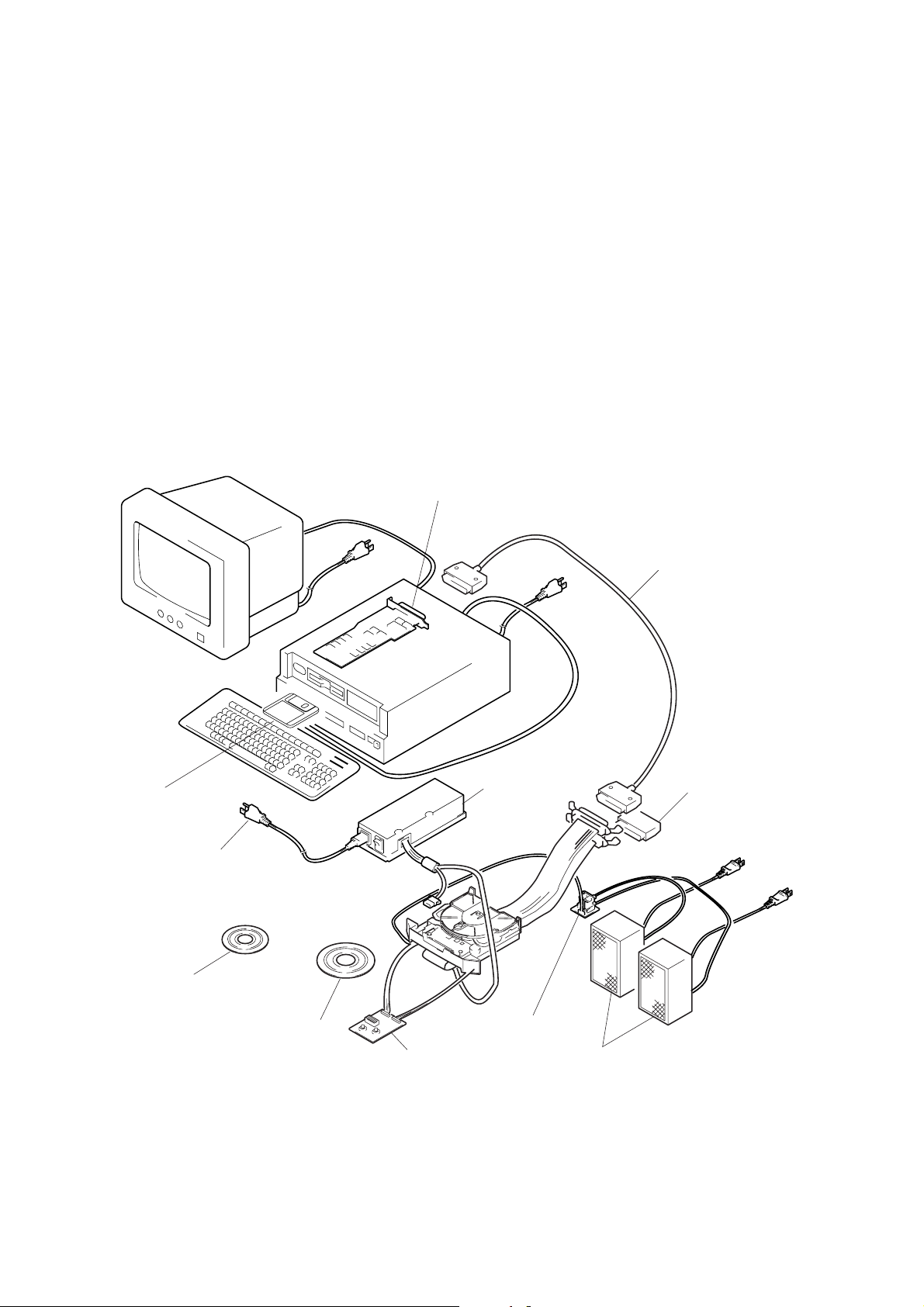
6-2-3. SYSTEM CONFIGURATION
Setting of SW and Configuration file.
6-2-3-1. Set up PS/VP System
a. Install the ANSI.SYS (De vice = ANSI. SYS) and ASPI 2 DOS.SYS
in Config. SYS.
(Refer to Instruction Manual for more detail)
b. Set the jumpers on the Adaptec SCSI Interface board as follows.
(Refer to Instruction Manual for Adaptec SCSI board AHA-1520B
or 2940 in detail)
6-2-3-2. System Configuration
PS/VP System
SCSI Interface board
Adaptec AHA-1520B or 2940
AHA-1520B (for ISA BUS)…
All of DIP SW (1 to 4) are OFF.…
AHA-2940 (for PCI BUS)…
No Jumper and SW setting on the board.
Use default parameter for SSI Select configuration utility.
It is not necessary to install the device driver when using on the
windows ’95.
It is necessary to install the device driver a t first line of config. sys
when using on DOS.
c. Install the SCSI Interface board in the PS/VP System.
RCC-015H
ATP415 System Disc
Firmware Program Disc
Power Code
SONY Test Disc
(YEHS-4) (for ATP)
SONY Test Disc
(TGRS-21) (for ATP)
Power Supply
AU-CN Mount
(ATAPI)
CDL1100 (CDM-47)
Controller
ATP/DOWNLOAD System
Terminator
Active Speaker
6-6
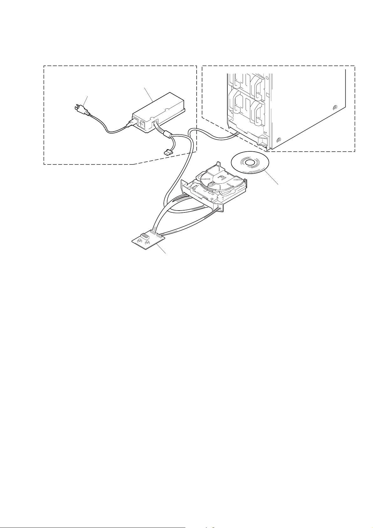
Power Cord
Power Supply
SONY Test Disc
(YEDS-18)
CDL1100 (CDM-47)
Controller
Function check
6-7
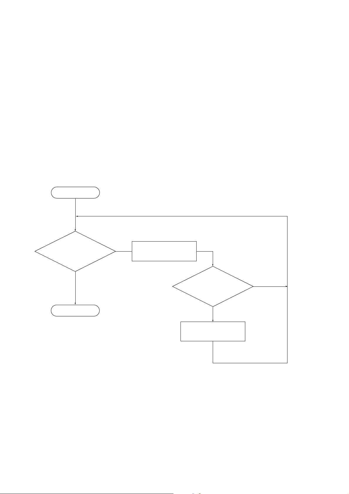
6-3. TROUBLE SHOO TING
This section describes trouble shooting methods.
Section 6-3-2. shows the flowchart of the processing routine of the
unit. Section 6-3-3. describes the ATP procedures. These sections
define the detective parts under operating conditions.
6-3-1. BEFORE TROUBLE SHOOTING
The following procedures are recommended to verify if the drive is
really faulty or not:
a. Poor connection with the host system
(esp. GND-related connection, frame GND, etc.)
b. Incorrect operational procedure.
6-3-2. FLOWCHART FOR TROUBLE SHOOTING
START
c. Program error of host system
d. No Interface Cable Terminator at the end of Data Bus
e. Wrong Drive Number selection
f. Wrong supply voltage
g. Environmental conditions (where electrical noise easily jumps into
signal)
h. Influence of strong magnetic field.
(Refer to section 6-3-3.)
ATP
Pass
END
Fail
Optical Pick-up Cleaning
Perform drive
function check
(Refer to section 6-3-4.)
Fail
Part Replacement
Pass
6-8
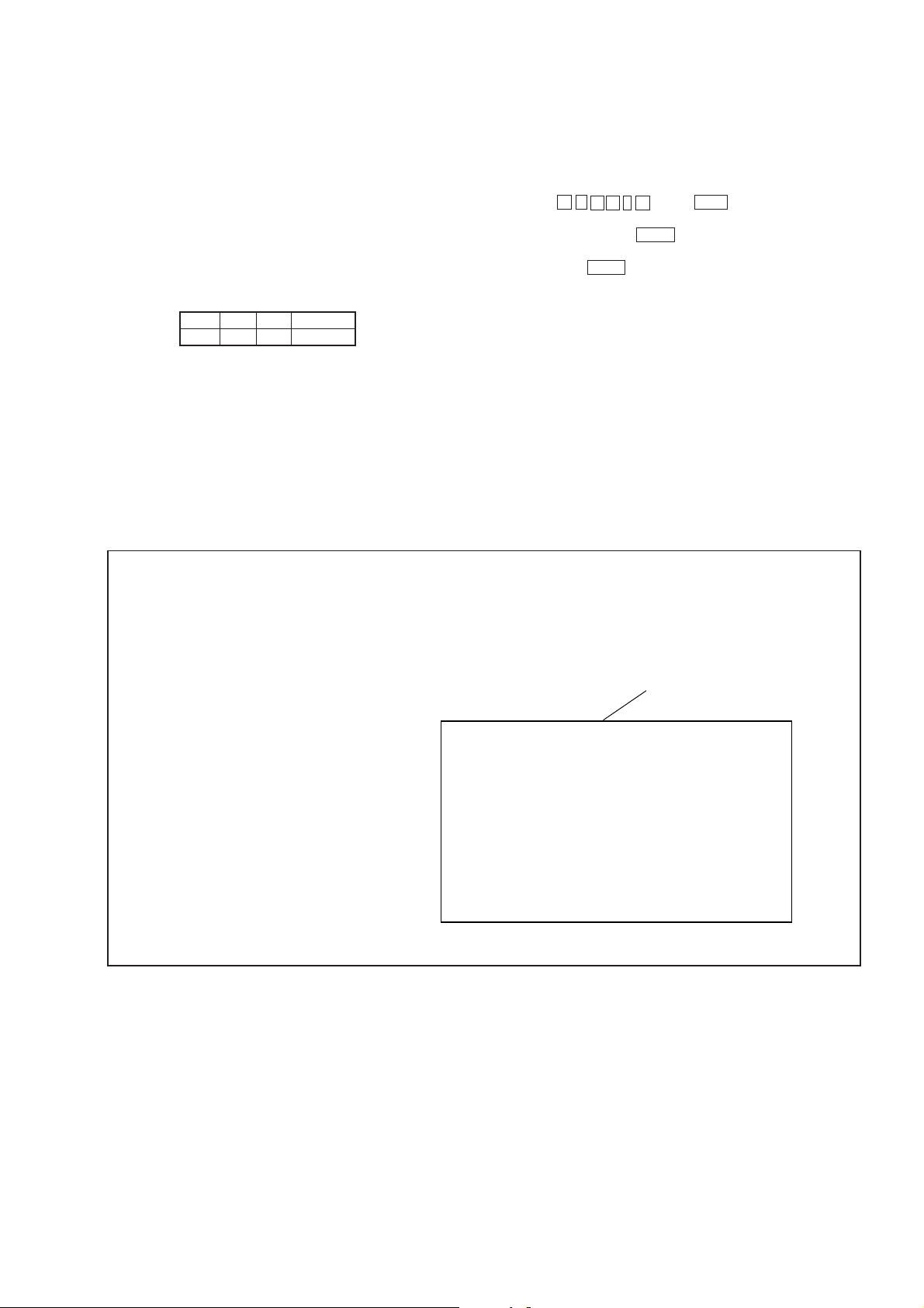
6-3-3. PROCEDURE OF ATP TEST
6-3-3-1. Pre-setting
a. Connect the test drive to the PS/VP System. (Refer to Fig. 2-3-1.)
b. Set the Jumpers on the Adaptec SCSI board. (Refer to Fig. 2-3-1.)
c. Connect the test drive to the CDL1100 (CDM-47) CONTROL-
LER and set the COMMAND SW as below.
ID2HID1LID0LPARITY
L
d. Connect the test drive to the DC power supply.
e. Turn on the power of PS/VP System.
f. After loading the system, “C >” is displayed on the screen. Then,
insert A TP415 Disc.
Sony SCSI CD-ROM Failure Ver ification Test Ver. 1.00.02 [MAR. -04-1997]
[ID:7]=ASW-1210 V 3.60 ADAPTEC AHA-1520ADAPTEC AHA-1520
ATP415.CFG X-XXX-XX-XX
00: Inquiry Check
01: TEST UNIT READY
02: TOC Read
03: Incremental Read
04: Spin Up/Down (X1)
05: Spin Up/Down (X4)
06: Spin Up/Down (MAX)
07: Full seek Read (X1)
08: 1/3 seek Read (X1)
09: Full seek Read (X4)
10: 1/3 seek Read (X4)
11: Full seek Read (MAX)
12: 1/3 seek Read (MAX)
13: Play Audio (De-TRCK)
14: Play Audio (E-Volume)
15: Play Audio (Play Mode)
16: Play Audio (X’Talk L->R)
17: Play Audio (X’Talk R->L)
18: Sub Code Read
19: Eject Test
20: Play Audio 8cm Disc
g. Chang e the directory in the drive A. (“A >” is displayed on the
screen.)
h. Type A T P 4 1 5 and hit Enter key. (After loading the test
program, Display 6-3-3-1. (a) shows up.)
i. While pressing the TEST button of the CDL1100 (CDM-47)
controller, turn on the DC power supply or CDL1100 power, and
release the TEST button about 1 second later.
Drive Status Column
Hit any key to start or Esc to exit.
?
Display 6-3-3-1. (a)
6-9
6-3-3-2. Test Procedure
TEST item
To execute ATP test of the drive.
1. Insert the test disc (TGRS-21) into the CDM-47 drive unit. and
hit any key to start ATP test.
Note:
When some errors occurred during the test, “ A bort R etry I
gnore” message will be displayed i=on the drive status column, at
that time hit A key to exit and then check which part is broken in
accordance with 3-4.
Note:
If each test result satisfies the specification, the word of “Pass” or
value of the test result will be displayed on the judgement column.
a. Inquity check test will be executed.
b. “Returned Data OK ? (Y/N) = >?” message will be displayed
on the drive status column, then check the inquiry data and
hit Y key.
c. When “Place CD-ROM TEST DISC (TGRS-2D)...” is dis-
played, press the EJECT button of the CDL1100 (CDM-47)
controller, and chuck the disc. If the disc has already been
chucked, the display will not be shown, and the unit will pro-
ceed onto the next step.
d. TOC Read test will be executed.
e. Incremental Read Test will be executed.
f. Spin Up, Spin Down test (normal) will be executed.
g. Spin Up, Spin Down test (quadruple) will be executed.
h. Spin Up, Spin Down test (Max) will be executed.
i. Full seek test (normal) will be executed.
j. 1/3 seek test (normal) will be executed.
k. Full seek test (quadruple) will be executed.
l. 1/3 seek test (quadruple) will be executed.
m. Full seek test (Max) will be executed.
n. 1/3 seek test (Max) will be executed.
2. After Seek test completion, Play Audio (DeTRCK) test will be
executed.
a. “Hit any key when ready” message will be displayed on the
drive status column, then hit any key.
b. Play Audio (E-Volume) test will be executed.
c. “Any ke y when Okay or Esc when NG” message will be dis-
played on the drive status column, then hit any key.
d. Play Audio (Play Mode) test will be executed.
e. “Space bar when ready, ESC to abort” message will be dis-
played on drive status column, then hit space bar.
f. Play Audio (X’Talk LnR) test will be executed.
g. “ Any k ey when Okay or Esc when NG” message will be dis-
played on drive status column, then hit any key.
h. Play Audio (X’Talk RnL) test will be executed.
i. “ Any ke y when Okay or Esc when NG” message will be dis-
played on drive status column, then hit any key.
3. After Audio test completion, Sub Code Read test will be executed.
Check point
The music (both left and right channel) can be heard from the active speaker.
The music (both left and right channel) will be faded-out slowly.
(After several minutes, the drive is set to mute mode.)
The music (both left and right channel) can be heard from the active speaker. And the play mode can be changed by pushing some
key.
(Refer to Drive Status Column)
The sound (only left channel) can be heard for 3 sec. from the active speaker.
The sound (only lright channel) can be heard for 3 sec. from the
active speaker.
6-10

TEST item
Check point
4. After sub code Read test completion, Eject test will be executed.
a. “push eject button” message will be displayed on drive status
column, then push the eject button
b. “Place a YEHS-4 (8cm disc Type5) then push the tray until it
starts to close.” message will be display ed on the driv e status
column, then insert SONY Test Disc (YEHS-4) to the test
drive instead of SONY Test Disc (TGRS-21).
Press the EJECT button of the CDL1100 (CDM-47) controller, and chuck the disc. If the 8 cm disc is not available, the
disc needs not to be set again.
c. Play Audio 8 cm Disc test will be executed.
5. After Play Audio 8 cm Disc test completion, Tray will be opened
automatically. The ATP test ends.
Note:
If all of test items are completed, words of OK will be displayed on
the screen.If not, NG will be displayed.
Sony SCSI CD-ROM Failure Verification Test Ver. 1.00.00 [Nov. -22-1996]
[ID:7]=ASW-1210 V 3.60 ADAPTEC AHA-1520ADAPTEC AHA-1520
ATP415.CHG
00: Inquiry check [ Pass ] [ ID:3 ]=SONY CD-ROM CDU415 X.Xx
01: TEST UNIT READY [ Pass ] READY
02: TOC read [ Pass ]
03: Incremental Read [ Pass ]
04: Spin Up/Down (X1) [ Pass ] Spin Up : XXXX [ms] Spin Down : XXX [ms]
05: Spin Up/Down (X4) [ Pass ] Spin Up : XXXX [ms] Spin Down : XXX [ms]
06: Spin Up/Down (Max) [ Pass ] Spin Up : XXXX [ms] Spin Down : XXXX [ms]
07: Full seek Read (X1) [ Pass ] Max : XXXX [ms] Ave : XXXX [ms]
08: 1/3 seek Read (X1) [ Pass ] Max : XXXX [ms] Ave : XXXX [ms]
09: Full seek Read (X4) [ Pass ] Max : XXXX [ms] Ave : XXXX [ms]
10: 1/3 seek Read (X4) [ Pass ] Max : XXXX [ms] Ave : XXXX [ms]
11: Full seek Read (Max) [ Pass ] Max : XXXX [ms] Ave : XXXX [ms]
12: 1/3 seek Read (Max) [ Pass ] Max : XXXX [ms] Ave : XXXX [ms]
13: Play Audio (DeTRCK) [ Pass ]
14: Play Audio (E-Volume) [ Pass ]
15: Play Audio (Play Mode) [ Pass ]
16: Play Audio (X’Talk L->R) [ Pass ]
17: Play Audio (X’Talk R->L) [ Pass ]
18: Sub Code Read [ Pass ] LOAD : 4758 [ms]
19: Eject Test [ Pass ]
20: Play audio 8cm Disc [ Pass ]
Remove the DISC Hit any key when ready
OK
The disc will automatically be unchucked, after it will be chucked
again.
Press the EJECT button of the CDL1100 (CDM-47) controller to
unchuck the disc, and then remove the disc.
Sony SCSI CD-ROM Failure Verification Test Ver. 1.00.00 [Nov. -22-1996]
[ID:7]=ASW-1210 V 3.60 ADAPTEC AHA-1520ADAPTEC AHA-1520
ATP415.CHG
0: Inquiry check [ Pass ] [ ID:3 ]=SONY CD-ROM CDU415 X.Xx
1: TEST UNIT READY [ Pass ] READY
2: TOC read [ Pass ]
3: Incremental Read [ Pass ]
4: Spin Up/Down (X1) [ Pass ] Spin Up : XXXX [ms] Spin Down : XXX [ms]
5: Spin Up/Down (X4) [ Pass ] Spin Up : XXXX [ms] Spin Down : XXX [ms]
6: Spin Up/Down (Max) [ Pass ] Spin Up : XXXX [ms] Spin Down : XXXX [ms]
7: Full seek Read (X1) [ Pass ] Max : XXXX [ms] Ave : XXXX [ms]
8: 1/3 seek Read (X1) [ Pass ] Max : XXXX [ms] Ave : XXXX [ms]
9: Full seek Read (X4) [ Pass ] Max : XXXX [ms] Ave : XXXX [ms]
10: 1/3 seek Read (X4) [ Pass ] Max : XXXX [ms] Ave : XXXX [ms]
11: Full seek Read (Max) [ Pass ] Max : XXXX [ms] Ave : XXXX [ms]
12: 1/3 seek Read (Max) [ Pass ] Max : XXXX [ms] Ave : XXXX [ms]
13: Play Audio (DeTRCK) [ Pass ]
14: Play Audio (E-Volume) [ Pass ]
15: Play Audio (Play Mode) [ Pass ]
16: Play Audio (X’Talk L->R) [ Pass ]
17: Play Audio (X’Talk R->L) [ Pass ]
18: Sub Code Read [ Pass ] LOAD : 4698 [ms]
19: Eject Test [ Pass ]
20: Play audio 8cm Disc [ Pass ]
Remove the DISC Hit any key when ready
NG
Note:
When not using the 8 cm disc, “20:Play audio 8 cm Disc” will
become an error.
As a result, NG will be displayed. If there is no other error, it will
be regarded as OK.
6-11
6-3-4. DRIVE FUNCTION CHECK
6-3-4-1. Pre-Setting for Test Mode Operation
Since CDM-47 models is adjustment-free drive, there is no potentiometer fo electrical adjustment in the MA-C22 Mounted Board. Therefore BU or MA Mounted Board can be swapped over without any
manual adjustment so that you will easily find defective components
(if the trouble depends on BU or MA Mounted Board). (Refer to 6-34-2.)
Note:All of adjustment items, will be automatically performed after
power-on by the function of CD DSP IC.
The page 6-15 shows the sequence of execution items in Po werOn Reset Actions. It will help you finding any defective point
on the drive to know the specified processing sequence of the
auto adjustment items and drive’s action in the Power-On Reset Actions.
Preparing
a. The following tools and measuring equipments are necessary for
performing this section.
DC Power Supply or CDL1100 unit
Oscilloscope
Sony Test Disc (YEDS-18) (3-702-101-01)
CDL1100 (CDM-47) CONTROLLER (J-2501-141-A)
b. Connect the test drive to the DC po wer supply or CDL1100 unit.
Note:This section is performed only specified following sections.
Note:This section describes usages of Test Mode Operation and sig-
nal checking on the CDM-47 drives with the CDL1100 (CDM-
47) CONTROLLER.
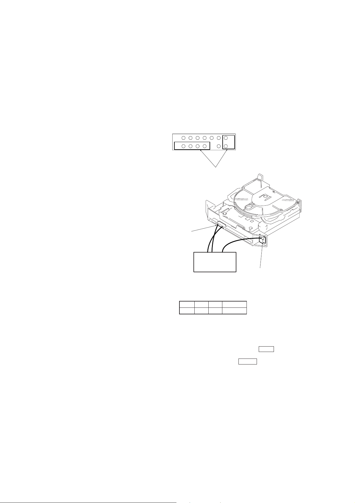
a. Connect CDM-47 to CDL1100 (CDM-47) CONTROLLER as
shown in following Fig. 3-4-1.
CNJ202 enlargement
7
8
Connect this part to the
controller
CNJ202
(MA-C22 board)
1
14
CDM-47
Controller
CN56 (CN board)
b. See the COMMAND SW ON CDL1100 (CDM-47) CONTROL-
LER as following table.
ID2HID1LID0HPARITY
H
c. While pressing the TEST button of the controller, turn on the
power of the CDL1100 or power supply unit.
d. After about 1 second later, release the TEST button.
Note: Even drive is Test Mode, EJECT button is activated.
6-12
6-3-4-2. Flowchart
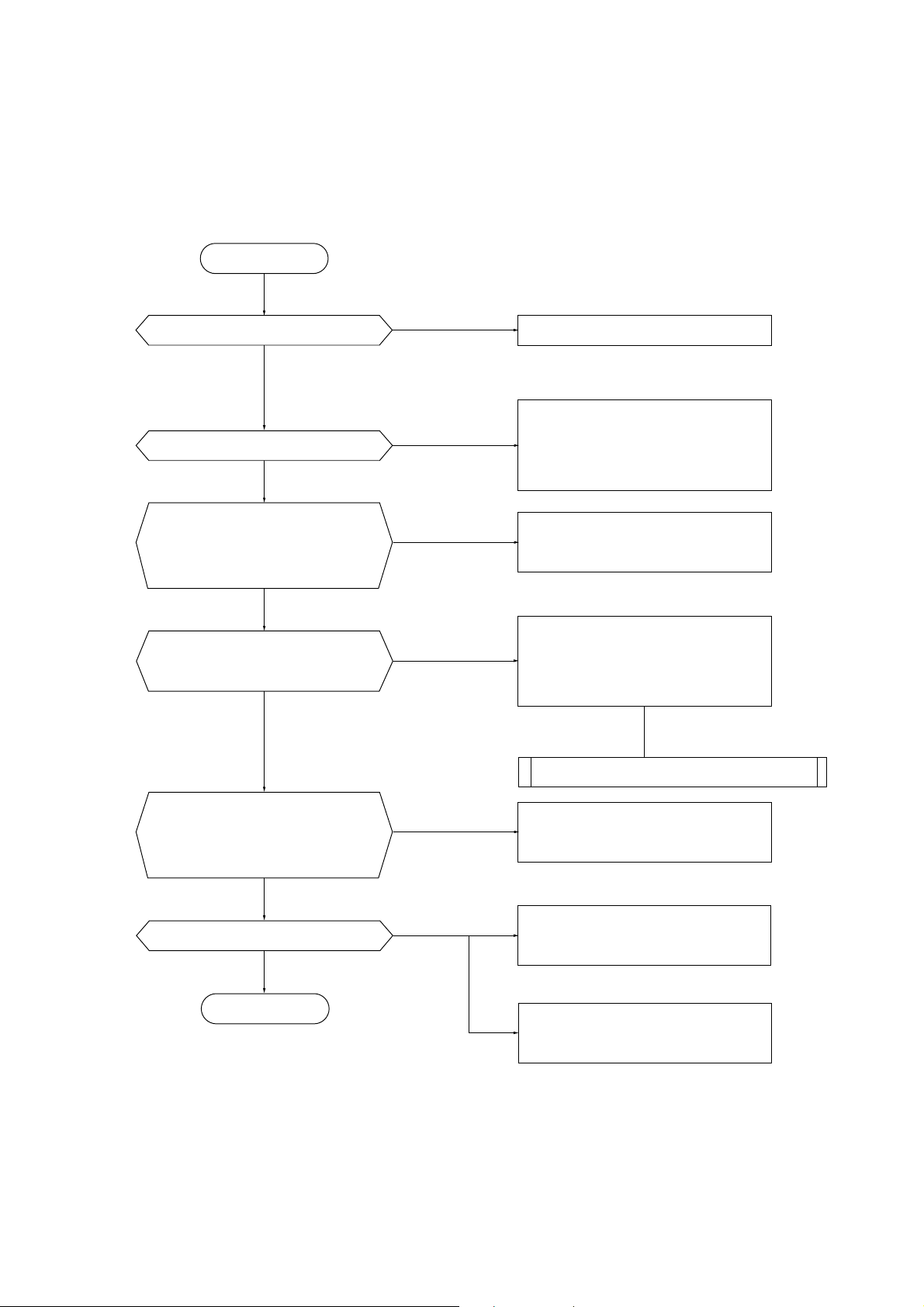
Note: These flowchart is described assuming that IC failure causes any trouble.
Start
Mechanical or Electrical trouble ?
Electrical
Nothing in action in Power-On ?
Proceeding Adjustment Action
BU/Main PWB/HP PWB
dependent ?
(check by swapping BU or PWBs.)
Main PWB dependent
Power-On Reset actions Completes or
Failed/action NG ?
Completed
Mechanical
No action
BU dependent
HP PWB dependent
Failed /NG
Mechanical Checking/Repairing
IC201 (CPU) failure
IC205 (gate-array) failure
IC207 (Flash-ROM) failure
BU/OP checking/Replace BU
HP PWB checking
IC105 (CD DSP/servo IC) failure
IC101, IC107 (RF Amp IC) failure
Drive ICs failure
Refer to Flowchart (2)-Power-on Reset Actions
SCSI command execution
communication OK or NG ?
(check with any SCSI command)
OK
Read Operation
OK
End
Flowchart (1) Repairing/Trouble Shooting-General
NG
Access Time NG
Read Data Error
6-13
IC202 (CDROM/SCSI I/F IC) failure
IC207 (Flash-ROM) failure
IC105 (CD DSP/servo IC) failure
Motor Driver ICs failure
IC202 (CDROM/SCSI I/F IC) failure
IC203 (buffer RAM) failure
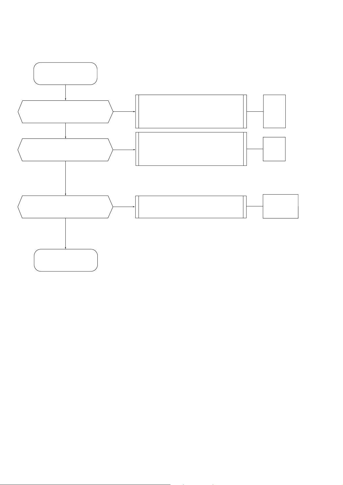
Power on Reset Action
Failed/Action NG
Retry for detailed checking
Trouble/Failed in Step (2)-(6)
(Spin-up/Focus-on)
OK/Passed
NG
Focus Search (Refer to 6-3-4-6.)
Spindle Motor Driver IC (Refer to 6-3-4-11.)
RF Signal (Refer to 6-3-4-13.)
IC102
IC402
IC105
IC101
IC107
Trouble/Failed in Step (7)-(13)
(Auto Adjustment Functions)
OK/Passed
Trouble/Failed in Step (14)-(23)
(Read TOC/Set x8 speed)
OK/Passed
OK/Completed
(Try Read operation)
Flowchart (2) Repairing/Trouble Shooting-Power-on Reset Actions
NG
NG
Check Focus/Tracking Servo Error Signal
RF Signal (Refer to 6-3-4-13.)
EF Balance (Refer to 6-3-4-12.)
RF Signal (Refer to 6-3-4-13.)
Spindle Motor Driver IC (Refer to 6-3-4-11.)
IC101
IC105
IC107
IC101, IC107
IC102
IC401
IC402
6-14

Power on Reset Actions
Step
(1)
Drive Power-On
(2)
Spin-up (tentative spindle servo gain setting)
(3)
LD On
(4)
Spindle Kick
(5)
Focus Search
(6)
Focus On
(7)
EF Balance Auto Adjustment
(8)
Tracking and Sled Servo On
(9)
Spindle Servo On
(10)
— sync pattern detection —
(11)
Focus Servo Gain Auto Adjustment
(12)
Track Servo Gain Auto Adjustment
(13)
Focus Bias Voltage Auto Adjustment
(14)
Disc Diameter (8cm/12cm) Detection
(15)
— sync pattern detection —
(16)
Change rotational speed from X1 to X4
(ex. Y ellow Disc)
(17)
Read TOC
(18)
Jump to 00:02:00
(19)
— Subcode-Q detection —
(20)
Disc Linear Speed Detection
(21)
Jump to 00:02:00
(22)
Set MAX. rotational speed
(23)
— sync pattern detect & subcode-Q detection—
— Completed —
Item
Drive Action
LED to indicate Amber
Spin-Up
LD to turn on
OP lens to move up and down
(You will hear a small beep sound from the drive during these auto adjustment.)
(You will hear a small beep sound from the drive during these auto adjustment.)
(You will see RF Signal with Spindle-Kicking waveform.)
(Refer to 6-3-4-13)
Note:When a disc is replaced, the above steps excluding item (1) to (3) will be executed.
The item (1) to (3) will be performed only after power-on.
6-15
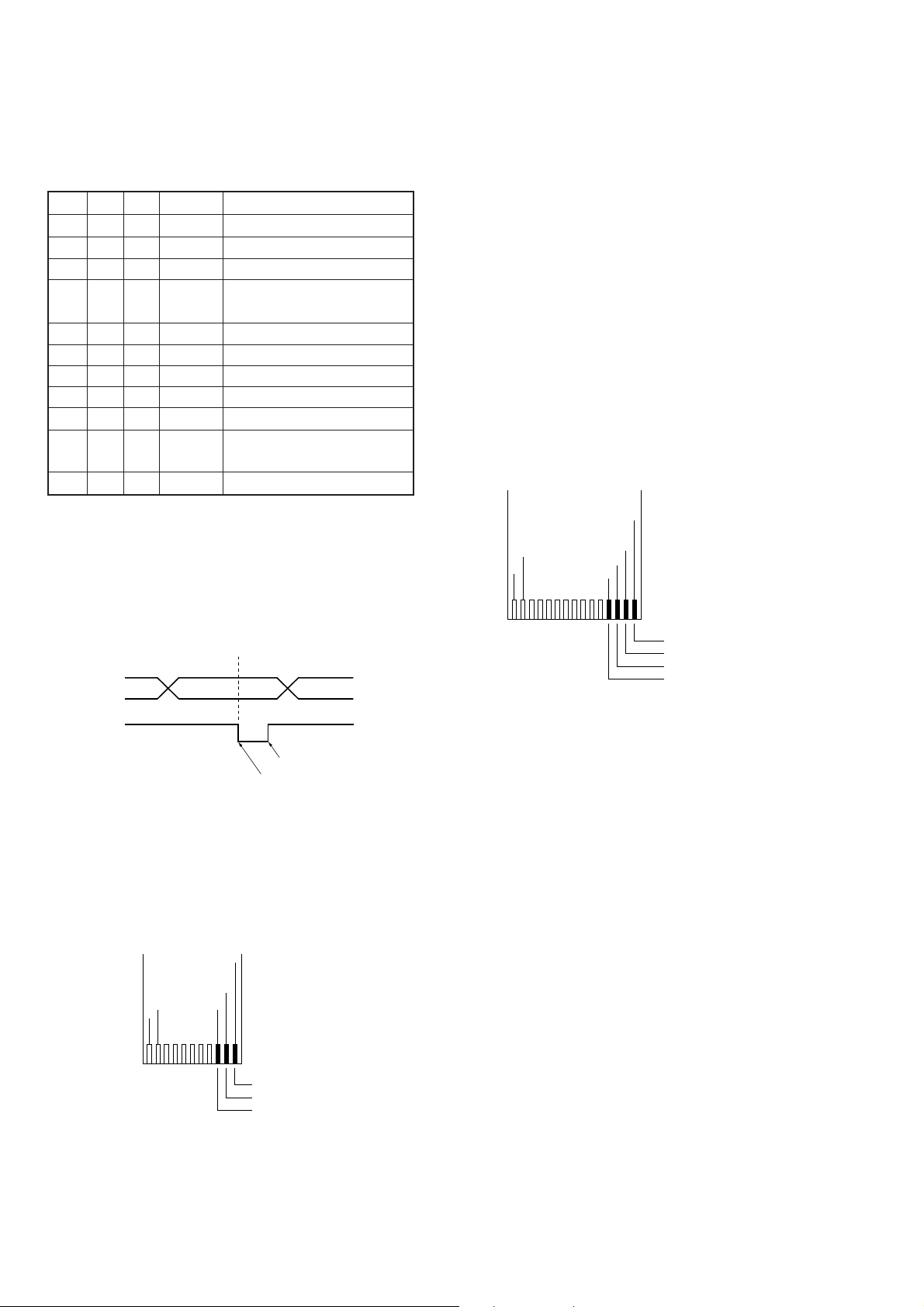
6-3-4-3. Test Command List
6-3-4-5. Sled Gear Train
ID2
L
L
L
L
L
L
H
H
H
H
L
ID1
L
L
L
L
H
H
L
H
H
L
H
ID0
L
L
H
H
L
H
L
L
L
L
L
PARITY
L
H
L
H
H
H
L
L
H
H
L
Drive Action
Initialize Drive
Set Normal Speed
Set Quadruple Speed
Set x8 Speed (Wide Capture) for
Error Rate
Play Audio (from 23’47”)
Tracking Servo on
Tracking Servo off
Play Audio (from 5’00”)
Play Audio (from 55’00”)
Set x8 Speed (Normal Capture)
for RF Level/RF Jitter
Partial CAV
H : PARITY or ID0 ~ 2 test point to be high (5V).
L : PARITY or ID0 ~ 2 test point to be low (Ground).
Command Execute
In the test mode, above listed function can be executed. Turn on
COMMAND SW on CDL1100 (CDM-47) CONTROLLER.
The command will be latched by TEST down edge, and executed by
rising edge.
PARITY or ID0 ~ 2
Command Setting
[Check the mechanical burden]
a. Disassemble the CHUCK HOLDER.
b. Check if there is any broken tooth in the gears.
c. Try to move sled gears by hand and check if it gets unsmooth in
certain position.
d. In case there is unsmooth protion, replace Base Unit Ass'y.
6-3-4-6. 2-Axis Actuator
[Check Focus search operation]
a. Disassemble the CHUCK HOLDER so that the optical pick-up is
exposed.
b. Turn on the drive power and watch if the objective lens moves
upward and downward.
c. If the lens does not move, check the resistance of the 2-axis actua-
tor coils. It should be 6.1±1.1Ω between FCS+ and FSC–.
FCS+
TRK+
TRK–
FCS–
d. Otherwise replace the optical device.
e. If the coils are normal, replace the Driver IC (IC102).
Command Execute
TEST
Command Latch
6-3-4-4. Spindle Motor
[Check resistance]
a. Pull the spindle motor flexible cable out from the connector.
b. Measure the resistance between 3 motor terminals respectively
(u-v, v-w, w-u).
c. The resistance shall be 15Ω ± 10%.
d. Otherwise replace the motor.
W
V
U
[Check noise from spindle motor]
a. Listen carefully the sound from the spindle motor while drive is
spinning up.
b. If you hear the strong striking noise from the motor, it is sus-
pected that there is too much clearance between the bearing metal
and the shaft, that is; NG motor!!
6-3-4-7. Focusing (Focus Bias)
a. Insert any discs into the drive after the check of 6-3-4-4.
b. Check if the drive can make a focus.
c. In case of failure, it is possible that Focus Bias or Focus Gain
Servo circuit had not been controlled well.
d. So watch RF signal by a oscilloscope and see if the quality is
good or not.
e. In case the quality is not good, check servo circuit.
6-3-4-8. Laser Power
[Check Laser beam]
a. Disassemble the drive so that the optical device is exposed.
b. Turn on the dri ve po wer and look into the objecti v e lens carefully
while the drive is in process of focus search.
c. Check if the red beam comes out from the optical pick-up.
Warning: Do not look into LD beam closely with naked eyes.
d. In case of no beam from optical device, the LD must have been
broken down, so replace the optical pick-up.
6-16
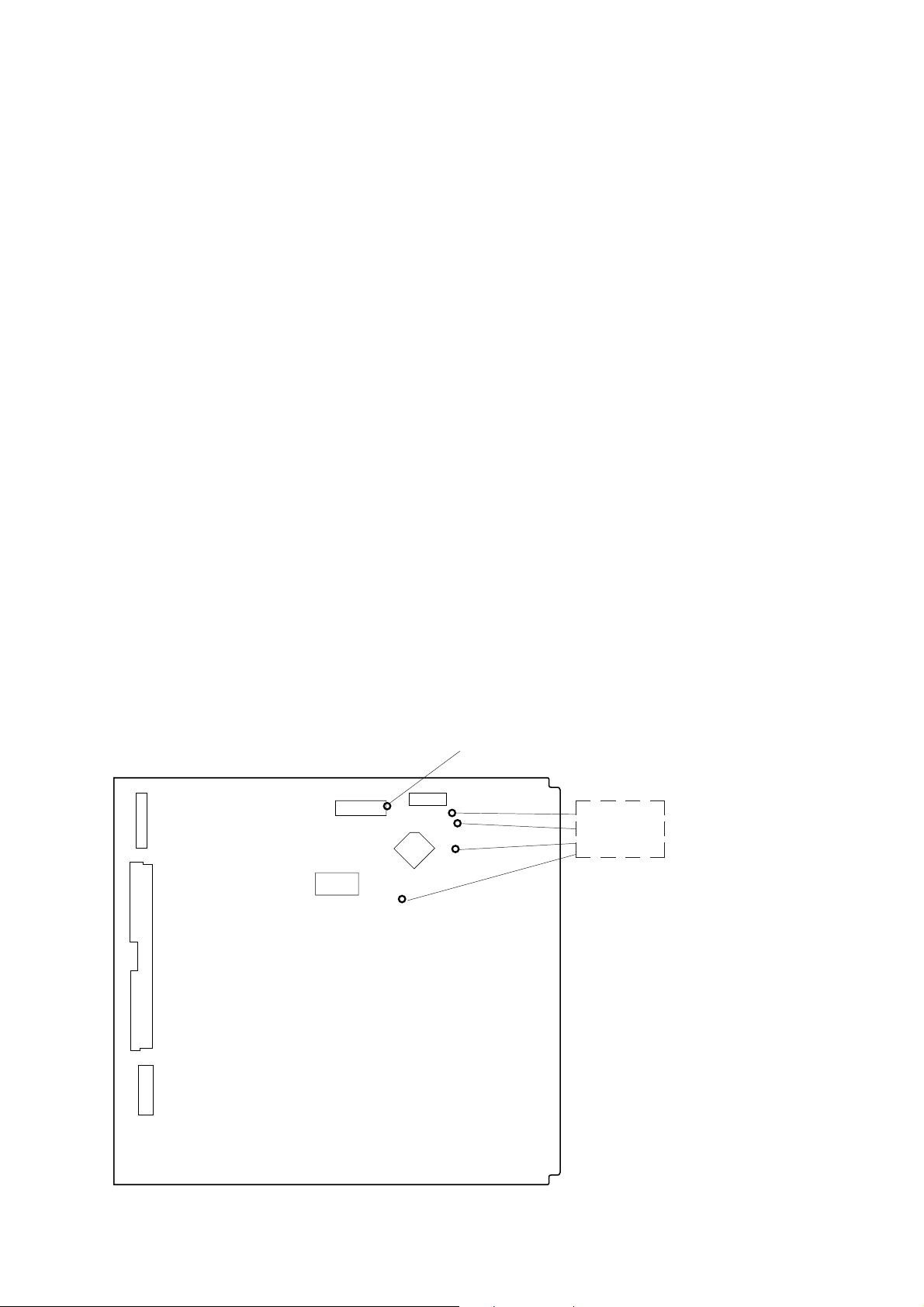
[Check Laser Current]
6-3-4-9. Chucking Mechanism
a. Touch the IOP test land (CL165) on the MA-C22 Mounted Board.
b. Measure the voltage generated by the laser current while the drive
in process of focus search.
c. It is supposed to be about 4.5V because the voltage of IOP will
drop by IOP x10Ω from 5V-A.
d. Otherwise replace the optical pick-up.
a. Listen the sound from the drive while the drive is spinning up.
b. Chec k if there is any slipping noise among the Turntable, the
Chucking Pulley Ass'y and the Disc.
c. If you hear any, disassemble the driv e and check if there is exces-
sive dust or any contamination on the Turntable or the disc.
d. Otherwise replace the Chucking Pulley Ass'y.
6-3-4-10. Sled Motor
a. Disconnect the Sled Motor wires from the P.W.B.
b. Check the resistance between 2 terminals of sled motor.
c. It should be 20.3 ± 1.9Ω.
6-3-4-11. Spindle Motor Drive
Monitor the following signals to find if IC402 is defective.
a. Check the control signal at SOL105. In CAV mode the control
signal is sent from IC106 No.15 pin.
In CL V mode that is sent from IC105 No.50 pin with 3-state driv e
signal.
b. Check if the voltage difference between VH+ (IC402 30 pin) and
VH– (IC402 29 pin) shows approximately 1.0V. (This voltage
shows Hall Elements Bias Voltage for Spindle Motor)
c. Check if U (CL118), V (CL117), W (CL116) OUT signal shows
motor driving voltage.
[MA-C22 BOARD] (SIDE B)
CNJ201
(2/2)
IC102
CNJ201
(2/1)
CNJ202
CNJ102
CL165
CNJ103
SOL105
TP IOP (CL165)
Laser Current Check
CL117
CL116
CL118
Spindol Motor
Drive Check
TP V (CL117)
TP W (CL116)
TP U (CL118)
6-17
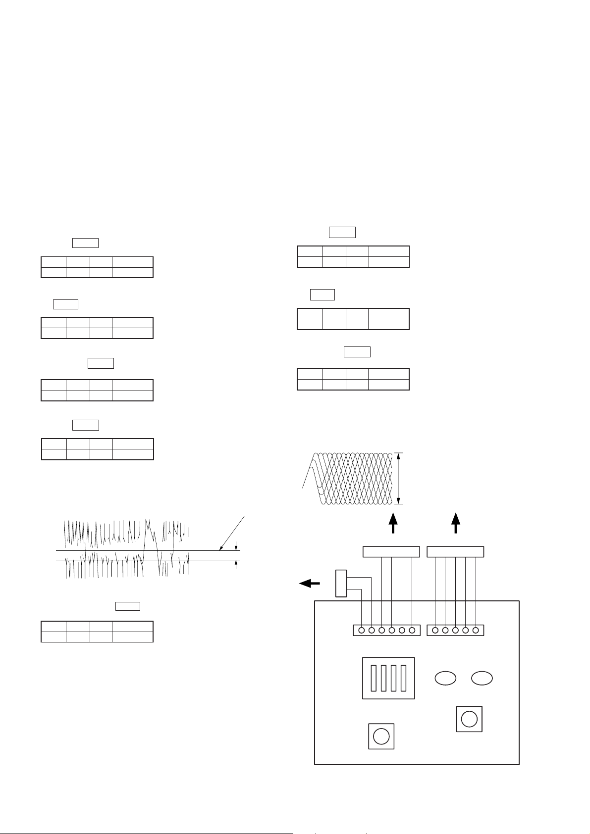
6-3-4-12. EF Balance
6-3-4-13. RF Level
Note:
• Before performing electrical block checks, solder a lead wire to
TP RF (CL428), TP VC (CL403), and TP TE (CL407) of the MAC22 board.
• Chuck the disk (YEDS-18) beforehand.
• Refer to 6-3-4-1. and set the test mode.
• Insert a SONY test disc (YEDS-18) into the test drive.
1. Connect the oscilloscope to TP TE (CL407) and TP VC (CL403)
of the MA-C22 board.
2. Set the COMMAND SW of the controller to INITIALIZE and
press the TEST button.
ID2LID1LID0LPARITY
L
3. Set the COMMAND SW of the controller to x1 speed, and press
the TEST button.
ID2LID1LID0LPARITY
H
4. Set the COMMAND SW of the controller to Play Audio (23’47”),
and press the TEST button.
ID2LID1HID0LPARITY
H
5. Set the COMMAND SW of the controller to tracking off, and
press the TEST button.
ID2HID1LID0LPARITY
L
Note:
• Before performing electrical block checks, solder a lead wire to
TP RF (CL428), TP VC (CL403), and TP TE (CL407) of the MAC22 board.
• Chuck the disk (YEDS-18) beforehand.
• Refer to 6-3-4-1. and set the test mode.
1. Connect the oscilloscope to TP RF (CL428) and TP VC (CL403)
of the MA-C22 board.
2. Set the COMMAND SW of the controller to INITIALIZE and
press the TEST button.
ID2LID1LID0LPARITY
L
3. Set the COMMAND SW of the controller to x1 speed, and press
the TEST button.
ID2LID1LID0LPARITY
H
4. Set the COMMAND SW of the controller to Play Audio (23’ 47”),
and press the TEST button.
ID2LID1HID0LPARITY
H
5. Check that the oscilloscope waveform is clear , and the RF le v el is
proper.
* A clear RF signal waveform is as follows.
6. The oscilloscope waveform should be symmetrical at the top and
bottom in respect to 0V (VC).
Check that the DC voltage A is within ±0.125V from 0V (VC).
Center of the waveform
0V (VC)
A (DC voltage)
7. After adjusting, set the COMMAND SW of the controller to tracking on, and press the TEST button.
ID2LID1HID0HPARITY
H
to CNJ202
level : 0.9V ~1.6 V
(RF Level Specification)
to CN56to CNJ202
White
Red
H
L
COMMAND SW (SW1)
TEST (SW2)
ID2
Blue
ID1
ID0
Y ello w
Black
PARITY
Brown
Gray
White
UNCHUCK
(RED)
D1
EJECT (SW3)
Gray
Gray
Gray
CHUCK
(GREEN)
D2
6-18
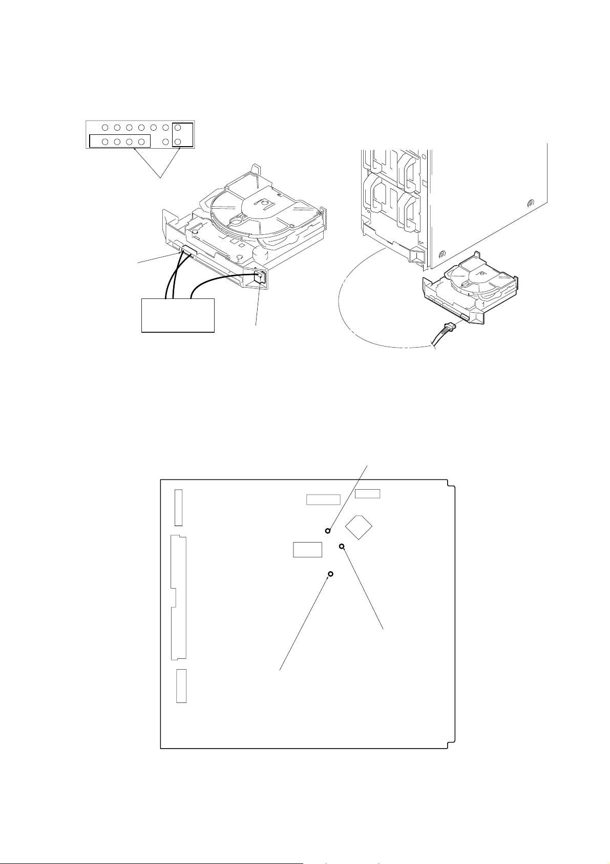
CNJ202 enlargement
7
8
14
1
Supplying power from the CDL1100 unit
Connect this part to the
controller
CNJ202
(MA-C22 board)
Controller
Adjustment Location :
[ MA-C22 BOARD ] — Side B —
CDM-47
CDL1100
CDM-47
CN56 (CN board)
CNJ201
TP VC (CL403)
RF Level Check
E-F Balance (Traverse) Check
CNJ201
(2/2)
CNJ202
CNJ201
(1/2)
CNJ102
IC102
TP RF (CL428)
RF Level Check
CL403
CL413
CNJ103
IC402
CL407
TP TE (CL407)
E-F Balance
(Traverse) Check
6-19

6-3-5. DOWN LOAD PROGRAM
a. Connect the drive to the host computer as shown in 6-2-3-1.
b. Set the COMMAND SW of the CDL1100 (CDM-47) CONTROLLER as follows.
ID2HID1LID0LPARITY
L
c. While pressing the TEST button of the CDL1100 (CDM-47), turn on the power of the CDL1100 or power supply unit.
After about 1 second later, release the TEST button and then turn the computer on.
d. After system loading, insert Firmware Program Disk into the drive A.
e. Change the directory in the drive A.
f. Type G O and hit Enter key. (Display 6-3-5. (a) shows up.)
Firmware DownLoad VIA ASPI Ver.1.00.00 --Sony CD-ROM -- [Nov. -21-1996]
[ID:7]=ASW-1210 V 3.60 ADAPTEC AHA-1520ADAPTEC AHA-1520
Size of OBJ. [415s_XXx. HEX ] => 065536 Bytes. Accept? (Y/N) ==>?
Display 6-3-5 (a)
g. Hit Y key. (Display 6-3-5. (b) shows up.)
Firmware DownLoad VIA ASPI Ver.1.00.00 --Sony CD-ROM -- [Nov. -21-1996]
[ID:7]=ASW-1210 V 3.60 ADAPTEC AHA-1520ADAPTEC AHA-1520
Size of OBJ. [415s_XXx. HEX ] => 065536 Bytes.
[ID:3]=SONY CD-ROM CDU-415 X.Xx [Available ROM size:064 kBytes)
Accept? (Y/N) ==>?
Display 6-3-5 (b)
h. Hit Y key.
i. Hit Enter key to start the down loading.(It takes a few minutes). (Display 6-3-5. (c) shows up.)
Firmware DownLoad VIA ASPI Ver.1.00.00 --Sony CD-ROM -- [Nov. -21-1996]
[ID:7]=ASW-1210 V 3.60 ADAPTEC AHA-1520ADAPTEC AHA-1520
Size of OBJ. [415s_XXx. HEX ] => 065536 Bytes.
[ID:3]=SONY CD-ROM CDU-415 X.Xx [ID:3]=SONY CD_ROM CDU-415 X.Xx
[ID:3] Downloading INQUITY data. Complete.
[ID:3] Downloading ROM data. [00000 ~03FFF] Complete.
[ID:3] Downloading ROM data. [04000 ~07FFF] Complete.
[ID:3] Downloading ROM data. [08000 ~0BFFF] Wait for a moment...
Display 6-3-5 (c)
Note:When the firmware has the different inquiry data from the current drive, the warning message appears. (Display 6-3-5. (d) shows up.)
Inthis case, hit ESC key to quit.
6-20

Firmware DownLoad VIA ASPI Ver.1.00.00 --Sony CD-ROM -- [Nov. -21-1996]
[ID:7]=ASW-1210 V 3.60 ADAPTEC AHA-1520ADAPTEC AHA-1520
Size of OBJ. [415s_XXx. HEX ] => 065536 Bytes.
[ID:3]=SONY CD-ROM CDU-XXX X.Xx [Available ROM size:064 kBytes)
Hit Esc to quit.
Display 6-3-5 (d)
Note:When the down loading and verification are completed, “OK” shows up on the display. (Refer to Display 6-3-5. (e))
When this process is not completed, change ROM (IC207) with new one and try down load process again.
Note:When you want to down load other versions, hit any key. (Display 6-3-5. (a) shows up.)
Firmware DownLoad VIA ASPI Ver.1.00.00 --Sony CD-ROM -- [Nov. -21-1996]
[ID:7]=ASW-1210 V 3.60 ADAPTEC AHA-1520ADAPTEC AHA-1520
Size of OBJ. [415s_XXx. HEX ] => 065536 Bytes.
[ID:3]=SONY CD-ROM CDU-415 X.Xx [ID:3]=SONY CD_ROM CDU-415 X.Xx
[ID:3] Downloading INQUITY data. Complete.
[ID:3] Downloading ROM data. [00000 ~03FFF] Complete.
[ID:3] Downloading ROM data. [04000 ~07FFF] Complete.
[ID:3] Downloading ROM data. [08000 ~0BFFF] Complete.
[ID:3] Downloading ROM data. [0C000 ~0FFFF] Complete.
[ID:3] Self resetting Complete.
[ID:3] Verifying ROM data. [00000 ~03FFF] Complete.
[ID:3] Verifying ROM data. [04000 ~07FFF] Complete.
[ID:3] Verifying ROM data. [08000 ~0BFFF] Complete.
[ID:3] Verifying ROM data. [0C000 ~0FFFF] Complete.
Hit any key to continue, or Esc to abort.
j. Quit this program by hitting ESC key.
OK
Display 6-3-5 (e)
6-21
E
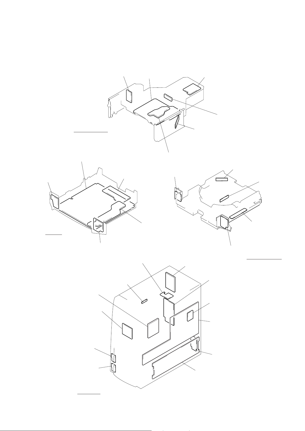
7-1. CIRCUIT BOARDS LOCATION
SECTION 7
DIAGRAMS
LED board
CARRIER ASSY
MA-C22 board
RST board
LDSW board
CARRIER board
CLIP (OUT) board
P LED board
CLIP (IN) board
DISC SENSOR board
FG board
M BOX SW board
MBLD board
CDM-47
SERVICE board
PANEL board
MD LED board
MD LED board
CN board
AC SW board
MBDS board
COVER board
MBMO board
M BOX board
MAIL BOX ASSY
VOLSEL board
FILTER board
RS board
MAIN board
DIP SW board
PS board
MAIN UNIT
7-1
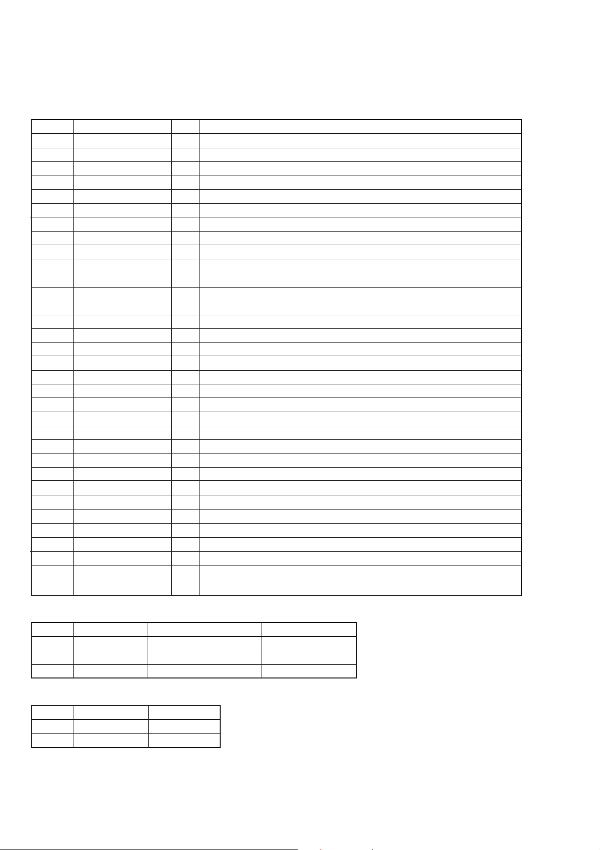
7-2. IC PIN FUNCTION
• IC101 RF AMP (TA2106N) / MA-C22 board
Pin No.
1
2
3
4
5
6
7
8
9
10
11
12
13
14
15
16
17
18
19
20
21
22
23
24
25
26
27
28
29
30
VCC
AGCAD
RFAD0
FNI
FPI
TPI
TNI
MDI
LDO
SEL
TEB
2VRO
TEN
TEO
SBAD
FEO
FEN
SEB
VRO
RFRP
BTC
RFCT
PKC
RFRPIN
RFGO
AGCIN
RFO
GND
RFN2
RFGC
Pin Name
I/O
—
I
I
I
I
I
I
I
O
I
I
O
I
O
O
O
I
I
O
O
I
O
I
I
O
I
O
—
I
I
Function
+5V power supply
RF system AGC AMP gain adjustment input (Not used)
RF AMP gain adjustment input
Main beam AMP input (Detector A,C)
Main beam AMP input (Detector B,D)
Sub beam AMP input (Detector F)
Sub beam AMP input (Detector E)
Monitor photodiode AMP input
Laser diode AMP output
APC circuit ON/OFF signal, LDO pin control input, and bottom/peak detection frequency
switching terminal *1
Tracking error balance control signal input controlled with temary PWM signal
(PWM carrier = 88.2kHz)
Reference voltage (2VREF) output (+4.2V)
Tracking error signal generating AMP inverted phase input
Tracking error signal generating AMP output
Sub beam addition signal output
Focus error signal generating AMP output
Focus error signal generating AMP inverted phase input
RFRP generating circuit mode selection input *2
Reference voltage (VREF) output (+2.1V)
Track count signal generating AMP output
Bottom detection constant adjustment terminal for RFCT signal generation
RFRP signal center level output
Peak detection constant adjustment terminal for RFCT signal generation
Track count signal generating AMP input
RF signal output
RF signal amplitude control AMP input
RF signal generation AMP output
Ground
RF signal generation AMP input
RF amplitude control signal input
RFGC input voltage : 0.5 to 3.5V AGC AMP transfer gain : 0.8 to 1.7 times (typical)
*1
*2
SEL
L
HiZ
H
SEB
L
H
APC circuit
OFF
ON
ON
Bottom detection
ON
OFF
LDO
Connected to VCC Via 1kΩ
Outputs control signal
Outputs control signal
Peak detection
ON
ON
Detection frequency
Low
Low
High
7-2
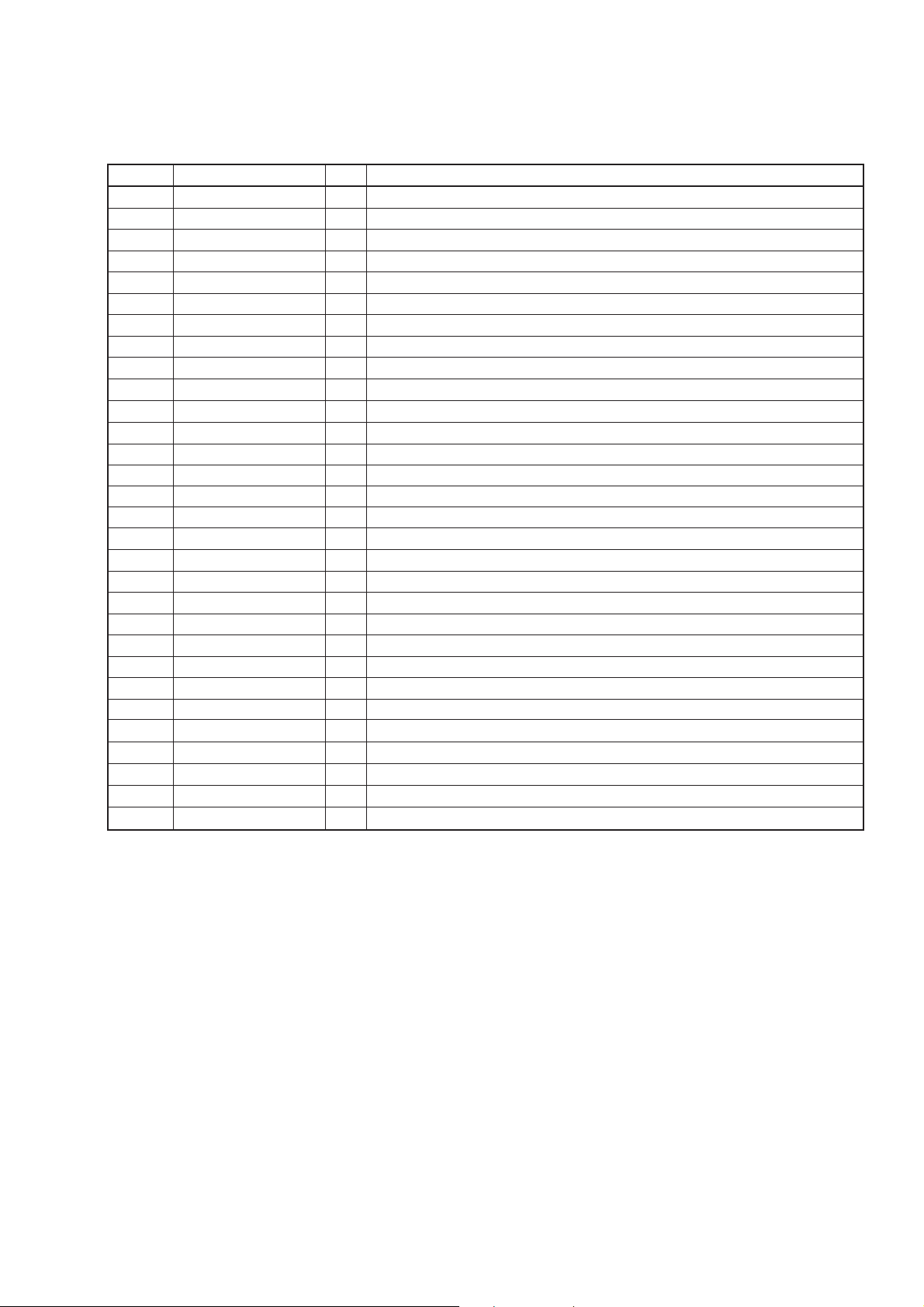
• IC102 2AXIS & Chucking Motor Driver (LA6539M) / MA-C22 board
Pin No.
1
2
3
4
5
6
7
8
9
10
11
12
13
14
15
16
17
18
19
20
21
22
23
24
25
26
27
28
29
30
Pin Name
RF
RF
GND
VIN1
VIN1A
MUTE1
VIN2
VIN2A
VIN3
VIN3A
OUT1
OUT2
VCC
RF
RF
RF
RF
NC
MUTE2
VS2
WOUTWOUT+
VOUTVOUT+
UOUTUOUT+
VS1
VREF1
RF
RF
I/O Function
—
Sub straight (Minimum potential) (not used)
—
Sub straight (Minimum potential) (not used)
—
Ground
I
Chucking motor control signal input
I
Chucking motor control signal input (For adjusting gain)
O
Chucking motor control ON/OFF signal output
I
Focus coil contol signal input
I
Focus coil contol signal input (For adjusting gain)
I
Tracking coil control signal input
I
Tracking coil control signal input (For adjusting gain)
O
Buffer amplifier 1 output (1/2VS1:typ), CH-U output step reference voltage (Not used)
O
Buffer amplifier 2 output (1/2VS2:typ), CH-V,W output step reference voltage (Not used)
—
+12V power supply
—
Sub straight (Minimum potential) (not used)
—
Sub straight (Minimum potential) (not used)
—
Sub straight (Minimum potential) (not used)
—
Sub straight (Minimum potential) (not used)
—
Not used
O
Focus/Tracking coil drive signal ON/OFF control output
I
Focus/Tracking coil drive signal output step power supply (+5V)
O
Tracking coil drive signal reversed output
O
Tracking coil drive signal output
O
Focus coil drive signal reversed output
O
Focus coil drive signal output
O
Chucking motor drive signal reversed output
O
Chucking motor drive signal output
I
Chucking motor drive signal output step power supply (+5V)
—
Level shift circuit reference voltage (+2.1V)
—
Sub straight (Minimum potential) (not used)
—
Sub straight (Minimum potential) (not used)
7-3
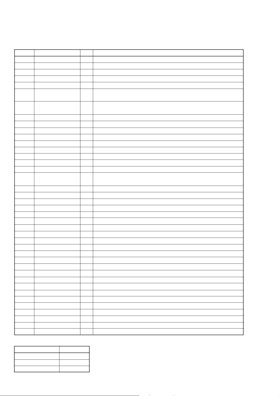
• IC105 Digital Servo & Digital Signal Processor (TC9439F) / MA-C22 board
Pin No.
1
2
3
4
5
6
7
8
9
10
11
12
13
14
15
16
17
18
19
20
21
22
23
24
25
26
27
28
29
30
31
32
33
34
35
36
37
38
39
40
Pin Name
VSS
BCK
AOUT
DOUT
MBOV
IPF
SBOK
CLCK
VDD
VSS
DATA
SFSY
SBSY
SPCK
SPDA
COFS
MONIT
VDD
TESIO0
P2VREF
SPDO
PDOS
PDO
TMAXS
TMAX
LPFN
LPFO
PVREF
VCOREF
VCOF
AVSS
SLCO
RFI
AVDD
RFCT
RFZI
RFRP
FEI
SBAD
TSIN
I/O
—
Ground
O
Bit clock output (1.4122MHz)
O
Audio data output
O
Digital output (Not used)
O
Buffer memory over signal otuput “H”: at over
Outputs the correction flag. This pin becomes “H” when the AOUT output cannot be
O
corrected in the C2 correction
Outputs the CRCC judging result of subcode Q data. This pin becomes “H” when the
O
judging result is OK (Not used)
I/O
Inputs the clock for subcode P-W data reading selectable by command bit
—
+5V power supply
—
Ground
O
Subcode P-W data output
O
Frame sync signal output (Signal in regeneration system)
O
Subcode block sync signal output. “H” at S1 position when subcode sync is detected
O
Clock output for processor status signal reading (176.4kHz) (Not used)
O
Processor status signal output (Not used)
O
Output the frame clock in the correction system (7.35MHz) (Not used)
LSI internal monitoring signal output. DSP internal flag and PLL clock can be monitored
O
by microcomputer commands (Not used)
—
+5V power supply
—
Test pin (Fixed at “L”)
I
Reference voltage input for PLL (+4.2V)
O
VCO center frequency shift signal output
O
Outputs of phase error between EFM signal and PLCK signal (Used in x8 speed mode)
O
Outputs of phase error diference signal between EFM signal and PLCK signal
O
TMAX detection result signal output (Select by command bit TMPS) *1
O
TMAX detection result signal output (Select by command bit TMPS)
I
Inverted amplifier input for low-pass filter
O
Amplifier output for low-pass filter
I
Reference voltage input for PLL (+2.1V)
I
VCO center frequency reference level input (Fixed at “PVREF”)
O
Output from VCO filter
—
Ground (Analog)
O
Data slice level signal output
I
RF signal input
—
+5V power supply (Analog)
I
RFRP signal center level input
I
RFRP zero crossing input
I
RF ripple signal input
I
Focus error signal input
I
Sub beam adding signal input
I
Test pin (Fixed at “VREF”)
Function
*1
TMAX detection result
Longer than ref. period
Shorter than ref. period
Within ref. period
TMAX output
P2VREF
VSS
HiZ
7-4
Pin No. Pin Name
41
42
43
44
45
46
47
48
49
50
51
52
53
54
55
56
57
58
59
60
61
62
63
64
65
66
67
68
69
70
TEI
TEZI
FOO
TRO
VREF
RFGC
TEBC
FMO
FVO
DMO
2VREF
SEL
FLGA
FLGB
FLGC
FLGD
VDD
VSS
IO0
XLOCK
IO2
IO3
/DMOUT
/CKSE
/DACT
/TESIN
TESIO1
VSS
PXI
PXO
I/O
I
Tracking error signal input
I
Tracking error zero crossing signal input
O
Focus servo equalizer signal output
O
Tracking servo equalizer signal output
I
Reference voltage input (+2.1V)
RF amplitude control signal output. The three-value PWM signal is output
O
(PWM carrier = 88.2kHz)
Tracking balance control signal output. The three-value PWM signal is output
O
(PWM carrier : 88.2kHz)
Feed motor equalizer signal output. The three-value PWM signal is output
O
(PWM carrier : 88.2kHz)
Speed error signal or Field search EQ output. The three-value PWM signal is output
O
(PWM carrier = 88.2kHz) (Not used)
O
Disc equalizer signal output. The three-value PWM signal is output (PWM carrier : 88.2kHz)
I
Reference voltage input (+4.2V)
APC circuit ON/OFF signal output.
O
“Hi-Z” is output when UHS = “L” at laser ON, or “H” is output when UHS = “H”
External flag output for internal signal monitoring.
O
TEZC, /FOON, /FOK or RFZC signal is selectable by command
External flag output for internal signal monitoring.
O
TRON, /FOON, /DMON or RFZC signal is selectable by command
External flag output for internal signal monitoring.
O
TRON, /TSSR, /FOK or /SRCH signal is selectable by command
External flag output for internal signal monitoring.
O
TRON, /DMON, /HYS or /SHC signal is selectable by command
—
+5V power supply
—
Ground
O
RF equalizer control signal output
I/O
PLL LOCK “L” PLL UNLOCK “H”
I/O
Not used
I/O
Not used
This pins sets field equalizer binary PWM output mode from pins 100 and 101,ans also
I
sets disc equalizer binary PWM output mode from pins 102 and 103 “L”: active
(Not used)
I
Crystal selection pin “H”: 16.934MHz, “L”: 33.8688MHz (Fixed at “L”)
I
Test pin (Not used)
I
Test pin (Fixed at “L”)
I
Test pin (Fixed at “L”)
—
Ground
I
DSP clock oscillating circuit input (50.8032MHz)
O
DSP clock oscillating circuit output (50.8032MHz)
Function
7-5
 Loading...