

Sony CDE67 Service Manual
CD-E67
SERVICE MANUAL
No. S3320CDE67///
MINI COMPONENT SYSTEM
MODEL CD-E67
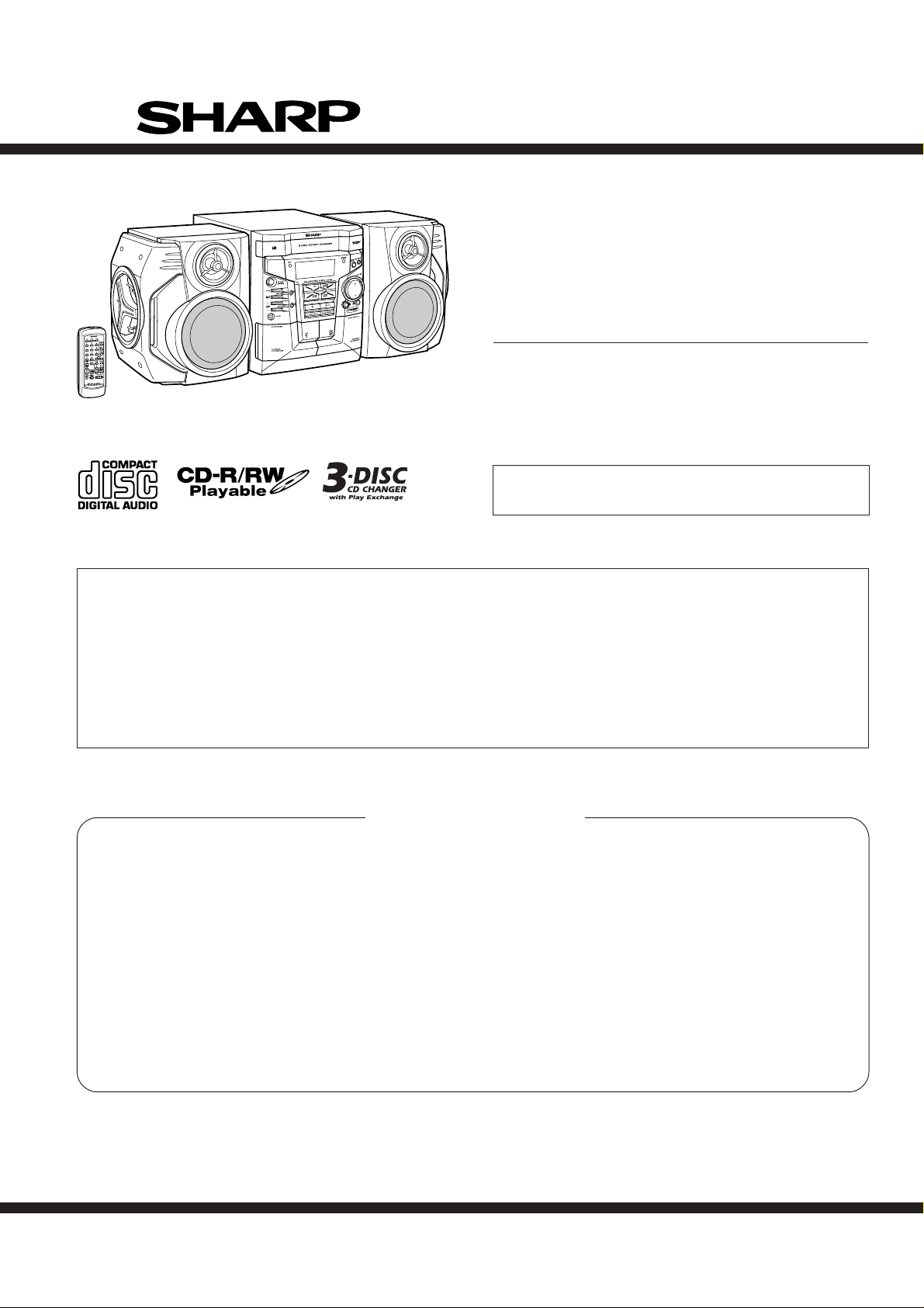
CD-E67 Mini Component System consisting of CD-E67
(main unit) and CP-E67 (speaker system).
• In the interests of user-safety the set should be restored to its
original condition and only parts identical to those specified be
used.
This Service Manual is for the CD-E67, which is a minor-modification model of the CD-E700/CD-E77, This manual, therefore,
describes only the changed points from the service manual.
Please refer to the CD-E700/CD-E77, service manual (No. S1301CDE700//) together with this manual.
CD-E700/CD-E77
Page
REMOVING AND REINSTALLING THE MAIN PARTS .......................................................................................................... 9
ADJUSTMENT....................................................................................................................................................................... 10
TROUBLESHOOTING........................................................................................................................................................... 37
FUNCTION TABLE OF IC ..................................................................................................................................................... 41
CONTENTS
Page
IMPORTANT SERVICE NOTES........................................................................................................................................ 2
SPECIFICATIONS ............................................................................................................................................................. 2
NAMES OF PARTS ........................................................................................................................................................... 3
DISASSEMBLY.................................................................................................................................................................. 5
NOTES ON SCHEMATIC DIAGRAM ................................................................................................................................ 8
TYPES OF TRANSISTOR AND LED................................................................................................................................. 8
BLOCK DIAGRAM ............................................................................................................................................................. 9
SCHEMATIC DIAGRAM / WIRING SIDE OF P.W.BOARD............................................................................................. 12
VOLTAGE ........................................................................................................................................................................ 29
WAVEFORMS OF CD CIRCUIT...................................................................................................................................... 30
FL DISPLAY..................................................................................................................................................................... 31
REPLACEMENT PARTS LIST/EXPLODED VIEW
PACKING OF THE SET
SHARP CORPORATION
This document has been published to be used
for after sales service only.
The contents are subject to change without notice.
CD-E67
IMPORTANT SERVICE NOTES
BEFORE RETURNING THE AUDIO PRODUCT
(Fire & Shock Hazard)
Before returning the audio product to the user, perform the
following safety checks.
1. Inspect all lead dress to make certain that leads are not
pinched or that hardware is not lodged between the chassis
and other metal parts in the audio product.
2. Inspect all protective devices such as insulating materials,
cabinet, terminal board, adjustment and compartment covers
or shields, mechanical insulators etc.
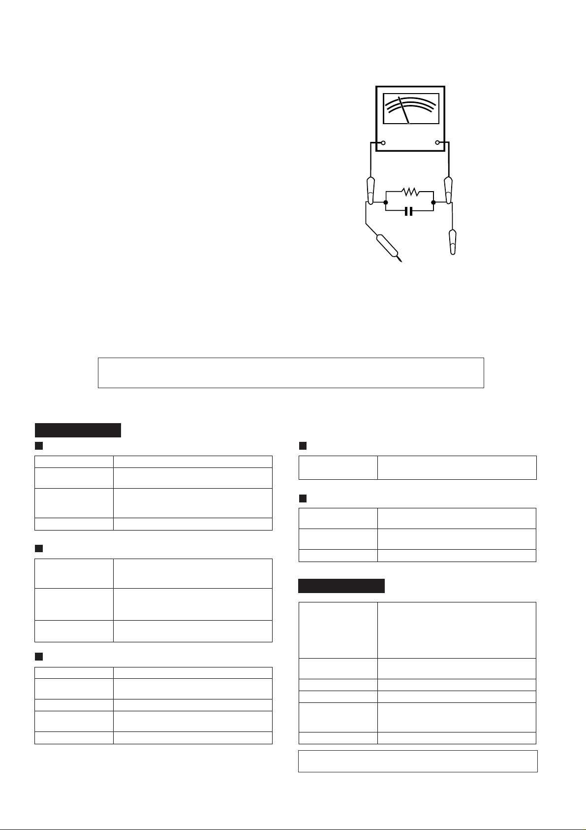
3. To be sure that no shock hazard exists, check for leakage
current in the following manner.
* Plug the AC line cord directly into a 120 volt AC outlet.
* Using two clip leads, connect a 1.5 kohm, 10 watt resistor
paralleled by a 0.15 µF capacitor in series with all exposed
metal cabinet parts and a known earth ground, such as
conduit or electrical ground connected to earth ground.
* Use a VTVM or VOM with 1000 ohm per volt, or higher,
sensitivity to measure the AC voltage drop across the
resistor (See diagram).
* Connect the resistor connection to all exposed metal parts
having a return path to the chassis (antenna, metal cabinet,
screw heads, knobs and control shafts, escutcheon, etc.)
and measure the AC voltage drop across the resistor.
VTVM
AC SCALE
1.5 kohms
10 W
0.15 µF
TO EXPOSED
TEST PROBE
METAL PARTS
CONNECT TO
KNOWN EARTH
GROUND
All check must be repeated with the AC line cord plug connection
reversed.
Any reading of 0.3 volt RMS (this corresponds to 0.2 milliamp.
AC.) or more is excessive and indicates a potential shock
hazard which must be corrected before returning the audio
product to the owner.
FOR A COMPLETE DESCRIPTION OF THE OPERATION OF THIS UNIT, PLEASE REFER
TO THE OPERATION MANUAL.
SPECIFICATIONS
CD-E67
General
Power source AC 120 V, 60 Hz
Power
consumption
Dimensions Width: 10-5/8" (270 mm)
Weight 16.7 lbs. (7.6 kg)
Amplifier
Output power 100 watts minimum RMS per channel into 6
Output terminals Speakers: 6 ohms
Input terminals Video/Auxiliary (audio signal): 500 mV/47 k
CD player
Type 3-disc multi-play compact disc player
Signal readout Non-contact, 3-beam semiconductor laser
D/A converter 1-bit D/A converter
Frequency
response
Dynamic range 90 dB (1 kHz)
166 W
Height: 12" (305 mm)
Depth: 13-1/2" (342 mm)
ohms from 60 Hz to 20 kHz, 10% total harmonic distortion
Headphones: 16 - 50 ohms (recommended:
32 ohms)
ohms
pickup
20 - 20,000 Hz
Tuner
Frequency range FM: 87.5 - 108 MHz
AM: 530 - 1,720 kHz
Cassette deck
Frequency
response
Signal/noise ratio 55 dB (TAPE 1, playback)
Wow and flutter 0.3 % (WRMS)
CP-E67
Type
Maximum input
power
Rated input power 100 W
Impedance 6 ohms
Dimensions Width: 9-11/16" (246 mm)
Weight 7.9 lbs. (3.6 kg)/each
50 - 14,000 Hz (normal tape)
50 dB (TAPE 2, recording/playback)
2-way 2-speaker system with passive radiator
2" (5 cm) tweeter
5-1/8" (13 cm) woofer
5-1/8" (13 cm) passive radiator
200 W
Height: 12" (305 mm)
Depth: 9-1/4" (235 mm)
Specifications for this model are subject to change without prior
notice
– 2 –
CD-E67
CD-E67
NAMES OF PARTS
Front panel
1. Disc Tray
2. Timer Set Indicator
3. Memory/Set Button
4. Power On/Stand-by Button
5. Clock Button
6. Timer/Sleep Button
7. Tuning and Time Up Button
8. Tuning and Time Down Button
9. Headphone Jack
10. Tape 2 Record Pause Button
11. Tape 1 Cassette Compartment
12. Equalizer Mode Select Button
13. Extra Bass/Demo Mode Button
14. Volume Up and Down Buttons
15. Disc Tray Open/Close Button
16. Disc Skip Button
17. Tape 2 Cassette Compartment
18. CD Button
19. Tape (1 2) Button
20. CD or Tape Stop Button
21. CD Track Down or Fast Reverse, Tape 2 Rewind,
Tuner Preset Down Button
22. Tuner (Band) Button
23. Video/Auxiliary Button
24. CD Play or Repeat, Tape Play Button
25. CD Track Up or Fast Forward, Tape 2 Fast Forward,
Tuner Preset Up Button
10
11
1
2
3
4
5
6
7
8
9
12
13
14
15
16
17
18
19
20
21
22
23
24
25
Display
1. Disc Number Indicators
2. CD Play Indicator
3. Tape Play Indicator
4. FM Stereo Mode Indicator
5. FM Stereo Receiving Indicator
6. Memory Indicator
7. Extra Bass Indicator
8. Timer Recording Indicator
9. Timer Play Indicator
10. CD Pause Indicator
11. CD Repeat Play Indicator
12. Tape Record Indicator
13. Sleep Indicator
Rear panel
1. Cooling Fan
2. AC Power Cord
3. FM/AM Loop Antenna Jack
4. Video/Auxiliary (Audio Signal) Input Jacks
5. Speaker Terminals
Note:
This product is equipped with a cooling fan inside, which begins to
run at a specified volume level for better heat radiation.
214567
3
8
9
131210 11
3
1
4
5
– 3 –
2
CD-E67
CD-E67
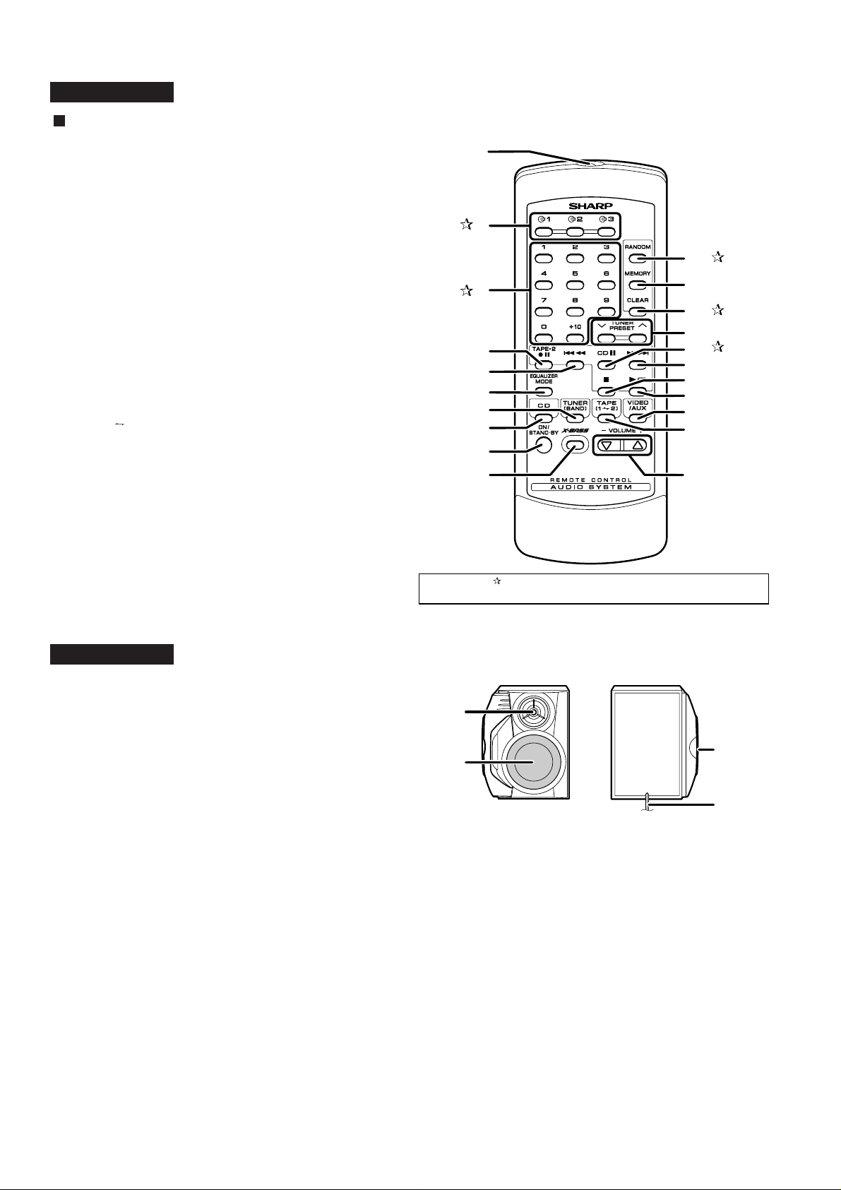
Remote control
1. Remote Control Transmitter
2. Disc Number Select Buttons
3. Direct Search Buttons
4. Tape 2 Record Pause Button
5. CD Track Down or Fast Reverse,
Tape 2 Rewind Button
6. Equalizer Mode Select Button
7. Tuner (Band) Button
8. CD Button
9. Power On/Stand-by Button
10. Extra Bass Button
11. CD Random Button
12. CD Memory Button
13. Program Clear Button
14. Tuner Preset Up and Down Buttons
15. CD Pause Button
16. CD Track Up or Fast Forward,
Tape 2 Fast Forward Button
17. CD or Tape Stop Button
18. CD Play or Repeat, Tape Play Button
19. Video/Auxiliary Button
20. Tape (1 2) Button
21. Volume Up and Down Buttons
10
1
2
11
3
12
13
14
4
5
6
7
8
15
16
17
18
19
20
9
21
CP-E67
1. Tweeter
2. Woofer
3. Passive Radiator
4. Speaker Wire
Buttons with " " mark in the illustration or highlighted in bold on the
left can be operated on the remote control only.
1
3
2
4
– 4 –
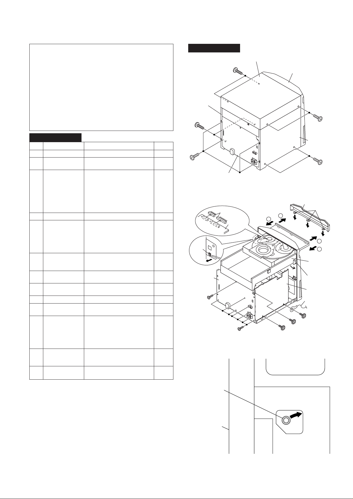
DISASSEMBLY
Lock Lever
CD Player Unit
(Bottom View)
(B1)x2
ø3x10mm
(A1)x2
ø3x12mm
(A1)x2
ø3x12mm
(B1)x2
ø3x10mm
(B1)x4
ø3x10mm
Rear
Panel
Side Panel
(Right)
Side Panel
(Left)
Top Cabinet
Front
Panel
Caution on Disassembly
Follow the below-mentioned notes when disassembling
the unit and reassembling it, to keep it safe and ensure
excellent performance:
1. Take cassette tape and compact disc out of the unit.
2. Be sure to remove the power supply plug from the wall
outlet before starting to disassemble the unit.
3. Take off nylon bands or wire holders where they need to
be removed when disassembling the unit. After servicing
the unit, be sure to rearrange the leads where they were
before disassembling.
4. Take sufficient care on static electricity of integrated
circuits and other circuits when servicing.
CD-E67
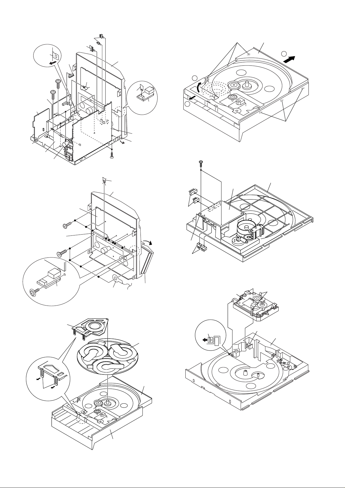
STEP
10 Turntable 1. Hook........................ (K1) x2 6-3
11 Loading Tray 1.
12 CD Servo PWB 1. Screw ...................... (M1) x2 6-5
13 CD Mechanism 1. Hook........................ (N1) x2 6-6
Note 1: How to open the changer manually. (Fig. 5-3)
1. In this state, turn fully the lock lever in the arrow direction through
2. After that, push forward the Loading tray.
REMOVAL
1 Top Cabinet 1. Screw ...................... (A1) x4 5-1
2 Side Panel 1. Screw ...................... (B1) x8 5-1
(Left/Right)
3 CD Tray Cover/ 1.
CD Player Unit
4 Rear Panel 1. Screw ...................... (D1) x8 5-2
5 Main PWB 1. Screw ...................... (E1) x2 6-1
6 Front Panel 1. Screw .......................(F1) x2 6-1
7 Display PWB 1. Screw ...................... (G1) x9 6-2
8 Tape Mechanism 1. Open the cassette holder. 6-2
9
Headphones PWB
(Note 2) 2. Hook........................ (M2) x1
the hole on the loading tray bottom.
tray cover, and close.
(Note 1)
2. Screw ...................... (C1) x1
3. Hook........................ (C2) x3
4. Hook........................ (C3) x2
5. Socket ..................... (C4) x2
2. Fan Cover ............... (E2) x1
3. Screw ...................... (E3) x4
4. Socket ..................... (E4) x4 6-1
5. Flat Cable ............... (E5) x1
6. Flat Wire.................. (E6) x1
2. Hook......................... (F2) x2
3. Flat Wire...................(F3) x1
2. Flat Cable ............... (G2) x1
2. Screw...................... (H1) x5
1. Screw ....................... (J1) x1 6-2
2. Stabilizer Holder ..... (K2) x1
2.
3. Socket ..................... (M3) x4
2. Hook........................ (N2) x2
PROCEDURE
Turn on the power supply, open
the disc tray, take out the CD
Turn fully the lock lever in the
arrow direction.
Push the loading tray backward
to engage the claw with the
groove and remove it in the
direction of the arrow
...
(L1) x6
FIGURE
5-2
5-2, 6-1
5-3
6-4
(C3)x1
Pull
Rear
Panel
(C1)x1
ø3x10mm
CD-E67
(C4)x2
CD Servo
PWB
Figure 5-1
(D1)x7
ø3x10mm
Figure 5-2
2
(E3)x1
ø3x10mm
CD Tray Cover
1
CD-E67
(C2)x3
CD Player
Unit
(C3)x1
Main PWB
Lug Wire
(E3)x1
ø3x10mm
(D1)x1
ø3x10mm
1
2
Note 2:
1. After removing the connector for the optical pickup from the
connector, wrap the conductive aluminium foil around the front end
of the connector so as to protect the optical pickup from electrostatic damage.
Note 3:
1. Be careful not to break the claw of the CD mechanism.
2. When fining back the cam gear assembly, let it lock by front
movement.
Figure 5-3
– 5 –
CD-E67
(F2)x1
(E3)x2
ø3x6mm
(E1)x2
ø3x6mm
Power PWB
Transformer
PWB
(E4)x1
(E2)x1
Fan Motor
(E4)x1
(E4)x2
(E5)x1
(F3)x1
Figure 6-1
Front
Panel
(F1)x2
ø3x10mm
(G2)x1
Front Panel
(E6)x1
Headphones
PWB
Main PWB
(F2)x1
(L1)x3
Loading Tray
3
2
1
(L1)x3
Figure 6-4
(M1)x2
ø3x10mm
Loading
CD Servo
PWB
Tray
(G1)x9
ø3x10mm
Tape
Mechanism
(H1)x5
ø3x10mm
(J1)x1
ø3x10mm
Display PWB
Headphones
PWB
(K2)x1
Lug Wire
Figure 6-2
Open
Cassette
Holder
Turntable
(M3)x2
(M2)x1
(M3)x2
(N1)x1
CD
Mechanism
Figure 6-5
(N2)x2
(N1)x1
Loading Tray
(K1)x2
Loading
Tray
Figure 6-6
CD Player Unit
Figure 6-3
– 6 –
CP-E67
(A3)x4
ø4x16mm
(B2)x4
ø4x16mm
(C1)x2
ø3x12mm
Speaker Box
Woofer
Tweeter
Passive
Radiator
STEP
REMOVAL
1 Passive Radiator 1. Screw ...................... (A1) x4 7-1
2. Side Panel .............. (A2) x1
3. Screw ...................... (A3) x4 7-3
2 Woofer 1. Front Panel ............. (B1) x1 7-2
2. Screw ...................... (B2) x4 7-3
3 Tweeter 1. Screw ...................... (C1) x2 7-3
PROCEDURE
Speaker Box
(A2)x1
CD-E67
FIGURE
Screwdriver
Figure 7-3
(A1)x4
ø4x35mm
Figure 7-1
(B1)x1
Speaker Box
Driver should
be pried away
from Speaker Box.
Figure 7-2
– 7 –
CD-E67
NOTES ON SCHEMATIC DIAGRAM
• Resistor:
To differentiate the units of resistors, such symbol as K and
M are used: the symbol K means 1000 ohm and the symbol
M means 1000 kohm and the resistor without any symbol is
ohm-type resistor. Besides, the one with “Fusible” is a fuse
type.
• Capacitor:
To indicate the unit of capacitor, a symbol P is used: this
symbol P means pico-farad and the unit of the capacitor
without such a symbol is microfarad. As to electrolytic
capacitor, the expression “capacitance/withstand voltage”
is used.
(CH), (TH), (RH), (UJ): Temperature compensation
(ML): Mylar type
(P.P.): Polypropylene type
• Schematic diagram and Wiring Side of P.W.Board for this
model are subject to change for improvement without prior
notice.
• The indicated voltage in each section is the one measured
by Digital Multimeter between such a section and the chassis with no signal given.
1. In the tuner section,
indicates AM
indicates FM stereo
2. In the main section, a tape is being played back.
3. In the deck section, a tape is being played back.
( ) indicates the record state.
4. In the power section, a tape is being played back.
5. In the CD section, the CD is stopped.
• Parts marked with “ 1 ” ( ) are important for
maintaining the safety of the set. Be sure to replace these
parts with specified ones for maintaining the safety and
performance of the set.
REF. NO
SW1 OPEN/CLOSE ON—OFF
SW2 CLAMP ON—OFF
SW3 DISC NUMBER ON—OFF
SW4 PICKUP IN ON—OFF
SW701 POWER ON—OFF
SW702 MEMORY/SET ON—OFF
SW703 REC PAUSE ON—OFF
SW704 TUNING/TIME DOWN ON—OFF
SW705 TUNING/TIME UP ON—OFF
SW706
SW707
SW711
SW712 TUNER (BAND) ON—OFF
TIMER/SLEEP
CLOCK
CD
DESCRIPTION
POSITION
ON—OFF
ON—OFF
ON—OFF
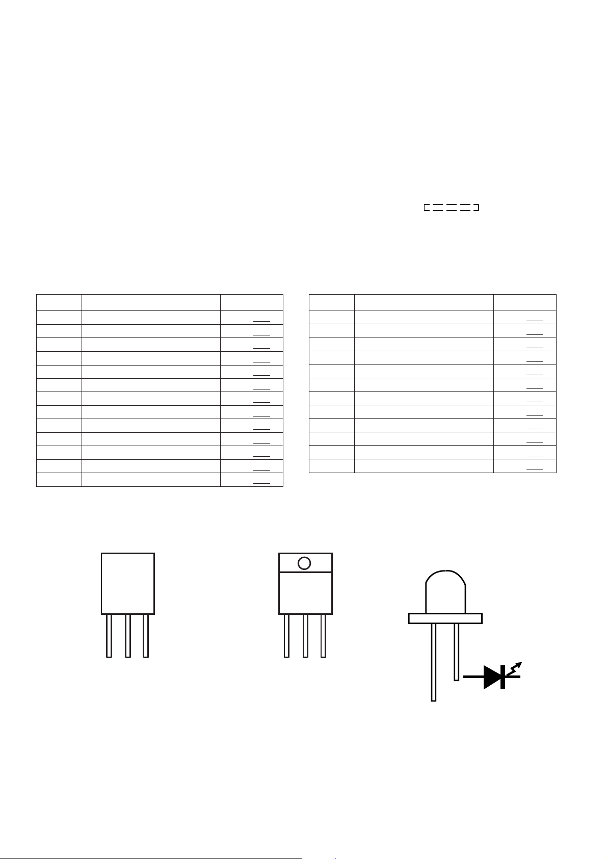
TYPES OF TRANSISTOR AND LED
FRONT
VIEW
REF. NO DESCRIPTION POSITION
SW713 VIDEO/AUX ON—OFF
SW714 TAPE ON—OFF
SW715 STOP ON—OFF
SW716 PLAY/REPEAT ON—OFF
SW717 FAST FORWARD/PRESET UP ON—OFF
SW718 FAST REWIND/PRESET DOWN ON—OFF
SW721 X-BASS/DEMO ON—OFF
SW722 EQUALIZER ON—OFF
SW723 OPEN/CLOSE ON—OFF
SW724 DISC SKIP ON—OFF
SW725 VOLUME UP ON—OFF
SW726 VOLUME DOWN ON—OFF
FRONT
VIEW
FRONT
VIEW
E C B
(S) (G) (D)
(1) (2) (3)
KRC102 M
KRC104 M
KTA1266 GR
KTA1271 Y
KTA1273 Y
KTA1274 Y
KTC3194 Y
KTC3199 GR
KTC3200 GR
KTC3203 Y
B C E
KTC2026
– 8 –
304VT2E1
A503BC2E
CD-E67
XL1
16.9344 MHz
Q4
+3.3V
CONSTANT
VOLTAGE
TO MAIN SECTION
(+B8)
D_GND
A5V
(+B4)
+6.5V
8 7 1 2 3 4 5 6
CNP5
(+B7)
R-CH
AGND
L-CH
D5V
DGND
45
42
CE
61
CL
62
DI
63
DO
64
*WRQ
65
*RES
66
DRF
67
LCHO
RCHO
LC78646E
CD SERVO
XOUT
48
XIN
49
LVDD
41 18 10 9 8 7 5
+3.3V
38
VDD
VVDD
RFVDD
ADAVDD
XVDD68VDD5
47 46
IC1
RVDD
Q1
FIN2
FIN1
LASER
DRIVER
TO DISPLAY SECTION
WRQ
DRF CEDOCLDI
71 70
CONT3
CONT2
CONT 5
SLDO
SPDO
LDD
LDS
TIN2
TIN1
80 79 77
SW1
+6.5V
+5V
OPEN/CLOSE
1
VCC2
22
12
CLAMP SW
O/C_SW
CD RES
FD0
TD0
DISC NO
10 3 1 9 8 7 6 52 4
CNP6
75
69
57
56
55
51
50
43
44
40
37
28
19
6
26
23
22
21
20
SW3
CLAMP
15 13 1 7 24
SLDO
DISC
NUMBER
M3
M
T/T UP/DOWN
+
28 27
SPO
LOADING MOTOR
–
CNS4
CNP4
BI4
SW2
2 3 1 4 6 5
2 3 1 4 6 5
2 3 1 4 6 5
FD
TO
IC2
LA6574H
FOCUS/TRACKING/
SPIN/SLED
DRIVER
3 2
30
29
26
+5V (+B7)
PICKUP UNIT
+3.3V
COIL
TRACKING
FOCUS COIL
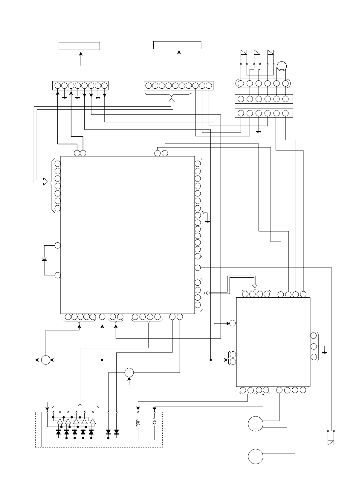
Figure 9 BLOCK DIAGRAM (1/3)
– 9 –
M1
SPINDLE
MOTOR
M2
SLED
MOTOR
M
M
9
8 7 6 5 4
10 11
+
–
+
–
IC
SW4
PICKUP
IN
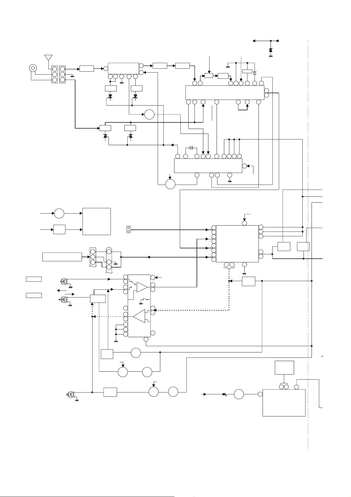
CD-E67
AM LOOP
ANTENNA
+B3
+B3
TAPE 1
P.B. HEAD
TAPE 2
REC./P.B.
HEAD
FM
ANTENNA
1
1
2
2
3
3
CNP301
MOTOR
DRIVER
Q706
Q707
Q708
SOLENOID
DRIVER
CNP5
FROM CD SECTION
L-CH
R-CH
REC.
P.B.
L-CH
R-CH
AC BIAS
ERASE
HEAD
BF301
B.P.F
FM RF
TAPE
MECHANISM
ASS'Y
2
3
CNS601
SWITCHING
Q101~
Q104
IC301
TA7358AP
FM FRONT END
8
7
FM
OSC
OSC BUFF
AM BAND
COVERAGE
6
9
FM
OSC
1
4
5
3
L312 T301
AM TRACKING
T303 T306
IC302
LC72131
PLL(TUNER)
JK690
VIDEO/AUX
IN
L
AUX
R
BI601
R
11
3
4
L
L(T1)
1
P.B
24
R(T1)
L(T2)
2
23
R(T2)
POP REDUCE
L REC
R REC
SWITCHING
Q105
Q106
+B5
Q111
L103
BIAS
OSC
6
9
16
11
12
15
Q112
SWITCHING
H/N
T1/T2
REC
NOR/
HIGH
T1/T2
Q114
SWITCHING
Q113
SWITCHING
Q302
FM+B
19
13
4
21
7
18
10
Q109
+B6
FM IF
T302
SWITCHING
L
R
CF303
T351
AM IF
21
AM MIX
AM OSC IN
AM OSC OUT
AM RF IN
20
FM
X352
4.5 MHz
1
OSC
TUNER
22 111615
7
TAPE
CD
L
R
L
R
L
R
L
R
VT
+B5
Q360
+B5
PB
RECRL
IC101
AN7345K
PLAYBACK AND RECORD
ALC
/PLAYBACK AMP.
+B5
Q110
BIAS
+B5
+B6
ZD351
10.7 MHz
CF351
17
FM
DET
FM+B
MPXIN
5.1V
X351
456 kHz
13
VCO
FM/AM
450 kHz
CF352
7
+B6
985
4
GND
AM IF
FM/AM
OUT
1821 12162324
IC303
STEREO
LA1832S
FM IF DET./
FM MPX./
AM IF
CLK
DO
DI
CE
5436
21
IC601
7
18
DRIVER
LED
Q710
17
+B5
23
CLK
3
Q107
Q108
MUTING
+B5
DI
CE
1
2
24
21
4
63
MO/ST
FM/AM
9
10
9
16
10
15
LC75341
11
14
AUDIO PROCESSOR
12
13
LED703,
LED704
+B5
14
L
MO/ST
R
15
–20dB
ATT
Q601
Q602
R
L
REC/PLAY
JOG701
JOG
VOLUME
49 50
47
IC701
IX0553AW
SYSTEM
MICROCOMPUTER
(2/2)
Q603
Q604
T1/T2
BIAS
MUTE
SYSTEM
VF1
Figure 10 BLOCK DIAGRAM (2/3)
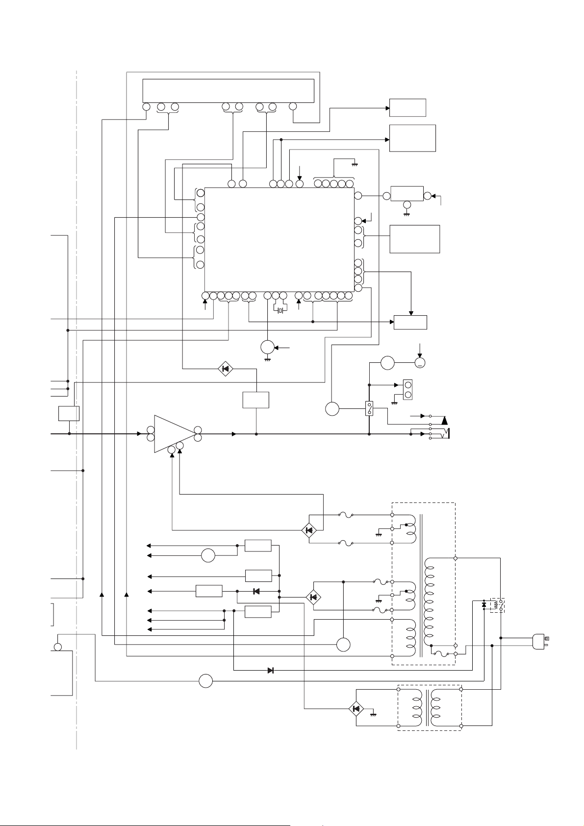
– 10 –
CD-E67
FL701
FL DISPLAY
~
34
29
51
19
~
~
35
45
41
+B10
TO CD
SECTION
TAPE
MECHANISM
ASS'Y
Q603
Q604
/PLAY
MUTE
SYSTEM
SP DET.
D905~D907
IC901
STK40212S
POWER AMP.
1
L
15
R
9
8
72
~
78
79
80
~~
85
86
100
+B10
7
10
38 52 51
VLOAD
MICROCOMPUTER
VDD
12456 78
L-OUT
R-OUT
54
IC701
IX0553AW
SYSTEM
RESET
Q709
Q901~
Q904
55
40
46
48
25 13 30
VDD
AVDD
(1/2)
RESET
XL701
4.19 MHz
VDD
11 12 1 0 16 1 7 20 21 22 23 24
+B10
+B10
SP RELAY
ON-OFF
~
CLK
CEDIDO
Q905
39
+B10
34
33
~
31
37
26
15
41
FAN MOTOR
DRIVER
RL914
RX701
REMOTE
1
SENSOR
2
KEY
SW701-SW707
SW711-SW718
SW721-SW726
TO CD
SECTION
Q906
+B3
HEADPHONES
3
+B10
+B7
M901
M
FAN
MOTOR
SO901
SPEAKER
TERMINAL
JK701
47
UTER
T1/T2
BIAS
VF1
M_13V
+B3
LD+7V
+B4
A_10V
+B5
+B10
+B7
+B8
+B9
UNSW_5.6V
D_5V
A_5V
SW_5V
–VF
VF2
IC853, IC854
VOLTAGE REGULATOR
AC_RLY
-B2
+B2
IC855
VOLTAGE
REGULATOR
IC854
AN78L05
Q841
RELAY
DRIVER
IC851
KIA7812AP
VOLTAGE
REGULATOR
IC851
IC852
D853
IC853
KIA7805AP
D855
D802
IC852
KIA7810AP
VOLTAGE
REGULATOR
D803,
D804
F802
5A/125V
F801
5A/125V
Q801
D842~
D845
F803
2A/125V
F804
2A/125V
VOLTAGE
REGULATOR
PT801
MAIN POWER
TRANSFORMER
T.F.
PT841
SUB POWER
TRANSFORMER
RL841
AC POWER
SUPPLY CORD
AC 120 V, 60 Hz
Figure 11 BLOCK DIAGRAM (3/3)
– 11 –
CD-E67
/
0
0
0
0
47/25
10K
/
1
1
ALC
3
C
2
0
R
A
B
C
D
E
F
G
CNP5
P21 12 - D
TO CD SERVO PWB
TAPE 1
PLAYBACK HEAD
R-CHL-CH
ERASE
HEAD
R-CH
L-CH
TAPE 2
RECORD/
PLAYBACK HEAD
BI601
CNS601
1
2
3
4
5
6
7
8
P16 1 - E~H
1
2
3
1
2
3
4
5
6
7
R-CH
1
A_GND
3
L-CH
4
CD_GND
5
CD_+B
6
7
D_GND
8
LD+7V
9
L-CH
10
( A_GND)
GND
11
12
13
D_GND
14
15
16
17
18
19
20
TO POWER SECTION
21
22
23
24
25
26
T1_R
1
A_GND
2
T1_L
3
CNP101
M_GND
1
ERASE
2
T2_R2
3
A_GND
4
T2_R1
5
T2_L1
6
T2_L2
7
CNP102
+B
R_CH
LD+7V
+B
(DRIVER)
A_5V
D_5V
(CD_GND)
GND
CD(A_GND)
(D_GND)
GND
+B_PROTECT
M_+13.5V
A_+10V
SW_5V
SP_DET
SP_RLY
(M_GND)
GND
FM SIGNAL
PLAYBACK SIGNAL
RECORD SIGNAL
CD SIGNAL
VIDEO SIGNAL
Q603
KTC3199 GR
SYSTEM MUTE
Q604
KTC3199 GR
SYSTEM MUTE
C640
22/50
C102
560P
C101
560P
C104
180P
C103
180P
R617
2.2K
R616
2.2K
SWITCHING
0V
0V
0V
0V
0V
0V
KTC3200 GR
SWITCHING
+B
+B
R619
330
R618
330
+B
+B
+B
+B
+B
4.7K
Q601
R615
4.7K
R614
Q602
R620
22K
Q102
KTC3200 GR
0.7V
0.7V
Q104
KTC3200 GR
SWITCHING
SWITCHING
Q103
KTC3200 GR
0.7V
R105
3.3K
0.7V
R103
2.2K
Q101
R605
10K
R613
390
KTC3199 GR
R610
KTC3199 GR
R612
390
C639
1/50
S_MUTE
R104
2.2K
R106
3.3K
R611
2.2K
2.2K
C609
1/50
R109
0V
R107
R110 R108
4.7K
47K
9.3V
9.3V
0V
R621
22K
0V
Q112
KTA1266 GR
R102
1K
R101
1K
47K
0V
0V
4.7K
Q106
Q105
KTC3199 GR
0V
SWITCHING
+B
C602
0.022
R607
3.9K
C611
0.0022
C629
0.001
R363
6.8K
C625
0.0022
8.6V
SWITCHING
560P
C106
SWITCHING
KTC3199 GR
560P
C105
C653
220P
C601
220/16
C652
C607
0.15
C613
1/50
C615
4.7/50
C619
1/50
C623
1/50
R609
1.2K
R147
10K
10K
R146
R148
4.7K
R112
15K
R114
1K
R
L
R113
1K
IC101
AN7345K
PLAYBACK
AND
RECORD/
PLAYBACK
AMP.
R111
15K
C108
330P
C107
330P
C651
220P
C605
(ML)
0.1
C617
1/50
C621
1/50
C112
100/25
C114
0.033
23
C113
0.033
C111
100/25
R115
56
DI
1
CE
220P
2
VSS
3
LOUT
4
–
+
LBASS
5
LTRE
6
LIN
7
LSEL0
8
L4
9
L3
10
L2
11
L1
12
AUDIO PROCESSOR
SWITCHING
Q113
L
KRC104 M
3.4V
2
3
0V
1
0V
1
3.4V
2
0V
3
Q114
KRC104 M
SWITCHING
R116
56
C116
560P
C118
47/25
R118
R120
100K
C110
330P
–
+
112K
Hich=T1
112K
+
–
4516
C109
330P
R117 R119
100K 3.9K
C115
C117
560P
47/25
CCB
INTERFACE
–
+
–
+
AUX
DECK
TUNER
CD
IC601
LC75341
+B
C141
100/16
10K
R122
R124
5.6K
3.9K
R123
5.6K
10K
R121
–
+
+
–
+
–
+
–
–20dBATT
R149
C120
0.0022
IC101
AN7345K
C121
0.022
C119
0.0022
150
R150
+
C150
68K
R128
5.6K
–
47/25
C143
R127
24
CLK
23
VDD
VREF
22
ROUT
21
RBASS
20
RTRE
19
RIN
18
RSEL0
17
R4
16
R3
15
R2
14
R1
13
MUTING
0V
0V
KTC3199 GR
270P
C124
4.7K
R126
Hich=CHROME
78
R129
5.6K
3.3/50
270P
C123
4.7K
R130
R131
C614
R136
220K
0.7V
Q108
1.5K
C126
22/50
C125
22/50
1.5K
C606
0.1
1/50
R132
–
+
+
–
R
R138
10K
C128
R133
+B
(ML)
C622
1/50
100
0.022
56K
56K
100
0.022
C127
+B
C130
R602
R60
C618
1/50
C62
0.0033
161718192021222324
9
0.0033
C129
1K
C6
22
1/5
C6
1/5
R134
C1
47
C
0.
C132
1
H
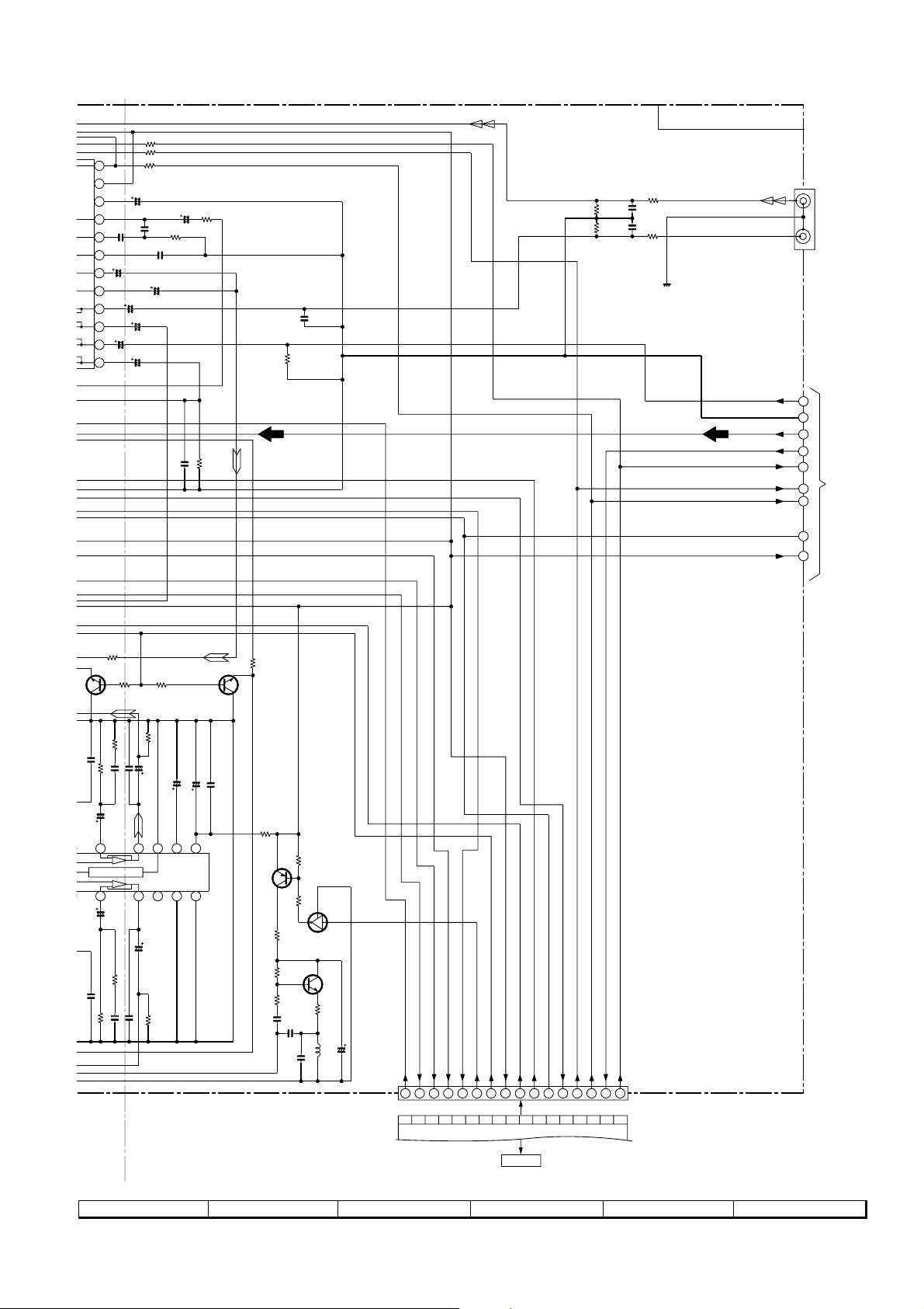
• NOTES ON SCHEMATIC DIAGRAM can be found on page 8.
1
23456
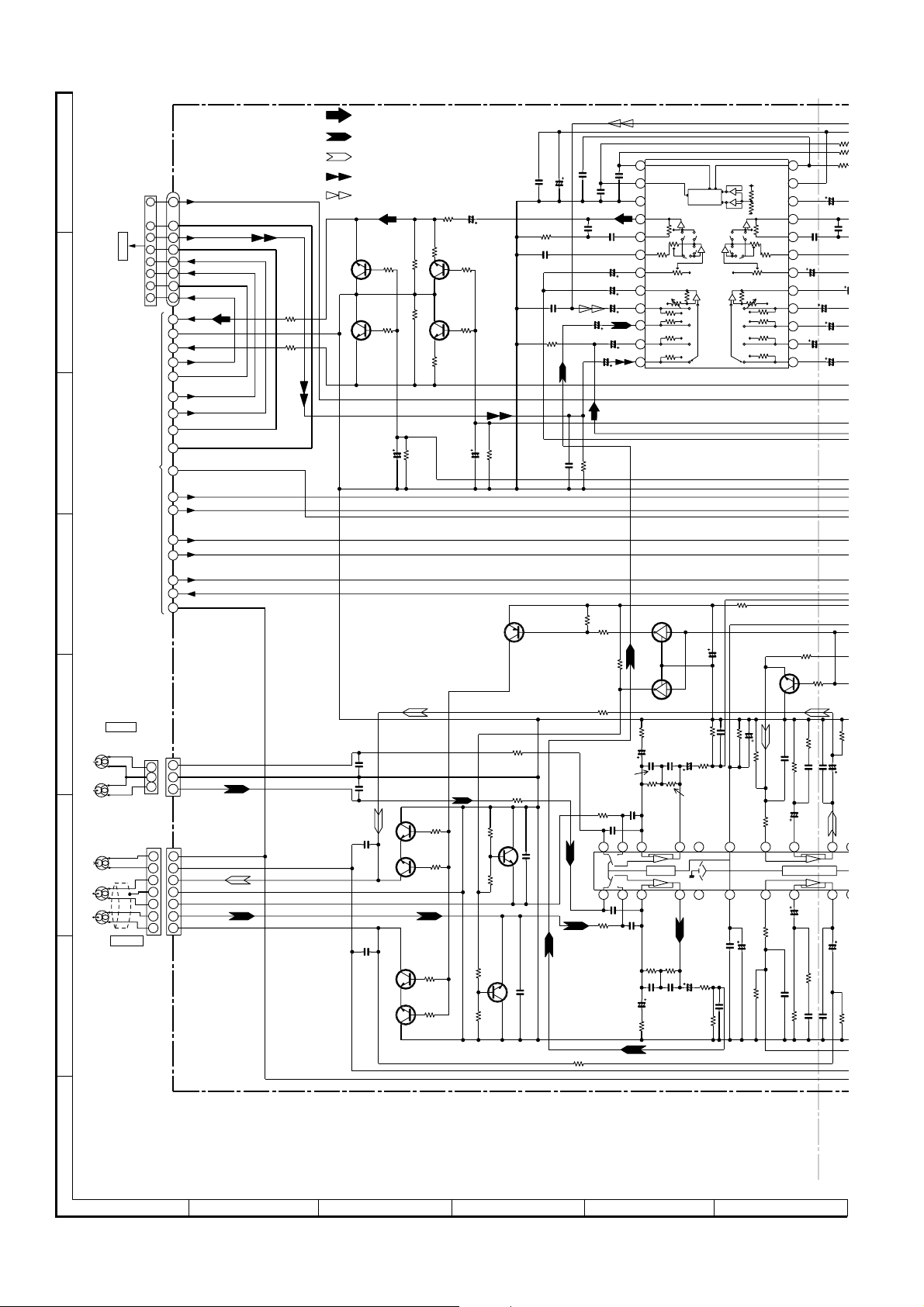
Figure 12 SCHEMATIC DIAGRAM (1/10)
– 12 –
CD-E67
C124
C123
CLK
VDD
REF
OUT
ASS
RIN
EL0
TRE
R601
1K
1K
R602
24
R603
+B
C606
0.1
C614
1/50
(ML)
C622
1/50
+B
C618
1/50
C620
1/50
C624
1/50
1K
C603
22/50
C608
0.15
C612
0.0022
R606
3.9K
C616
4.7/50
C610
1/50
C626
0.0022
R604
10K
R608
1.2K
C630
0.001
R364
6.8K
23
22
21
20
19
18
17
R4
16
R3
15
R2
14
R1
13
+B
C691
R691
390P
5.6K
C690
R690
390P
5.6K
+B
MAIN PWB-A1(1/3)
R693
33K
R692
33K
CHASSIS
TUN_R
A GND
TUN_L
D_GND
+B
A_+10V
CLK
L-CH
JK690
VIDEO/AUX
IN
R-CH
1
2
3
DO
4
CE
5
DI
6
7
P15 10~12 - H
TO TUNER SECTION
8
9
MUTING
0V
0V
KTC3199 GR
270P
R130
Hich=CHROME
K
8
129
.6K
270P
R131
R136
220K
0.7V
Q108
1.5K
C126
22/50
C125
22/50
1.5K
R
R132
C128
–
+
+
–
R133
R138
10K
100
0.022
100
C130
0.022
56K
56K
C127
REC_R
R139
10K
KTC3199 GR
10K
R134
0.0033
9101112
C131
47/25
0.0033
C129
C132
R135
10K
47/25
Nor/CrO2
ALC
22/50
C133
RIPPLE
ALC
220/10
C134
1314151617
0.7V
Q107
Vcc
GND
MUTING
0.022
C135
0V
REC_L
R137
220K
R158
220
Q109
KTA1266 GR
SWITCHING
0V
R141
82
R142
(1/2W)
47K
R143
C137
0.047(ML)
+B
+B
4.7K
11.6V
R144
C138
0.0082
R140
47K
11.6V
213
KRC104 M
0V
22K
Q110
0V
0V
0V
R145
4.7
BIAS
0V
Q111
KTC3203 Y
REC/PLAY
T_BIAS
BIAS OSC.
T-T1 T2
+B
+B
A_+10V
D1
CE
DO
CLK
+B
+B
D_GND
C139
0.039(ML)
7
8 9 10 11 12
L103
47/25
C140
330 µH
1
SW_5V
SP_DET
SP_RLY
–20dB
12345
A_+10V
REC/PLAY
T_BIAS
M_+13.5V
6 7 8 9 10 11 12 13 14 15 16
CNP701A
P18 1 - F
TO DISPLAY PWB
T_T1/T2
D_GND
S_MUTE
+B-PROTECT
CLK
DI
CE
DO
CNP701B
16
FFC701
Figure 13 SCHEMATIC DIAGRAM (2/10)
– 13 –
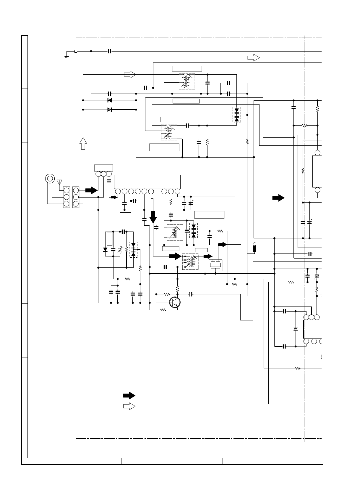
CD-E67
3
CE
C350 0 022
0
C394
C362
L
A
B
C
D
E
F
AM LOOP
ANTENNA
FM
ANTENNA
1
2
3 3
BAND PASS FILTER
CNP301
1
2
C302
0.001
C338 0.001
D301 DS1SS133
D302 DS1SS133
BF301
1 2 3
C303
10P(CH)
D305
DS1SS133
C308
4.7P
(CH)
C314
FM FRONT END
C304
0.01
C309
0.001
FM RF
L312
R311
100K
R314
22
0.0047
C315
0.0047
C316
C323
0.022
IC301
TA7358AP
4
3 2 1
5
C305
4.7P
(CH)
C320
0.001VD302
SVC211C
R313
C317
0.022
T306
AM OSC.
AM BAND
COVERAGE fL
6
7
R302
10
C311
18P
C310
15P(CH)
FM OSC.
C312
0.022
33K
R325
47K
0.001
R327
33
AM TRACKING
AM ANTENNA
8
9
C306
C324
4.7P(UJ)
T301
R322
KTC3194 Y
OSC BUFFER
T303
C335
560P
0.022
T302
680
Q302
C334
22P
(UJ)
C307
10/50
COVERAGE fL
C313
FM IF
C318
100P
C330
FM BAND
VD303
SVC211C
22P
(CH)
1
15P
(UJ)
VD301
SVC348S
68K
R323
R309
10K
3
2
C331
0.047
C332
0.022
CF303
+B
R316
4.7K
10K
R336
TP301
+B
+B
C342
0.022
R382
C381
12P(CH)
X352
4.5 MHz
C382
15P(CH)
0.022
150
R358
3.9K
5.6K
R351
C351 0.022
C352 10/50
C393 0.0
C397
R381
21 20
22
X IN X OUT
1 2
10K
R365
24
AM OSC OUT
FM IF IN
1
10K
C
1
VSS
AOUT
G
FM SIGNAL
AM SIGNAL
H
• NOTES ON SCHEMATIC DIAGRAM can be found on page 8.
1
23456
Figure 14 SCHEMATIC DIAGRAM (3/10)
– 14 –
+B
+B
R375
470
R374 1K
 Loading...