

Page 1
CDC-R937/X937
SERVICE MANUAL
Ver 1.1 2004. 04
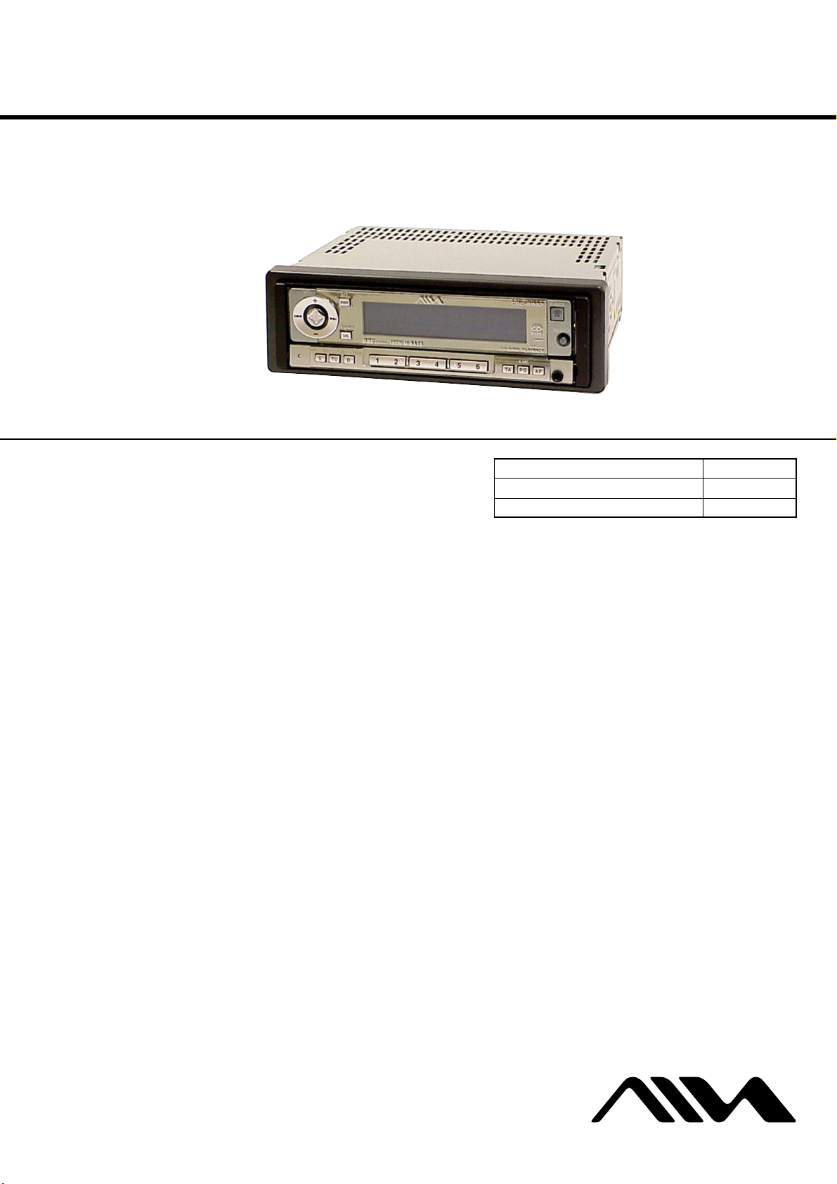
Photo: CDC-R937
• The CD section have no adjustment.
SPECIFICATIONS
US Model
Canadian Model
CDC-X937
AEP Model
UK Model
CDC-R937
Model Name Using Similar Mechanism NEW
CD Drive Mechanism Type MG-930B-185
Optical Pick-up Name OPTIMA-752B
RADIO SECTION
(FM)
Frequency Range: 87.5 MHz – 108 MHz
Intermediate frequency: 10.7 MHz (CDC-R937)
Usable Sensitivity: 12.7 dBf
50 dB Quieting Sensitivity: 17.2 dBf
IF Rejection: 100 dB
Frequency Response: 30 Hz – 15,000 Hz
S/N Ratio: 67 dB (CDC-R937)
70 dB (CDC-X937)
Stereo Separation: 35 dB at 1 kHz
Alternate Channel Selectivity: 98 dB
Capture Ratio: 3 dB
(AM) (CDC-X937)
Frequency Range: 530 kHz – 1,710 kHz
Usable Sensitivity: 30 µV (30 dB)
(MW) (CDC-R937)
Frequency Range: 531 kHz – 1,602 kHz
Intermediate frequency: 10.71 MHz/450 kHz
Usable Sensitivity: 30 µV (30 dB)
(LW) (CDC-R937)
Frequency Range: 144 kHz – 288 kHz (1 kHz/9 kHz step)
Intermediate frequency: 10.71 MHz/450 kHz
Usable Sensitivity: 30 µV (30 dB)
CD SECTION
Frequency Response: 17 Hz – 20 kHz +0/–3 dB
Dynamic Range: More than 92 dB
Channel Separation: More than 60 dB
S/N Ratio: More than 90 dB
Wow/Flutter: Unmeasurable
AUDIO SECTION
Max. Power Output: 45 W × 4 channels
AUX IN Input
Input sensitivity (load impedance) AUX IN: 300 mV (10 kΩ)
– Continued on next page –
FM/AM COMPACT DISC PLAYER
CDC-X937
9-877-344-02
2004D04-1
© 2004. 04
FM/MW/LW COMPACT DISC PLAYER
CDC-R937
Sony Corporation
e Vehicle Company
Published by Sony Engineering Corporation
1
Page 2
CDC-R937/X937
GENERAL
Power-Supply Voltage: 14.4 V (11 to 16 V allowable),
Load Impedance: 4 Ω
Tone Control: Bass ±10 dB at 100 Hz,
Preamp Output Voltage (load impedance): 2.2 V (10 kΩ)
Installed size: 182 (W) × 53 (H) × 155 (D) mm
Supplied Accessory: Carrying case (1)
CARD REMOTE CONTROL
Dimensions: Approx. 33 (W) × 85 (H) × 7.5 (D) mm
Weight: Approx. 20 g (0.7 oz.) (including battery)
• Specifications and external appearance are subject
to change without notice due to product improvement.
DC, negative ground
Treble ±10 dB at 10 kHz
(7 1/4 (W) × 2 1/8 (H) × 6 1/8 (D) inches)
(1 5/16 (W) × 3 3/8 (H) × 5/16 (D) inches)
SERVICE NOTES
NOTES ON HANDLING THE OPTICAL PICK-UP BLOCK
OR BASE UNIT
The laser diode in the optical pick-up block may suffer electrostatic
breakdown because of the potential difference generated by the
charged electrostatic load, etc. on clothing and the human body.
During repair, pay attention to electrostatic breakdown and also use
the procedure in the printed matter which is included in the repair
parts.
The flexible board is easily damaged and should be handled with
care.
NOTES ON LASER DIODE EMISSION CHECK
The laser beam on this model is concentrated so as to be focused on
the disc reflective surface by the objective lens in the optical pickup block. Therefore, when checking the laser diode emission, observe from more than 30 cm away from the objective lens.
Notes on Chip Component Replacement
• Never reuse a disconnected chip component.
• Notice that the minus side of a tantalum capacitor may be dam-
aged by heat.
CDC-X937:
CAUTION
Use of controls or adjustments or performance of procedures
other than those specified herein may result in hazardous
radiation exposure.
CDC-R937:
CAUTION
Use of controls or adjustments or performance of procedures other
than those specified herein may result in hazardous radiation
exposure.
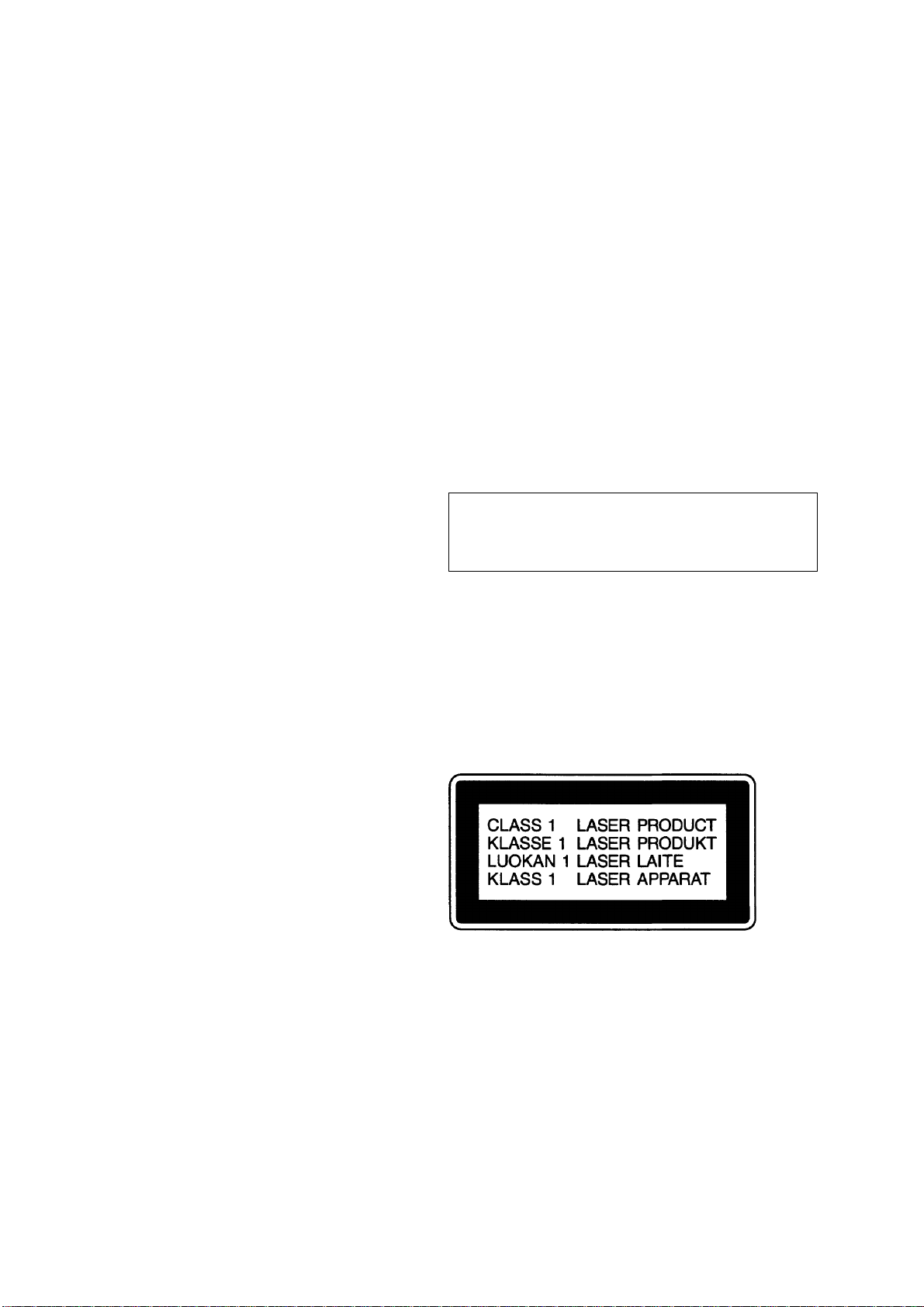
This compact disc player is classified as a CLASS 1 LASER
product. The CLASS 1 LASER PRODUCT label is located on the
exterior.
SAFETY-RELATED COMPONENT WARNING!!
COMPONENTS IDENTIFIED BY MARK 0 OR DOTTED LINE
WITH MARK 0 ON THE SCHEMATIC DIAGRAMS AND IN
THE PARTS LIST ARE CRITICAL TO SAFE OPERATION.
REPLACE THESE COMPONENTS WITH SONY P ARTS WHOSE
PART NUMBERS APPEAR AS SHOWN IN THIS MANUAL OR
IN SUPPLEMENTS PUBLISHED BY SONY.
2
ATTENTION AU COMPOSANT AYANT RAPPORT
À LA SÉCURITÉ!!
LES COMPOSANTS IDENTIFIÉS P AR UNE MARQUE 0 SUR LES
DIAGRAMMES SCHÉMATIQUES ET LA LISTE DES PIÈCES
SONT CRITIQUES POUR LA SÉCURITÉ DE FONCTIONNEMENT.
NE REMPLACER CES COMPOSANTS QUE PAR DES PIÈCES
SONY DONT LES NUMÉROS SONT DONNÉS DANS CE MANUEL
OU DANS LES SUPPLÉMENTS PUBLIÉS PAR SONY.
Page 3

TABLE OF CONTENTS
1. GENERAL
Connections (CDC-X937) ....................................................... 4
Connections (CDC-R937) ....................................................... 5
2. DISASSEMBLY
2-1. Base (Around) ..................................................................... 8
2-2. CD Mechanism Block ......................................................... 8
2-3. Main Board Section ............................................................ 9
2-4. Main Board ......................................................................... 9
2-5. Heat Sink (CT) .................................................................. 10
2-6. Motor (SVX) Assy ............................................................ 10
2-7. Sub Board.......................................................................... 11
2-8. Servo Board....................................................................... 11
2-9. Floating Block Assy .......................................................... 12
2-10. Lever Assy (CD Up Holder CNF).....................................12
2-11. Lever (CD Roller) Sub Assy ............................................. 13
2-12. Lever Assy (CD Holder) ................................................... 13
2-13. Motor (Sled) Sub Assy...................................................... 14
2-14. Pick-up Sub Assy .............................................................. 14
CDC-R937/X937
3. ELECTRICAL ADJUSTMENT.................................... 15
4. DIAGRAMS
4-1. IC Pin Descriptions ........................................................... 16
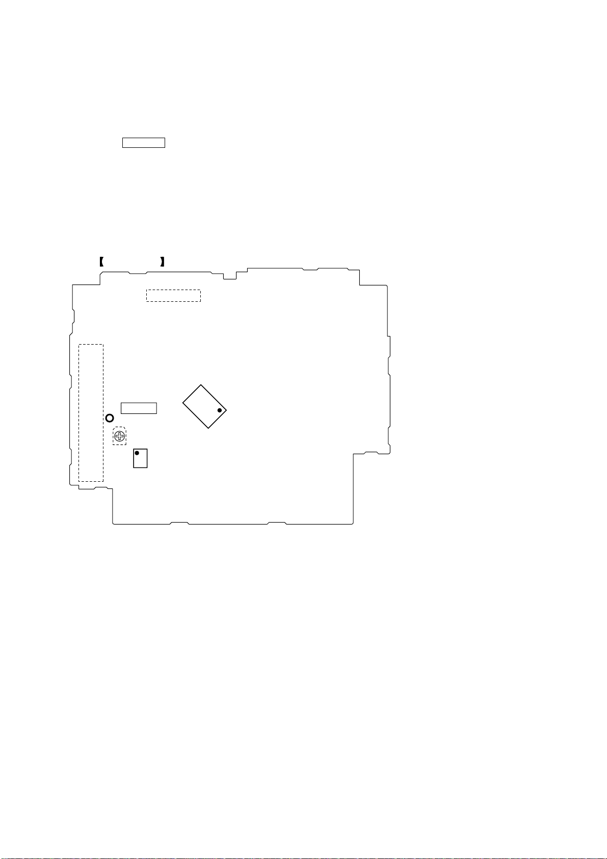
4-2. Circuit Boards Location .................................................... 19
4-3. Block Diagram –CD Section–........................................... 20
4-4. Block Diagram –Main Section–........................................ 21
4-5. Block Diagram –Front Section–........................................ 22
4-6. Schematic Diagram –CD Mechanism Section– ................ 23
4-7. Printed Wiring Boards –CD Mechanism Section–............ 24
4-8. Printed Wiring Board –Main Section– .............................. 26
4-9. Schematic Diagram –Main Section (1/2)– ........................ 28
4-10. Schematic Diagram –Main Section (2/2)– ........................ 29
4-11. Printed Wiring Boards –Key Section– .............................. 30
4-12. Schematic Diagram –Key Section–................................... 31
4-13. Printed Wiring Boards –Front Section– ............................ 32
4-14. Schematic Diagrams –Front Section– ............................... 33
4-15. IC Block Diagrams............................................................ 34
5. EXPLODED VIEWS
5-1. Chassis Section ................................................................. 36
5-2. Panel Section .....................................................................37
5-3. Front Section ..................................................................... 38
5-4. CD Mechanism Section (1) ............................................... 39
5-5. CD Mechanism Section (2) ............................................... 40
6. ELECTRICAL PARTS LIST ........................................ 41
3
Page 4
CDC-R937/X937
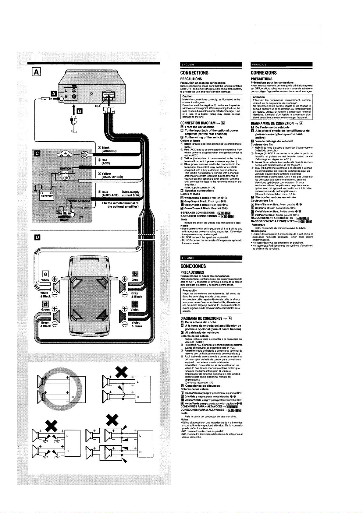
CONNECTIONS (CDC-X937)
SECTION 1
GENERAL
This section is extracted
from instruction manual.
4
Page 5
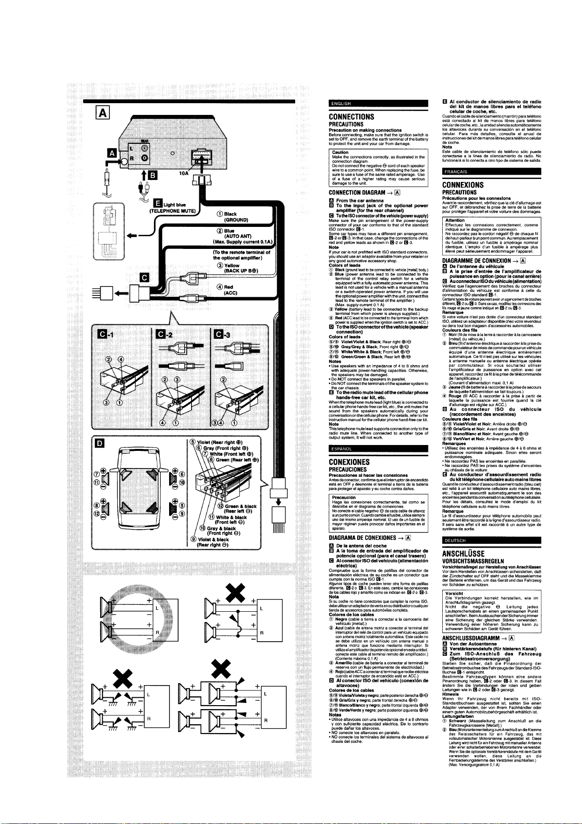
CONNECTIONS (CDC-R937)
CDC-R937/X937
5
Page 6
CDC-R937/X937
6
Page 7
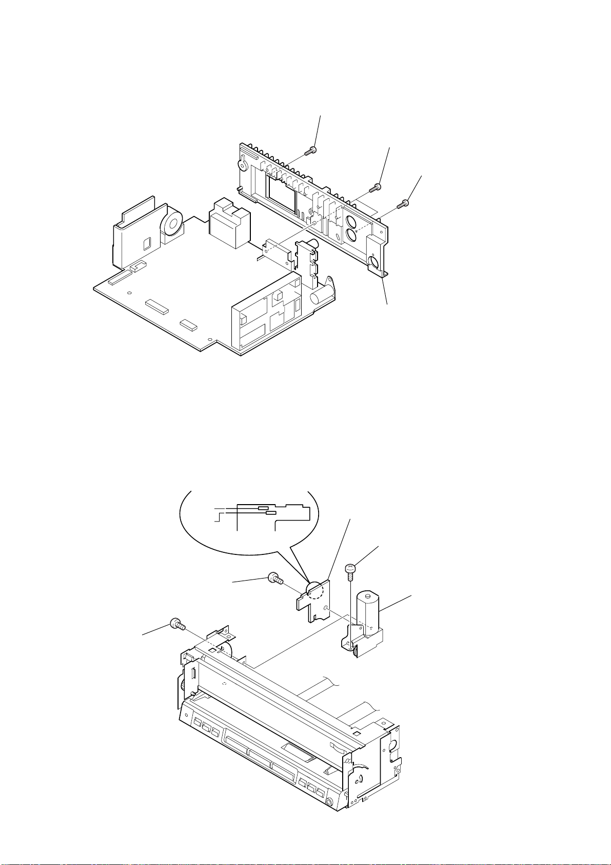
SECTION 2
DISASSEMBLY
Note : This set can be disassemble according to the following sequence.
SET
2-1. BASE (AROUND)
(Page 8)
2-2. CD MECHANISM BLOCK
(Page 8)
CDC-R937/X937
2-3. MAIN BOARD SECTION
(Page 9)
2-4. MAIN BOARD
(Page 9)
2-5. HEAT SINK (CT)
(Page 10)
2-6. MOTOR (SVX) ASSY
2-14. PICK-UP SUB ASSY
2-12. LEVER ASSY (CD HOLDER)
2-13. MOTOR (SLED) SUB ASSY
(Page 10)
(Page 14)
(Page 13)
(Page 14)
2-7. SUB BOARD
(Page 11)
2-8. SERVO BOARD
(Page 11)
2-9. FLOATING BLOCK ASSY
(Page 12)
2-10. LEVER ASSY (CD UP HOLDER CNF)
(Page 12)
2-11. LEVER (CD ROLLER) SUB SSY
(Page 13)
7
Page 8
CDC-R937/X937
)
Note : Follow the disassembly procedure in the numerical order given.
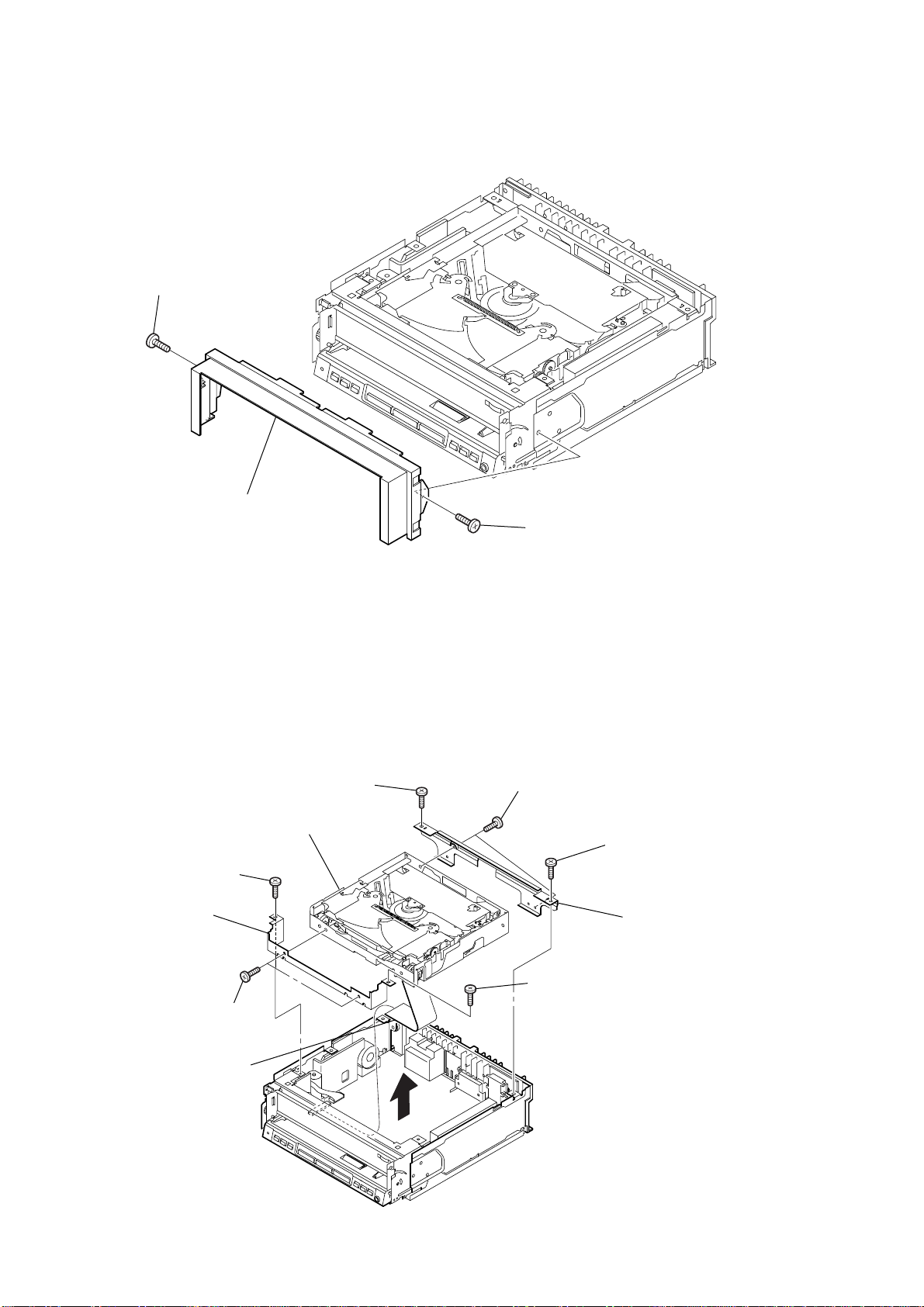
2-1. BASE (AROUND)
2
screw (TH 2.6x4)
3
2-2. CD MECHANISM BLOCK
qa
CD mechanism block
3
screw
(
0
bracket (CD)
TH 2.6x4
)
base (around)
2
screw
(+
PTP 2.6x4
1
screw (TH 2.6x4)
)
7
(+
two
screws
PTP 2.6x4
)
1
screw
(+
PTP 2.6x4
8
holder (CD mecha
)
4
screw
(
two screws (TH 2.6x4)
9
6
CON771
TH 2.6x4
5
)
8
Page 9
2-3. MAIN BOARD SECTION
8
two
screws
(M
2.6x3
)
7
CON721
4
Removal the solder.
brown
black
6
CON702
5
CON701
CDC-R937/X937
qs
MAIN board section
1
(+
screw
PTP 2.6x4
)
2-4. MAIN BOARD
6
screw
(+
PTT 2.6x5
qa
front section
)
3
sheet (PWB)
7
L chassis
5
(+
9
two
(M
2
cover
0
two ground point screws (+PTT 2.6x6)
screw
PTT 2.6x6
)
4
screw
(+
PTT 2.6x6
screws
2.6x3
)
)
3
Removal the solder.
9
MAIN board
8
R chassis
2
Removal the solder.
1
Removal
the solder.
9
Page 10
CDC-R937/X937
y
2-5. HEAT SINK (CT)
1
(+
screw
BTT 2.6x8
)
2
two
(+
4
heat sink (CT)
screws
P 3x12
3
(+
)
screw
PTT 2.6x8
)
2-6. MOTOR (SVX) ASSY
1
screw
PTT 2x3
(+
)
5
(+
4
Removal the solders.
black
brown
screw
PTT 2x3
)
6
SENSOR board
2
screw
(+
PTT 2x3
3
motor (SVX) ass
)
10
Page 11
2-7. SUB BOARD
1
Removal the solders.
2
(+
screw
P 1.4x2
CDC-R937/X937
)
3
SUB board
2-8. SERVO BOARD
blue
brown
black
5
PIC2 FLEXIBLE board
1
Removal the solders.
gray
white
red
black
2
(+
screw
PTT 2x3
black
yellow
4
SERVO board
)
3
two
(M
screws
1.7x5
)
green
red
11
Page 12

CDC-R937/X937
w
2-9. FLOATING BLOCK ASSY
1
8
claw
qs
oil damper
tension spring
0
2
tension spring
qd
floating block aasy
3
tension spring
9
7
claw
qa
oil damper
4
tension spring
5
tension spring
2-10. LEVER ASSY (CD UP HOLDER CNF)
1
screw
P 1.4x2
(+
2
leaf spring (roller)
)
6
claw
5
lever assy (CD up holder CNF)
4
tension spring
12
3
special scre
Page 13
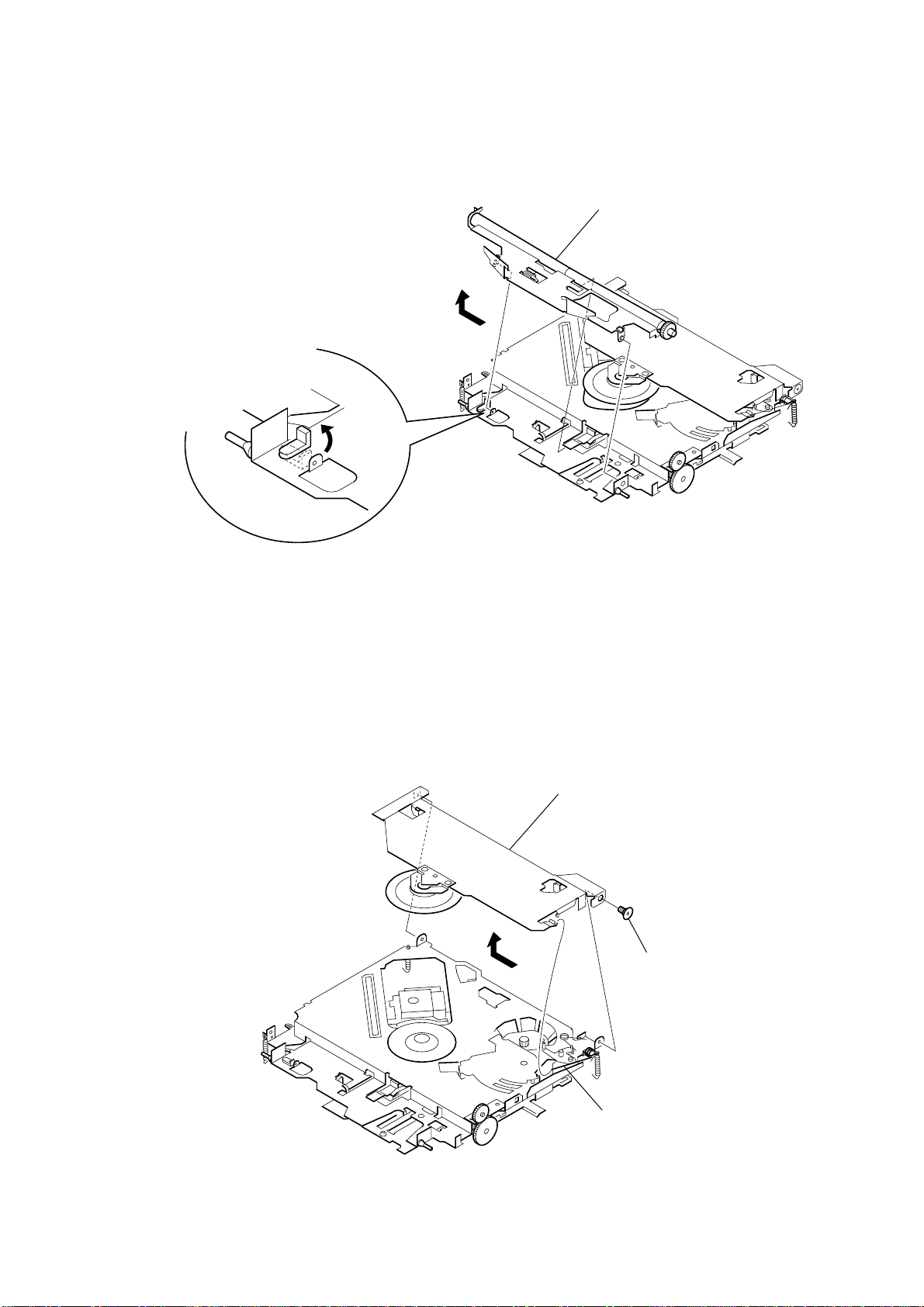
2-11. LEVER (CD ROLLER) SUB ASSY
1
2
3
lever (CD roller) sub assy
CDC-R937/X937
2-12. LEVER ASSY (CD HOLDER)
3
4
lever assy (CD holder)
2
special screw
1
torsion spring
13
Page 14
CDC-R937/X937
y
y
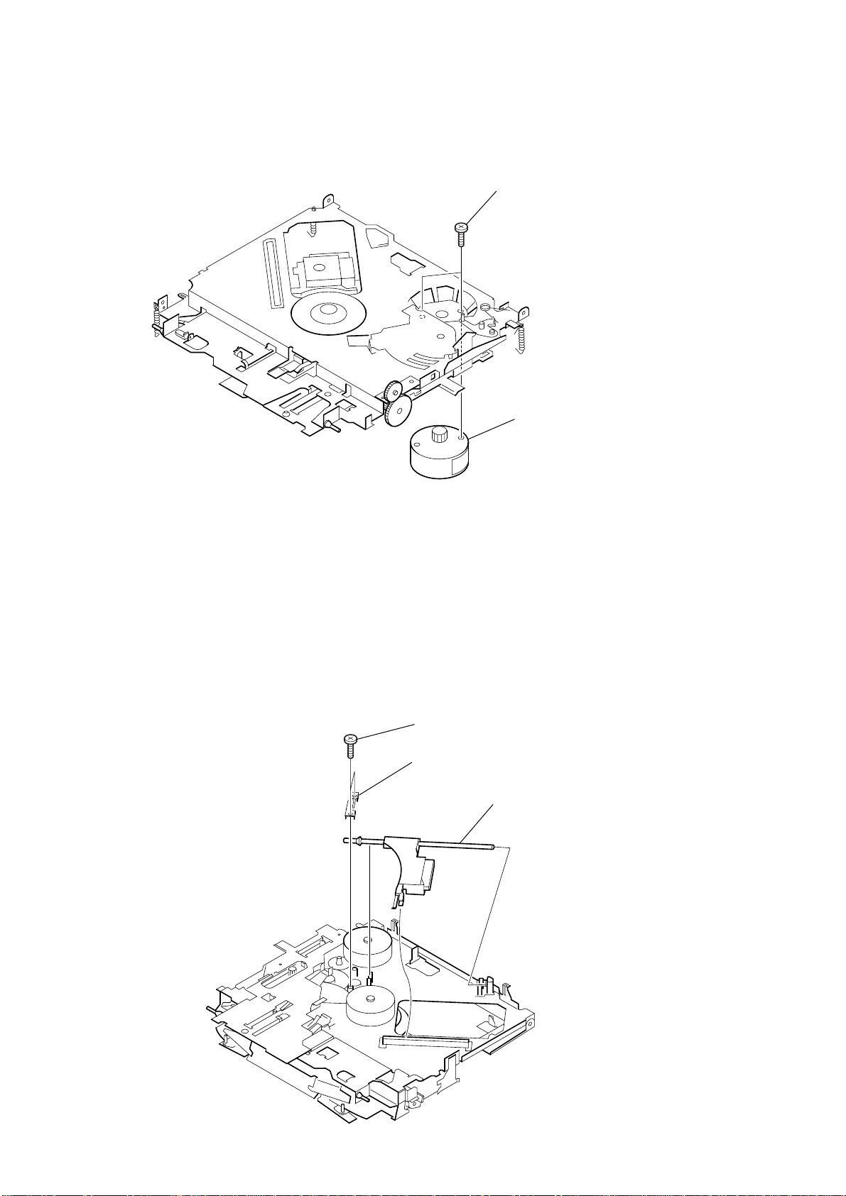
2-13. MOTOR (SLED) SUB ASSY
1
screw
P 1.7x2
(+
2
)
motor (sled) sub ass
2-14. PICK-UP SUB ASSY
1
two
screws
B 1.4x5
(+
2
leaf spring
)
3
pick-up sub ass
14
Page 15
SECTION 3
ELECTRICAL ADJUSTMENT
RDS Adjustment (CDC-R937 only)
Setting:98 MHz
31 dBµV (EMF)
1 kHz (Modulation Frequency)
45 kHz DEV
Check point: S.METER test point
Adjustment location: SFR101
Specification: 2.0±0.1 V
Procedure: Set to FM98.0 MHz and adjust SFR101 so that the test
point is 2.0±0.2 V.
Adjustment Location:
MAIN BOARD (CONDUCTOR SIDE)
IC501
CDC-R937/X937
TU101
TP1 S.METER
SFR101
RDS Adjustment
IC151
IC901
15
Page 16

CDC-R937/X937
SECTION 4
DIAGRAMS
4-1. IC PIN DESCRIPTIONS
• IC241 TC94A09F-303 (DIGITAL SIGNAL SERVO PROCESSOR) (SERVO BOARD)
Pin No. Pin Name I/O Pin Description
1 – 9 S1 – 9 (OT5 – 13) O LCD segment signal output/Output port Not used. (Open)
10 S10 (OT14/ZDET) O LCD segment signal output/Output port/CD signal Not used. (Open)
11 S11 (OT15/CLCK) O LCD segment signal output/Output port/CD signal Not used. (Open)
12 S12 (OT16/DATA) O LCD segment signal output/Output port/CD signal Not used. (Open)
13 S13 (OT17/SFSY) O LCD segment signal output/Output port/CD signal Not used. (Open)
14 S14 (DT18/LRCK) O LCD segment signal output/Output port/CD signal Not used. (Open)
15 P8-0 (S15/BCK) I/O I/O port/LCD segment signal output/CD signal Not used. (Open)
16 P8-1 (S16/AOUT) I/O I/O port/LCD segment signal output/CD signal Not used. (Open)
17 P8-2 (S17/MBOV) I/O I/O port/LCD segment signal output/CD signal Not used. (Open)
18 P8-3 (S18/IPF) I/O I/O port/LCD segment signal output/CD signal Not used. (Open)
19 MVDD1 — Power supply pin (+5 V)
20 MVSS — Ground pin
21 LMT SW I Limit switch signal input
22 P1-1 (K1) I Key signal input
23 P1-2 (K2) I Key signal input
24 SW3 I Key signal input
25 SRQ I CDS SRQ signal input
26 LM CONT O Loading motor speed control signal output
27 P3-2 (ADIN2) I/O I/O port/AD analog voltage signal input Not used. (Open)
28 P3-3 (ADIN3) O Mute signal output
29 P4-0 (BUZR/AD4) I/O I/O port/AD analog voltage signal input/buzzer signal output Not used. (Open)
30 DATA IN I CDS serial data signal input
31 DATA OUT O CDS serial data signal output
32 CLOCK I/O CDS serial clock signal input/output
33 P2-0/EMPH I/O Emphasis signal input/output
34 P2-1/HSO I/O I/O port/1 bit DAC input Not used. (Open)
35 P2-2/LRCK I/O I/O port/1 bit DAC input Not used. (Open)
36 P2-3/DATA I/O I/O port/1 bit DAC input Not used. (Open)
37 IN1/BCK I Input port/1 bit DAC input Connect to ground.
38 TESTC I Test mode control input Not used. (Open)
39 DT19 (/HSO) O Output port/CD control signal output Not used. (Open)
40 DT20 (SPCK) O Output port/CD control signal output Not used. (Open)
41 DT21 (SPDA) O Output port/CD control signal output Not used. (Open)
42 DT22 (COFS) O Output port/CD control signal output Not used. (Open)
43 DOUT O Digital out signal output Not used. (Open)
44 SBSY O Sub code block sync signal output Not used. (Open)
45 SBOK O Sub code Q data signal output Not used. (Open)
46 VDD1 — Power supply pin (+5 V)
47 VSS1 — Ground pin
48 P2VREF — PLL 2 voltage reference pin
49 PDO I EFM/PLCK signal difference error signal input
50 TMAX I TMAX detect signal input
51 LPFN I Inversion signal input of amplifier for lo wpass filter
52 LPFO O Signal output of amplifier for lowpass filter
53 PVREF I PLL voltage reference input
54 VCOF O VCO filter signal output
55 AVSS — Ground pin
56 SLCO O DAC signal output
57 RFI I RF signal input
58 AVDD — Power supply pin (+5 V)
59 RFCT I RFRP signal center level input
16
Page 17

Pin No. Pin Name I/O Pin Description
60 RFZI I RFRP zero-closs signal input
61 RFRP I RFRP ripple signal input
62 FEI I Focus error signal input
63 SBAD I Sub beam addition signal input
64 TEI I Tracking error signal input
65 TEZI I Tracking error zero-closs signal input
66 FOO O Focus equalizer signal output
67 TRO O Tracking equalizer signal output
68 VREF — Analog reference power supply pin
69 RFGC O RF amplitude adjustment control signal output
70 TEBC O Tracking balance control signal output
71 FMO O Focus equalizer signal output
72 DMO O Disc equalizer signal output
73 2VREF — Analog reference power supply pin
74 SEL O APC circuit on/off signal output
75 VDD2 — Power supply pin (+5 V)
76, 77 VSS2, XVSS — Ground pin
78 XI I Crystal oscillator input for CD
79 XO O Crystal oscillator output for CD
80 XVDD — Power supply pin (+5 V)
81 DVSR — Ground pin
82 RO O R channel data clock wise signal output
83 DVRR — R channel reference voltage pin
84 DVDD — Power supply pin
85 DVRL — L channel reference voltage pin
86 LO O L channel data clock wise signal output
87 DVSL — Ground pin
88 TESTM I Ground pin
89 IN2/(VPP) I Ground pin
90 RESET I System reset signal input
91 /HOLD I Hold mode control signal input
92 CS I External interruption signal input
93 MXO O Not used. (Open)
94 MXI I Ground pin
95 MVSS2 — Ground pin
96 MVDD2 — Power supply pin (+5 V)
97 – 100 COM1 – 4 (OT1 – 4) O Not used. (Open)
CDC-R937/X937
17
Page 18

CDC-R937/X937
• IC901 µPD178078GF-588-3BA (SYSTEM CONTROL) (MAIN BOARD) (CDC-R937)
• IC901 µPD178076GF-571-3BA (SYSTEM CONTROL) (MAIN BOARD) (CDC-X937)
Pin No. Pin Name I/O Pin Description
1BATT IN I Battery signal input
2 DFP IN I Front panel with/without detect signal input
3 LCD DI I LCD serial data signal input
4 LCD DO O LCD serial data signal output
5 LCD CLO O LCD sync clock signal output
6 LCD CE O LCD driver CE signal output
7 BBE SW1 O BBE on/off select signal output
8 CDS DI I CDS serial data signal input
9 CDS DO O CDS serial data signal output
10 CDS CLO O CDS sync clock signal output
11 – 15 NC O Not used. (Open)
16 BBE SW2 O BBE effectiveness select signal output
17 NC O Not used. (Open)
18 EVOL CLO O Clock signal output to electronic volume
19 EVOL DO O Serial data signal output to electronic volume
20 EVOL CE O CE signal output to electronic volume
21 LOC/DX O LOC/DX select signal output
22 DSSA CONT O DSSA control signal output “H”: DSSA L/R
23 ACC DET I Power supply overvoltage detect signal input
24 PH MUTE I External mute control signal input
25 LEV.IND. I Level signal input
26 TEST — CDS test mode pin
27 AVDD — Power supply pin (+5 V)
28 – 30 KEY1 – KEY3 I A/D key signal input
31 FM/AM S M I CDC-R937: RDS AF signal input CDC-X937: FM/AM S meter signal input
32 AVSS — Ground pin
33 REG CPU — Regulator for CPU power supply
34 VDD — Power supply pin (+5 V)
35 REG OSC — Regulator for oscillator circuit
36 X OUT O System clock oscillator output (6.3 MHz)
37 X IN I System clock oscillator input (6.3 MHz)
38 GND0 — Ground pin
39 IF REQ O IF count signal request output
40 GND2 — Ground pin
41 AM IF I AM IF count signal input
42 FM IF I FM IF count signal input
43 VDD PLL — Power supply pin for PLL (+5 V)
44 FM OSC I FM local oscillator signal input
45 AM OSC I AM local oscillator signal input
46 GND PLL — Ground pin for PLL
47 EO 0 O Error out signal output from charge pomp
48 EO 1 O Error out signal output from charge pomp
49 IC — Not used. (Connect to ground.)
50 RESET I System reset signal input
51 RDS CL IN I CDC-R937: RDS clock signal input CDC-X937: Not used. (Open)
52 ACC IN I ACC on/off detect signal input
53 RMT IN I Remote control signal input
54 ST IN/SD IN I FM receive stereo signal input
55 ST O
56 ST BY MUTE O ST-BY mute control signal output to power IC
CDC-X937: FM receive forced monaural change over signal output
CDC-R937: Not used. (Open)
18
Page 19

CDC-R937/X937
t
Pin No. Pin Name I/O Pin Description
57 POWER CONT O Power control signal output
58 RDS DI I CDC-R937: RDS serial data signal input CDC-X937: Not used. (Open)
59 BEEP O Beep signal output
60 MUTE O Audio mute control signal output
61 LED O LED on/off control signal output (for CD window LED)
62, 63 NC O Not used. (Open)
64 RDS MODE O RDS mode signal output “H”: RDS AF
65 POWER MUTE O Mute control signal output to power IC
66 FM BAND O Band (FM) select signal output
67 AM BAND O Band (AM) select signal output
68 NC O Not used. (Open)
69 ILLUM CONT 1 O Panel illumination color change over signal output “H”: Blue, “L”: Red
70 ILLUM CONT 2 O Panel illumination color change over signal output “H”: Red, “L”: Blue
71 MI-1 I Diode matrix input for initial setting
72 MI-2 I Diode matrix input for initial setting
73 MI-3 I Diode matrix input for initial setting Not used. (Open)
74 MO-1 O Diode matrix output for initial setting Not used. (Open)
75 MO-2 O Diode matrix output for initial setting
76 MO-3 O Diode matrix output for initial setting
77 MO-4 O Diode matrix output for initial setting
78 AUX SW I AUX detection signal input
79 CDS SREQ I CDS S-REQ signal input
80 LAMP CONT O Lamp control signal output
81 TEST CD O Not used. (Open)
82 GND1 — Ground pin
83 TEST MF O Not used. (Open)
84, 85 PANCON 1, 2 O Panel open/close control signal output
86 SW1 I Disc detection switch 1 signal input
87 SW2 I Disc detection switch 2 signal input
88 SW3 I Not used. (Open)
89 PANEL SW I M-FLAP DFP open/close control signal input
90 MF CONT O Power supply control signal output for panel operation
91 SEN 1 I Position detection (photo sens) signal input for panel open/close
92 SEN 2 I Position detection (lilit sw) signal input for panel open/close
93 LMT SW O Not used. (Open)
94 CDS RESET O CDS reset signal output
95 CDS SLEEP O CDS sleep signal output
96 CDS CS O CDS CS signal output
97 (CDS STOP) O Not used. (Open)
98 RADIO CONT O Radio control signal output
99 VDD PORT — Power supply pin (+5 V)
100 GND PORT — Ground pin
4-2. CIRCUIT BOARDS LOCATION
SERVO board
SUB board
SENSOR board
INDICATOR board
LED board
tuner uni
(TU101)
KEY board
MAIN board
AUX board
19 19
Page 20

CDC-R937/X937
4-3. BLOCK DIAGRAM — CD SECTION —
OPTICAL PICK-UP
BLOCK
FOCUS
COIL
TRACKING
COIL
RF AMP
IC221
25
RFGO
RFRPIN
24
22
1
2
CD+5V
3
4
5
6
VC
7
8
9
10
11
SLED/SPINDLE/LOADING MOTOR DRIVE,
13
12
15
14
6
7
4
5
LD
DRIVE
Q221
FOCUS/TRACKING COIL DRIVE,
IC201
VO3+
VO3-
VO4+
VO4-
FOCUS
COIL
DRIVE
TRACKING
COIL
DRIVE
VIN3
VIN3G
VIN4
VIN4G
MUTE
5
FPI
6
TPI
TNI
7
FNI
4
8
MDI
9
LDD
VC
19
VRO
17
18
24
23
25
RFCT
RFRP
FEO
FEN
SBAD
TEO
TEN
TEB
SEL
RFGC
GVSW
20
16
17
15
14
13
11
10
2
26
X241
16.9344MHz
57
60
59
61
62
63
64
65
70
74
69
33
78
79
66
67
28
DIGITAL SIGNAL SERVO PROCESSOR
RFI
RFZI
RFCT
RFRP
FEI
SBAD
TEI
TEZI
TEBC
SEL
RFGC
P2-O/EMPH
XI
XO
FOO
TRO
P3-3(ADIN3)
IC241
RESET
CLOCK
DATA OUT
DATA IN
SRQ
LO
86
RO
82
90
CS
92
32
31
30
25
CD L
CD R
RESET
CDS CS
CDS CLO
CDS DCDMS
CDS DMSCD
CDS SRQ
A
MAIN
SECTION
(Page 21)
M2
(SPINDLE)
M1
(SLED/LOADING)
VO2+
+
M
-
+
M
-
8
9
10
11
20
VO2-
VO1+
VO1-
REG
OUT
SPINDLE
MOTOR
DRIVE
SLED/
LOADING
MOTOR
DRIVE
REG.
VIN2
15
VIN2G
16
VIN1
13
VIN1G
14
5V
REG IN
19
SPEED
CONTROL
Q202
+5V REG
Q201
CD+8V
CD+5V
72
26
71
DMO
LM CONT
FMO
LIMIT SW
SW3
P1-2(K2)
P1-1(K1)
21
24
23
22
S1
(DISC IN1)
S2
(DISC IN2)
S3
(CHUCH)
S4
(LIMIT)
SW2
SW1
• Signal path
:CD
2020
Page 21

4-4. BLOCK DIAGRAM — MAIN SECTION —
CDC-R937/X937
J601
AUX IN
J101
(ANTENNA)
SECTION
(Page 20)
SECTION
(Page 22)
CD
FRONT
A
C
AUX-RCH
1
2
CD L
CD R
RESET
CDS CS
CDS CLO
CDS DCDMS
CDS DMSCD
CDS SRQ
SW1
SW2
PANEL SW
SEN 1
PHOTO
MOTOR (+)
MOTOR (-)
AM ANT
FM ANT
TU101
(TUNER UNIT)
AM/FM OSC
LCH
RCH
DET OUT
FM VT
AM VT
IF COUNT
SMETER
SD/ST IND
AM DX/LCL
FM DX/LCL
CD-RCH
16
17
24
11
14
20
21
22
6
3
4
TUN-RCH
SFR101
RDS
CDC-R937
RDS DECODER
MUX DATA
4
XOUT
X151 4.332MHz
LPF(FM)
Q107,108
CDC-X937
R133
CDC-R937
LOCAL
SWITCHING
Q101
1
7
AUX(L)
1
TUN(L)
3
CD(L)
4
LEVEL AMP
Q421
IC151
14 13
CDC-X937
FLAP
MOTOR
DRIVE
IC721
BBE LEVEL SELECT
IC402
2
16
CL
XIN
LPF(AM)
Q105,106
CDC-R937
4
5
LSELO
R125
ST SWITCH
Q901
X901
6.3MHz
63 44
BBE
HPOL
LPOL
2 1
4
13
5
BBEIN
(L)
MIXL
3741 2338
3
AUX SW
78
LEVEL IND
25
RDS DI
58
RDS CLK IN
51
FMOSC
44
AMOSC
45
EO0
47
EO1
48
IF REQ
39
AM IF
41
FM IF
42
RDS MODE
64
FM/AM S METER
31
ST IND/SD IN
54
ST
55
LOC/DX
21
X IN
37
X OUT
36
CDS RESET
94
CDS CS
96
CDS CLO
10
CDS DI
8
CDS DO
9
CDS SREQ
79
SW1
86
SW2
87
PANEL SW
89
SEN2
92
SEN1
91
PANCON1
84
PANCON2
85
BBE OUT
(L)
36 62
BBE
SWITCH
CONT
16
BBE SW2
7
BBE SW1
18
EVOL CLO
20
EVOL CE
19
SYSTEM CONTROL
EVOL DO
IC901
DSSA CONT
POWER MUTE
ST BY MUTE
PHONE MUTE
CDS SLEEP
LAMP CONT
POWER CONT
ILLUM CONT2 ILL2
22
60
MUTE
65
56
59
BEEP
24
23
ACC DET
52
ACC IN
67
AM BAND
66
FM BAND
95
BATT IN
1 1
80
57
LCD CLO
5
LCD DI
3
RMT IN REMOTE
53
LCD DO
4
LCD CE
6
DFP IN
2
ILL CONT1 ILL1
69
70
KEY3 KEY3
30
KEY2 KEY2
29
KEY1
28
RESET RESET
50
LED
61
LIN
BBE CONTROL
Q411
BU+5V
EVR
ACC DET
D981
S BASS
CCB INTERFACE
CLCEDI
49 51 50
CD IN
LED DRIVE
Q731
TONE
AM+B
FM+B
CD+8V
LOUT
57 56
L FAD
IN
ELECTRONIC VOLUME
IC401
AM+B
SWITCHING
Q102
FM+B
SWITCHING
Q103
SW+8V REG
Q831-834
BATT DET
IC971
IN
OUT BATT
2
LCD CLO
LCD DI
LCD DO
LCD CE
DFP IN
B
KEY1
LED
FADER
DSSA CONTROL
COM+9V
COM+9V
BATT
FRONT
SECTION
(Page 22)
RLOUT
FLOUT
Q405
BATT
REG+9V
53
54
SHUTDOWN
MUTE
Q522
MUTE
CONTROL
Q422,423
BU+5V
LED+9V
COM+9V
REG+9V
SWITCH
Q732,733
MUTE
Q407
MUTE
Q409
+9V REG
3 1
IC811
PON+B
+5V REG
Q821
RL
11
FL
12
MUTE
22
ST-BY
4
AUX IN
16
BATT
POWER
CONTROL
Q811,812
POWER AMP
IC501
BATT
L
AUDIO OUT
RL(+)
RL(-)
FL(+)
FL(-)
CDC-R937
R-CH
9
7
5
3
R-CH
PON+B
F901
BATT
CON801
10
11
12
13
16
18
17
19
2
RL+
RL-
1
FL+
9
FL-
3
RR+
RR-
4
FR+
FR-
TEL MUTE
7
ACC
6
ANT-R
BATT
+B
+B
R
• Signal path
: CD
: FM
: AM/LW/MW
: AUX
• R-ch is omitted due to same as L-ch.
J401
REAR
21 21
Page 22

CDC-R937/X937
4-5. BLOCK DIAGRAM — FRONT SECTION —
VCC
3
LED
DRIVE
Q615
REG+9V
100
99
98
97
72
•
73
76
I
80
LED611-616LED620-622LED617-619
MAIN
SECTION
(Page 21)
BU+5V
REMOTE CONTROL
RECEIVER
LED
DRIVE
Q614
IC602
1
OUT
SW621
JOG SWITCH
LED731
(CD IN)
SW606-617
KEY
MATRIX
DFP IN
REMOTE
LCD DI
LCD CLO
LCD CE
LCD DO
SW601-603
KEY
MATRIX
LED
B
ILL1
ILL2
KEY3
KEY2
KEY1
DI
CLO
CE
DO
KS3
I
KS4
KI1
I
KI5
LED+9V
LCD DRIVER
IC601
COM1
COM8
S52
THIS NOTE IS COMMON FOR PRINTED WIRING
BOARDS AND SCHEMATIC DIAGRAMS.
(In addition to this, the necessary note is
printed in each block.)
for schematic diagram:
• Waveforms
— Servo Board —
(MODE: CD PLAY)
1
• All capacitors are in µF unless otherwise noted. pF: µµF
50 WV or less are not indicated except for electrolytics
1
S1
I
I
52
69
I
I
62
LCD601
LIQUID
CRYSTAL
DISPLAY
PANEL
and tantalums.
• All resistors are in Ω and 1/
specified.
•%: indicates tolerance.
f
•
: internal component.
4
W or less unless otherwise
2
Approx. 200mVp-p
4
(FNI)
IC221
0V
• C : panel designation.
P1
81
82
P2
83
P3
DIMMER
CONTROL
Q610
LED605
LCD
BACK LIGHT
LED
DRIVE
Q611,612
REG+9V
LED601-603LED606-609
Note: The components identified by mark 0 or dotted line
with mark 0 are critical for safety.
Replace only with part number specified.
• A : B+ Line.
• Power voltage is dc 14.4V and fed with regulated dc power
supply from ACC and BATT cords.
•Voltages are taken with a VOM (Input impedance 10 MΩ).
Voltage variations may be noted due to normal production tolerances.
•Waveforms are taken with a oscilloscope.
Voltage variations may be noted due to normal production tolerances.
• Circled numbers refer to waveforms.
• Signal path.
F : FM
f : AM/MW/LW
J : CD
for printed wiring boards:
• X : parts extracted from the component side.
• Y : parts extracted from the conductor side.
3
4
5
Approx. 180mVp-p
IC221
5
Approx. 600mVp-p
IC221
qf
IC221
wg
(FPI)
(TEO)
(RFGO)
• x : parts mounted on the conductor side.
a
•
: Through hole.
0V
0V
1.3Vp-p
1.4Vp-p
• : Pattern from the side which enables seeing.
(The other layer’s patterns are not indicated.)
Caution:
16.9344MHz
IC241
ul
(XO)
Pattern face side: Parts on the pattern face side seen from the
(Side B) pattern face are indicated.
Parts face side: Parts on the parts face side seen from the
(Side A) parts face are indicated.
— Main Board —
6
MAIN
SECTION
(Page 21)
ej
1.2Vp-p
(XIN)
1.4Vp-p
(X1)
RESET
SW605
(RESET)
PANEL SW
SEN 1
MOTOR (+)
C
MOTOR (-)
PHOTO
(OPEN/CLOSE)
SENS
PS671
SW671
OPEN/CLOSE
DET
M4
CD+8V
SW612
(PANEL DET)
7
4.332MHz
IC151
IC901
qd
6.3MHz
2222
Page 23

• Refer to page 22 for Waveforms.
4-6. SCHEMATIC DIAGRAM — CD MECHANISM SECTION — • Refer to page 34 for IC Block Diagrams.
CDC-R937/X937
TPG3
C203
TP16
R223
C224
R201
R212
TC201
TP20
R202
C225
C202
IC201
L221
JR203
R225
TP19
C234
Q221
C228
IC221
C229
TP22
TP23
R209
R208
R210
R207
R226
TP21
R227
TP5V
TPG6
Q202
R215
L241
R241
L242
R251
C252
R203
R213
R204
R214
R206R205
TP17
R240
TP18
C226C298
C227
C230
IC B/D
TP01
TP02
TP03
TP04
TP05
TP06
TP07
TP08
TP09
TP10
TP11
TP12
TP13
TP14
TP15
S1
S2
S3
S4
M2
M1
R298
R299
R211
TPG4
C221
C222
R222
C232
C233
C223
R221
R224
C251
TP26
TPG5
C250
C241
C242
JR201
C243
C248
R252
R281
C201
X241
C281
C282R282
Q201
C244
C283
C284
C260
C259
C247
C258
R243
IC241
C246
C245
C279
R238
C237
C261
C262
C265
C263
C264
R244
R247
R245
R253
TP29
TP30
C271
C270
R246
249
R
C268
R250
C253
C269
C272
C275
C273
C274
TP35
TP40
TP41
TP8V
C278
TP31
TP38
TP39
TP34
TP37
TP33
TP36
CON201
TP32
TPG2
TPG1
(Page 29)
R229
R230
R231
R233
R235
R236
IC B/D
C235
TP25
R237
R239
23 23
C254
R258
R257
R254
R255
JR102
TP27
TP28
R256
R248
Note:
•Voltage is dc with respect to
ground under no-signal conditions.
no mark : CD PLAY
: Impossible to measure
∗
Page 24

CDC-R937/X937
4-7. PRINTED WIRING BOARDS — CD MECHANISM SECTION — • Refer to page 19 for Circuit Boards Location.
C203
C201
Q201
234567891011121314
1
A
B
C
D
C278
C270
C235
C234
C269
C226
C233
C298
C265
X241
C250
C241
C251
C284
C283
E
F
G
H
I
C242
J
2424
Page 25

CDC-R937/X937
A
B
C
D
1
2345678910111213
BRN
RED
• Semiconductor
Location
Ref. No. Location
IC201 D-7
IC202 F-10
IC241 I-7
(Q201) E-5
Q202 G-5
Q203 F-8
( ): SIDE B
R206
R205
IC201
E
F
G
H
J
R229
R233
R236
R235
C228
C229
R298
R299
CON201
C222
JR203
C232
C225
C272
R222
R223
R225
R221
C224
C223
R224
C227
GRN
YEL
ORG
(Page 27)
GRN
YEL
S2
ORG
S1
C202
R203
R204
R214
R213
R207
R210
L241
L242
R241
I
C281
R208
R215
Q202
C282
R251
JR201
R209
R282
R281
R257
C247
JR102
C248
C252
C260
R252
C243
C259
C258
C244
C246
C245
C279
R243
IC241
C254
R238
R254
R202
C237
C268
C262
R212
R201
L221
R239
R246
C263
R244
C264
R249
Q221
R247
R245
R248
TC201
C271
R250
R253
R240
C253
C273
R258
R211
R226
R237
R256
C221
C261
C274
C275
R255
R230
R231
IC221
R227
C230
25 25
Page 26

CDC-R937/X937
4-8. PRINTED WIRING BOARD — MAIN SECTION — • Refer to page 19 for Circuit Boards Location.
234567891011121314
1
A
B
C
D
E
F
G
H
I
J
(Page 32)
2626
Page 27

CDC-R937/X937
A
B
C
D
E
F
G
H
J
1
01
J1
D101
TU
R
C119
C120
Q108
Q107
R119
C121
120
R
R
R
R
R107
C118
121
R
110
R
Q106
Q105
C117
108
R
I
23456789101112 13 14 15
J401
CDC-X937
801
N
CO
702
R
C504
IC901
508
D702
JW
1
IC50
C507
508
C
R
R
504
R
438
R
435
R
C440
929
R
R926
921
R
919
R
916
R
R989
R987
R986
R706
R707
R709
R708
701
N
CO
710
R
C703
2
1
C524
432
R
442
C
436
437
927
R
924
R
908
R
905
R
903
R
R
991
R
R711
L702
C441
902
R434
R
R
R
R431
923
R
901
D832
433
922
R
R918
R
920
R
910
909
Q731
D423
R
R
D703
R931
C443
C444
R816
907
R
906
904
R939
996
R
995
R
994
R
C708
R732
506
C
C527
C461
462
R
R
971
X901
R
C510
R503
959
R446
R972
C155
R
R
C902
C901
C521
965
R
429
C916
C915
C908
C906
D904
D905
Q901
D906
D701
505
Q423
1
715
R444
C501
R
R
C123
Q410
R
C502
R
Q522
935
122
C909
501
502
R
R950
R152
C156
Q732
R
X151
506
C903
C904
510
R
R
R
952
C
505
957
Q733
C457
C458
C451
R
L102
Q408
Q405
Q407
L101
439
R
R101
C101
C102
101
102
R
118
Q101
R103
C103
R127
106
R
C107
109
C
C110
117
132
109
R128
C126
R
C151
C114
C125
113
R
C111
112
Q406
Q422
445
R
L103
C105
Q103
C104
C108
116
R
151
R
114
R
C113
R133
101
SFR
125
R
R126
C112
111
R
C115
C116
451
R
440
C439
D
C157
151
L151
R
C152
C153
104
Q409
Q102
R115
131
R
C128
C129
C130
R
R
R
R449
105
966
C127
443
R
445
C
448
C446
D422
428
R
JR
IC151
C158
C154
R
25
C526
507
24
L901
C503
C907
C519
C522
C705
D
D
D506
R979
R978
R953
R705
703
JW
504
D
508
502
928
R
930
R
R980
(Page 32)
704
JW
525
C
C520
C513
C511
C517
C515
D505
D507
D501
705
JW
706
JW
707
JW
708
JW
Q411
C428
418
R
C401
419
R
427
R
C438
CO
C403
C417
C423
R970
R969
N
C518
C512
414
R
C429
413
R
R
471
R
C419
C415
C413
C409
405
R
C411
403
R
423
R
D421
R425
R426
C437
R421
C435
949
R
702
R712
C707
977
R
473
C421
Q421
C407
R
424
R
422
R
C436
IC402
401
C910
R713
R
C516
714
C514
JW709
510
D
523
R
412
R
408
R
R410
C406
409
R
474
R
407
R
C405
411
R
IC401
C422
R
R
R
L701
472
R
C420
416
C
414
C
R
C408
C426
123
C701
773
R
R771
703
R
701
R
702
704
(Page 30)
C424
C412
404
402
R
JW
C410
R124
C418
R
R
D503
710
774
772
C528
C772
R
R
R
406
C771
R
F901
821
823
C
C402
724
R
C981
404
C702
776
R
C721
944
R
C427
801
C
712
JW
3
71
JW
841
R
841
D
943
R
D981
C982
942
941
R
C509
972
D
822
R
C
415
R
721
R
C723
722
C
R725
IC721
723
R
R
722
R
C802
852
D
851
D
937
R
IC971
R936
711
JW
971
D
C972
D821
C814
C821
822
D822
821
Q
C725
R728
C
L721
D831
C726
773
C832
R727
C811
C831
729
R
R726
C724
CON771
C813
R836
C774
777
778
R
Q812
C812
813
D
Q
TH
833
Q832
CON721
P801
R
D801
R
833
R
R811
R
730
831
832
L801
R812
819
R
IC811
Q
Q831
R834
C834
(Page 25)
JW714
CDC-R937
815
R
R814
Q811
834
(Page 32)
• Semiconductor Location
Ref. No. Location
D101 C-1
D151 G-3
D421 G-7
D422 D-3
D423 D-6
D501 C-8
D502 C-5
D503 C-8
D504 C-5
D505 C-8
D506 C-5
D507 C-8
D508 C-5
D510 D-8
D701 I-4
D702 H-5
D703 H-6
D801 B-11
D813 E-10
D821 D-10
D822 E-9
D831 F-10
D832 G-6
D841 C-9
Ref. No. Location
D851 C-10
D852 C-10
D904 G-4
D905 H-4
D906 H-4
D971 D-10
D972 D-9
D981 C-9
IC151 G-3
IC401 E-8
IC402 D-7
IC501 B-5
IC721 H-9
IC811 E-11
IC901 F-5
IC971 C-10
Q101 D-2
Q102 D-3
Q103 E-3
Q105 H-1
Q106 G-1
Q107 E-1
Ref. No. Location
Q108 E-1
Q405 C-3
Q406 C-3
Q407 C-2
Q408 C-2
Q409 C-3
Q410 C-3
Q411 D-7
Q421 G-7
Q422 D-2
Q423 D-3
Q522 D-3
Q731 I-6
Q732 I-4
Q733 H-3
Q811 E-11
Q812 D-10
Q821 E-10
Q831 F-11
Q832 F-10
Q833 F-10
Q834 F-11
Q901 H-4
27 27
Page 28

CDC-R937/X937
• Refer to page 22 for Waveform.
4-9. SCHEMATIC DIAGRAM — MAIN SECTION (1/2) — • Refer to page 34 for IC Block Diagrams.
TU101
C426
R404
C402
C404
J101
C103
R127 R128
C109
R402
Q101
R111
C115C114
IC B/D
C408
C410
C412
C102
R103
C104
C107 C108
R107
C110
Q106
C125 C126
R126
C111
C113
R406
C414
L101
C101
L102
R101
R102
Q102
R115
C105
C129
R116
C127
C128
C123
R122
R125
C112
R113
R112
R114 R427
R403
R401
C409
C407
C418
C424
C416
L103
R104
R106
Q103
R105
C130
C117
C116
Q105
C411
R109
R108
R110
C118
R123
R124
R133
SFR101 D421
R405
C413 C415
C417
IC401
C420
R121
R152
R118
R423
R425
R411
R407
C405
IC B/D
R412R408
C441
IC402
X151
C443
R473
Q107
Q421
C152
C120
C119
R424
R410
R414
R413
R409
C444
C442
R422
Q108
R421
R418
C435
C436
C153
C154
C158
C423
C428
Q411
C427
C429
R415
R419
R431
R433
R437
R448
R434
R435
R439
Q405
Q406
C445
Q409
Q410
C446R440
R438
R436R432
Q408
C440
D423
D822
C814
C813
C834
D832
R939
C822 C821
D813
R836
R834
D971
R429
Q522
R446
R523
Q821
R823
D821
IC811
C811
C812
Q831
Q832
C831
C832
R833
Q834
C972 R937
R942
C981
R821
R822
Q422
D422
R941
Q423
R449
R814
R815
R816
Q833
IC971
C982
Q407
R445
R462
C509
C521 C520
R819
R831
R832
C461
Q811
C439
D841
D510
C528D831
R944
Q812
D972
D981
R811
R812
R936
C525
R841
C519
R943
C451
C522R510
C527
C524
D851
THP801
D852
C802
L801
C801
R443
C457
R451
C458
R444
C508 C506 C507 C505
IC501
D506
C512
D502
D507
C517
C513
C518
D508
D504
C516
C514
D801
D503
D505
C515
J401
R501R503R502R504
R505R507R506R508
C501C503C502C504
C526
C510
IC B/D
D501
CON801
C511
F901
Note:
D101
IC B/D
R132
R117
TP1
R131
C421 R471
C422
R472
L151
R151
D151
C406
R474
C151
TP2
IC151
C157
C155
C156
R119R120
C121
C437
R426
C438
C401 C403
C419
•Voltage is dc with respect to
ground under no-signal conditions.
no mark : FM
(): AM/MW/L W
(Page 29)
<>: CD PLAY
: Impossible to measure
∗
2828
Page 29

4-10. SCHEMATIC DIAGRAM — MAIN SECTION (2/2) — • Refer to page 22 for Waveform.
R725 R724
C724
CDC-R937/X937
(Page 28)
(Page 33)
(Page 33)
(Page 33)
CON701
CON721
TP3
TP4
R729
R705
R711
R707
R708
R709
R706
R726
R727
R728
C726 C725
C721 C722
IC721
R732
C708
C723
R710
R730
C703
R721
L702
R723
R722
Q731
L721
X901
C901 C902
C910
Q901
C909
C903
C904
C906
C907
C908
JR1
R950
R949
R935
R952
R953
L901
R926
R930
R929
R928
R927
R924
R957
R923
R922
R959
R921
R920
R919
R918
R916
IC901
R965
R966
R967
TP7
R969
TP6
R970
TP5
R910
R909
R908
R907
R906
R905
R904
R903
R978
R902
R979
R901
R980
R931
C916
C915
R996
R995
R994
R991
R989
R987
R986
R977
(Page 31)
CON702
R715
C705
C707
L701
R714
R713
R712
D703D702D701
CON771
(Page 23)
D904
R971 R972
D905
D906
Note:
•Voltage is dc with respect to
C731
Q733
R701
R702
R704
Q732
R703
C701
C702
C774
R776 R777
C771
R773
C772
R771
R778
C773
R772
R774
ground under no-signal conditions.
no mark : FM
(): AM/MW/L W
<>: CD PLAY
: Impossible to measure
∗
29 29
Page 30

CDC-R937/X937
4-11. PRINTED WIRING BOARDS — KEY SECTION — • Refer to page 19 for Circuit Boards Location.
A
B
C
D
1
SW605
234567891011121314
L602
TP129
SW606
LED611
R663
C624
R662
SW607
LED612
R661
R651
C625
R653
C631
R664
SW608
LED613
R665
R666
R654
DZ611
R655
SW609
C628
TP126
C623
LED620
LED617
TP127
TP128
SW610
(Page 27)
CON602
SW611
LED621
LED618
TP123
TP125
SW612
TP124
SW613
TP122
TP121
LED622
LED619
SW614
C621
SW615
LED614
R657
Q615
DZ612
LED615
R656
R652
Q614
SW616
R667
C626
LED616
R668
L601
SW617
R669
C622
E
F
G
H
• Semiconductor
Location
Ref. No. Location
DZ611 D-4
DZ612 D-12
LED611 B-2
LED612 B-3
LED613 B-4
LED614 B-11
LED615 B-12
LED616 B-13
LED617 B-6
LED618 B-7
LED619 B-9
LED620 B-6
LED621 B-7
LED622 B-9
Q614 D-12
Q615 D-11
J601
3030
Page 31

4-12. SCHEMATIC DIAGRAM — KEY SECTION —
CDC-R937/X937
J601
R651 R652 R654 R655 R656
LED611
LED612
C631
LED613
TP129
SW609 SW613 SW617
LED614
LED615
LED616
R653
LED617
LED620 LED621 LED622
LED618
DZ611 DZ612
LED619
C628
Q614
TP124
Q615
R657
L601
L602
TP123
TP121
C621
TP122
CON602
SW605 SW606 SW610 SW614
Note:
•Voltage is dc with respect to ground under no-signal
conditions.
no mark : FM
: Impossible to measure
∗
R669
SW616SW612SW608
SW615SW611SW607
R664
R663 R662 R665
R666
R661
C624
C626
R668
C625
C623
R667
TP126
C622
TP128
TP125
(Page 29)
TP127
31 31
Page 32

CDC-R937/X937
4-13. PRINTED WIRING BOARDS — FRONT SECTION — • Refer to page 19 for Circuit Boards Location.
A
B
C
D
1
LED607
23456789101112 13 14 15
SW603
LED603
SW
621
LED609
LED608
LED606
SW601
IC602
LED601
LED602
SW602
(Page 27)
E
F
G
H
J
CON601
(Page 27)
Q611
Q612
R623
R622
C638
R621
R620
C636
R634
R631
R616
R635
C639
R617
DZ614
Q610
R624
C614
C612
TP131
R619
C613
LED605
R618
TP132
C640
R637
C641
DZ606
R636
SW672
DZ607
R633
C645
C637
R606
C608
DZ608
R608
C607
R609
C606
C605
R607
C604
R605
R610
IC601
LED731
C603
JR601
LCD601
R603
R604
C602
C642
R601
DZ610
R627
R613
R602
DZ601
DZ602
C609
R614
• Semiconductor Location
Ref. No. Location
PS671
DZ601 F-12
DZ602 E-12
I
DZ603 F-13
DZ604 E-12
DZ606 F-4
SW671
(Page 26)
DZ607 F-5
DZ608 F-5
DZ610 F-11
R611
C616
R638
TP108
R626
DZ604
DZ603
C610
C615
Ref. No. Location
LED602 C-4
LED603 B-14
LED605 F-3
LED606 B-3
LED607 C-1
LED608 B-3
LED609 C-2
LED731 H-8
R612
C643
R639
C611
DZ614 F-3
PS671 I-3
IC601 F-8
IC602 B-13
Q610 F-3
Q611 F-2
LED601 B-4
Q612 F-2
3232
Page 33

4-14. SCHEMATIC DIAGRAM — FRONT SECTION —
CDC-R937/X937
LCD601
IC601
R602
R601
R626
R614
C615
DZ604
TP106
C616
TP110
R627
C612
R611
C602
R616
TP107
LED601
LED602
LED603
R617 R624
R618
C611
TP108
R612
TP109
R613
LED605
TP111
C610
DZ603
C614
IC602
C613
R619
Q610
TP112
CON601
Q611
TP114
R620 R622
LED606
LED607
R621
TP113
R623
LED608 LED609
Q612
R607
C645
R608
R609
C637C636
R631
R633
Note:
•Voltage is dc with respect to ground under no-signal
conditions.
no mark : FM
: Impossible to measure
∗
C608
C607
C606
DZ614
C609R606
SW621
DZ606
DZ608
R605
C638 C639 C640
R634 R635
R610
C605 C604
R636
TP104
TP103
DZ601
R603
JR601
R604
TP101
TP102TP105
C603
(Page 29)
LED731
(Page 29)
DZ602
C642 C641 DZ607
C643
DZ610
R637 R638
R639
SW602 SW601 SW603
PS671
M4
CNA671
SW672
TP131
(Page 29)
SW671
TP132
33 33
Page 34

CDC-R937/X937
16 15 14 13 12 11 10 9
1 2 3 4 5 6 7 8
TEST LOGIC AND OUTPUT
SELECTOR SWITCH
CL T57 XOUT XIN GNDVDD MODETEST
QUAL RDDA VREF MUX GND
VP1
VDD SCOUTCIN
QUALITY BIT
GENERATOR
OSCILLATOR
AND
DIVIDER
RECONSTRUCTION
FILTER
57kHz
BANDPASS
(8TH ORDER)
CLOKED
COMPARATOR
COSTAS LCOP
VARIABLE AND
FIXED DIVIDER
DIFFERENTIAL
DECODER
CLOCK REGENERATION
AND SYNC
REFERENCE
VOLTAGE
BIPHASE
SYMBOL
DECODER
ANTI-
ALIASING
FILTER
4-15. IC BLOCK DIAGRAMS
IC201 LA6557H-TE-L (SERVO Board)
REV
FWD
S-GND
MUTE
28 27 26 25 24 23 22
INPUT
THERMAL
SHUTDOWN
CH3,4,5
POWER
1 2 3
VCC2
OUTPUT
CONTROL
LEVEL SHIFT LEVEL SHIFT LEVEL SHIFTLEVEL SHIFT
V05-
V05+
VIN4
MUTE
4 5 6 7 8 9 10 11 12 13 14
V04-
V04+
VIN4G
SIGNAL
SYSTEM
POWER
V03+
VCC-S
V03-
TAB2
TAB1
VREF-IN
REG-OUT
REG-IN
VIN3G
VIN3
CH1,2
POWER
VCC1
VIN2G
VIN1
21 20 19 18 17 16 15
CH1CH2CH3CH4CH5
V02+
V02-
V01+
V01-
IC151 SAA6579T-T (MAIN Board)
VIN2
VIN1G
30 29 28 2527 26 24 23 22 21 20 19 18 1617
AGC
AMP
PEAK BOTTOM
I-II-I
1 2 3 64 5 7 8 9 10 11 12 13 14 15
I(3/4)
II
I(1/4)
I(3/4)
I(1/4)
3
STATE
DET.
IC401 LA2657M (MAIN Board)IC221 TA2153FN (SERVO Board)
FEOFENSEBRFRPBTCRFCTRFRPINRFGOGVSWAGCINRFORFN2 GND PKC VRO
NC
LSELO
LIN
LTRE
ROUT
LBASS1
TONE
S BASS
R FAD IN
64 63 62 61 60 59 54 53 52 51 50 495758 56 55
AUX(L)
1
CH(L)
2
TUNE(L)
3
CD(L)
4
VREF
5
6
CH(R)
TUNE(R)
7
CH(R)
8
AUX(R)
9
10
NC
11
RSELO
12
RIN
RTRE
13
RBASS
NC
RBASS2
SBADTEOTENTEBSELLDDTNITPIFPIFNIGMADVCC RFGC MDI 2VRO
TONE
14
S BASS
15
16
EVR
F-SW
V REF
F-SW
EVR
17 18 19 20 21 22 26 27 28 29 30 31 3223 24 25
NC
RSB
LBASS2
VREF
VCC(BBE)
LSB
VREF
BBE
SW
LOUT
CONT
L FAD IN
FADER
GND
NC
BBE IN(R)
FL OUT
NC
CBPR
RL OUT
RC3
BBE
VSS
HPOR
DICECL
CCB INTERFACE
FADER
BBE
CLPR
LPOR
NC
48
47
VDD
46
RROUT
45
FROUT
44
BBE IN(L)
43
CBPL
42
LC3
41
HPOL
40
CLPL
39
NC
38
LPOL
MIXL
37
36
BBE OUT(L)
35
BBE OUT(R)
MIXR
34
NC
33
NC
3434
Page 35

IC402 BU4066BCF (MAIN Board)
CDC-R937/X937
VDD
14
VDD
1 2 5 6 73 4
I/O1 O/I1 O/I2 I/O2 C2 C3 VSS
C1
13
C4
12
I/O4
11
O/I4
10
O/I3
IC501 TA8272H (MAIN Board)
9
I/O3
8
MUTE ST-BY FR RR RL FL
22
VDD
20
6
VDD
TAB
1
154
19 17 23 21 9 7 5 318
FR(-) GND FR(+) RR(-) GND RR(+) RL(+) GND RL(-) FL(-) GND FL(-)
14 11 12
24 8 2
10
V REF
13
PRE GND
16
AUX IN
DIAGNOSIS
25
OUT
35
Page 36

CDC-R937/X937
NOTE:
• The mechanical parts with no reference
number in the exploded views are not supplied.
• Items marked “*” are not stocked since
they are seldom required for routine service.
Some delay should be anticipated
when ordering these items.
• -XX and -X mean standardized parts, so
they may have some difference from the
original one.
5-1. CHASSIS SECTION
7
SECTION 5
EXPLODED VIEWS
• Color Indication of Appearance Parts
Example :
KNOB, BALANCE (WHITE) ... (RED)
• Accessories are given in the last of this
parts list.
3
8
9
3
Parts Color Cabinet’s Color
MG-930B-185
A
not supplied
RR
9
A
3
The components identified by
mark 0 or dotted line with mark
0 are critical for safety.
Replace only with part number
specified.
Les composants identifiés par une
marque 0 sont critiques pour
la sécurité.
Ne les remplacer que par une piéce
portant le numéro spécifié.
9
9
10
#1
F901
11
#6
not supplied
5
6
3
4
Ref. No. Part No. Description Remark
1 3-252-454-01 SHEET (PWB)
2 3-376-464-11 SCREW (+PTT 2.6X6), GROUND POINT
3 3-253-025-01 SCREW (TH2.6X4)
4 3-252-376-01 BASE (AROUND)
5 3-253-024-01 SCREW (M2.6X3)
3
#3
#2
#1
not
supplied
TU101
5
2
not supplied
Ref. No. Part No. Description Remark
9 3-250-551-01 SCREW (+PTP 2.6X4)
10 3-249-422-01 HOLDER (CD MECHA)
11 3-251-495-01 SCREW (2.6X8)
F901 1-532-877-11 FUSE (BLADE TYPE) (AUTO FUSE) 10A
TU101 1-693-609-11 TUNER UNIT (X937)
1
9
6 A-3274-801-A MAIN BOARD, COMPLETE (X937)
6 A-3274-807-A MAIN BOARD, COMPLETE (R937)
7 1-776-207-41 CORD (WITH CONNECTOR) (POWER) (X937)
7 1-776-527-82 CORD (WITH CONNECTOR) (ISO) (POWER)
8 3-251-053-01 BRACKET (CD)
36
(R937)
TU101 1-693-611-11 TUNER UNIT (R937)
#1 7-685-792-09 SCREW +PTT 2.6X6 (S)
#2 7-685-793-09 SCREW +PTT 2.6X8 (S)
#3 7-682-150-01 SCREW +P 3X12
#6 7-685-791-09 SCREW +PTT 2.6X5 (S)
Page 37

5-2. PANEL SECTION
CDC-R937/X937
not supplied
not
supplied
52
60
55
not
supplied
51
56
53
59
56
58
57
not supplied
(INDICATOR board)
not supplied
54
51 A-3337-567-A PANEL ASSY, CASE (X937)
51 A-3337-579-A PANEL ASSY, CASE (R937)
52 X-3383-853-1 PANEL (SVX) ASSY (X937)
52 X-3383-860-1 PANEL (SVX) ASSY (R937)
53 3-251-090-01 SPRING (DETACH-C2)
54 X-3383-854-1 BUTTON (SVX) ASSY
Ref. No. Part No. Description RemarkRef. No. Part No. Description Remark
55 3-252-390-01 PANEL (REAR)
56 3-250-543-01 SCREW (+PTP 2X8)
57 3-252-391-01 LEVER (STOPPER)
58 3-252-361-01 SPRING (STOPPER)
59 X-3383-367-1 CASE ASSY (for FRONT PANEL)
60 3-252-385-01 LENS (PANEL OVAL)
37
Page 38

CDC-R937/X937
Ver 1.1
5-3. FRONT SECTION
not supplied
(SENSOR board)
113
#4
#4
115
#4
107
110
109
108
106
111
103
104
112
not supplied
(LED board)
not supplied
(KEY board)
114
B
117
123
not supplied
102
#4
116
118
119
121
101
not supplied
(AUX board)
120
#4
113
122
101 X-3383-856-1 SLIDER (SVX) ASSY
102 3-252-395-01 BUTTON (PRESET) (X937)
102 3-252-395-11 BUTTON (PRESET) (R937)
103 3-252-394-01 PANEL (BUTTON)
104 3-252-407-01 SPRING (DOOR)
105 3-252-406-01 DOOR (BUTTON)
106 3-253-024-11 SCREW (M2.6X3)
107 3-252-398-01 CABINET (BASE)
108 3-252-399-01 LENS (CD)
109 3-252-365-01 COVER (DUST/FLP)
110 X-3383-859-1 BASE (SVX) ASSY
111 X-3383-858-1 BOARD (SVX) ASSY
112 3-250-928-01 BRACKET (L)
105
104
B
Ref. No. Part No. Description RemarkRef. No. Part No. Description Remark
113 3-253-025-01 SCREW (TH2.6X4)
114 A-3337-796-A FRAME ASSY
115 X-3383-857-1 MOTOR (SVX) ASSY (OPEN/CLOSE)
(including M4)
116 3-252-408-01 SPACER (R)
117 1-817-397-11 SOCKET, CONNECTOR 12P
118 1-687-723-11 KEY FLEXIBLE BOARD
119 3-250-875-01 WASHER, C-CUT (X937)
120 3-252-412-01 LEVER (RELEASE)
121 3-252-737-01 SPRING (LEVER RELEASE)
122 1-687-722-11 INDICATOR FLEXIBLE BOARD
123 3-251-488-11 SCREW (1.4X3)
#4 7-685-780-01 SCREW +PTT 2X3 (S)
38
Page 39

5-4. CD MECHANISM SECTION (1)
(MG-930B-185)
CDC-R937/X937
158
157
158
153
154
155
156
159
160
161
not supplied
165
154
158
162
163
164
166
167
168
152
#4
169
171
151
173
#4
172
Ref. No. Part No. Description Remark Ref. No. Part No. Description Remark
151 X-3383-095-1 CHASSIS ASSY, HOLDER CNF
152 1-687-801-11 FF-CABLE BOARD
153 1-687-802-11 PIC2 FLEXIBLE BOARD
154 3-250-985-01 DAMPER (BZG-3), OIL
155 A-3337-432-A LEVER (CD ROLLER) SUB ASSY
156 3-250-996-01 SPRING (ROLLER), TORSION
157 3-251-001-01 SPRING (ROLLER), LEAF
158 3-251-482-02 SCREW +P 1.4X2 NON-SLIT TYPE 2
159 A-3274-733-A SUB BOARD, COMPLETE
160 3-251-016-01 SPRING (FLOAT FR2), TENSION
164 3-250-987-01 SCREW (CD HLDR), SPECIAL
165 3-251-005-01 SPRING (CLAMP), LEAF
166 3-251-004-01 CLAMP (BZG-3)
167 3-250-994-01 SPRING (CLAMP), TORSION
168 3-250-952-01 HOLDER (FLOAT REAR)
169 3-250-988-01 DAMPER (BZG-3R), OIL
170 3-250-899-01 SCREW +2X6 (SLOT)
171 3-251-050-01 SPRING (FLOAT RC), TENSION
172 3-251-487-01 SCREW (M1.7X4)
173 A-3274-795-A SERVO BOARD, COMPLETE
S4
170
161 3-251-002-01 SCREW (CD UP HLDR), SPECIAL
162 3-250-990-01 SHEET (CLAMP)
163 3-250-943-01 LEVER (CD HOLDER)
S4 1-762-952-11 SWITCH, PUSH (1 KEY) (LIMIT)
#4 7-685-780-01 SCREW +PTT 2X3 (S)
39
Page 40

CDC-R937/X937
5-5. CD MECHANISM SECTION (2)
(MG-930B-185)
206
205
201
203
202
204
217
216
not
supplied
218
215
210
#5
not
supplied
208
211
212
214
not
supplied
207
M1
209
213
The components identified by
mark 0 or dotted line with mark
0 are critical for safety.
Replace only with part number
specified.
Ref. No. Part No. Description Remark Ref. No. Part No. Description Remark
201 A-3337-431-A LEVER (DIRECTION) SUB ASSY
202 3-250-936-01 LEVER (DIR DOWN)
203 3-251-017-01 SPRING (FLOAT FL2), TENSION
204 A-3337-427-A CHASSIS ASSY (including M1,M2)
205 3-251-049-01 SPRING (FLOAT RL2), TENSION
206 X-3383-087-1 LEVER ASSY, MODE CH
207 3-250-997-01 SPRING (CD SENSOR), TORSION
208 3-251-018-01 SPRING (FLOAT RR2), TENSION
209 3-251-482-02 SCREW +P 1.4X2 NON-SLIT TYPE 2
0210 A-3337-428-A PICK-UP SUB ASSY (including
OPTICAL PICK-UP)
211 3-250-956-01 GEAR (CONNECT)
212 3-250-963-01 GEAR (IDL DIR)
213 X-3383-088-1 LEVER ASSY, GEAR HOLDER
214 3-251-006-01 SPRING (LEAD STOP2), LEAF
215 3-250-957-01 GEAR (3 DIR)
216 3-250-973-01 GEAR (CAM)
217 3-250-995-01 SPRING (CAM)
218 3-250-969-01 GEAR (WHL SLD)
M1 A-3337-430-A MOTOR (SLED) SUB ASSY (SLED)
#5 7-627-552-27 SCREW, PRECISION +P 1.7X2
Les composants identifiés par une
marque 0 sont critiques pour
la sécurité.
Ne les remplacer que par une piéce
portant le numéro spécifié.
40
Page 41

CDC-R937/X937
SECTION 6
ELECTRICAL PARTS LIST
NOTE:
• Due to standardization, replacements in
the parts list may be different from the
parts specified in the diagrams or the
components used on the set.
• -XX and -X mean standardized parts, so
they may have some difference from the
original one.
• RESISTORS
All resistors are in ohms.
METAL:Metal-film resistor.
METAL OXIDE: Metal oxide-film resistor.
F:nonflammable
Ref. No. Part No. Description Remark Ref. No. Part No. Description Remark
AUX BOARD
**********
< JACK >
• Items marked “*” are not stocked since
they are seldom required for routine service.
Some delay should be anticipated
when ordering these items.
• SEMICONDUCTORS
In each case, u : µ, for example:
uA.. : µA.. uPA.. : µPA..
uPB.. : µPB.. uPC.. : µPC.. uPD.. : µPD..
• CAPACITORS
uF : µF
• COILS
uH : µH
DZ607 8-719-978-33 DIODE DTZ-TT11-6.8B
DZ608 8-719-978-33 DIODE DTZ-TT11-6.8B
DZ610 8-719-978-33 DIODE DTZ-TT11-6.8B
DZ614 8-719-067-40 DIODE STZ6.8N-T146
The components identified by
mark 0 or dotted line with mark
0 are critical for safety.
Replace only with part number
specified.
Les composants identifiés par une
marque 0 sont critiques pour
la sécurité.
Ne les remplacer que par une piéce
portant le numéro spécifié.
When indicating parts by reference
number, please include the board.
INDICATORAUX
J601 1-695-514-11 JACK (SMALL TYPE) 1P (AUX IN)
*************************************************************
INDICATOR BOARD
****************
< CAPACITOR >
C602 1-165-319-11 CERAMIC CHIP 0.1uF 50V
C603 1-165-319-11 CERAMIC CHIP 0.1uF 50V
C604 1-165-176-11 CERAMIC CHIP 0.047uF 10% 16V
C605 1-164-230-11 CERAMIC CHIP 220PF 5% 50V
C606 1-165-176-11 CERAMIC CHIP 0.047uF 10% 16V
C607 1-165-176-11 CERAMIC CHIP 0.047uF 10% 16V
C608 1-165-176-11 CERAMIC CHIP 0.047uF 10% 16V
C609 1-165-319-11 CERAMIC CHIP 0.1uF 50V
C610 1-115-156-11 CERAMIC CHIP 1uF 10V
C611 1-164-156-11 CERAMIC CHIP 0.1uF 25V
C612 1-165-319-11 CERAMIC CHIP 0.1uF 50V
C613 1-162-964-11 CERAMIC CHIP 0.001uF 10% 50V
C614 1-162-964-11 CERAMIC CHIP 0.001uF 10% 50V
C615 1-163-031-11 CERAMIC CHIP 0.01uF 50V
C616 1-162-964-11 CERAMIC CHIP 0.001uF 10% 50V
C636 1-162-964-11 CERAMIC CHIP 0.001uF 10% 50V
C637 1-162-964-11 CERAMIC CHIP 0.001uF 10% 50V
C638 1-162-964-11 CERAMIC CHIP 0.001uF 10% 50V
C639 1-162-964-11 CERAMIC CHIP 0.001uF 10% 50V
C640 1-162-964-11 CERAMIC CHIP 0.001uF 10% 50V
C641 1-162-964-11 CERAMIC CHIP 0.001uF 10% 50V
C642 1-162-964-11 CERAMIC CHIP 0.001uF 10% 50V
C643 1-162-964-11 CERAMIC CHIP 0.001uF 10% 50V
C645 1-165-319-11 CERAMIC CHIP 0.1uF 50V
< CONNECTOR >
< IC >
IC601 6-703-686-01 IC LC75817W-8720
IC602 6-600-193-01 IC RS-671
< JUMPER RESISTOR >
JR601 1-216-864-11 METAL CHIP 0 5% 1/10W
< LIQUID CRYSTAL DISPLAY >
LCD601 1-805-162-11 DISPLAY PANEL, LIQUID CRYSTAL
< DIODE >
LED601 8-719-075-89 LED BR1112H-730-TR (PWR)
LED602 8-719-075-89 LED BR1112H-730-TR (SRC)
LED603 8-719-075-89 LED BR1112H-730-TR (A)
LED605 6-500-083-01 LED NSPW315BSRS (LCD BACK LIGHT)
LED606 8-719-075-89 LED BR1112H-730-TR (+, L)
LED607 8-719-075-89 LED BR1112H-730-TR (l, –)
LED608 6-500-526-01 LED SEC1E01C (+, L)
LED609 6-500-526-01 LED SEC1E01C (l, –)
< TRANSISTOR >
Q610 8-729-422-33 TRANSISTOR 2SD601A-Q-TX
Q611 8-729-043-30 TRANSISTOR PDTC114TK-115
Q612 8-729-422-33 TRANSISTOR 2SD601A-Q-TX
< RESISTOR >
R601 1-216-821-11 METAL CHIP 1K 5% 1/10W
R602 1-216-821-11 METAL CHIP 1K 5% 1/10W
R603 1-216-821-11 METAL CHIP 1K 5% 1/10W
R604 1-216-821-11 METAL CHIP 1K 5% 1/10W
R605 1-216-839-11 METAL CHIP 33K 5% 1/10W
CON601 1-817-398-11 PLUG, CONNECTOR 12P
< DIODE >
DZ601 8-719-067-40 DIODE STZ6.8N-T146
DZ602 8-719-067-40 DIODE STZ6.8N-T146
DZ603 8-719-069-54 DIODE UDZS-TE17-5.1B
DZ604 8-719-067-40 DIODE STZ6.8N-T146
DZ606 8-719-067-40 DIODE STZ6.8N-T146
R606 1-216-833-11 METAL CHIP 10K 5% 1/10W
R607 1-216-833-11 METAL CHIP 10K 5% 1/10W
R608 1-216-833-11 METAL CHIP 10K 5% 1/10W
R609 1-216-833-11 METAL CHIP 10K 5% 1/10W
R610 1-216-827-11 METAL CHIP 3.3K 5% 1/10W
R611 1-216-051-00 METAL CHIP 1.2K 5% 1/10W
R612 1-216-800-11 METAL CHIP 18 5% 1/10W
R613 1-216-821-11 METAL CHIP 1K 5% 1/10W
41
Page 42

CDC-R937/X937
INDICATOR LEDKEY
Ref. No. Part No. Description Remark Ref. No. Part No. Description Remark
R614 1-216-826-11 METAL CHIP 2.7K 5% 1/10W
R616 1-216-041-00 METAL CHIP 470 5% 1/10W
R617 1-216-045-00 METAL CHIP 680 5% 1/10W
R618 1-216-821-11 METAL CHIP 1K 5% 1/10W
R619 1-216-837-11 METAL CHIP 22K 5% 1/10W
LED616 8-719-075-89 LED BR1112H-730-TR (AF)
LED617 8-719-075-89 LED BR1112H-730-TR (1,2)
LED618 8-719-075-89 LED BR1112H-730-TR (3,4)
LED619 8-719-075-89 LED BR1112H-730-TR (5,6)
LED620 6-500-526-01 LED SEC1E01C (1,2)
R620 1-216-045-00 METAL CHIP 680 5% 1/10W
R621 1-216-837-11 METAL CHIP 22K 5% 1/10W
R622 1-216-037-00 METAL CHIP 330 5% 1/10W
R623 1-216-037-00 METAL CHIP 330 5% 1/10W
R624 1-216-045-00 METAL CHIP 680 5% 1/10W
R626 1-216-822-11 METAL CHIP 1.2K 5% 1/10W
R627 1-216-837-11 METAL CHIP 22K 5% 1/10W
R631 1-216-829-11 METAL CHIP 4.7K 5% 1/10W
R633 1-216-829-11 METAL CHIP 4.7K 5% 1/10W
R634 1-216-829-11 METAL CHIP 4.7K 5% 1/10W
R635 1-216-829-11 METAL CHIP 4.7K 5% 1/10W
R636 1-216-829-11 METAL CHIP 4.7K 5% 1/10W
R637 1-216-829-11 METAL CHIP 4.7K 5% 1/10W
R638 1-216-829-11 METAL CHIP 4.7K 5% 1/10W
R639 1-216-829-11 METAL CHIP 4.7K 5% 1/10W
< SWITCH >
SW601 1-762-400-11 SWITCH (PWR/ATT)
SW602 1-762-400-11 SWITCH (SRC/SOURCE)
SW603 1-762-400-11 SWITCH (A/EJECT)
SW621 1-786-508-11 SWITCH, TACTILE (+, l, L, –)
*************************************************************
KEY BOARD
**********
< CAPACITOR >
C621 1-165-621-11 CERAMIC CHIP 0.1uF 50V
C622 1-162-964-11 CERAMIC CHIP 0.001uF 10% 50V
C623 1-164-156-11 CERAMIC CHIP 0.1uF 25V
C624 1-164-156-11 CERAMIC CHIP 0.1uF 25V
C625 1-164-156-11 CERAMIC CHIP 0.1uF 25V
C626 1-164-156-11 CERAMIC CHIP 0.1uF 25V
C628 1-162-968-11 CERAMIC CHIP 0.0047uF 10% 50V
C631 1-162-968-11 CERAMIC CHIP 0.0047uF 10% 50V
< CONNECTOR >
CON602 1-750-630-11 CONNECTOR, FFC/FPC (ZIF) 16P
< DIODE >
DZ611 8-719-067-40 DIODE STZ6.8N-T146
DZ612 8-719-067-40 DIODE STZ6.8N-T146
< COIL >
LED621 6-500-526-01 LED SEC1E01C (3,4)
LED622 6-500-526-01 LED SEC1E01C (5,6)
< TRANSISTOR >
Q614 8-729-043-30 TRANSISTOR PDTC114TK-115
Q615 8-729-422-33 TRANSISTOR 2SD601A-Q-TX
< RESISTOR >
R651 1-216-041-00 METAL CHIP 470 5% 1/10W
R652 1-216-041-00 METAL CHIP 470 5% 1/10W
R653 1-216-041-00 METAL CHIP 470 5% 1/10W
R654 1-216-037-00 METAL CHIP 330 5% 1/10W
R655 1-216-037-00 METAL CHIP 330 5% 1/10W
R656 1-216-037-00 METAL CHIP 330 5% 1/10W
R657 1-216-828-11 METAL CHIP 3.9K 5% 1/10W
R661 1-216-837-11 METAL CHIP 22K 5% 1/10W
R662 1-216-838-11 METAL CHIP 27K 5% 1/10W
R663 1-216-843-11 METAL CHIP 68K 5% 1/10W
R664 1-216-837-11 METAL CHIP 22K 5% 1/10W
R665 1-216-838-11 METAL CHIP 27K 5% 1/10W
R666 1-216-843-11 METAL CHIP 68K 5% 1/10W
R667 1-216-837-11 METAL CHIP 22K 5% 1/10W
R668 1-216-838-11 METAL CHIP 27K 5% 1/10W
R669 1-216-843-11 METAL CHIP 68K 5% 1/10W
< SWITCH >
SW605 1-771-844-21 SWITCH, TACTILE (SMD) (RESET)
SW606 1-771-844-21 SWITCH, TACTILE (SMD) (S/SEL)
SW607 1-771-844-21 SWITCH, TACTILE (SMD) (TU/TUNER)
SW608 1-771-844-21 SWITCH, TACTILE (SMD) (D/DSPL)
SW609 1-771-844-21 SWITCH, TACTILE (SMD) (1)
SW610 1-771-844-21 SWITCH, TACTILE (SMD) (2)
SW611 1-771-844-21 SWITCH, TACTILE (SMD) (3/INT)
SW612 1-771-844-21 SWITCH, TACTILE (SMD) (4)
SW613 1-771-844-21 SWITCH, TACTILE (SMD) (5/REP1)
SW614 1-771-844-21 SWITCH, TACTILE (SMD) (6/SHUF)
SW615 1-771-844-21 SWITCH, TACTILE (SMD) (TA)
SW616 1-771-844-21 SWITCH, TACTILE (SMD) (PS/A.ME)
SW617 1-771-844-21 SWITCH, TACTILE (SMD) (AF)
*************************************************************
LED BOARD
**********
L601 1-412-006-31 INDUCTOR 10uH
L602 1-412-006-31 INDUCTOR 10uH
< DIODE >
LED611 8-719-075-89 LED BR1112H-730-TR (S)
LED612 8-719-075-89 LED BR1112H-730-TR (TU)
LED613 8-719-075-89 LED BR1112H-730-TR (D)
LED614 8-719-075-89 LED BR1112H-730-TR (TA)
LED615 8-719-075-89 LED BR1112H-730-TR (PS)
42
< DIODE >
LED731 8-719-075-89 LED BR1112H-730-TR (CD IN)
*************************************************************
Page 43

CDC-R937/X937
MAIN
Ref. No. Part No. Description Remark Ref. No. Part No. Description Remark
A-3274-801-A MAIN BOARD, COMPLETE (X937)
A-3274-807-A MAIN BOARD, COMPLETE (R937)
*********************
7-682-150-01 SCREW +P 3X12
7-685-792-09 SCREW +PTT 2.6X6 (S)
7-685-793-09 SCREW +PTT 2.6X8 (S)
< CAPACITOR >
C101 1-162-964-11 CERAMIC CHIP 0.001uF 10% 50V
C102 1-162-970-11 CERAMIC CHIP 0.01uF 10% 25V
C103 1-162-968-11 CERAMIC CHIP 0.0047uF 10% 50V
C104 1-124-234-00 ELECT 22uF 20% 16V
C105 1-164-227-11 CERAMIC CHIP 0.022uF 10% 25V
C107 1-162-964-11 CERAMIC CHIP 0.001uF 10% 50V
C108 1-124-589-11 ELECT 47uF 20% 16V
C109 1-164-156-11 CERAMIC CHIP 0.1uF 25V
C110 1-164-173-11 CERAMIC CHIP 0.0039uF 10% 50V
C111 1-162-970-11 CERAMIC CHIP 0.01uF 10% 25V
C112 1-164-360-11 CERAMIC CHIP 0.1uF 16V
C113 1-126-935-11 ELECT 470uF 20% 10V
C114 1-164-360-11 CERAMIC CHIP 0.1uF 16V
C115 1-164-360-11 CERAMIC CHIP 0.1uF 16V
C116 1-124-257-00 ELECT 2.2uF 20% 50V
C117 1-162-970-11 CERAMIC CHIP 0.01uF 10% 25V
C118 1-162-960-11 CERAMIC CHIP 220PF 10% 50V
C119 1-107-826-11 CERAMIC CHIP 0.1uF 10% 16V
(R937)
C120 1-162-968-11 CERAMIC CHIP 0.0047uF 10% 50V
(R937)
C121 1-162-966-11 CERAMIC CHIP 0.0022uF 10% 50V
(R937)
C123 1-162-970-11 CERAMIC CHIP 0.01uF 10% 25V
C125 1-164-227-11 CERAMIC CHIP 0.022uF 10% 25V
(X937)
C125 1-164-245-11 CERAMIC CHIP 0.015uF 10% 25V
(R937)
C126 1-164-227-11 CERAMIC CHIP 0.022uF 10% 25V
(X937)
C126 1-164-245-11 CERAMIC CHIP 0.015uF 10% 25V
(R937)
C127 1-115-339-11 CERAMIC CHIP 0.1uF 10% 50V
C128 1-115-339-11 CERAMIC CHIP 0.1uF 10% 50V
C129 1-162-964-11 CERAMIC CHIP 0.001uF 10% 50V
C130 1-113-619-11 CERAMIC CHIP 0.47uF 10V
C151 1-162-961-11 CERAMIC CHIP 330PF 10% 50V
(R937)
C401 1-124-257-00 ELECT 2.2uF 20% 50V
C402 1-124-257-00 ELECT 2.2uF 20% 50V
C403 1-126-160-11 ELECT 1uF 20% 50V
C404 1-126-160-11 ELECT 1uF 20% 50V
C405 1-162-923-11 CERAMIC CHIP 47PF 5% 50V
C406 1-162-923-11 CERAMIC CHIP 47PF 5% 50V
C407 1-162-965-11 CERAMIC CHIP 0.0015uF 10% 50V
C408 1-162-965-11 CERAMIC CHIP 0.0015uF 10% 50V
C409 1-164-505-11 CERAMIC CHIP 2.2uF 16V
C410 1-164-505-11 CERAMIC CHIP 2.2uF 16V
C411 1-104-509-11 CERAMIC CHIP 0.018uF 10% 16V
C412 1-104-509-11 CERAMIC CHIP 0.018uF 10% 16V
C413 1-131-664-11 CERAMIC CHIP 0.15uF 10% 10V
C414 1-131-664-11 CERAMIC CHIP 0.15uF 10% 10V
C415 1-131-664-11 CERAMIC CHIP 0.15uF 10% 10V
C416 1-131-664-11 CERAMIC CHIP 0.15uF 10% 10V
C417 1-126-160-11 ELECT 1uF 20% 50V
C418 1-126-160-11 ELECT 1uF 20% 50V
C419 1-162-967-11 CERAMIC CHIP 0.0033uF 10% 50V
C420 1-162-967-11 CERAMIC CHIP 0.0033uF 10% 50V
C421 1-164-677-11 CERAMIC CHIP 0.033uF 10% 16V
C422 1-164-677-11 CERAMIC CHIP 0.033uF 10% 16V
C423 1-124-584-00 ELECT 100uF 20% 10V
C424 1-124-234-00 ELECT 22uF 20% 16V
C426 1-124-589-11 ELECT 47uF 20% 16V
C427 1-124-584-00 ELECT 100uF 20% 10V
C428 1-164-360-11 CERAMIC CHIP 0.1uF 16V
C429 1-164-360-11 CERAMIC CHIP 0.1uF 16V
C435 1-164-346-11 CERAMIC CHIP 1uF 16V
C436 1-164-346-11 CERAMIC CHIP 1uF 16V
C437 1-164-360-11 CERAMIC CHIP 0.1uF 16V
C438 1-162-970-11 CERAMIC CHIP 0.01uF 10% 25V
C439 1-126-162-11 ELECT 3.3uF 20% 50V
C440 1-119-774-11 ELECT 100uF 20% 16V
C441 1-124-257-00 ELECT 2.2uF 20% 50V
C442 1-124-257-00 ELECT 2.2uF 20% 50V
C443 1-124-257-00 ELECT 2.2uF 20% 50V
C444 1-124-257-00 ELECT 2.2uF 20% 50V
C445 1-124-464-11 ELECT 0.22uF 20% 50V
C446 1-124-464-11 ELECT 0.22uF 20% 50V
C451 1-162-927-11 CERAMIC CHIP 100PF 5% 50V
C457 1-162-962-11 CERAMIC CHIP 470PF 10% 50V
C458 1-162-962-11 CERAMIC CHIP 470PF 10% 50V
C461 1-162-966-11 CERAMIC CHIP 0.0022uF 10% 50V
C501 1-107-823-11 CERAMIC CHIP 0.47uF 10% 16V
C152 1-124-257-00 ELECT 2.2uF 20% 50V
C153 1-164-739-11 CERAMIC CHIP 560PF 5% 50V
C154 1-164-156-11 CERAMIC CHIP 0.1uF 25V
C155 1-162-917-11 CERAMIC CHIP 15PF 5% 50V
C156 1-162-916-11 CERAMIC CHIP 12PF 5% 50V
C157 1-164-156-11 CERAMIC CHIP 0.1uF 25V
C158 1-124-589-11 ELECT 47uF 20% 16V
(R937)
(R937)
(R937)
(R937)
(R937)
(R937)
(R937)
C502 1-107-823-11 CERAMIC CHIP 0.47uF 10% 16V
C503 1-107-823-11 CERAMIC CHIP 0.47uF 10% 16V
C504 1-107-823-11 CERAMIC CHIP 0.47uF 10% 16V
C505 1-164-739-11 CERAMIC CHIP 560PF 5% 50V
C506 1-164-739-11 CERAMIC CHIP 560PF 5% 50V
C507 1-164-739-11 CERAMIC CHIP 560PF 5% 50V
C508 1-164-739-11 CERAMIC CHIP 560PF 5% 50V
C509 1-164-222-11 CERAMIC CHIP 0.22uF 25V
C510 1-124-233-11 ELECT 10uF 20% 16V
C511 1-162-927-11 CERAMIC CHIP 100PF 5% 50V
C512 1-162-927-11 CERAMIC CHIP 100PF 5% 50V
C513 1-162-927-11 CERAMIC CHIP 100PF 5% 50V
C514 1-162-927-11 CERAMIC CHIP 100PF 5% 50V
43
Page 44

CDC-R937/X937
MAIN
Ref. No. Part No. Description Remark Ref. No. Part No. Description Remark
C515 1-162-927-11 CERAMIC CHIP 100PF 5% 50V
C516 1-162-927-11 CERAMIC CHIP 100PF 5% 50V
C517 1-162-927-11 CERAMIC CHIP 100PF 5% 50V
C518 1-162-927-11 CERAMIC CHIP 100PF 5% 50V
C519 1-124-259-11 ELECT 4.7uF 20% 35V
C520 1-165-621-11 CERAMIC CHIP 0.1uF 50V
C521 1-165-621-11 CERAMIC CHIP 0.1uF 50V
C522 1-162-966-11 CERAMIC CHIP 0.0022uF 10% 50V
C524 1-162-964-11 CERAMIC CHIP 0.001uF 10% 50V
C525 1-135-473-21 ELECT 3300uF 20% 16V
C526 1-107-826-11 CERAMIC CHIP 0.1uF 10% 16V
C527 1-162-964-11 CERAMIC CHIP 0.001uF 10% 50V
C528 1-127-884-21 CERAMIC CHIP 0.047uF 10% 50V
C701 1-124-257-00 ELECT 2.2uF 20% 50V
C702 1-124-257-00 ELECT 2.2uF 20% 50V
C703 1-165-621-11 CERAMIC CHIP 0.1uF 50V
C705 1-165-621-11 CERAMIC CHIP 0.1uF 50V
C707 1-164-360-11 CERAMIC CHIP 0.1uF 16V
C708 1-124-259-11 ELECT 4.7uF 20% 35V
C721 1-164-156-11 CERAMIC CHIP 0.1uF 25V
C722 1-164-360-11 CERAMIC CHIP 0.1uF 16V
C723 1-124-589-11 ELECT 47uF 20% 16V
C724 1-164-156-11 CERAMIC CHIP 0.1uF 25V
C725 1-107-826-11 CERAMIC CHIP 0.1uF 10% 16V
C726 1-107-826-11 CERAMIC CHIP 0.1uF 10% 16V
C731 1-164-360-11 CERAMIC CHIP 0.1uF 16V
C771 1-126-160-11 ELECT 1uF 20% 50V
C772 1-126-160-11 ELECT 1uF 20% 50V
C773 1-162-964-11 CERAMIC CHIP 0.001uF 10% 50V
C774 1-135-800-11 CERAMIC 1uF 50V
C801 1-162-966-11 CERAMIC CHIP 0.0022uF 10% 50V
C802 1-162-966-11 CERAMIC CHIP 0.0022uF 10% 50V
C811 1-125-972-61 ELECT 100uF 20% 16V
C812 1-164-227-11 CERAMIC CHIP 0.022uF 10% 25V
C813 1-164-360-11 CERAMIC CHIP 0.1uF 16V
C814 1-126-925-11 ELECT 470uF 20% 10V
C821 1-164-360-11 CERAMIC CHIP 0.1uF 16V
C822 1-164-227-11 CERAMIC CHIP 0.022uF 10% 25V
C831 1-124-589-11 ELECT 47uF 20% 16V
C832 1-164-227-11 CERAMIC CHIP 0.022uF 10% 25V
CON702 1-779-836-11 HOUSING, CONNECTOR 16P
CON721 1-564-723-11 PIN, CONNECTOR (SMALL TYPE) 7P
CON771 1-573-810-11 HOUSING, CONNECTOR 20P
CON801 1-774-701-21 PIN, CONNECTOR 16P
< DIODE >
D101 8-719-062-51 DIODE 1PS226-115
D151 8-719-109-85 DIODE RD5.1ES-B2 (R937)
D421 8-719-062-51 DIODE 1PS226-115
D422 8-719-066-11 DIODE 1PS184-115
D423 8-719-066-11 DIODE 1PS184-115
D501 6-500-522-01 DIODE 10EDB40-TA1B2
D502 6-500-522-01 DIODE 10EDB40-TA1B2
D503 6-500-522-01 DIODE 10EDB40-TA1B2
D504 6-500-522-01 DIODE 10EDB40-TA1B2
D505 6-500-522-01 DIODE 10EDB40-TA1B2
D506 6-500-522-01 DIODE 10EDB40-TA1B2
D507 6-500-522-01 DIODE 10EDB40-TA1B2
D508 6-500-522-01 DIODE 10EDB40-TA1B2
D510 8-719-109-89 DIODE RD5.6ES-B2
D701 8-719-067-40 DIODE STZ6.8N-T146
D702 8-719-067-40 DIODE STZ6.8N-T146
D703 8-719-067-40 DIODE STZ6.8N-T146
D801 8-719-049-38 DIODE 1N5404TU
D813 8-719-991-33 DIODE 1SS133T-77
D821 8-719-109-93 DIODE RD6.2ES-B2
D822 8-719-066-11 DIODE 1PS184-115
D831 8-719-929-15 DIODE HZS9.1N-B2
D832 8-719-066-11 DIODE 1PS184-115
D841 8-719-109-85 DIODE RD5.1ES-B2 (R937)
D851 6-500-522-01 DIODE 10EDB40-TA1B2
D852 6-500-522-01 DIODE 10EDB40-TA1B2
D904 8-719-066-11 DIODE 1PS184-115 (X937)
D905 8-719-066-11 DIODE 1PS184-115 (R937)
D906 8-719-066-11 DIODE 1PS184-115 (X937)
D971 8-719-109-89 DIODE RD5.6ES-B2
D972 8-719-066-11 DIODE 1PS184-115
D981 8-719-914-43 DIODE DAN202K
< IC >
C834 1-164-360-11 CERAMIC CHIP 0.1uF 16V
C901 1-162-915-11 CERAMIC CHIP 10PF 0.5PF 50V
C902 1-162-915-11 CERAMIC CHIP 10PF 0.5PF 50V
C903 1-162-927-11 CERAMIC CHIP 100PF 5% 50V
C904 1-162-927-11 CERAMIC CHIP 100PF 5% 50V
C906 1-164-360-11 CERAMIC CHIP 0.1uF 16V
C907 1-164-360-11 CERAMIC CHIP 0.1uF 16V
C908 1-164-360-11 CERAMIC CHIP 0.1uF 16V
C909 1-162-964-11 CERAMIC CHIP 0.001uF 10% 50V
C910 1-164-360-11 CERAMIC CHIP 0.1uF 16V
C915 1-125-701-11 DOUBLE LAYERS 0.047F 5.5V
C916 1-124-234-00 ELECT 22uF 20% 16V
C972 1-164-227-11 CERAMIC CHIP 0.022uF 10% 25V
C981 1-162-964-11 CERAMIC CHIP 0.001uF 10% 50V
C982 1-127-715-11 CERAMIC CHIP 0.22uF 10% 16V
< CONNECTOR >
CON701 1-817-479-11 HOUSING, CONNECTOR 12P
44
IC151 8-759-065-98 IC SAA6579T (R937)
IC401 6-703-687-01 IC LA2657M
IC402 8-759-008-67 IC MC14066BF
IC501 8-759-827-12 IC TA8272H
IC721 8-759-586-26 IC BA6417F-E2
IC811 8-759-394-36 IC BA09T
IC901 6-802-746-01 IC uPD178078GF-588-3BA (R937)
IC901 6-802-748-01 IC uPD178076GF-571-3BA (X937)
IC971 6-701-405-01 IC PST3443UL
< JACK >
J101 1-817-334-11 JACK (ANTENNA)
J401 1-774-698-11 JACK, PIN 2P (AUDIO OUT REAR)
< JUMPER RESISTOR >
JR1 1-216-864-11 METAL CHIP 0 5% 1/10W
Page 45

CDC-R937/X937
MAIN
Ref. No. Part No. Description Remark Ref. No. Part No. Description Remark
< COIL >
L101 1-410-324-11 INDUCTOR 4.7uH
L102 1-424-759-11 COIL (AM ANT) (R937)
L103 1-424-759-11 COIL (AM ANT) (X937)
L151 1-410-513-11 INDUCTOR 22uH (R937)
L701 1-410-509-11 INDUCTOR 10uH
L702 1-412-006-31 INDUCTOR 10uH
L721 1-408-121-00 INDUCTOR 22uH
L801 1-419-476-41 COIL, CHOKE 250uH
L901 1-412-006-31 INDUCTOR 10uH
< TRANSISTOR >
Q101 8-729-043-30 TRANSISTOR PDTC114TK-115
Q102 8-729-026-48 TRANSISTOR 2SA1037AK-T146-Q
Q103 8-729-026-48 TRANSISTOR 2SA1037AK-T146-Q
Q105 8-729-422-33 TRANSISTOR 2SD601A-Q-TX
Q106 8-729-422-33 TRANSISTOR 2SD601A-Q-TX
Q107 8-729-422-33 TRANSISTOR 2SD601A-Q-TX (R937)
Q108 8-729-422-33 TRANSISTOR 2SD601A-Q-TX (R937)
Q405 8-729-043-30 TRANSISTOR PDTC114TK-115
Q406 8-729-043-30 TRANSISTOR PDTC114TK-115
Q407 8-729-043-30 TRANSISTOR PDTC114TK-115
Q408 8-729-043-30 TRANSISTOR PDTC114TK-115
Q409 8-729-043-30 TRANSISTOR PDTC114TK-115
Q410 8-729-043-30 TRANSISTOR PDTC114TK-115
Q411 8-729-043-30 TRANSISTOR PDTC114TK-115
Q421 8-729-422-33 TRANSISTOR 2SD601A-Q-TX
Q422 8-729-027-26 TRANSISTOR DTA114YKA-T146
Q423 8-729-422-33 TRANSISTOR 2SD601A-Q-TX
Q522 8-729-904-63 TRANSISTOR DTB123YK
Q731 8-729-027-26 TRANSISTOR DTA114YKA-T146
Q732 8-729-904-63 TRANSISTOR DTB123YK
R115 1-216-803-11 METAL CHIP 33 5% 1/10W
R116 1-216-797-11 METAL CHIP 10 5% 1/10W
R117 1-216-829-11 METAL CHIP 4.7K 5% 1/10W
(R937)
R118 1-216-821-11 METAL CHIP 1K 5% 1/10W
(R937)
R119 1-216-821-11 METAL CHIP 1K 5% 1/10W
(R937)
R120 1-216-821-11 METAL CHIP 1K 5% 1/10W
(R937)
R121 1-216-864-11 METAL CHIP 0 5% 1/10W
R122 1-216-841-11 METAL CHIP 47K 5% 1/10W
R123 1-216-834-11 METAL CHIP 12K 5% 1/10W
(R937)
R123 1-216-842-11 METAL CHIP 56K 5% 1/10W
(X937)
R124 1-216-834-11 METAL CHIP 12K 5% 1/10W
(R937)
R124 1-216-842-11 METAL CHIP 56K 5% 1/10W
(X937)
R125 1-216-841-11 METAL CHIP 47K 5% 1/10W
(R937)
R126 1-216-851-11 METAL CHIP 330K 5% 1/10W
(X937)
R127 1-216-864-11 METAL CHIP 0 5% 1/10W
(R937)
R128 1-216-864-11 METAL CHIP 0 5% 1/10W
(X937)
R131 1-216-295-11 SHORT CHIP 0
R132 1-216-864-11 METAL CHIP 0 5% 1/10W
(X937)
R133 1-216-864-11 METAL CHIP 0 5% 1/10W
(X937)
R151 1-216-815-11 METAL CHIP 330 5% 1/10W
(R937)
Q733 8-729-043-30 TRANSISTOR PDTC114TK-115
Q811 8-729-209-60 TRANSISTOR 2SB1375
Q812 8-729-043-30 TRANSISTOR PDTC114TK-115
Q821 8-729-039-83 TRANSISTOR 2SD1858-QR-TV2
Q831 8-729-209-15 TRANSISTOR 2SD2012
Q832 8-729-422-33 TRANSISTOR 2SD601A-Q-TX
Q833 8-729-026-48 TRANSISTOR 2SA1037AK-T146-Q
Q834 8-729-043-30 TRANSISTOR PDTC114TK-115
Q901 8-729-043-30 TRANSISTOR PDTC114TK-115 (R937)
< RESISTOR >
R101 1-216-857-11 METAL CHIP 1M 5% 1/10W
R102 1-216-821-11 METAL CHIP 1K 5% 1/10W
R103 1-216-821-11 METAL CHIP 1K 5% 1/10W
R104 1-216-845-11 METAL CHIP 100K 5% 1/10W
R105 1-216-841-11 METAL CHIP 47K 5% 1/10W
R106 1-216-812-11 METAL CHIP 180 5% 1/10W
R107 1-216-837-11 METAL CHIP 22K 5% 1/10W
R108 1-216-820-11 METAL CHIP 820 5% 1/10W
R109 1-216-833-11 METAL CHIP 10K 5% 1/10W
R110 1-216-825-11 METAL CHIP 2.2K 5% 1/10W
R111 1-216-839-11 METAL CHIP 33K 5% 1/10W
R112 1-216-841-11 METAL CHIP 47K 5% 1/10W
R113 1-216-845-11 METAL CHIP 100K 5% 1/10W
(R937)
R114 1-216-001-00 METAL CHIP 10 5% 1/10W
R152 1-216-835-11 METAL CHIP 15K 5% 1/10W
(R937)
R401 1-218-867-11 METAL CHIP 6.8K 5% 1/10W
R402 1-218-867-11 METAL CHIP 6.8K 5% 1/10W
R403 1-216-835-11 METAL CHIP 15K 5% 1/10W
R404 1-216-835-11 METAL CHIP 15K 5% 1/10W
R405 1-216-828-11 METAL CHIP 3.9K 5% 1/10W
R406 1-216-828-11 METAL CHIP 3.9K 5% 1/10W
R407 1-216-841-11 METAL CHIP 47K 5% 1/10W
R408 1-216-841-11 METAL CHIP 47K 5% 1/10W
R409 1-216-843-11 METAL CHIP 68K 5% 1/10W
R410 1-216-843-11 METAL CHIP 68K 5% 1/10W
R411 1-216-839-11 METAL CHIP 33K 5% 1/10W
R412 1-216-839-11 METAL CHIP 33K 5% 1/10W
R413 1-216-843-11 METAL CHIP 68K 5% 1/10W
R414 1-216-843-11 METAL CHIP 68K 5% 1/10W
R415 1-216-017-11 RES-CHIP 47 5% 1/10W
R418 1-216-845-11 METAL CHIP 100K 5% 1/10W
R419 1-216-011-00 METAL CHIP 27 5% 1/10W
R421 1-216-845-11 METAL CHIP 100K 5% 1/10W
R422 1-216-845-11 METAL CHIP 100K 5% 1/10W
R423 1-216-832-11 METAL CHIP 8.2K 5% 1/10W
R424 1-216-857-11 METAL CHIP 1M 5% 1/10W
R425 1-216-827-11 METAL CHIP 3.3K 5% 1/10W
R426 1-216-833-11 METAL CHIP 10K 5% 1/10W
R427 1-216-857-11 METAL CHIP 1M 5% 1/10W
45
Page 46

CDC-R937/X937
MAIN
Ref. No. Part No. Description Remark Ref. No. Part No. Description Remark
R429 1-216-059-00 METAL CHIP 2.7K 5% 1/10W
R431 1-216-821-11 METAL CHIP 1K 5% 1/10W
R432 1-216-821-11 METAL CHIP 1K 5% 1/10W
R433 1-216-821-11 METAL CHIP 1K 5% 1/10W
R434 1-216-821-11 METAL CHIP 1K 5% 1/10W
R732 1-216-812-11 METAL CHIP 180 5% 1/10W
R771 1-216-829-11 METAL CHIP 4.7K 5% 1/10W
R772 1-216-829-11 METAL CHIP 4.7K 5% 1/10W
R773 1-216-826-11 METAL CHIP 2.7K 5% 1/10W
R774 1-216-826-11 METAL CHIP 2.7K 5% 1/10W
R435 1-216-837-11 METAL CHIP 22K 5% 1/10W
R436 1-216-837-11 METAL CHIP 22K 5% 1/10W
R437 1-216-837-11 METAL CHIP 22K 5% 1/10W
R438 1-216-837-11 METAL CHIP 22K 5% 1/10W
R439 1-216-863-11 METAL CHIP 3.3M 5% 1/10W
R440 1-216-863-11 METAL CHIP 3.3M 5% 1/10W
R443 1-216-821-11 METAL CHIP 1K 5% 1/10W
R444 1-216-821-11 METAL CHIP 1K 5% 1/10W
R445 1-216-833-11 METAL CHIP 10K 5% 1/10W
R446 1-216-833-11 METAL CHIP 10K 5% 1/10W
R448 1-216-864-11 METAL CHIP 0 5% 1/10W
R449 1-216-813-11 METAL CHIP 220 5% 1/10W
R451 1-216-864-11 METAL CHIP 0 5% 1/10W
R462 1-216-826-11 METAL CHIP 2.7K 5% 1/10W
R471 1-216-840-11 METAL CHIP 39K 5% 1/10W
R472 1-216-840-11 METAL CHIP 39K 5% 1/10W
R473 1-216-842-11 METAL CHIP 56K 5% 1/10W
R474 1-216-842-11 METAL CHIP 56K 5% 1/10W
R501 1-216-835-11 METAL CHIP 15K 5% 1/10W
R502 1-216-835-11 METAL CHIP 15K 5% 1/10W
R503 1-216-835-11 METAL CHIP 15K 5% 1/10W
R504 1-216-835-11 METAL CHIP 15K 5% 1/10W
R505 1-216-835-11 METAL CHIP 15K 5% 1/10W
R506 1-216-835-11 METAL CHIP 15K 5% 1/10W
R507 1-216-835-11 METAL CHIP 15K 5% 1/10W
R508 1-216-835-11 METAL CHIP 15K 5% 1/10W
R510 1-216-833-11 METAL CHIP 10K 5% 1/10W
R523 1-216-833-11 METAL CHIP 10K 5% 1/10W
R701 1-249-426-11 CARBON 5.6K 5% 1/4W
R702 1-249-426-11 CARBON 5.6K 5% 1/4W
R703 1-216-829-11 METAL CHIP 4.7K 5% 1/10W
R704 1-216-829-11 METAL CHIP 4.7K 5% 1/10W
R705 1-216-821-11 METAL CHIP 1K 5% 1/10W
R706 1-216-821-11 METAL CHIP 1K 5% 1/10W
R707 1-216-821-11 METAL CHIP 1K 5% 1/10W
R708 1-216-821-11 METAL CHIP 1K 5% 1/10W
R709 1-216-821-11 METAL CHIP 1K 5% 1/10W
R710 1-216-013-00 METAL CHIP 33 5% 1/10W
R711 1-216-821-11 METAL CHIP 1K 5% 1/10W
R712 1-216-841-11 METAL CHIP 47K 5% 1/10W
R713 1-216-841-11 METAL CHIP 47K 5% 1/10W
R714 1-216-841-11 METAL CHIP 47K 5% 1/10W
R715 1-216-295-11 SHORT CHIP 0
R721 1-216-295-11 SHORT CHIP 0
R722 1-216-833-11 METAL CHIP 10K 5% 1/10W
R723 1-216-833-11 METAL CHIP 10K 5% 1/10W
R724 1-216-835-11 METAL CHIP 15K 5% 1/10W
R725 1-216-834-11 METAL CHIP 12K 5% 1/10W
R726 1-216-841-11 METAL CHIP 47K 5% 1/10W
R727 1-216-843-11 METAL CHIP 68K 5% 1/10W
R728 1-216-845-11 METAL CHIP 100K 5% 1/10W
R729 1-216-845-11 METAL CHIP 100K 5% 1/10W
R730 1-216-037-00 METAL CHIP 330 5% 1/10W
R776 1-216-841-11 METAL CHIP 47K 5% 1/10W
R777 1-216-841-11 METAL CHIP 47K 5% 1/10W
R778 1-216-841-11 METAL CHIP 47K 5% 1/10W
R811 1-216-833-11 METAL CHIP 10K 5% 1/10W
R812 1-216-057-00 METAL CHIP 2.2K 5% 1/10W
R814 1-216-295-11 SHORT CHIP 0
R815 1-216-295-11 SHORT CHIP 0
R816 1-216-864-11 METAL CHIP 0 5% 1/10W
R819 1-216-057-00 METAL CHIP 2.2K 5% 1/10W
R821 1-216-180-00 RES-CHIP 180 5% 1/8W
R822 1-218-867-11 METAL CHIP 6.8K 5% 1/10W
R823 1-216-180-00 RES-CHIP 180 5% 1/8W
R831 1-216-049-11 RES-CHIP 1K 5% 1/10W
R832 1-216-838-11 METAL CHIP 27K 5% 1/10W
R833 1-216-833-11 METAL CHIP 10K 5% 1/10W
R834 1-216-841-11 METAL CHIP 47K 5% 1/10W
R836 1-247-887-00 CARBON 220K 5% 1/4W
R841 1-249-421-11 CARBON 2.2K 5% 1/4W
(R937)
R901 1-216-821-11 METAL CHIP 1K 5% 1/10W
R902 1-216-821-11 METAL CHIP 1K 5% 1/10W
R903 1-216-821-11 METAL CHIP 1K 5% 1/10W
R904 1-216-821-11 METAL CHIP 1K 5% 1/10W
R905 1-216-828-11 METAL CHIP 3.9K 5% 1/10W
R906 1-216-821-11 METAL CHIP 1K 5% 1/10W
R907 1-216-821-11 METAL CHIP 1K 5% 1/10W
R908 1-216-821-11 METAL CHIP 1K 5% 1/10W
R909 1-216-821-11 METAL CHIP 1K 5% 1/10W
R910 1-216-821-11 METAL CHIP 1K 5% 1/10W
R916 1-216-821-11 METAL CHIP 1K 5% 1/10W
R918 1-216-821-11 METAL CHIP 1K 5% 1/10W
R919 1-216-821-11 METAL CHIP 1K 5% 1/10W
R920 1-216-821-11 METAL CHIP 1K 5% 1/10W
R921 1-216-821-11 METAL CHIP 1K 5% 1/10W
R922 1-216-821-11 METAL CHIP 1K 5% 1/10W
R923 1-216-821-11 METAL CHIP 1K 5% 1/10W
R924 1-216-821-11 METAL CHIP 1K 5% 1/10W
R926 1-216-845-11 METAL CHIP 100K 5% 1/10W
R927 1-216-841-11 METAL CHIP 47K 5% 1/10W
R928 1-216-821-11 METAL CHIP 1K 5% 1/10W
R929 1-216-821-11 METAL CHIP 1K 5% 1/10W
R930 1-216-821-11 METAL CHIP 1K 5% 1/10W
R931 1-216-845-11 METAL CHIP 100K 5% 1/10W
R935 1-216-821-11 METAL CHIP 1K 5% 1/10W
R936 1-216-839-11 METAL CHIP 33K 5% 1/10W
R937 1-216-839-11 METAL CHIP 33K 5% 1/10W
R939 1-216-842-11 METAL CHIP 56K 5% 1/10W
R941 1-249-437-11 CARBON 47K 5% 1/4W
R942 1-218-873-11 METAL CHIP 12K 0.5% 1/10W
R943 1-249-431-11 CARBON 15K 5% 1/4W
R944 1-216-833-11 METAL CHIP 10K 5% 1/10W
R949 1-216-841-11 METAL CHIP 47K 5% 1/10W
R950 1-216-821-11 METAL CHIP 1K 5% 1/10W
46
Page 47

CDC-R937/X937
MAIN SERVOSENSOR
Ref. No. Part No. Description Remark
R952 1-216-845-11 METAL CHIP 100K 5% 1/10W
R953 1-216-849-11 METAL CHIP 220K 5% 1/10W
R957 1-216-821-11 METAL CHIP 1K 5% 1/10W
R959 1-216-841-11 METAL CHIP 47K 5% 1/10W
R965 1-216-832-11 METAL CHIP 8.2K 5% 1/10W
R966 1-216-837-11 METAL CHIP 22K 5% 1/10W
R967 1-216-825-11 METAL CHIP 2.2K 5% 1/10W
R969 1-216-821-11 METAL CHIP 1K 5% 1/10W
R970 1-216-821-11 METAL CHIP 1K 5% 1/10W
R971 1-216-845-11 METAL CHIP 100K 5% 1/10W
R972 1-216-845-11 METAL CHIP 100K 5% 1/10W
R977 1-216-845-11 METAL CHIP 100K 5% 1/10W
R978 1-216-842-11 METAL CHIP 56K 5% 1/10W
R979 1-216-821-11 METAL CHIP 1K 5% 1/10W
R980 1-216-841-11 METAL CHIP 47K 5% 1/10W
R986 1-216-821-11 METAL CHIP 1K 5% 1/10W
R987 1-216-821-11 METAL CHIP 1K 5% 1/10W
R989 1-216-821-11 METAL CHIP 1K 5% 1/10W
R991 1-216-821-11 METAL CHIP 1K 5% 1/10W
R994 1-216-825-11 METAL CHIP 2.2K 5% 1/10W
R995 1-216-825-11 METAL CHIP 2.2K 5% 1/10W
R996 1-216-821-11 METAL CHIP 1K 5% 1/10W
< VARIABLE RESISTOR >
SFR101 1-241-768-11 RES, ADJ, CARBON 220K (R937)
< THERMISTOR >
THP801 1-809-148-11 THERMISTOR PTH8L07AR2R0M1B510
< TUNER >
TU101 1-693-609-11 TUNER UNIT (X937)
TU101 1-693-611-11 TUNER UNIT (R937)
< VIBRATOR >
Ref. No. Part No. Description Remark
C223 1-162-924-11 CERAMIC CHIP 56PF 5% 50V
C224 1-162-905-11 CERAMIC CHIP 1PF 0.25PF 50V
C225 1-107-826-11 CERAMIC CHIP 0.1uF 10% 16V
C226 1-124-584-00 ELECT 100uF 20% 10V
C227 1-162-970-11 CERAMIC CHIP 0.01uF 10% 25V
C228 1-107-826-11 CERAMIC CHIP 0.1uF 10% 16V
C229 1-115-467-11 CERAMIC CHIP 0.22uF 10% 10V
C230 1-115-467-11 CERAMIC CHIP 0.22uF 10% 10V
C232 1-162-970-11 CERAMIC CHIP 0.01uF 10% 25V
C233 1-124-584-00 ELECT 100uF 20% 10V
C234 1-124-584-00 ELECT 100uF 20% 10V
C235 1-124-584-00 ELECT 100uF 20% 10V
C237 1-164-174-11 CERAMIC CHIP 0.0082uF 10% 25V
C241 1-124-584-00 ELECT 100uF 20% 10V
C242 1-124-584-00 ELECT 100uF 20% 10V
C243 1-162-913-11 CERAMIC CHIP 8PF 0.5% 50V
C244 1-162-913-11 CERAMIC CHIP 8PF 0.5% 50V
C245 1-162-962-11 CERAMIC CHIP 470PF 10% 50V
C246 1-162-962-11 CERAMIC CHIP 470PF 10% 50V
C247 1-165-176-11 CERAMIC CHIP 0.047uF 10% 16V
C248 1-162-970-11 CERAMIC CHIP 0.01uF 10% 25V
C250 1-124-584-00 ELECT 100uF 20% 10V
C251 1-126-176-11 ELECT 220uF 20% 10V
C252 1-162-964-11 CERAMIC CHIP 0.001uF 10% 50V
C253 1-162-964-11 CERAMIC CHIP 0.001uF 10% 50V
C254 1-162-964-11 CERAMIC CHIP 0.001uF 10% 50V
C258 1-165-176-11 CERAMIC CHIP 0.047uF 10% 16V
C259 1-165-176-11 CERAMIC CHIP 0.047uF 10% 16V
C260 1-165-176-11 CERAMIC CHIP 0.047uF 10% 16V
C261 1-162-968-11 CERAMIC CHIP 0.0047uF 10% 50V
C262 1-162-979-11 CERAMIC CHIP 0.0027uF 10% 50V
C263 1-162-970-11 CERAMIC CHIP 0.01uF 10% 25V
C264 1-164-245-11 CERAMIC CHIP 0.015uF 10% 25V
C265 1-124-589-11 ELECT 47uF 20% 16V
C268 1-162-923-11 CERAMIC CHIP 47PF 5% 50V
X151 1-579-242-41 VIBRATOR, CRYSTAL (4.332MHz) (R937)
X901 1-795-863-11 VIBRATOR, CRYSTAL (6.3MHz)
*************************************************************
SENSOR BOARD
**************
< IC >
PS671 8-749-016-83 IC GP1S092HCPI
< SWITCH >
* SW671 1-786-079-21 SWITCH, PUSH (1 KEY) (OPEN/CLOSE DET)
* SW672 1-786-079-21 SWITCH, PUSH (1 KEY) (PANEL DET)
*************************************************************
A-3274-795-A SERVO BOARD, COMPLETE
**********************
< CAPACITOR >
C201 1-124-234-00 ELECT 22uF 20% 16V
C202 1-162-970-11 CERAMIC CHIP 0.01uF 10% 25V
C203 1-126-176-11 ELECT 220uF 20% 10V
C221 1-162-970-11 CERAMIC CHIP 0.01uF 10% 25V
C222 1-162-970-11 CERAMIC CHIP 0.01uF 10% 25V
C269 1-124-589-11 ELECT 47uF 20% 16V
C270 1-124-589-11 ELECT 47uF 20% 16V
C271 1-162-970-11 CERAMIC CHIP 0.01uF 10% 25V
C272 1-115-467-11 CERAMIC CHIP 0.22uF 10% 10V
C273 1-162-927-11 CERAMIC CHIP 100PF 5% 50V
C274 1-162-927-11 CERAMIC CHIP 100PF 5% 50V
C275 1-162-927-11 CERAMIC CHIP 100PF 5% 50V
C278 1-124-584-00 ELECT 100uF 20% 10V
C279 1-107-826-11 CERAMIC CHIP 0.1uF 10% 16V
C281 1-162-967-11 CERAMIC CHIP 0.0033uF 10% 50V
C282 1-162-967-11 CERAMIC CHIP 0.0033uF 10% 50V
C283 1-124-233-11 ELECT 10uF 20% 16V
C284 1-124-233-11 ELECT 10uF 20% 16V
C298 1-124-584-00 ELECT 100uF 20% 10V
< CONNECTOR >
* CON201 1-580-802-21 SOCKET, CONNECTOR 20P
< IC >
IC201 6-703-681-01 IC LA6557H-TE-L
IC221 6-703-684-01 IC TA2153FN(EL)
IC241 6-703-811-01 IC TC94A09F-303
47
Page 48

CDC-R937/X937
SERVO
Ref. No. Part No. Description Remark Ref. No. Part No. Description Remark
JR102 1-216-864-11 METAL CHIP 0 5% 1/10W
JR201 1-216-864-11 METAL CHIP 0 5% 1/10W
JR203 1-216-864-11 METAL CHIP 0 5% 1/10W
L221 1-414-410-21 INDUCTOR 10uH
L241 1-414-410-21 INDUCTOR 10uH
L242 1-414-410-21 INDUCTOR 10uH
Q201 8-729-039-82 TRANSISTOR 2SB1326-QR-TV2
Q202 8-729-043-30 TRANSISTOR PDTC114TK-115
Q221 8-729-026-48 TRANSISTOR 2SA1037AK-T146-Q
R201 1-216-864-11 METAL CHIP 0 5% 1/10W
R202 1-216-849-11 METAL CHIP 220K 5% 1/10W
R203 1-218-867-11 METAL CHIP 6.8K 5% 1/10W
R204 1-218-867-11 METAL CHIP 6.8K 5% 1/10W
R205 1-216-864-11 METAL CHIP 0 5% 1/10W
R206 1-216-818-11 METAL CHIP 560 5% 1/10W
R207 1-216-864-11 METAL CHIP 0 5% 1/10W
R208 1-216-828-11 METAL CHIP 3.9K 5% 1/10W
R209 1-216-830-11 METAL CHIP 5.6K 5% 1/10W
R210 1-216-864-11 METAL CHIP 0 5% 1/10W
R211 1-216-809-11 METAL CHIP 100 5% 1/10W
R212 1-216-845-11 METAL CHIP 100K 5% 1/10W
R213 1-216-864-11 METAL CHIP 0 5% 1/10W
R214 1-216-864-11 METAL CHIP 0 5% 1/10W
R215 1-216-847-11 METAL CHIP 150K 5% 1/10W
R221 1-216-821-11 METAL CHIP 1K 5% 1/10W
R222 1-216-841-11 METAL CHIP 47K 5% 1/10W
R223 1-216-837-11 METAL CHIP 22K 5% 1/10W
R224 1-216-825-11 METAL CHIP 2.2K 5% 1/10W
R225 1-216-813-11 METAL CHIP 220 5% 1/10W
R226 1-216-864-11 METAL CHIP 0 5% 1/10W
R227 1-216-840-11 METAL CHIP 39K 5% 1/10W
R229 1-216-834-11 METAL CHIP 12K 5% 1/10W
R230 1-216-834-11 METAL CHIP 12K 5% 1/10W
R231 1-216-840-11 METAL CHIP 39K 5% 1/10W
SUB
< JUMPER RESISTOR >
< COIL >
< TRANSISTOR >
< RESISTOR >
R251 1-216-864-11 METAL CHIP 0 5% 1/10W
R252 1-216-864-11 METAL CHIP 0 5% 1/10W
R253 1-216-833-11 METAL CHIP 10K 5% 1/10W
R254 1-216-853-11 METAL CHIP 470K 5% 1/10W
R255 1-216-853-11 METAL CHIP 470K 5% 1/10W
R256 1-216-845-11 METAL CHIP 100K 5% 1/10W
R257 1-216-841-11 METAL CHIP 47K 5% 1/10W
R258 1-216-841-11 METAL CHIP 47K 5% 1/10W
R281 1-216-817-11 METAL CHIP 470 5% 1/10W
R282 1-216-817-11 METAL CHIP 470 5% 1/10W
R298 1-216-829-11 METAL CHIP 4.7K 5% 1/10W
R299 1-216-829-11 METAL CHIP 4.7K 5% 1/10W
< VIBRATOR >
X241 1-795-563-21 VIBRATOR, CERAMIC (16.9344MHz)
*************************************************************
A-3274-733-A SUB BOARD, COMPLETE (including S1,S2)
********************
*************************************************************
MISCELLANEOUS
***************
7 1-776-207-41 CORD (WITH CONNECTOR) (POWER) (X937)
7 1-776-527-82 CORD (WITH CONNECTOR) (ISO) (POWER)
(R937)
115 X-3383-857-1 MOTOR (SVX) ASSY (OPEN/CLOSE)
(including M4)
117 1-817-397-11 SOCKET, CONNECTOR 12P
118 1-687-723-11 KEY FLEXIBLE BOARD
122 1-687-722-11 INDICATOR FLEXIBLE BOARD
152 1-687-801-11 FF-CABLE BOARD
153 1-687-802-11 PIC2 FLEXIBLE BOARD
204 A-3337-427-A CHASSIS ASSY (including M1,M2)
0 210 A-3337-428-A PICK-UP SUB ASSY (including
OPTICAL PICK-UP)
F901 1-532-877-11 FUSE (BLADE TYPE) (AUTO FUSE) 10A
M1 A-3337-430-A MOTOR (SLED) SUB ASSY (SLED)
S4 1-762-952-11 SWITCH, PUSH (1 KEY) (LIMIT)
*************************************************************
ACCESSORIES
************
R233 1-216-840-11 METAL CHIP 39K 5% 1/10W
R235 1-216-846-11 METAL CHIP 120K 5% 1/10W
R236 1-216-846-11 METAL CHIP 120K 5% 1/10W
R237 1-216-843-11 METAL CHIP 68K 5% 1/10W
R238 1-216-821-11 METAL CHIP 1K 5% 1/10W
R239 1-216-864-11 METAL CHIP 0 5% 1/10W
R240 1-216-009-11 RES-CHIP 22 5% 1/10W
R241 1-216-813-11 METAL CHIP 220 5% 1/10W
R243 1-216-864-11 METAL CHIP 0 5% 1/10W
R244 1-216-839-11 METAL CHIP 33K 5% 1/10W
R245 1-216-853-11 METAL CHIP 470K 5% 1/10W
R246 1-216-841-11 METAL CHIP 47K 5% 1/10W
R247 1-216-833-11 METAL CHIP 10K 5% 1/10W
R248 1-216-837-11 METAL CHIP 22K 5% 1/10W
R249 1-216-821-11 METAL CHIP 1K 5% 1/10W
R250 1-216-821-11 METAL CHIP 1K 5% 1/10W
48
1-477-833-11 COMMANDER, CARD (RM-Z303)
3-250-920-01 COLLAR
3-251-494-12 MANUAL, INSTRUCTION, INSTALL (ENGLISH,
3-252-883-11 MANUAL, INSTRUCTION, INSTALL (ENGLISH,
SPANISH,FRENCH,GERMAN,ITALIAN,DUTCH,
POLISH,HUNGARIAN,CZECH,RUSSIAN)
3-253-037-11 MANUAL, INSTRUCTION (ENGLISH,SPANISH,
3-253-037-21 MANUAL, INSTRUCTION (ENGLISH,SPANISH,
FRENCH,GERMAN,ITALIAN,DUTCH,POLISH,
3-255-074-01 LID, BATTERY CASE (for RM-Z303)
X-3383-367-1 CASE ASSY (for FRONT PANEL)
*************************************************************
The components identified by
mark 0 or dotted line with mark
0 are critical for safety.
Replace only with part number
specified.
SPANISH,FRENCH) (X937)
(R937)
FRENCH) (X937)
HUNGARIAN,CZECH,RUSSIAN)
(R937)
Les composants identifiés par une
marque 0 sont critiques pour
la sécurité.
Ne les remplacer que par une piéce
portant le numéro spécifié.
Page 49

Ref. No. Part No. Description Remark
PARTS FOR INSTALLATION AND CONNECTIONS
***************************************
251 3-250-171-01 FRAME, FITTING
252 3-251-083-01 HOLDER, REAR
253 X-3383-233-2 SCREW ASSY (A)
254 3-251-080-01 KEY, FRAME
251 252 253
254
CDC-R937/X937
49
Page 50

CDC-R937/X937
REVISION HISTORY
Clicking the version allows you to jump to the revised page.
Also, clicking the version at the upper right on the revised page allows you to jump to the next revised
page.
Ver. Date Description of Revision
1.0 2003. 05 New
1.1 2004. 04 Part number correction of Ref. No. 106. (SPM-04006)
50
 Loading...