

Sony CDCX-437 Service manual
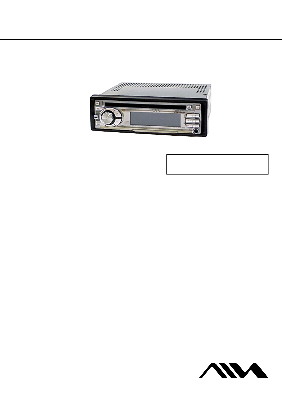
CDC-X237/X437
SERVICE MANUAL
Ver 1.0 2003. 01
• The tuner and CD sections have no adjustments.
SPECIFICATIONS
US Model
Canadian Model
CDC-X237/X437
AEP Model
UK Model
CDC-X237
Model Name Using Similar Mechanism NEW
CD Drive Mechanism Type MG-930A-185
Optical Pick-up Name OPTIMA-752B2
RADIO SECTION (US, Canadian model)
(FM)
Frequency Range: 87.5 MHz – 108 MHz
Usable Sensitivity: 12.7 dBf
50 dB Quieting Sensitivity: 17.2 dBf
IF Rejection: 100 dB
Frequency Response: 30 Hz – 15,000 Hz
S/N Ratio: 70 dB
Stereo Separation: 35 dB at 1 kHz
Alternate Channel Selectivity: 90 dB
Capture Ratio: 3 dB
(AM)
Frequency Range: 530 kHz – 1,710 kHz
Usable Sensitivity: 30 µV (30 dB)
RADIO SECTION (AEP, UK model)
(FM)
Frequency Range: 87.5 MHz – 108 MHz
Intermediate frequency: 10.7 MHz
Usable Sensitivity: 12.7 dBf
50 dB Quieting Sensitivity: 17.2 dBf
IF Rejection: 100 dB
Frequency Response: 30 Hz – 15,000 Hz
S/N Ratio: 67 dB
Stereo Separation: 35 dB at 1 kHz
Alternate Channel Selectivity: 90 dB
Capture Ratio: 3 dB
(MW)
Frequency Range: 531 kHz – 1,602 kHz
Intermediate frequency: 10.71 MHz/450 kHz
Usable Sensitivity: 30 µV (30 dB)
CD SECTION
Frequency Response: 17 Hz – 20 kHz +0/–3 dB
Dynamic Range: More than 85 dB
Channel Separation: More than 60 dB
S/N Ratio: More than 90 dB
Wow/Flutter: Unmeasurable
AUDIO SECTION
Max. Power Output: 45 W × 4 channels
AUX Input
Input sensitivity (load impedance) AUX: 300 mV (10 kΩ)
– Continued on next page –
FM/AM COMPACT DISC PLAYER
CDC-X237/X437
(LW)
Frequency Range: 144 kHz – 288 kHz (1-kHz/9-kHz steps)
Intermediate frequency: 10.71 MHz/450 kHz
Usable Sensitivity: 30 µV (30 dB)
9-877-001-01
2003A0400-1
© 2003. 01
Sony Corporation
e Vehicle Company
Published by Sony Engineering Corporation
FM/MW/LW COMPACT DISC PLAYER
CDC-X237
1
CDC-X237/X437
GENERAL
Power-Supply Voltage: 14.4 V (11 to 16 V allowable),
Load Impedance: 4 Ω
Tone Control: Bass ±10 dB at 100 Hz,
Preamp Output Voltage (load impedance): 2.2 V (10 kΩ)
Installed size: 182 (W) × 53 (H) × 155 (D) mm
Supplied Accessory: Carrying case (1)
CARD REMOTE CONTROL (CDC-X437)
Dimensions: approx. 33 (W) × 85 (H) × 7.5 (D) mm
Weight: approx. 20 g (0.7 oz.) (including battery)
• Specifications and external appearance are subject
to change without notice due to product improvement.
DC, negative ground
Treble ±10 dB at 10 kHz
(7 1/4 (W) × 2 1/8 (H) × 6 1/8 (D) inches)
(1 5/16 (W) × 3 3/8 (H) × 5/16 (D) inches)
SERVICE NOTES
NOTES ON HANDLING THE OPTICAL PICK-UP BLOCK
OR BASE UNIT
The laser diode in the optical pick-up block may suffer electrostatic
breakdown because of the potential difference generated by the
charged electrostatic load, etc. on clothing and the human body.
During repair, pay attention to electrostatic breakdown and also use
the procedure in the printed matter which is included in the repair
parts.
The flexible board is easily damaged and should be handled with
care.
NOTES ON LASER DIODE EMISSION CHECK
The laser beam on this model is concentrated so as to be focused on
the disc reflective surface by the objective lens in the optical pickup block. Therefore, when checking the laser diode emission, observe from more than 30 cm away from the objective lens.
Notes on Chip Component Replacement
• Never reuse a disconnected chip component.
• Notice that the minus side of a tantalum capacitor may be dam-
aged by heat.
• US, Canadian model
CAUTION
Use of controls or adjustments or performance of procedures
other than those specified herein may result in hazardous
radiation exposure.
• AEP, UK model
CAUTION
Use of controls or adjustments or performance of procedures other
than those specified herein may result in hazardous radiation
exposure.
This compact disc player is classified as a CLASS 1 LASER
product. The CLASS 1 LASER PRODUCT label is located on the
exterior.
SAFETY-RELATED COMPONENT WARNING!!
COMPONENTS IDENTIFIED BY MARK 0 OR DOTTED LINE
WITH MARK 0 ON THE SCHEMATIC DIAGRAMS AND IN
THE PARTS LIST ARE CRITICAL TO SAFE OPERATION.
REPLACE THESE COMPONENTS WITH SONY P ARTS WHOSE
PART NUMBERS APPEAR AS SHOWN IN THIS MANUAL OR
IN SUPPLEMENTS PUBLISHED BY SONY.
2
ATTENTION AU COMPOSANT AYANT RAPPORT
À LA SÉCURITÉ!!
LES COMPOSANTS IDENTIFIÉS P AR UNE MARQUE 0 SUR LES
DIAGRAMMES SCHÉMATIQUES ET LA LISTE DES PIÈCES
SONT CRITIQUES POUR LA SÉCURITÉ DE FONCTIONNEMENT.
NE REMPLACER CES COMPOSANTS QUE PAR DES PIÈCES
SONY DONT LES NUMÉROS SONT DONNÉS DANS CE MANUEL
OU DANS LES SUPPLÉMENTS PUBLIÉS PAR SONY.

TABLE OF CONTENTS
1. GENERAL
Connections ............................................................................. 4
2. DISASSEMBLY
2-1. Sub Panel Assy .................................................................... 6
2-2. CD Mechanism Block .........................................................6
2-3. Main Board Section ............................................................ 7
2-4. Main Board ......................................................................... 7
2-5. Heat Sink (CT) .................................................................... 8
2-6. Sub Board............................................................................ 8
2-7. Servo Board......................................................................... 9
2-8. Floating Block Assy ............................................................9
2-9. Lever Assy (CD Up Holder) ..............................................10
2-10. Lever (CD Roller) Sub Assy ............................................. 10
2-11. Lever Assy (CD Holder) ................................................... 11
2-12. Motor (Sled) Sub Assy...................................................... 11
2-13. Pick-up Sub Assy .............................................................. 12
3. DIAGRAMS
3-1. IC Pin Descriptions ........................................................... 13
3-2. Block Diagram –CD Section–........................................... 17
3-3. Block Diagram –Main Section–........................................ 18
3-4. Block Diagram –Front Section–........................................ 19
3-5. Circuit Boards Location .................................................... 19
3-6. Printed Wiring Boards –CD Mechanism Section–............ 20
3-7. Schematic Diagram –CD Mechanism Section– ................22
3-8. Printed Wiring Board –Main Section– .............................. 23
3-9. Schematic Diagram –Main Section (1/2)– ........................24
3-10. Schematic Diagram –Main Section (2/2)– ........................25
3-11. Printed Wiring Boards –Front Section– ............................ 26
3-12. Schematic Diagram –Front Section– ................................ 27
3-13. IC Block Diagrams............................................................ 28
CDC-X237/X437
4. EXPLODED VIEWS
4-1. Chassis Section ................................................................. 30
4-2. Front panel Section ........................................................... 31
4-3. CD Mechanism Section (1) ...............................................32
4-4. CD Mechanism Section (2) ...............................................33
5. ELECTRICAL PARTS LIST ........................................ 34
3
CDC-X237/X437
SECTION 1
GENERAL
This section is extracted
from instruction manual.
4
SECTION 2
DISASSEMBLY
Note : This set can be disassemble according to the following sequence.
SET
2-1. SUB PANEL ASSY
(Page 6)
2-2. CD MECHANISM BLOCK
(Page 6)
CDC-X237/X437
2-3. MAIN BOARD SECTION
(Page 7)
2-4. MAIN BOARD
(Page 7)
2-5. HEAT SINK (CT)
(Page 8)
2-6. SUB BOARD
(Page 8)
2-7. SERVO BOARD
(Page 9)
2-8. FLOATING BLOCK ASSY
(Page 9)
2-9. LEVER ASSY (CD UP HOLDER)
(Page 10)
2-10. LEVER (CD ROLLER) SUB ASSY
(Page 10)
2-13. PICK-UP SUB ASSY
(Page 12)
2-11. LEVER ASSY (CD HOLDER)
(Page 11)
2-12. MOTOR (SLED) SUB ASSY
(Page 11)
5
CDC-X237/X437
)
Note : Follow the disassembly procedure in the numerical order given.
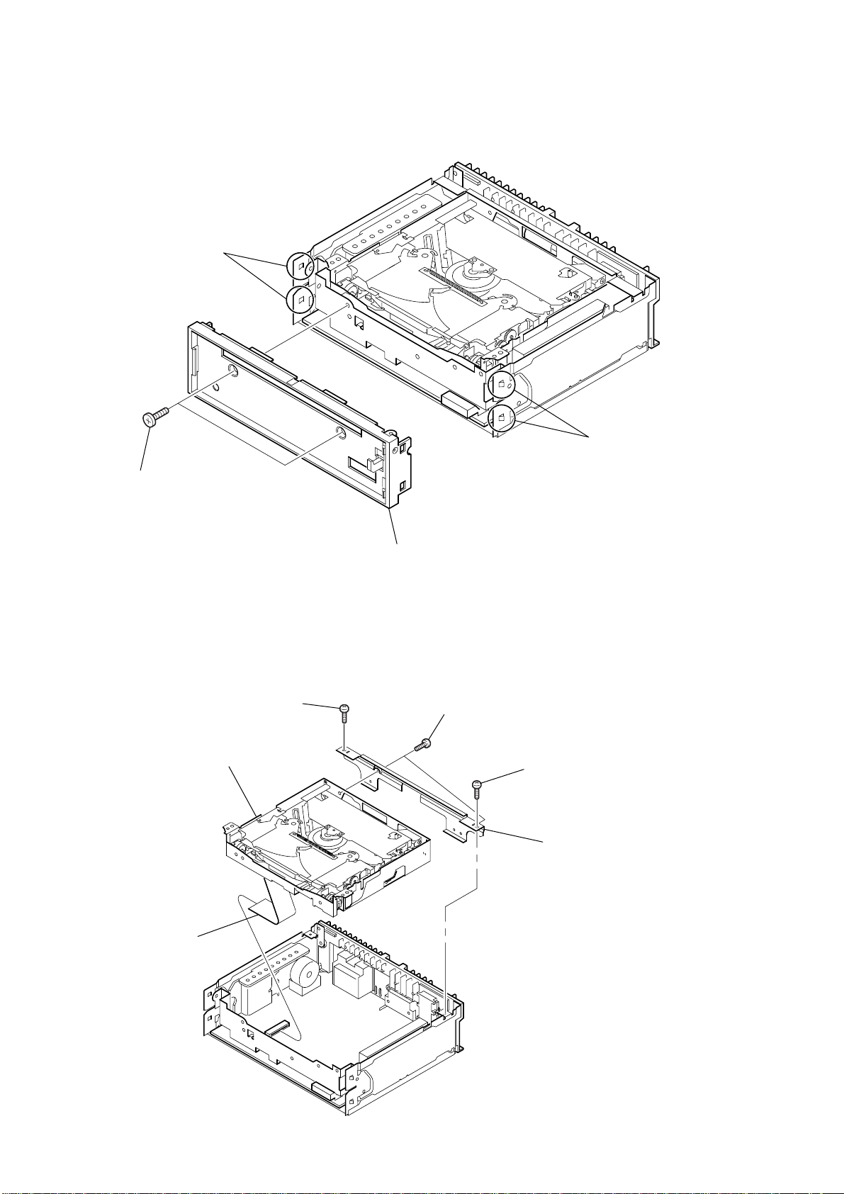
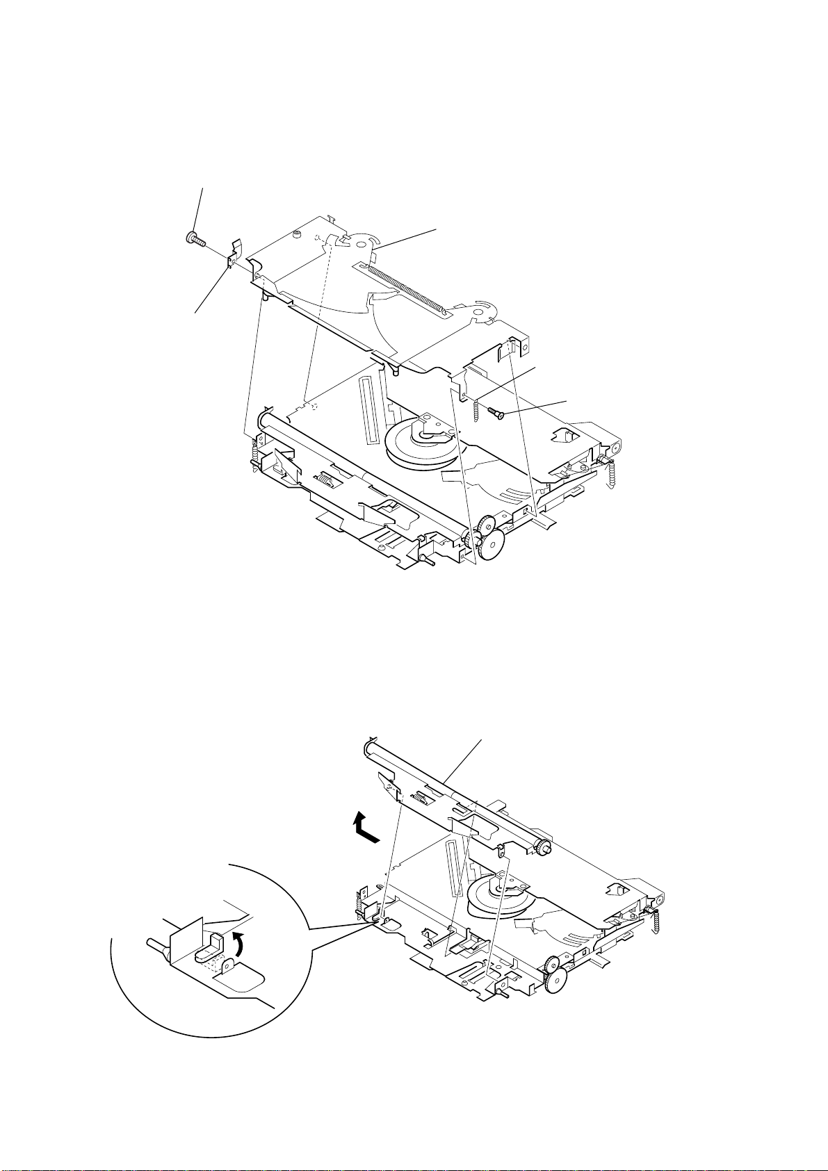
2-1. SUB PANEL ASSY
3
claws
2
claws
1
B 2.6x6
2-2. CD MECHANISM BLOCK
6
CD mechanism block
2
PTT 2.6x6
4
sub panel assy
4
P 2.6x4
1
PTT 2.6x6
5
holder (CD mecha
3
CON701
6
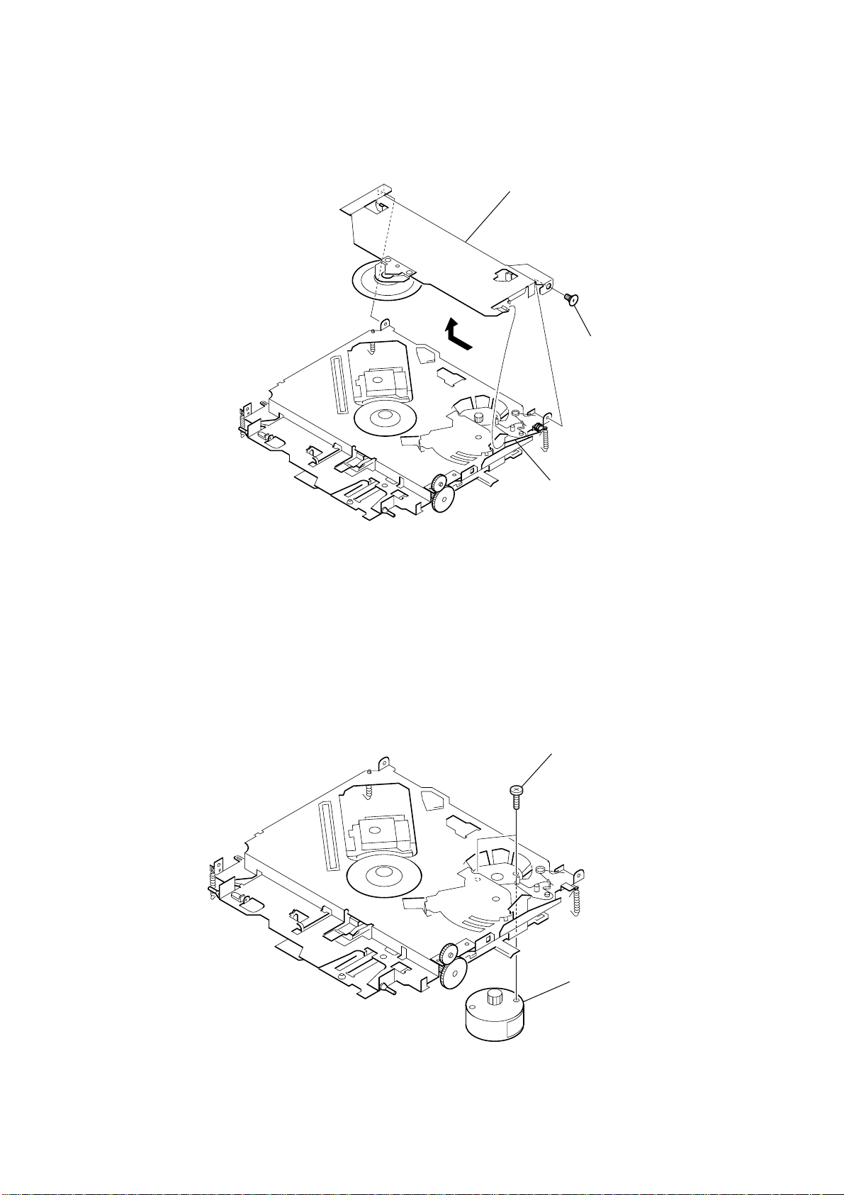
2-3. MAIN BOARD SECTION
6
6
Removal the solder.
7
MAIN board section
4
Removal the solder.
5
Removal the solder.
CDC-X237/X437
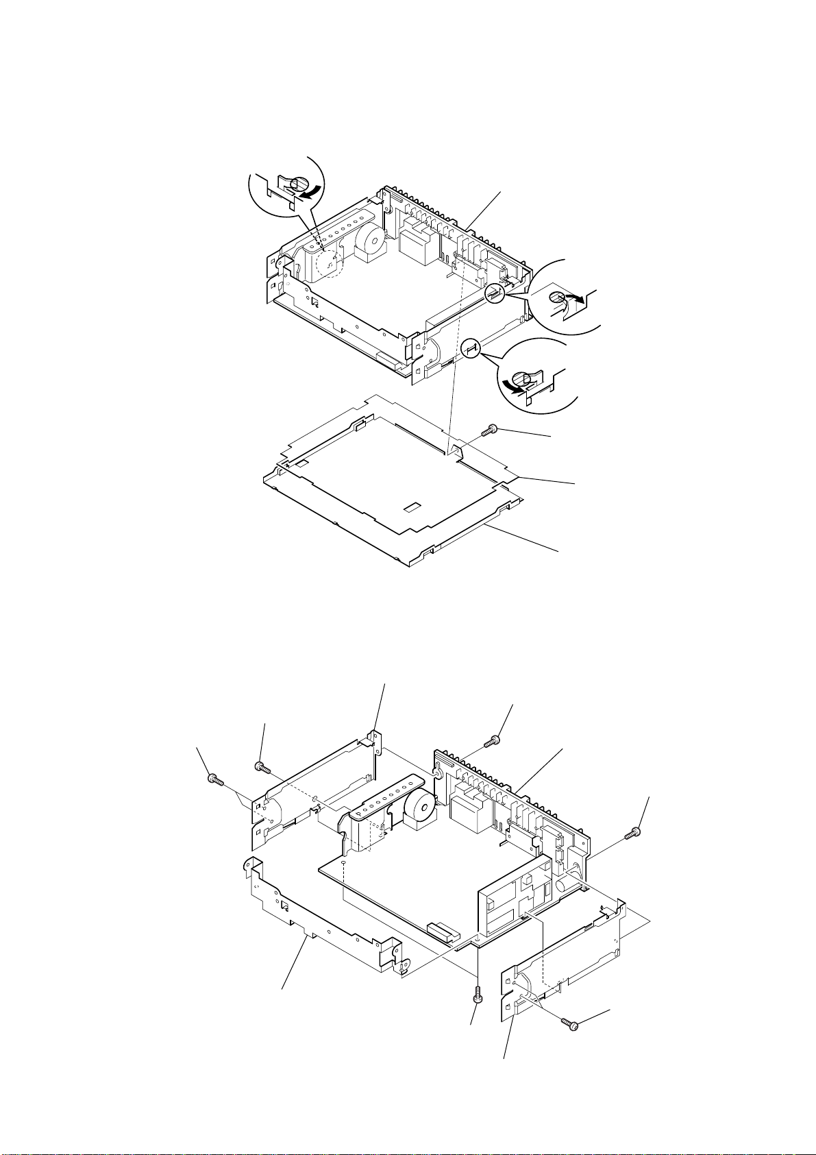
2-4. MAIN BOARD
5
PTT 2.6x6
4
PTT 2.6x6
6
side chassis (L)
1
PTT 2.6x6
1
PTP 2.6x4
3
2
cover
0
MAIN board
insulation sheet
2
PTT 2.6x
9
front chassis
3
PTT 2.6x6
8
side chassis (R)
7
PTT 2.6x6
7
CDC-X237/X437
8
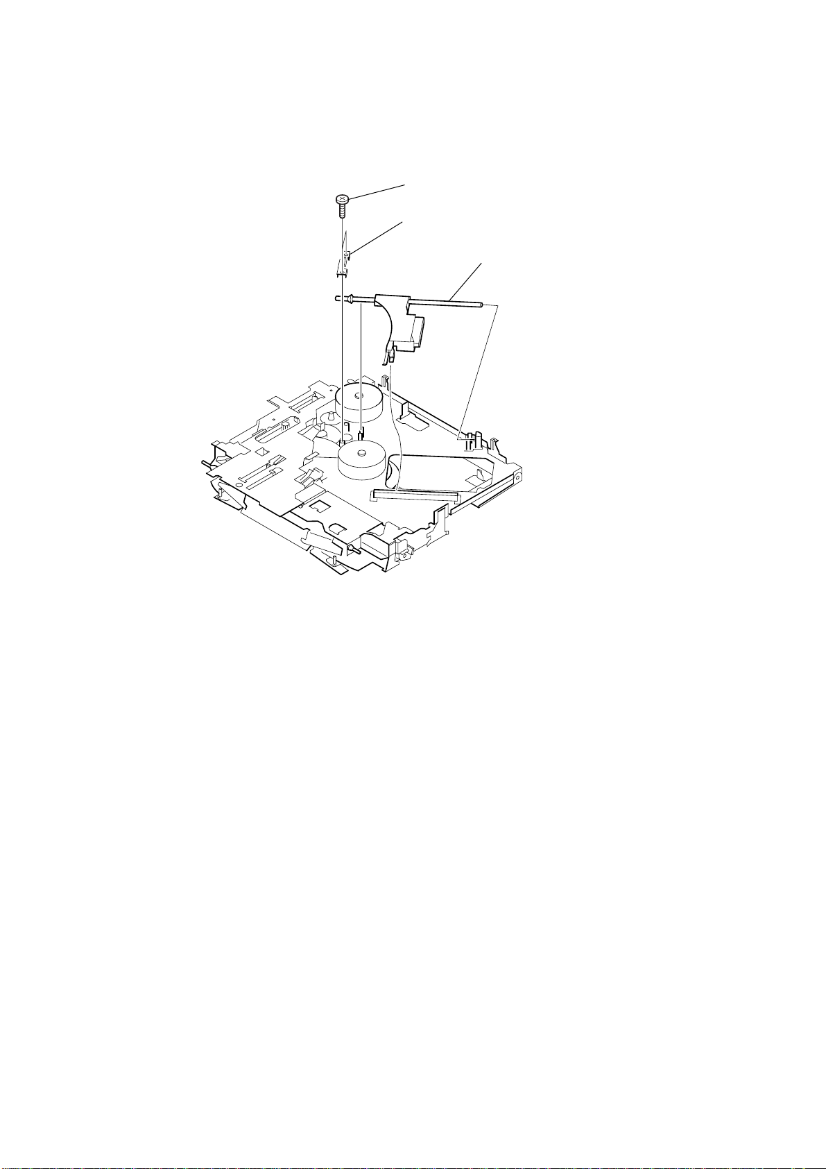
2-5. HEAT SINK (CT)
1
screw (2.6x8)
2
P 3x12
3
4
heat sink (CT)
PTT 2.6x
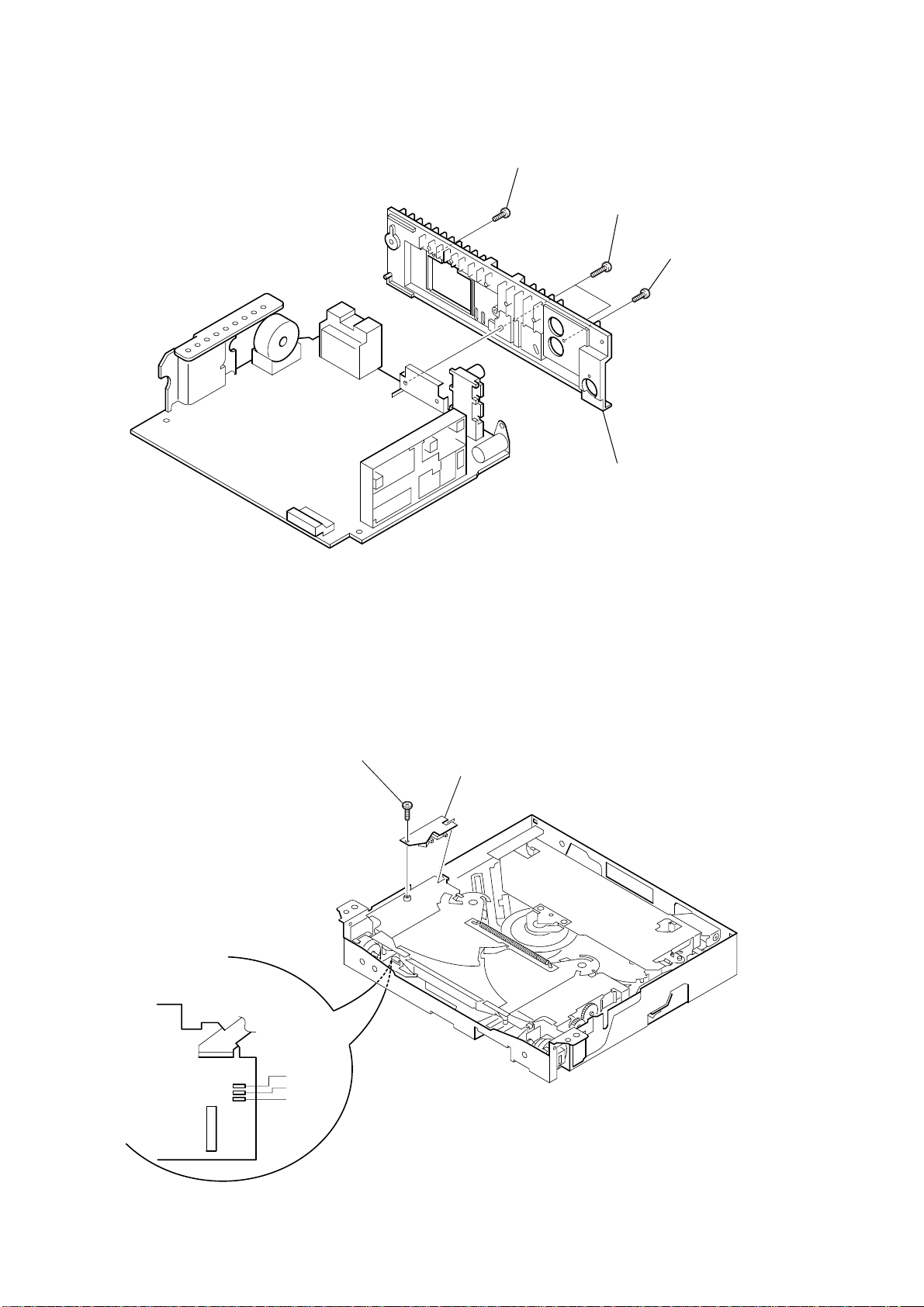
2-6. SUB BOARD
1
Removal the solders.
blue
brown
black
2
P 1.4x2
3
SUB board
8
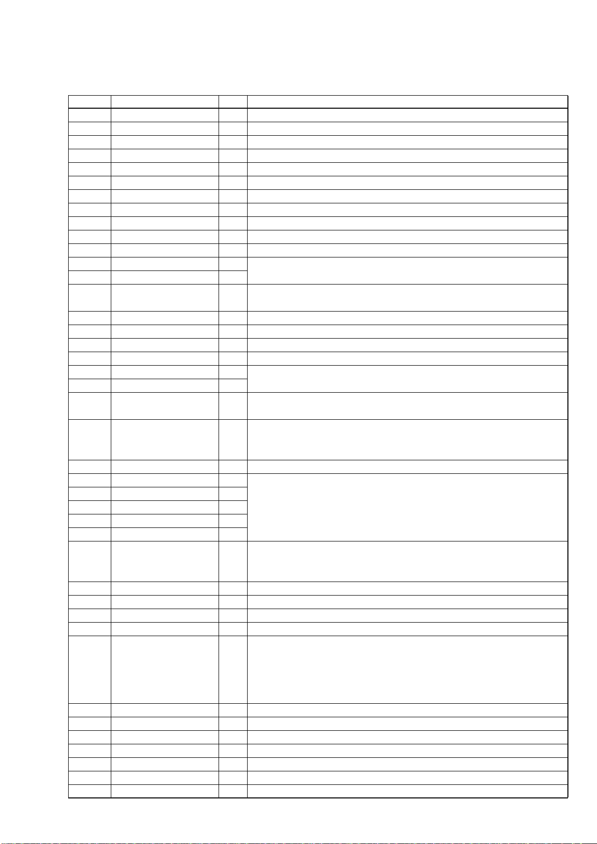
2-7. SERVO BOARD
2
PIC2 FLEXIBLE board
1
Removal the solders.
orange
blue
black
red
gry
CDC-X237/X437
white
3
PTT 2x3
2-8. FLOATING BLOCK ASSY
1
8
claw
qs
oil-damper
tension spring
0
5
SERVO board
4
screws (M1.7x4)
2
tension spring
qd
floating block aasy
3
tension spring
9
4
tension spring
7
claw
qa
5
tension spring
oil-damper
6
claw
9
CDC-X237/X437
w
2-9. LEVER ASSY (CD UP HOLDER)
1
P 1.4x2
2
leaf spring (roller)
5
lever assy (CD up holder)
4
tension spring
3
special scre
2-10. LEVER (CD ROLLER) SUB ASSY
1
2
3
lever (CD roller) sub assy
10
2-11. LEVER ASSY (CD HOLDER)
y
3
4
lever assy (CD holder)
2
special screw
CDC-X237/X437
2-12. MOTOR (SLED) SUB ASSY
1
torsion spring
1
P 1.7x2
2
motor (sled) sub ass
11
CDC-X237/X437
y
2-13. PICK-UP SUB ASSY
1
B 1.4x5
2
leaf spring
3
pick-up sub ass
12
CDC-X237/X437
SECTION 3
DIAGRAMS
3-1. IC PIN DESCRIPTIONS
• IC202 LC78622NE (DIGITAL SIGNAL PROCESSOR) (SERVO BOARD)
Pin No. Pin Name I/O Pin Description
1 DEFI I Defect detection signal (DEF) input (Must be connected to 0 V when unused.)
2TAI I Test input pin A pull-down resister is built-in. Must be connected to 0 V.
3 PDO O External VCO control phase comparator output
4 VVSS — Internal VCO ground pin Must be connected to 0 V.
5 ISET — PDO output current adjustment resister connection pin
6 VVDD — Internal VCO power supply pin
7FR—VCO frequency range adjustment
8 VSS — Digital system ground pin Must be connected to 0 V.
9 EFMO O EFM signal output
10 EFMIN I EFM signal input
11 TEST2 I Test input pin A pull-down resister is built-in. Must be connected to 0 V.
12 CLV+ O Disc motor control signal output
13 CLV– O Can be set to three-value output by microprocessor command.
14 V/P O
15 HFL I Track detection signal input This is a schmitt input.
16 TES I Tracking error signal input This is a schmitt input.
17 TOFF O Tracking off signal output
18 TGL O Tracking gain switching signal output Increase the gain when low.
19 JP+ O Track jump control signal output
20 JP– O Three-value output is also possible when specified by microprocessor command.
21 PCK O
22 FSEQ O Output a high level when the Synchronization signal detected from the EFM signal
23 VDD — Digital system power supply pin
24 CONT1 I/O General-purpose input/output 1 – 5
25 CONT2 I/O Controlled by serial data commands from the microprocessor.
26 CONT3 I/O Any of these that are unused must be either set up as input pin ports and connected to
27 CONT4 I/O 0 V, or set up as output pin ports and left open.
28 CONT5 I/O Not used. (Open)
29 EMPH O A high level indicates playback of a de-emphasis disc.
30 C2F O C2 flag output pin Not used. (Open)
31 DOUT O Digital out signal output (EIJA format) Not used. (Open)
32 TEST3 I Test input pin A pull-down resister is built-in. Must be connected to 0 V.
33 TEST4 I Test input pin A pull-down resister is built-in. Must be connected to 0 V.
34 PCCL I similar to those of LC78622E.
35 LMUTE O Left channel mute signal output General-purpose input/output pin 7
36 LVDD — Left channel power supply pin
37 LOUT O Left channel output
38 LVSS — Left channel ground pin Must be connected to 0 V.
39 RVSS — Right channel ground pin Must be connected to 0 V.
40 ROUT O Right channel output
41 RVDD — Right channel power supply pin
Rough servo/phase control automatic switching monitor output
Outputs a high level during rough servo a low level.
EFM data playback clock monitor signal output
Output pin 4.3218 MHz when the phase is locked. Not used. (Open)
Synchronization signal detection signal output
and the internaly generated synchronization signal range. Not used. (Open)
De-emphasis monitor signal output
General-purpose input/output pin 6. Not used. (Open)
General-purpose input/output command identifying pin
A pull-down resister is built-in. Must be connected to 0 V when used with functions
H: Control possible only for the general-purpose input/output port command.
L: Control possible for all commands.
13
 Loading...