

Sony CDCR-504-MP Service manual
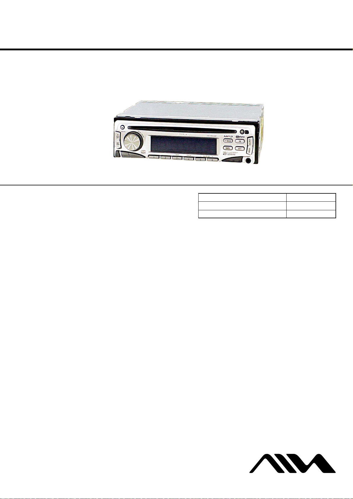
CDC-R504MP/X504MP
SERVICE MANUAL
Ver 1.0 2004. 01
Photo: CDC-X504MP
• The tuner and CD sections have no adjustments.
AUDIO POWER SPECIFICATIONS (US MODEL)
POWER OUTPUT AND TOTAL HARMONIC DISTORTION
23.2 watts per channel minimum continuous average power into
4 ohms, 4 channels driven from 20 Hz to 20 kHz with no more
than 5% total harmonic distortion.
SPECIFICATIONS
Tuner section
FM
Tuning range US, Canadian Model:
Antenna terminal External antenna connector
Intermediate frequency 10.7 MHz/450 kHz
Usable sensitivity 9 dBf
Selectivity 75 dB at 400 kHz
Signal-to-noise ratio 67 dB (stereo),
Harmonic distortion at 1 kHz
Separation 35 dB at 1 kHz
Frequency response 30 – 15,000 Hz
AM (US, Canadian Model)
Tuning range 530 – 1,710 kHz
Antenna terminal External antenna connector
Intermediate frequency 10.7 MHz/450 kHz
Sensitivity 30 µV
MW/LW (AEP, UK Model)
Tuning range MW: 531 – 1,602 kHz
Antenna terminal External antenna connector
Intermediate frequency 10.7 MHz/450 kHz
Sensitivity MW: 30 µV
CD player section
Signal-to-noise ratio 120 dB
Frequency response 10 – 20,000 Hz
Wow and flutter Below measurable limit
87.5 – 107.9 MHz
AEP, UK Model:
87.5 – 108 MHz
69 dB (mono)
0.5% (stereo),
0.3% (mono)
LW: 153 – 279 kHz
LW: 40 µV
FM/MW/LW COMPACT DISC PLAYER
US Model
Canadian Model
CDC-X504MP
AEP Model
UK Model
CDC-R504MP/X504MP
Model Name Using Similar Mechanism CDX-R3300/R3300T
CD Drive Mechanism Type MG-611MA-186//Q
Optical Pick-up Name KSS1000E
Power amplifier section
Outputs Speaker outputs
(sure seal connectors)
Speaker impedance 4 – 8 ohms
Maximum power output 52 W × 4 (at 4 ohms)
General
Outputs Audio outputs terminal (rear/sub switchable)
Power antenna relay control terminal
Power amplifier control terminal
Inputs Telephone ATT control terminal (AEP, UK Model)
Antenna input terminal
Tone controls Low: ±10 dB at 60 Hz (HIP-HOP)
Mid: ±10 dB at 1 kHz (HIP-HOP)
High: ±10 dB at 10 kHz (HIP-HOP)
Power requirements 12 V DC car battery (negative ground)
Dimensions Approx. 178 × 50 × 176 mm
(7 1/8 × 2 × 7 in.) (w/h/d)
Mounting dimensions Approx. 182 × 53 × 161 mm
(7 1/4 × 2 1/8 × 6 3/8 in.) (w/h/d)
Mass Approx. 1.2 kg (2 lb. 10 oz.)
Supplied accessories Parts for installation and connections (1 set)
Front panel case (1)
Card remote control RM-Z304
Design and specifications are subject to change without
notice.
FM/AM COMPACT DISC PLAYER
US, Canadian model
9-877-518-01
2004A04-1
© 2004. 01
AEP, UK model
Sony Corporation
e Vehicle Company
Published by Sony Engineering Corporation
1
CDC-R504MP/X504MP
SERVICE NOTES
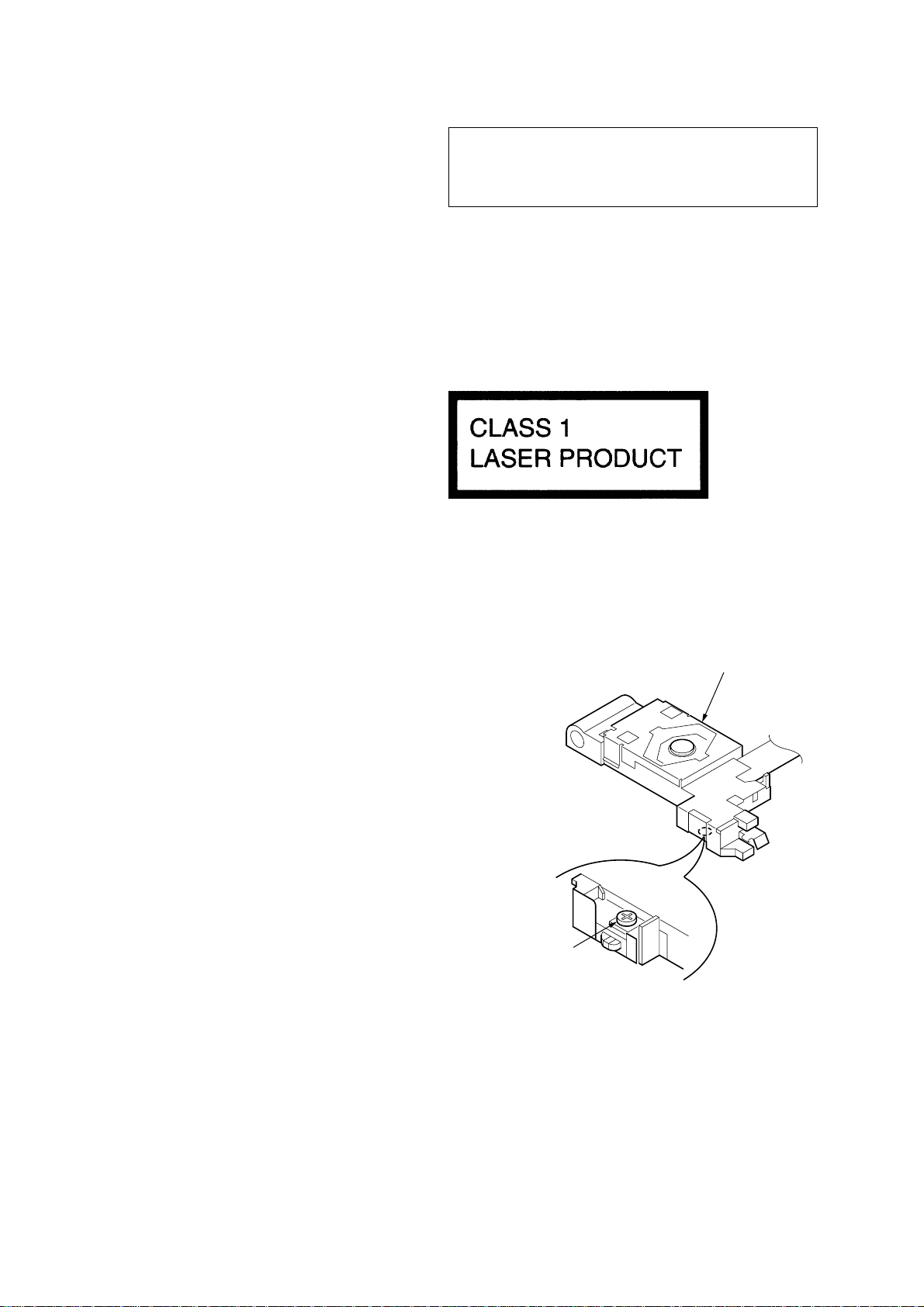
NOTES ON HANDLING THE OPTICAL PICK-UP BLOCK
OR BASE UNIT
The laser diode in the optical pick-up block may suffer electrostatic
breakdown because of the potential difference generated by the
charged electrostatic load, etc. on clothing and the human body.
During repair, pay attention to electrostatic breakdown and also use
the procedure in the printed matter which is included in the repair
parts.
The flexible board is easily damaged and should be handled with
care.
NOTES ON LASER DIODE EMISSION CHECK
The laser beam on this model is concentrated so as to be focused on
the disc reflective surface by the objective lens in the optical pickup block. Therefore, when checking the laser diode emission, observe from more than 30 cm away from the objective lens.
Notes on Chip Component Replacement
• Never reuse a disconnected chip component.
• Notice that the minus side of a tantalum capacitor may be dam-
aged by heat.
TEST DISCS
This set can playback CD-R and CD-ROM discs. The following
test discs should be used to check the capability:
CD-R test disc TCD-R082LMT (Part No. J-2502-063-1)
CD-RW test disc TCD-W082L (Part No. J-2502-063-2)
• US, Canadian model
CAUTION
Use of controls or adjustments or performance of procedures
other than those specified herein may result in hazardous
radiation exposure.
• AEP, UK model
CAUTION
Use of controls or adjustments or performance of procedures other
than those specified herein may result in hazardous radiation
exposure.
This compact disc player is classified as a CLASS 1 LASER
product. The CLASS 1 LASER PRODUCT label is located on the
exterior.
This label is located on the bottom of the chassis.
If the optical pick-up block is defective, please replace the whole
optical pick-up block.
Never turn the semi-fixed resistor located at the side of optical
pick-up block.
SAFETY-RELATED COMPONENT WARNING!!
optical pick-up
semi-fixed resistor
ATTENTION AU COMPOSANT AYANT RAPPORT
À LA SÉCURITÉ!!
COMPONENTS IDENTIFIED BY MARK 0 OR DOTTED LINE
WITH MARK 0 ON THE SCHEMATIC DIAGRAMS AND IN
THE PARTS LIST ARE CRITICAL TO SAFE OPERATION.
REPLACE THESE COMPONENTS WITH SONY P ARTS WHOSE
PART NUMBERS APPEAR AS SHOWN IN THIS MANUAL OR
IN SUPPLEMENTS PUBLISHED BY SONY.
2
LES COMPOSANTS IDENTIFIÉS P AR UNE MARQUE 0 SUR LES
DIAGRAMMES SCHÉMATIQUES ET LA LISTE DES PIÈCES
SONT CRITIQUES POUR LA SÉCURITÉ DE FONCTIONNEMENT.
NE REMPLACER CES COMPOSANTS QUE PAR DES PIÈCES
SONY DONT LES NUMÉROS SONT DONNÉS DANS CE MANUEL
OU DANS LES SUPPLÉMENTS PUBLIÉS PAR SONY.
CDC-R504MP/X504MP
D
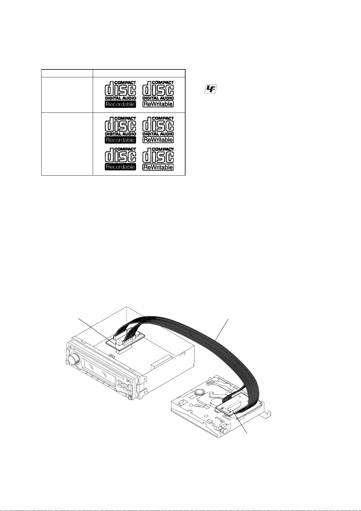
Notes on CD-Rs (recordable CDs)/CD-RWs (rewritable
CDs)
This unit can play the following discs:
Type of discs Label on the disc
Audio CD
MP3 files
• Some CD-Rs/CD-RWs (depending on the equipment used for
its recording or the condition of the disc) may not play on this
unit.
• You cannot play a CD-R/CD-RW that is not finalized∗.
• You can play MP3 files recorded on CD-ROMs, CD-Rs, and
CD-RWs.
• A CD-R/CD-RW to which a session can be added can be played.
z
UNLEADED SOLDER
Boards requiring use of unleaded solder are printed with the lead
free mark (LF) indicating the solder contains no lead.
(Caution: Some printed circuit boards may not come printed with
the lead free mark due to their particular size.)
: LEAD FREE MARK
Unleaded solder has the following characteristics.
• Unleaded solder melts at a temperature about 40°C higher than
ordinary solder.
Ordinary soldering irons can be used but the iron tip has to be
applied to the solder joint for a slightly longer time.
Soldering irons using a temperature regulator should be set to
about 350°C.
Caution: The printed pattern (copper foil) may peel away if the
heated tip is applied for too long, so be careful!
• Strong viscosity
Unleaded solder is more viscous (sticky, less prone to flow)
than ordinary solder so use caution not to let solder bridges
occur such as on IC pins, etc.
• Usable with ordinary solder
It is best to use only unleaded solder but unleaded solder may
also be added to ordinary solder.
∗ A process necessary for a recorded CD-R/CD-RW disc to be
played on the audio CD player.
EXTENSION CABLE AND SERVICE POSITION
When repairing or servicing this set, connect the jig (extension cable)
as shown below.
• Connect the MAIN board (CN301) and the SERVO board (CN2)
with the extension cable (Part No. J-2502-076-1).
MAIN BOARD
CN301
J-2502-076-1
SERVO BOAR
CN2
3

CDC-R504MP/X504MP
TABLE OF CONTENTS
1. GENERAL
Location of Controls................................................................ 5
Connections (US, Canadian Model)........................................ 6
Connections (AEP, UK Model) ............................................... 7
2. DISASSEMBLY
2-1. Sub Panel Assy.................................................................... 9
2-2. CD Mechanism Block ......................................................... 9
2-3. Main Board ....................................................................... 10
2-4. Chassis (T) Sub Assy ........................................................10
2-5. Roller Arm Assy ................................................................ 11
2-6. Chassis (OP) Assy............................................................. 11
2-7. Optical Pick-up ................................................................. 12
2-8. SL Motor Assy (M902) ..................................................... 12
2-9. LE Motor Assy (M903)..................................................... 13
2-10. Servo Board....................................................................... 13
3. DIAGRAMS
3-1. IC Pin Descriptions ...........................................................14
3-2. Block Diagram –CD Section–........................................... 19
3-3. Block Diagram –Main Section–........................................ 20
3-4. Block Diagram –Display Section–.................................... 21
3-5. Circuit Boards Location .................................................... 21
3-6. Note for Printed Wiring Boards and
Schematic Diagrams .......................................................... 22
3-7. Waveforms......................................................................... 22
3-8. Printed Wiring Boards –CD Mechanism Section–............ 23
3-9. Schematic Diagram –CD Mechanism Section (1/2)– ....... 24
3-10. Schematic Diagram –CD Mechanism Section (2/2)– ....... 25
3-11. Schematic Diagram –Main Section (1/2)– ........................ 26
3-12. Schematic Diagram –Main Section (2/2)– ........................ 27
3-13. Printed Wiring Board –Main Section– .............................. 28
3-14. Printed Wiring Boards –Display Section– ........................ 29
3-15. Schematic Diagram –Display Section–............................. 30
3-16. IC Block Diagrams............................................................ 31
4. EXPLODED VIEWS
4-1. Main Section ..................................................................... 35
4-2. Front Panel Section ...........................................................36
4-3. CD Mechanism Section (1) ............................................... 37
4-4. CD Mechanism Section (2) ............................................... 38
4-5. CD Mechanism Section (3) ............................................... 39
4-6. CD Mechanism Section (4) ............................................... 40
5. ELECTRICAL PARTS LIST ........................................41
4
LOCATION OF CONTROLS
SECTION 1
GENERAL
CDC-R504MP/X504MP
This section is extracted
from instruction manual.
5
CDC-R504MP/X504MP
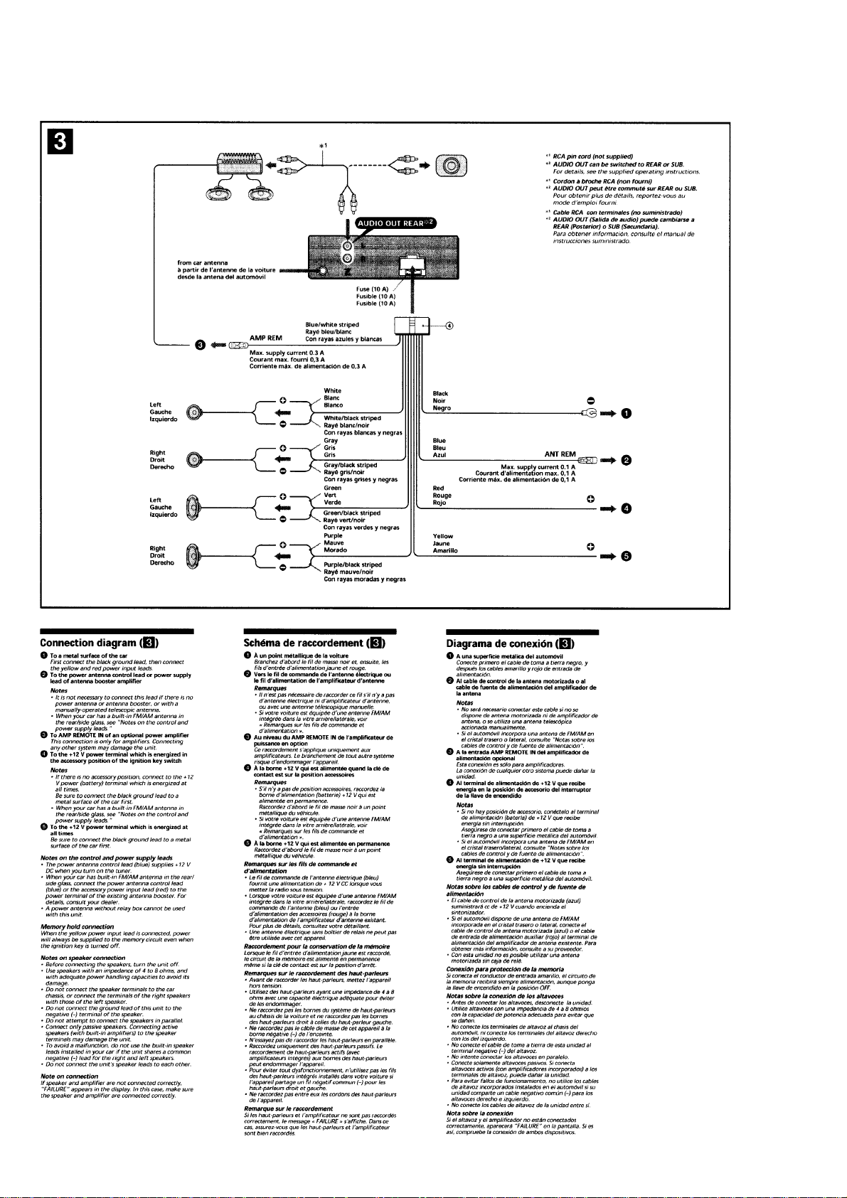
CONNECTIONS (US, Canadian Model)
6
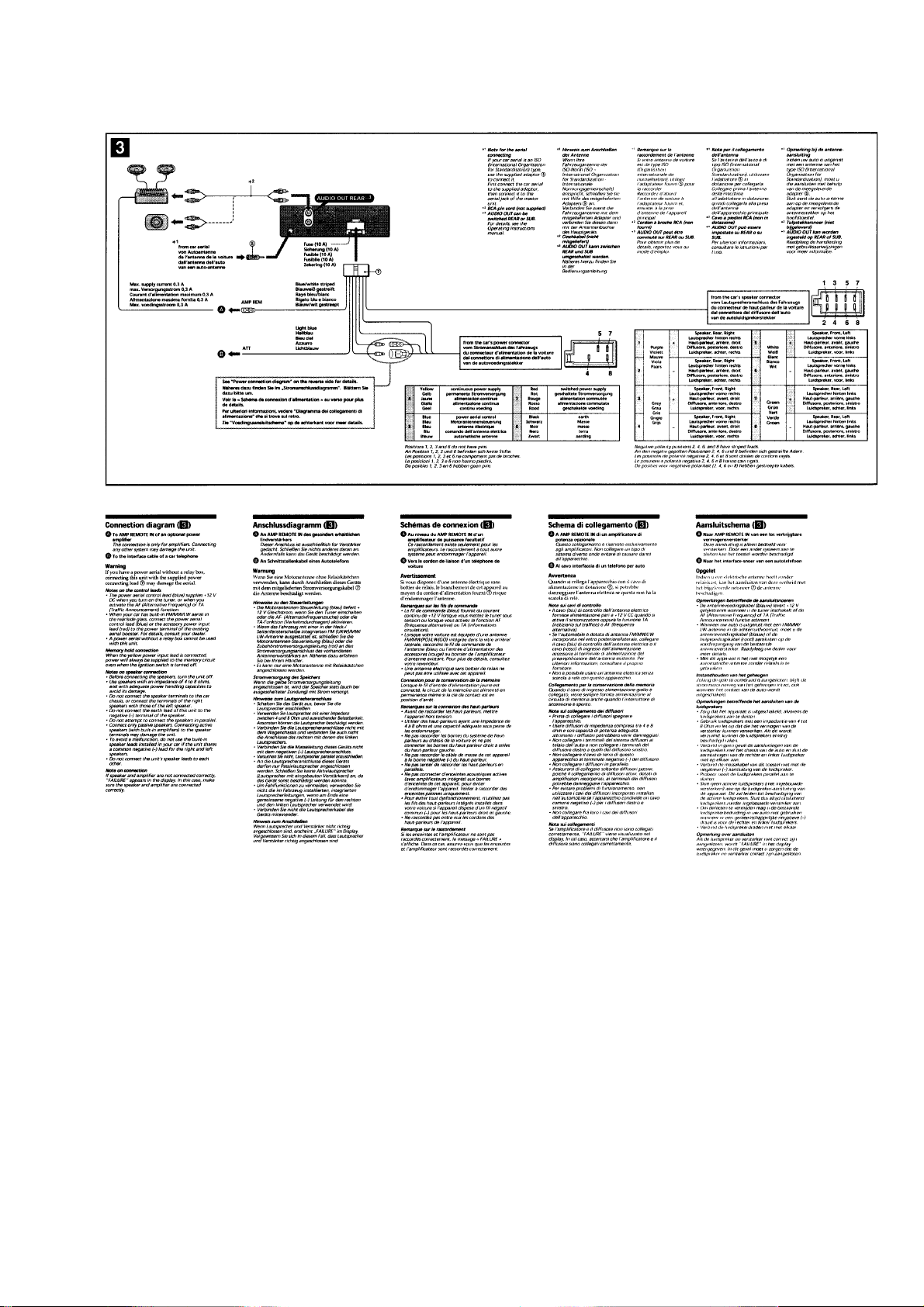
CONNECTIONS (AEP, UK Model)
CDC-R504MP/X504MP
7
CDC-R504MP/X504MP
SECTION 2
DISASSEMBLY
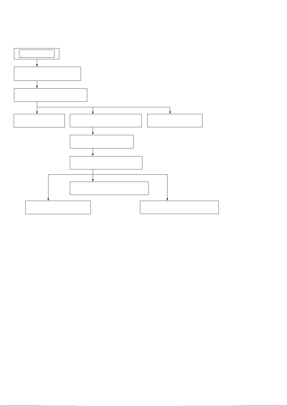
Note : This set can be disassemble according to the following sequence.
SET
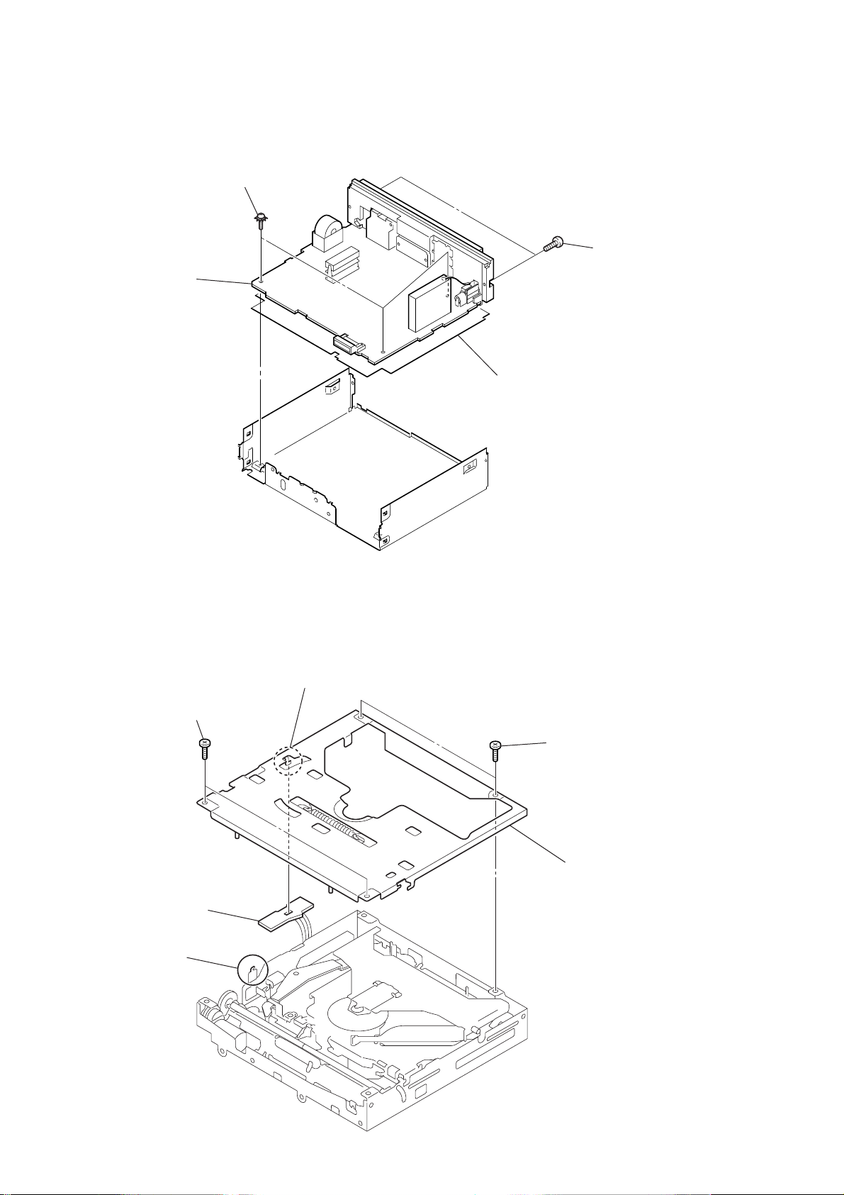
2-1. SUB PANEL ASSY
(Page 9)
2-2. CD MECHANISM BLOCK
(Page 9)
2-3. MAIN BOARD
(Page 10)
2-7. OPTICAL PICK-UP
(Page 12)
2-4. CHASSIS (T) SUB ASSY
(Page 10)
2-5. ROLLER ARM ASSY
(Page 11)
2-6. CHASSIS (OP) ASSY
(Page 11)
2-8. SL MOTOR ASSY (M902)
(Page 12)
2-10. SERVO BOARD
(Page 13)
2-9. LE MOTOR ASSY (M903)
(Page 13)
8
Note : Follow the disassembly procedure in the numerical order given.
s
)
2-1. SUB PANEL ASSY
3
two claws
CDC-R504MP/X504MP
1
two
screws
(+PTT 2.6
x
6)
2-2. CD MECHANISM BLOCK
5
CD mechanism block
4
sub panel assy
7
bracket (CD)
6
two
screws
(+PTT 2.6
2
two claw
x
4)
2
screw
(+PTT 2.6
x
6)
3
4
CN301
1
screw
(+PTT 2.6
x
6
9
CDC-R504MP/X504MP
)
2-3. MAIN BOARD
1
three ground point screws
(+PTT 2.6
3
MAIN board
x
6)
2
two
screws
x
(+PTT 2.6
insulating sheet
6
2-4. CHASSIS (T) SUB ASSY
2
two
screws
(+P 1.7
5
SENSOR board
3
claw
x
2.2)
4
claw
1
two
screws
x
(+P 1.7
6
2.2)
chassis (T) sub assy
10
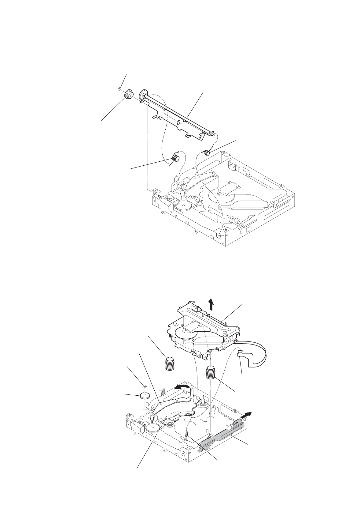
2-5. ROLLER ARM ASSY
4
worm wheel (RA)
1
spring (RAL)
3
washer (0.8-2.5)
5
roller arm assy
2
spring (RAR)
CDC-R504MP/X504MP
2-6. CHASSIS (OP) ASSY
0
coil spring (damper)
4
washer
5
gear (LE1)
lever (D)
6
8
qa
chassis (OP) assy
1
CN1
9
two coil springs (damper)
7
slider (R)
2
Remove the six solderings.
3
tension coil spring (KF)
11
CDC-R504MP/X504MP
)
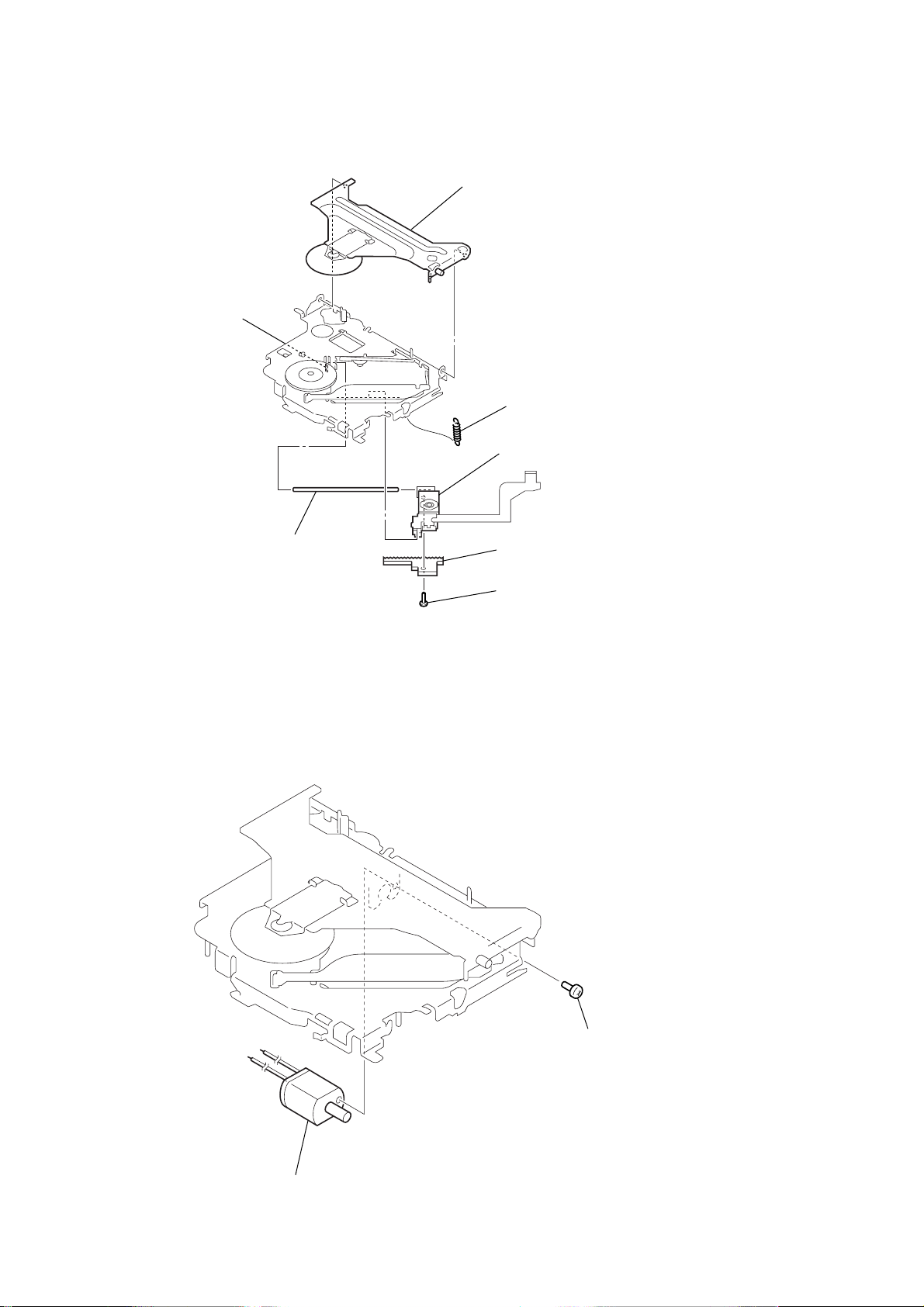
2-7. OPTICAL PICK-UP
5
claw
2
chucking arm sub assy
1
tension coil spring (CHKG
7
optical pick-up
2-8. SL MOTOR ASSY (M902)
6
main shaft
4
rack (SL)
3
screw
(+B 1.4
x
5)
12
2
SL motor assy (M902)
1
screw
(+P 1.4
x
1.8)
2-9. LE MOTOR ASSY (M903)
qf
two toothed lock
(+M 1.4
bracket (LEM)
qs
(+M 1.7
screw
x
)
screws
2.5)
6
screw
(+P 1.7
x
qd
2.2)
qa
screw
(+M 1.7
qg
(M903)
0
woam (LEB) assy
x
2.5)
LE motor assy
7
leaf spring (LE)
8
screw
(+M 1.7
9
bearing (LEB)
2
washer
gear (LE1)
3
lever (D)
x
CDC-R504MP/X504MP
2.5)
4
5
slider (R)
2-10. SERVO BOARD
1
Remove the eight solderings.
1
Remove the soldering.
6
SERVO board
2
Remove the three solderings.
4
toothed lock
(M 1.7)
5
screw
claw
3
CN1
13

CDC-R504MP/X504MP
SECTION 3
DIAGRAMS
3-1. IC PIN DESCRIPTIONS
• IC3 CXD3059AR (DIGIT AL SER VO/DIGITAL SIGNAL PROCESSOR) (SERVO BOARD (1/2))
Pin No. Pin Name I/O Pin Description
1MIRR I/O Mirrer signal input/output
2 DFCT I/O Defect signal input/output
3 FOK I/O Focus OK signal input/output
4 VSS — Ground pin
5 LOCK I/O Not used in this set. (Open)
6 MDP O Spindle motor servo control signal output
7 SSTP I Disc most inner detection signal input
8IOVSS1 — Digital ground pin for I/O
9 SFDR O Sled drive signal output
10 SRDR O Sled drive signal output
11 TFDR O Tracking drive signal output
12 TRDR O Tracking drive signal output
13 FFDR O Focus drive signal output
14 FRDR O Focus drive signal output
15 IOVDD1 — Digital power supply pin for I/O
16 AVDD0 — Analog power supply pin for I/O
17 AVSS0 — Analog ground pin
18 NC — Not used. (Open)
19 E I E signal input
20 F I F signal input
21 TEI I Tracking error signal input from the DSSP block
22 TEO O Tracking error signal output to the RF amp block
23 FEI I Focus error signal input from the DSSP block
24 FEO O Focus error signal output form the RF amp block
25 VC I/O
26 A I A signal input
27 B I B signal input
28 C I C signal input
29 D I D signal input
30 NC — Not used. (Open)
31 AVDD4 — Analog power supply pin
32 RFDCO I/O
33 PDSENS I Reference voltage input for PD
34 AC SUM O RFAC suming amp signal output
35 EQ IN I Equalizer circuit signal input
36 LD O APC amp signal output
37 PD I APC amp signal input
38 NC — Not used. (Open)
39 RFC I EQ cut off frequency adjustment input
40 AVSS4 — Analog ground pin
41 RFACO O RFAC signal output
42 RFACI I RFAC signal input or EFM signal input
43 AVDD3 — Analog power supply pin
44 BIAS I Asymmetry circuit constant current input
45 ASYI I Asymmetry comparate voltage input
46 ASYO O EFM full swing signal output
47 VPCO O Charge pomp output for wideband EFM PLL
48 VCTL I VCO2 control voltage input for wideband EFM PLL
49 AVSS3 — Analog ground pin
VC voltage output to the RF amp block
Center voltage input from the DSSP block by command select
RFDC signal output
RFDC signal input from the DSSP block by command select
14
CDC-R504MP/X504MP
Pin No. Pin Name I/O Pin Description
50 CLTV I VCO1 control voltage input
51 FILO O Filter signal output for master PLL
52 FILI I Filter signal input for master PLL
53 PCO O Charge pomp output for master PLL
54 AVDD5 — Analog power supply pin
55 DDVROUT O DC/DC converter output
56 DDVRSEN I DC/DC converter output voltage monitor signal input
57 AVSS5 — Analog ground pin
58 DDCR I Reset signal input for DC/DC converter
59 NC — Not used. (Open)
60 BCKI I D/A interface bit clock signal input
61 PCMDI I D/A interface serial data signal input
62 LRCKI I D/A interface LR clock signal input
63 LRCK O D/A interface LR clock signal output
64 VSS — Digital ground pin for internal
65 PCMD O D/A interface serial data signal output
66 BCK O D/A interface bit clock signal output
67 VDD — Digital power supply pin for internal
68 EMPH O Not used in this set. (Open)
69 EMPHI I Not used in this set. (Fixed at “L”.)
70 IOVDD2 — Digital power supply pin for I/O
71 DOUT O Digital out signal output
72, 73 TEST I Test pin Normally “L”.
74 IOVSS2 — Digital ground pin for I/O
75 NC — Not used in this set. (Open)
76 XVSS — Ground pin for master clock
77 XTAO O Crystal oscillation circuit output (16.9344 MHz)
78 XTAI I Crystal oscillation circuit input (16.9344 MHz)
79 XVDD — Power supply pin for master clock
80 AVDD1 — Analog power supply pin
81 AOUT1 O L channel analog signal output
82 VREFL O L channel reference voltage output
83 AVSS1 — Analog ground pin
84 AVSS2 — Analog ground pin
85 VREFR O R channel reference voltage output
86 AOUT2 O R channel analog signal output
87 AVDD2 — Analog power supply pin
88 NC — Not used. (Open)
89 IOVDD0 — Digital power supply pin for I/O
90 RMUT O R channel “O” detection flug output
91 LMUT O L channel “O” detection flug output
92 NC — Not used. (Open)
93 XTSL I X’tal select signal input 16.9344 MHz: “L”, 33.8688 MHz: “H”
94 IOVSS0 — Digital ground pin for I/O
95 XTACN I Oscillation circuit control input “H”: Oscillation start, “L”: Oscillation stop
96 SQSO O Sub 80 bit and PCM peak, level data signal output CD text data signal output
97 SQCK I Clock signal input for SQSO read out
98 SBSO O Sub P-W serial data signal output Not used in this set. (Open)
99 EXCK I Clock signal input for SBSO read out Not used in this set. (Open)
100 XRST I System reset signal input “L”: reset
101 SYSM I Mute signal input “H”: mute Not used in this set. (Fixed at “L”.)
102 DATA I Serial data signal input
103 VSS — Digital ground pin for internal
15
 Loading...