

Sony CDCR-30-MP Service manual
CDC-R30MP/X30MP
SERVICE MANUAL
Ver 1.1 2003. 08
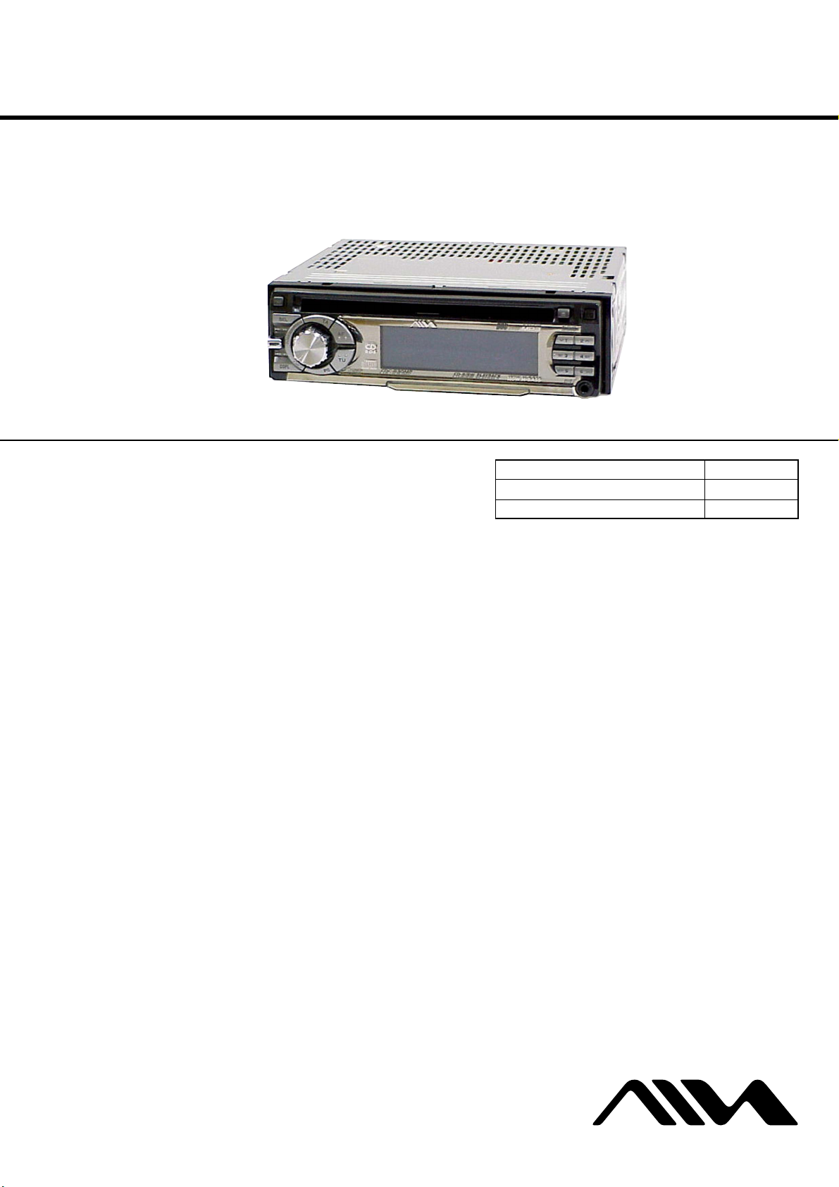
Photo: CDC-R30MP
• The CD section have no adjustment.
SPECIFICATIONS
US Model
Canadian Model
CDC-X30MP
AEP Model
UK Model
CDC-R30MP
Model Name Using Similar Mechanism NEW
CD Drive Mechanism Type MG-930M-185
Optical Pick-up Name OPTIMA-752B2
RADIO SECTION
(FM)
Frequency Range: 87.5 MHz – 108 MHz
Intermediate frequency: 10.7 MHz (CDC-R30MP)
Usable Sensitivity: 12.7 dBf
50 dB Quieting Sensitivity: 17.2 dBf
IF Rejection: 100 dB
Frequency Response: 30 Hz – 15,000 Hz
S/N Ratio: 67 dB (CDC-R30MP)
70 dB (CDC-X30MP)
Stereo Separation: 35 dB at 1 kHz
Alternate Channel Selectivity: 98 dB
Capture Ratio: 3 dB
(AM) (CDC-X30MP)
Frequency Range: 530 kHz – 1,710 kHz
Usable Sensitivity: 30 µV (30 dB)
(MW) (CDC-R30MP)
Frequency Range: 531 kHz – 1,602 kHz
Intermediate frequency: 10.71 MHz/450 kHz
Usable Sensitivity: 30 µV (30 dB)
(LW) (CDC-R30MP)
Frequency Range: 144 kHz – 288 kHz (1 kHz/9 kHz step)
Intermediate frequency: 10.71 MHz/450 kHz
Usable Sensitivity: 30 µV (30 dB)
CD SECTION
Frequency Response: 17 Hz – 20 kHz +0/–3 dB
Dynamic Range: More than 92 dB
Channel Separation: More than 60 dB
S/N Ratio: More than 90 dB
Wow/Flutter: Unmeasurable
MP3 Decoding: MPEG 1 Audio Layer 3
AUDIO SECTION
Max. Power Output: 45 W × 4 channels
AUX Input
Input sensitivity (load impedance) AUX: 300 mV (10 kΩ)
– Continued on next page –
FM/AM COMPACT DISC PLAYER
CDC-X30MP
9-877-187-02
2003H04-1
© 2003. 08
FM/MW/LW COMPACT DISC PLAYER
CDC-R30MP
Sony Corporation
e Vehicle Company
Published by Sony Engineering Corporation
1
CDC-R30MP/X30MP
GENERAL
Power-Supply Voltage: 14.4 V (11 to 16 V allowable),
Load Impedance: 4 Ω
Tone Control: Bass ±10 dB at 100 Hz,
Preamp Output Voltage (load impedance): 2.2 V (10 kΩ)
Installed size: 182 (W) × 53 (H) × 155 (D) mm
Supplied Accessory: Carrying case (1)
CARD REMOTE CONTROL
Dimensions: Approx. 33 (W) × 85 (H) × 7.5 (D) mm
Weight: Approx. 20 g (0.7 oz.) (including battery)
• Specifications and external appearance are subject
to change without notice due to product improvement.
DC, negative ground
Treble ±10 dB at 10 kHz
(7 1/4 (W) × 2 1/8 (H) × 6 1/8 (D) inches)
(1 5/16 (W) × 3 3/8 (H) × 5/16 (D) inches)
SERVICE NOTES
NOTES ON HANDLING THE OPTICAL PICK-UP BLOCK
OR BASE UNIT
The laser diode in the optical pick-up block may suffer electrostatic
breakdown because of the potential difference generated by the
charged electrostatic load, etc. on clothing and the human body.
During repair, pay attention to electrostatic breakdown and also use
the procedure in the printed matter which is included in the repair
parts.
The flexible board is easily damaged and should be handled with
care.
NOTES ON LASER DIODE EMISSION CHECK
The laser beam on this model is concentrated so as to be focused on
the disc reflective surface by the objective lens in the optical pickup block. Therefore, when checking the laser diode emission, observe from more than 30 cm away from the objective lens.
Notes on Chip Component Replacement
• Never reuse a disconnected chip component.
• Notice that the minus side of a tantalum capacitor may be dam-
aged by heat.
CDC-X30MP:
CAUTION
Use of controls or adjustments or performance of procedures
other than those specified herein may result in hazardous
radiation exposure.
CDC-R30MP:
CAUTION
Use of controls or adjustments or performance of procedures other
than those specified herein may result in hazardous radiation
exposure.
This compact disc player is classified as a CLASS 1 LASER
product. The CLASS 1 LASER PRODUCT label is located on the
exterior.
SAFETY-RELATED COMPONENT WARNING!!
COMPONENTS IDENTIFIED BY MARK 0 OR DOTTED LINE
WITH MARK 0 ON THE SCHEMATIC DIAGRAMS AND IN
THE PARTS LIST ARE CRITICAL TO SAFE OPERATION.
REPLACE THESE COMPONENTS WITH SONY P ARTS WHOSE
PART NUMBERS APPEAR AS SHOWN IN THIS MANUAL OR
IN SUPPLEMENTS PUBLISHED BY SONY.
2
ATTENTION AU COMPOSANT AYANT RAPPORT
À LA SÉCURITÉ!!
LES COMPOSANTS IDENTIFIÉS P AR UNE MARQUE 0 SUR LES
DIAGRAMMES SCHÉMATIQUES ET LA LISTE DES PIÈCES
SONT CRITIQUES POUR LA SÉCURITÉ DE FONCTIONNEMENT.
NE REMPLACER CES COMPOSANTS QUE PAR DES PIÈCES
SONY DONT LES NUMÉROS SONT DONNÉS DANS CE MANUEL
OU DANS LES SUPPLÉMENTS PUBLIÉS PAR SONY.

TABLE OF CONTENTS
1. GENERAL
Connections (CDC-X30MP) ...................................................4
Connections (CDC-R30MP) ................................................... 5
2. DISASSEMBLY
2-1. Sub Panel Assy .................................................................... 8
2-2. CD Mechanism Block ......................................................... 8
2-3. Main Board Section ............................................................ 9
2-4. Main Board ......................................................................... 9
2-5. Heat Sink (CT) .................................................................. 10
2-6. Sub Board.......................................................................... 10
2-7. Servo Board....................................................................... 11
2-8. Floating Block Assy .......................................................... 11
2-9. Lever Assy (CD Up Holder CNF) ..................................... 12
2-10. Lever (CD Roller) Sub Assy ............................................. 12
2-11. Lever Assy (CD Holder) ................................................... 13
2-12. Motor (Sled) Sub Assy...................................................... 13
2-13. Pick-up Sub Assy .............................................................. 14
3. ELECTRICAL ADJUSTMENT.................................... 15
CDC-R30MP/X30MP
4. DIAGRAMS
4-1. IC Pin Descriptions ........................................................... 16
4-2. Block Diagram –CD Section–........................................... 23
4-3. Block Diagram –Main Section–........................................ 24
4-4. Block Diagram –Front Section–........................................ 25
4-5. Circuit Boards Location .................................................... 25
4-6. Printed Wiring Boards –CD Mechanism Section–............ 26
4-7. Schematic Diagram –CD Mechanism Section (1/2)– ....... 28
4-8. Schematic Diagram –CD Mechanism Section (2/2)– ....... 29
4-9. Printed Wiring Board –Main Section– .............................. 30
4-10. Schematic Diagram –Main Section (1/2)– ........................ 31
4-11. Schematic Diagram –Main Section (2/2)– ........................ 32
4-12. Printed Wiring Boards –Front Section– ............................ 33
4-13. Schematic Diagram –Front Section– ................................ 34
4-14. IC Block Diagrams............................................................ 35
5. EXPLODED VIEWS
5-1. Chassis Section ................................................................. 38
5-2. Front panel Section ........................................................... 39
5-3. CD Mechanism Section (1) ............................................... 40
5-4. CD Mechanism Section (2) ............................................... 41
6. ELECTRICAL PARTS LIST ........................................ 42
3
CDC-R30MP/X30MP
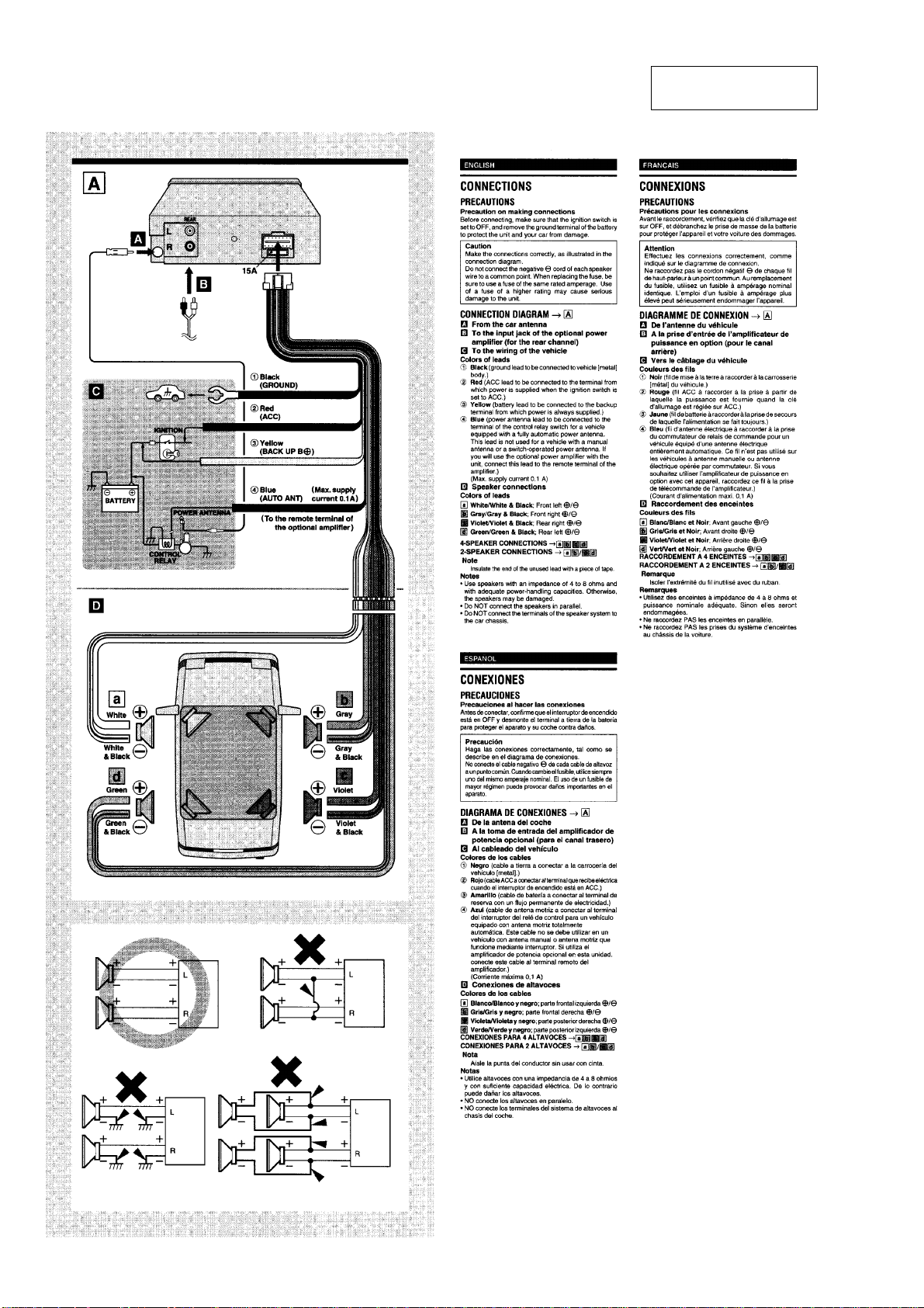
CONNECTIONS (CDC-X30MP)
SECTION 1
GENERAL
This section is extracted
from instruction manual.
4
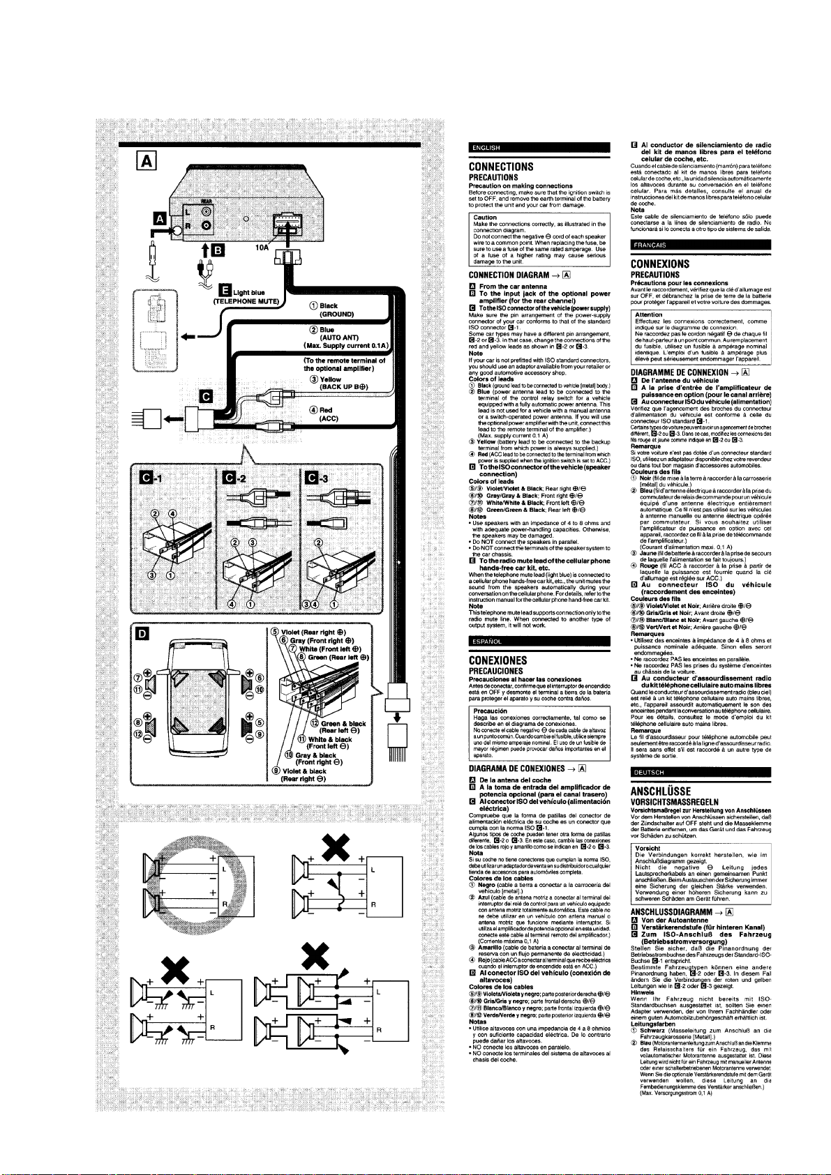
CONNECTIONS (CDC-R30MP)
CDC-R30MP/X30MP
5
CDC-R30MP/X30MP
6
SECTION 2
DISASSEMBLY
Note : This set can be disassemble according to the following sequence.
SET
2-1. SUB PANEL ASSY
(Page 8)
2-2. CD MECHANISM BLOCK
(Page 8)
CDC-R30MP/X30MP
2-3. MAIN BOARD SECTION
(Page 9)
2-4. MAIN BOARD
(Page 9)
2-5. HEAT SINK (CT)
(Page 10)
2-6. SUB BOARD
(Page 10)
2-7. SERVO BOARD
(Page 11)
2-8. FLOATING BLOCK ASSY
(Page 11)
2-9. LEVER ASSY (CD UP HOLDER CNF)
(Page 12)
2-10. LEVER (CD ROLLER) SUB SSY
(Page 12)
2-13. PICK-UP SUB ASSY
(Page 14)
2-11. LEVER ASSY (CD HOLDER)
(Page 13)
2-12. MOTOR (SLED) SUB ASSY
(Page 13)
7
CDC-R30MP/X30MP
)
Note : Follow the disassembly procedure in the numerical order given.
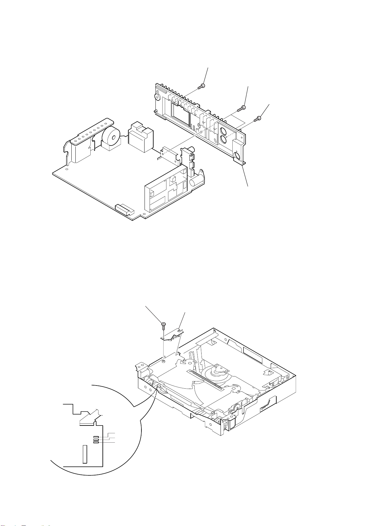
2-1. SUB PANEL ASSY
3
claws
2
claws
1
B 2.6x6
2-2. CD MECHANISM BLOCK
6
CD mechanism block
2
PTT 2.6x6
4
sub panel assy
4
P 2.6x4
1
PTT 2.6x6
5
holder (CD mecha
3
CON701
8
2-3. MAIN BOARD SECTION
6
6
Removal the solder.
7
MAIN board section
4
Removal the solder.
5
Removal the solder.
CDC-R30MP/X30MP
2-4. MAIN BOARD
5
PTT 2.6x6
4
PTT 2.6x6
6
side chassis (L)
1
PTT 2.6x6
1
PTP 2.6x4
3
2
cover
0
MAIN board
insulation sheet
2
PTT 2.6x
9
front chassis
3
PTT 2.6x6
8
side chassis (R)
7
PTT 2.6x6
9
CDC-R30MP/X30MP
8
2-5. HEAT SINK (CT)
1
screw (2.6x8)
2
P 3x12
3
4
heat sink (CT)
PTT 2.6x
2-6. SUB BOARD
1
Removal the solders.
blue
brawn
black
2
P 1.4x2
3
SUB board
10
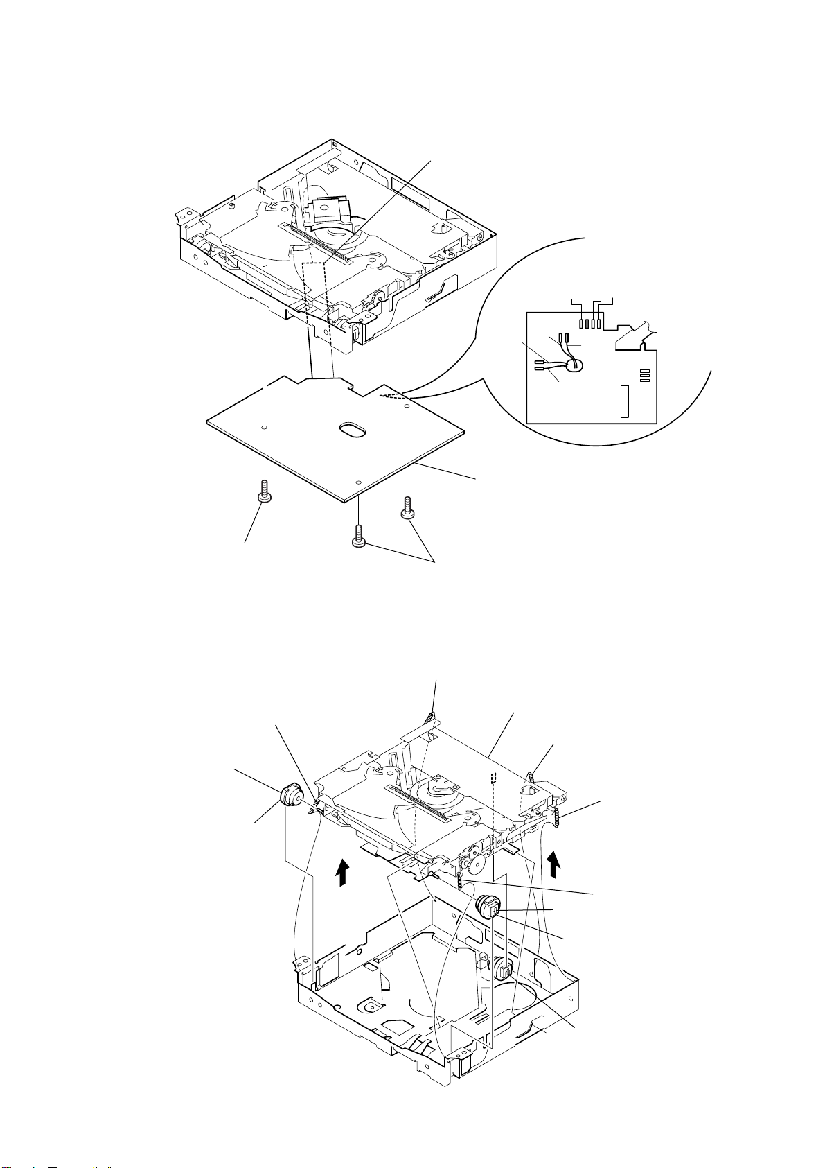
2-7. SERVO BOARD
5
PIC2 FLEXIBLE board
yellow
red
CDC-R30MP/X30MP
1
Removal the solders.
orange
blue
brawn
white
black
green
2
PTT 2x3
2-8. FLOATING BLOCK ASSY
1
8
claw
qs
oil damper
tension spring
0
4
SERVO board
3
screws (M1.7x4)
2
tension spring
ground point
qd
floating block aasy
3
tension spring
9
4
tension spring
7
claw
qa
5
tension spring
oil damper
6
claw
11
CDC-R30MP/X30MP
w
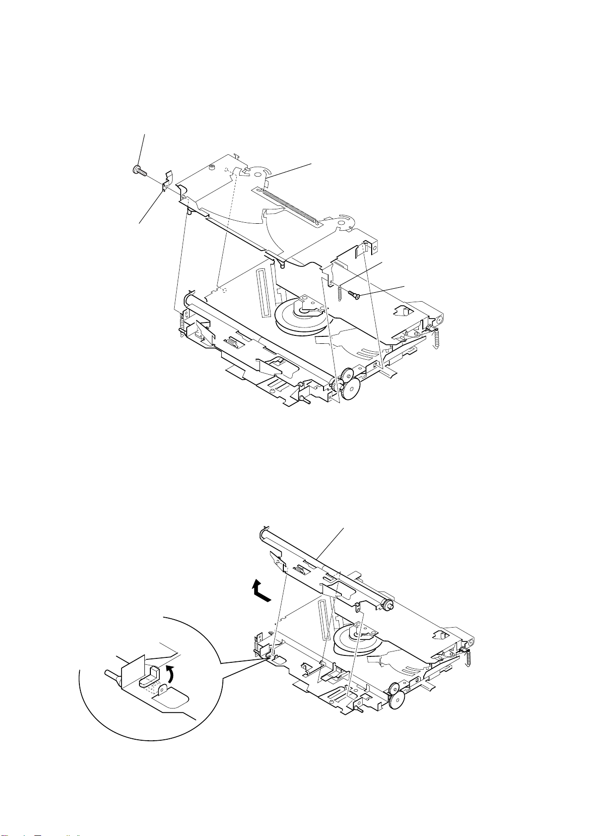
2-9. LEVER ASSY (CD UP HOLDER CNF)
1
P 1.4x2
2
leaf spring (roller)
5
lever assy (CD up holder CNF)
4
tension spring
3
special scre
2-10. LEVER (CD ROLLER) SUB ASSY
1
2
3
lever (CD roller) sub assy
12
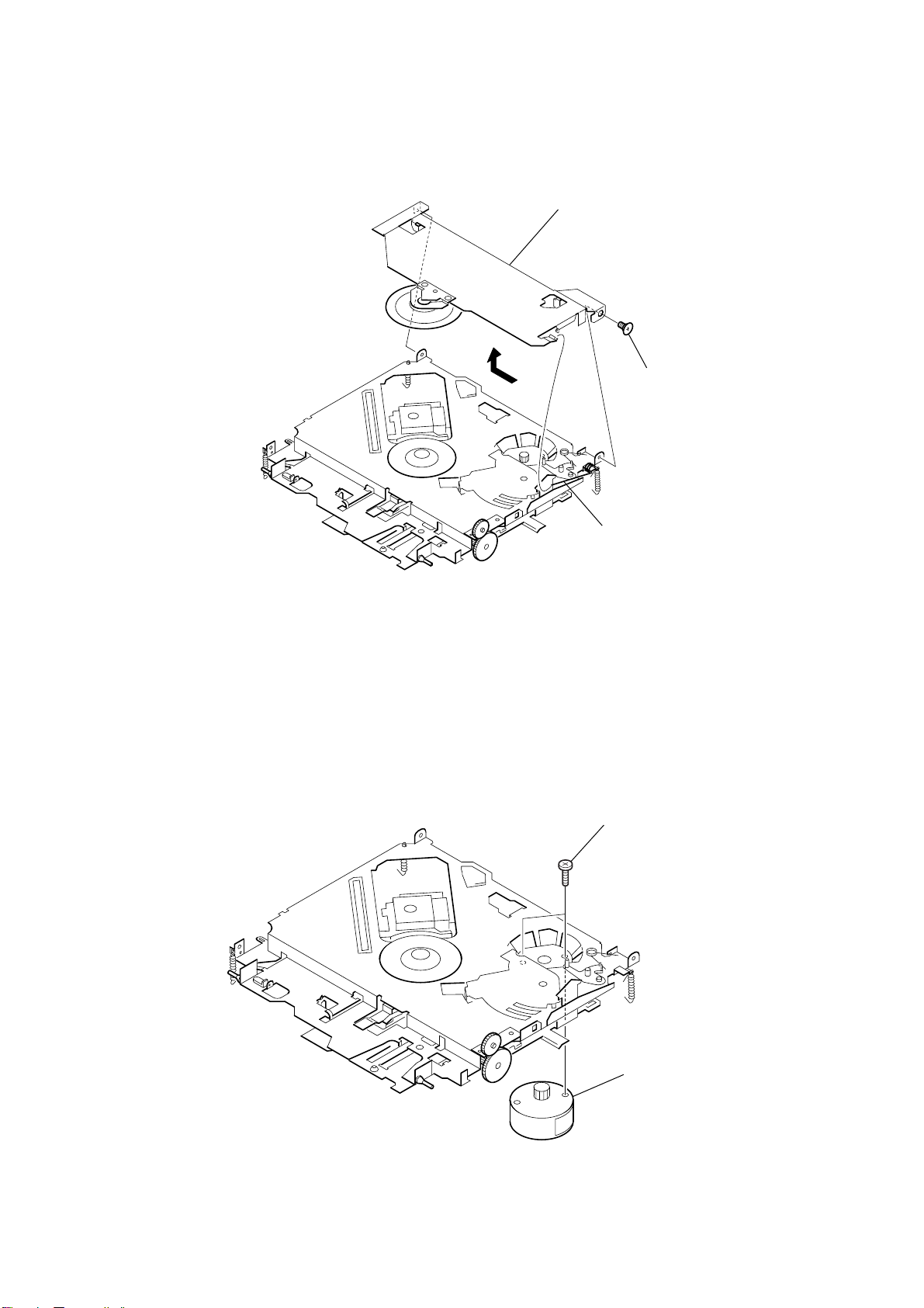
2-11. LEVER ASSY (CD HOLDER)
y
3
4
lever assy (CD holder)
2
special screw
CDC-R30MP/X30MP
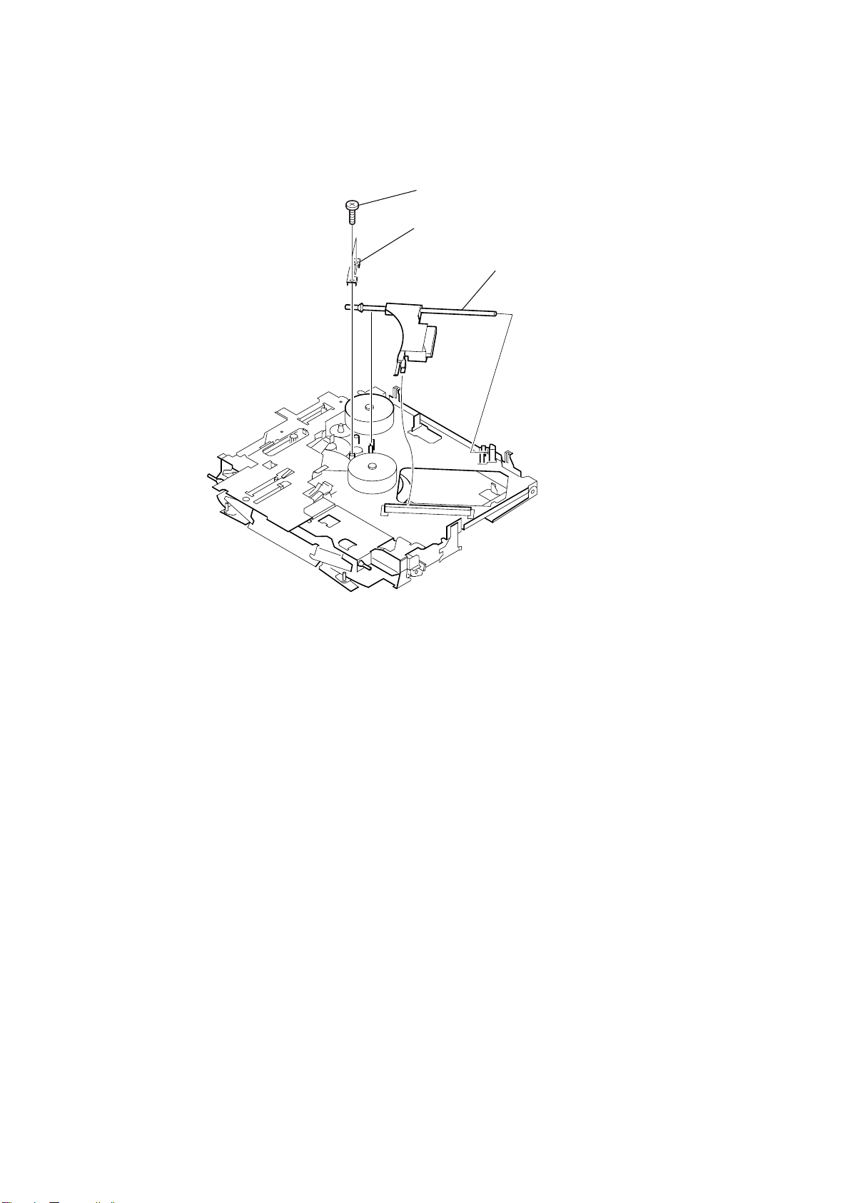
2-12. MOTOR (SLED) SUB ASSY
1
torsion spring
1
P 1.7x2
2
motor (sled) sub ass
13
CDC-R30MP/X30MP
y
2-13. PICK-UP SUB ASSY
1
B 1.4x5
2
leaf spring
3
pick-up sub ass
14
SECTION 3
ELECTRICAL ADJUSTMENT
RDS Adjustment (CDC-R30MP only)
Setting:98 MHz
31 dBµV (EMF)
1 kHz (Modulation Frequency)
45 kHz DEV
Check point: S.METER test point
Adjustment location: SFR101
Specification: 2.0±0.1 V
Procedure: Set to FM98.0 MHz and adjust SFR101 so that the test
point is 2.0±0.2 V.
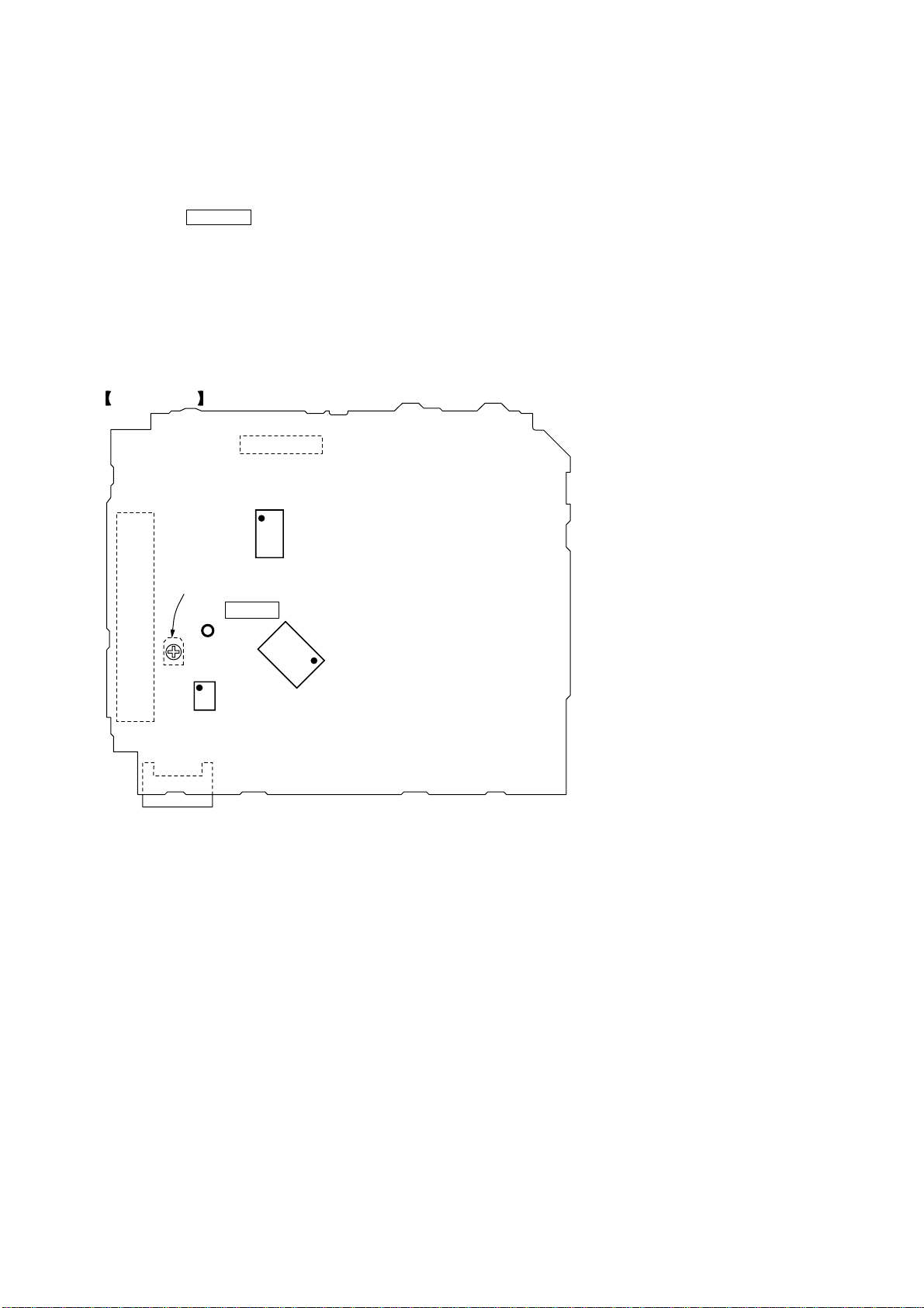
Adjustment Location:
MAIN BOARD (CONDUCTOR SIDE)
IC501
CDC-R30MP/X30MP
TU101
IC401
SFR101 RDS Adjustment
TP16 S.METER
IC901
IC151
CON702
15

CDC-R30MP/X30MP
SECTION 4
DIAGRAMS
4-1. IC PIN DESCRIPTIONS
• IC201 µPD63760GJ-8EN (RF AMP, DSP, DEC) (SERVO BOARD)
Pin No. Pin Name I/O Pin Description
1R GND — Ground pin for DRAM I/F
2 RST I Reset signal input from the mechanism control IC (IC301)
3 – 7 AB12 – AB8 I Address bus signal input from the mechanism control IC (IC301)
8 – 15 AD7 – AD0 I/O Address/data bus signal input from the mechanism control (IC301)
16 CS I Chip select signal input from the mechanism control IC (IC301)
17 ASTB I Address strob signal input from the mechanism control IC (IC301)
18 READ I Read control signal input from the mechanism control IC (IC301)
19 WRITE I Write control signal input from the mechanism control IC (IC301)
20 WAIT O Wait control signal output to the mechanism control IC (IC301)
21 INTQ O Interruption signal output to the mechanism control IC (IC301)
22 IFMODE I 16 bit/8 bit data bus change signal output
23 D VDD — Power supply pin for digital circuit (+3 V)
24 XTALEN1 I Oscillation permission pin (16.9344 MHz)
25 XTALEN2 I Oscillation permission pin (24.576 MHz)
26 DA VDD — Power supply pin for DAC (+3 V)
27 ROUT O R channel audio signal output
28 DA GND — Ground pin for DAC
29 R+ O R channel audio PDM signal output 1 Not used in this set. (Open)
30 R– O R channel audio PDM signal output 2 Not used in this set. (Open)
31 REGC — Capacitor connection pin for bandgap
32 L– O L channel audio PDM signal output 2 Not used in this set. (Open)
33 L+ O L channel audio PDM signal output 1 Not used in this set. (Open)
34 DA GND — Ground pin for DAC
35 LOUT O L channel audio signal output
36 DA VDD — Power supply pin for DAC (+3 V)
37 XVDD — Power supply pin for crystal oscillator (+3 V)
38 XTAL1 I I Crystal oscillator connection pin (16.9344 MHz)
39 XTAL1 O O Crystal oscillator connection pin (16.9344 MHz)
40, 41 XGND — Ground pin for crystal oscillator
42 XTAL2 O O Crystal oscillator connection pin (24.576 MHz) Not used in this set. (Open)
43 XTAL2 I I Crystal oscillator connection pin (24.576 MHz) Not used in this set. (Open)
44 XVDD — Power supply pin for crystal oscillator (+3 V)
45 D GND — Ground pin for digital circuit
46 DIN I Audio data signal input
47 DOUT O Audio data signal output Not used in this set. (Open)
48 SCKIN I Clock signal input for audio data
49 SCKO O Clock signal output for audio data Not used in this set. (Open)
50 LRCKIN I LRCK signal input for audio data
51 LRCK O LRCK signal output for audio data Not used in this set. (Open)
52 TESTX O Test output Not used. (Open)
53 RFOK O RFOK signal output to the mechanism control IC (IC301)
54 C16M O 16.9344 MHz output Not used in this set. (Open)
55 TESTEN — Connected to ground.
56 TEST4 — Connected to ground.
57 VDD — Power supply pin 1 for digital circuit (+3 V)
58 RFCK/HOLD O RFCK signal output/HOLD signal output Not used in this set. (Open)
59 WFCK/MIRR O WFCK signal output/MIRR signal output Not used in this set. (Open)
60 PLCK O PLCK signal output Not used in this set. (Open)
16
 Loading...