

Sony BVP-E30, BVP-E30P, BVP-E30WS, BVP-E30WSP Maintenance Manual

COLOR VIDEO CAMERA
BVP-E30
BVP-E30P
BVP-E30WS
BVP-E30WSP
MAINTENANCE MANUAL
Volume 1 1st Edition
Serial No. 100001 and Higher: BVP-E30
Serial No. 400001 and Higher: BVP-E30P
Serial No. 100001 and Higher: BVP-E30WS
Serial No. 400001 and Higher: BVP-E30WSP

! WARNING
This manual is intended for qualified service personnel only.
To reduce the risk of electric shock, fire or injury, do not perform any servicing other than that
contained in the operating instructions unless you are qualified to do so. Refer all servicing to
qualified service personnel.
! WARNUNG
Die Anleitung ist nur für qualifiziertes Fachpersonal bestimmt.
Alle War tungsarbeiten dürfen nur von qualifiziertem Fachpersonal ausgeführt werden. Um die
Gefahr eines elektrischen Schlages, Feuergefahr und Verletzungen zu vermeiden, sind bei
Wartungsarbeiten strikt die Angaben in der Anleitung zu befolgen. Andere als die angegeben
Wartungsarbeiten dürfen nur von Personen ausgeführt werden, die eine spezielle Befähigung
dazu besitzen.
! AVERTISSEMENT
Ce manual est destiné uniquement aux personnes compétentes en charge de l’entretien. Afin
de réduire les risques de décharge électrique, d’incendie ou de blessure n’effectuer que les
réparations indiquées dans le mode d’emploi à moins d’être qualifié pour en effectuer d’autres.
Pour toute réparation faire appel à une personne compétente uniquement.
For the customers in the Netherlands
Voor de klanten in Nederland
Dit apparaat bevat een MnO
back-up.
Raadpleeg uw leverancier over de verwijdering van de
batterij op het moment dat u het apparaat bij einde
levensduur afdankt.
Gooi de batterij niet weg. maar lever hem in als KCA.
Bij dit produkt zijn batterijen geleverd.
Wanneer deze leeg zijn, moet u ze niet
weggooien maar inleveren als KCA.
2-Li batterij voor memory
Für Kunden in Deutschland
Entsorgungshinweis: Bitte werfen Sie nur entladene
Batterien in die Sammelboxen beim Handel oder den
Kommunen. Entladen sind Batterien in der Regel dann,
wenn das Gerät abschaltet und signalisiert “Batterie
leer” oder nach längerer Gebrauchsdauer der Batterien
“nicht mehr einwandfrei funktioniert”. Um
sicherzugehen, kleben Sie die Batteriepole z.B. mit
einem Klebestreifen ab oder geben Sie die Batterien
einzeln in einen Plastikbeutel.
BVP-E30/E30P M-V1
CAUTION
ADVARSEL!
Lithiumbatteri-Eksplosionsfare ved fejlagtig
håndtering.
Udskiftning må kun ske med batteri
af samme fabrikat og type.
Levér det brugte batteri tilbage til leverandøren.
Danger of explosion if battery is incorrectly replaced.
Replace only with the same or equivalent type
recommended by the manufacturer.
Dispose of used batteries according to the
manufacturer’s instructions.
Vorsicht!
Explosionsgefahr bei unsachgemäßem Austausch
der Batterie.
Ersatz nur durch denselben oder einen vom
Hersteller empfohlenen ähnlichen Typ. Entsorgung
gebrauchter Batterien nach Angaben des
Herstellers.
ATTENTION
Il y a danger d’explosion s’il y a remplacement
incorrect de la batterie.
Remplacer uniquement avec une batterie du même
type ou d’un type équivalent recommandé par le
constructeur.
Mettre au rebut les batteries usagées conformément
aux instructions du fabricant.
ADVARSEL
Lithiumbatteri - Eksplosjonsfare.
Ved utskifting benyttes kun batteri som
anbefalt av apparatfabrikanten.
Brukt batteri returneres
apparatleverandøren.
VARNING
Explosionsfara vid felaktigt batteribyte.
Använd samma batterityp eller en likvärdig typ
som rekommenderas av apparattillver karen.
Kassera använt batteri enligt gällande
föreskrifter.
VAROITUS
Paristo voi räjähtää jos se on virheellisesti
asennettu.
Vaihda paristo ainoastaan laitevalmistajan
suosittelemaan tyyppiin.
Hävitä käytetty paristo valmistajan ohjeiden
mukaisesti.
BVP-E30/E30P M-V1
1 (P)
For the customers in Japan
For the customers in the U.S.A. and Canada
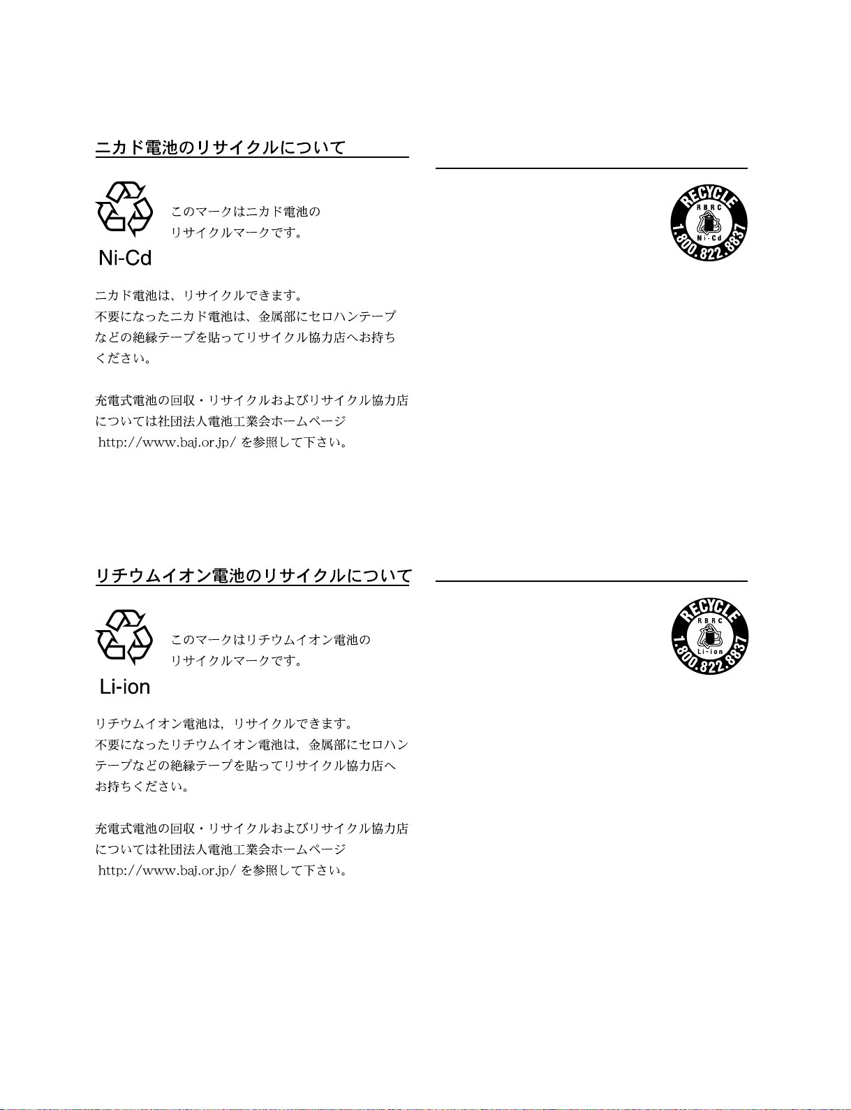
RECYCLING NICKEL-CADMIUM
BATTERIES
Nickel Cadmium batteries are
recyclable. You can help preserve our
environment by returning your unwanted
batteries to your nearest point for
collection, recycling or proper disposal.
Note: In some areas the disposal of
nickel cadmium batteries in household or business trash
may be prohibited.
RBRC (Rechargeable Battery Recycling Corporation)
advises you about spent battery collection by the
following phone number.
Call toll free number: 1-800-822-8837
(United States and Canada only)
Caution: Do not handle damaged or leaking nickelcadmium batteries.
For the customers in Japan
For the customers in the U.S.A. and Canada
RECYCLING LITHIUM-ION BATTERIES
Lithium-Ion batteries are recyclable.
You can help preserve our environment
by returning your used rechargeable
batteries to the collection and recycling
location nearest you.
For more information regarding recycling of rechargeable batteries, call toll free
1-800-822-8837, or visit http://www.rbrc.org/
Caution: Do not handle damaged or leaking Lithium-Ion
batteries.
2 (P)
BVP-E30/E30P M-V1

Table of Contents
Manual Structure
Purpose of this manual ........................................................................................ 5 (E)
Related manuals................................................................................................... 5 (E)
Contents ............................................................................................................... 6 (E)
1. Service Overview
1-1. Note on Service.....................................................................................1-1 (E)
1-1-1. Confirming the ROM Version .............................................1-1 (E)
1-1-2. Compatibility of File Data ...................................................1-1 (E)
1-1-3. Error Messages Displayed when Memory Stick is Used .....1-1 (E)
1-1-4. Note on PA-272/273/274 Boards .........................................1-1 (E)
1-1-5. Description on Backup Battery ............................................1-2 (E)
1-1-6. Description on CCD Block Number ....................................1-2 (E)
1-1-7. Notes on Spare Parts ............................................................1-2 (E)
1-1-8. Unleaded Solder...................................................................1-2 (E)
1-2. Connector Input/Output Signals............................................................1-3 (E)
1-3. Connection Connector...........................................................................1-7 (E)
1-4. Function of Internal Switches ...............................................................1-7 (E)
1-5. Remove and Installation of Exterior Parts ............................................1-9 (E)
1-6. Location of Printed Wiring Boards.......................................................1-9 (E)
1-7. Circuit Description..............................................................................1-10 (E)
1-7-1. CCD Block (PA-272/273/274 Boards, TG-229 Board,
and NR-72 Board) ..............................................................1-10 (E)
1-7-2. Video Signal System (VA-226 Board, DPR-261 Board,
and IF-969 Board) ..............................................................1-11 (E)
1-7-3. System Control (AT-148 Board)........................................1-12 (E)
1-7-4. Power Supply Block (DC-DC Converter)
(RE-201 Board) ..................................................................1-13 (E)
1-8. Diagnosis.............................................................................................1-14 (E)
1-9. Contents of the EEPROM and FRAM Data .......................................1-15 (E)
1-10. Adjustment and Setting Items After Replacement of Board...............1-16 (E)
1-10-1. CCD Unit ...........................................................................1-16 (E)
1-10-2. TG-229 Board ....................................................................1-16 (E)
1-10-3. NR-72 Board ......................................................................1-16 (E)
1-10-4. VA-226 Board ....................................................................1-16 (E)
1-10-5. DPR-261 Board ..................................................................1-16 (E)
1-10-6. AT-148 Board ....................................................................1-16 (E)
1-11. Upgrading the Software ......................................................................1-17 (E)
1-11-1. Upgrading MAIN Program ................................................1-17 (E)
1-11-2. Upgrading BOOT Program ................................................1-17 (E)
1-12. Setting Scene File Number..................................................................1-18 (E)
1-13. Removing and Reinstalling the Flexible Card Wires..........................1-19 (E)
BVP-E30/E30P M-V1
1 (E)

1-14. How to Extend the Circuit Board........................................................ 1-20 (E)
1-14-1. Extending the DPR-261 Board...........................................1-20 (E)
1-14-2. Extending the DC-DC Converter .......................................1-20 (E)
1-14-3. Extending the CCD Block..................................................1-21 (E)
1-15. Inspection and Maintenance................................................................1-22 (E)
1-15-1. Recommended Replacement Parts .....................................1-22 (E)
1-15-2. Cares after Using under Special Environment ...................1-24 (E)
1-15-3. Fixtures...............................................................................1-25 (E)
2. Replacement of Main Parts
2-1. Replacing the CCD Block and Component Parts .................................2-1 (E)
2-1-1. Replacing the CCD Unit ......................................................2-1 (E)
2-1-2. Positioning Adjustment for Filter Knob...............................2-3 (E)
2-1-3. Replacing the Boards Inside the CCD Unit .........................2-4 (E)
2-1-4. Adjusting Filter Position After Replacing the
DR-536 Board ......................................................................2-6 (E)
2-2. Replacing the VF Connector.................................................................2-7 (E)
2-3. Replacing the Illuminated ASSIGNABLE Switch ...............................2-7 (E)
2-4. Replacing the RET/INCOM Switch......................................................2-9 (E)
2-5. Removing the V Shoe Bracket..............................................................2-9 (E)
2-6. Replacing the MENU SELECT Knob/MENU Switch/
DISPLAY Switch................................................................................ 2-10 (E)
2-7. Replacing the LENS Connector..........................................................2-11 (E)
2-8. Replacing the TEST OUT Connector .................................................2-11 (E)
2-9. Replacing the Side Switch Panel Block..............................................2-12 (E)
2-10. Replacing the Front Switch Panel Block ............................................2-12 (E)
2-11. Replacing the MIC Connector ............................................................2-13 (E)
2-12. Replacing the DC-DC Converter ........................................................ 2-13 (E)
2-13. Replacing the MB-953 Board .............................................................2-14 (E)
2-14. Replacing the CN-2204 Board ............................................................2-15 (E)
2-15. Replacing the Memory Stick Case (CN-2206 Board).........................2-16 (E)
2 (E)
3. Setup Menu
3-1. Setup Menu ...........................................................................................3-1 (E)
3-2. TOP Menu.............................................................................................3-3 (E)
3-3. OPERATION Menu..............................................................................3-4 (E)
3-4. PAINT Menu.......................................................................................3-13 (E)
3-5. MAINTENANCE Menu .....................................................................3-26 (E)
3-6. FILE Menu..........................................................................................3-35 (E)
3-7. DIAGNOSIS Menu.............................................................................3-40 (E)
3-8. SERVICE Menu..................................................................................3-40 (E)
BVP-E30/E30P M-V1

4. File System
4-1. File Structure.........................................................................................4-1 (E)
4-2. Operator File .........................................................................................4-2 (E)
4-3. Preset Operator File...............................................................................4-3 (E)
4-4. Scene File..............................................................................................4-4 (E)
4-5. Reference File .......................................................................................4-6 (E)
4-6. Lens File................................................................................................4-8 (E)
4-7. OHB File .............................................................................................4-10 (E)
4-8. File Items.............................................................................................4-12 (E)
5. Electrical Alignment
5-1. Preparation ............................................................................................5-1 (E)
5-1-1. Equipment Required............................................................. 5-1 (E)
5-1-2. Notes on Adjustment............................................................5-2 (E)
5-1-3. Connection ...........................................................................5-2 (E)
5-1-4. Initial Settings ......................................................................5-3 (E)
5-1-5. Presetting Compensation Data .............................................5-4 (E)
5-1-6. SERVICE Menu...................................................................5-4 (E)
5-1-7. Maintaining the Grayscale Chart .........................................5-5 (E)
5-2. VA-226 Board Adjustment ...................................................................5-7 (E)
5-2-1. Black Balance Adjustment...................................................5-7 (E)
5-2-2. Flare Offset Adjustment.......................................................5-7 (E)
5-2-3. Offset Adjustment ................................................................5-8 (E)
5-3. PA-272/273/274 Boards Adjustment ....................................................5-9 (E)
5-3-1. PA Gain Adjustment ............................................................5-9 (E)
5-4. DPR-261 Board Adjustment ...............................................................5-10 (E)
5-4-1. Video Level Adjustment (1)...............................................5-10 (E)
5-4-2. Video Level Adjustment (2)...............................................5-11 (E)
5-4-3. TEST OUT Level Adjustment ...........................................5-12 (E)
5-4-4. SC Frequency Adjustment .................................................5-13 (E)
5-5. RPN Pixel Concealment......................................................................5-14 (E)
5-6. RPN Compensation Adjustment .........................................................5-15 (E)
5-7. White Vertical Line Compensation.....................................................5-16 (E)
5-8. V-SUB Voltage Adjustment ...............................................................5-17 (E)
5-9. V-REG Voltage Adjustment ...............................................................5-18 (E)
BVP-E30/E30P M-V1
3 (E)


Purpose of this manual
Related manuals
Manual Structure
This manual is the maintenance manual volume 1 of Color Video Camera BVP-E30/
E30P/E30WS/E30WSP.
This manual is intended for use by trained system and service engineers, and is
provided information that is premised parts levels service for this unit.
Besides this maintenance manual volume 1, the following manuals are available.
..
. Operation Manual (Supplied with this unit)
..
This manual is necessary for the use and the operation of this unit.
Part No.: 3-854-245-XX
..
. CD-ROM Manual (Supplied with this unit)
..
This manual contains the operation manual of BVP-E30/E30WS, the operation
manual of each peripheral equipment included in BVP-E30 series, and the maintenance manual of partial equipment (camera adaptor and the like).
Part No.: 3-854-379-XX
..
. Maintenance Manual Volume 2 (Available on request)
..
This manual is provided information that is premised the parts level service
(exploded views, block diagrams, board layouts, schematic diagrams, detailed
parts lists and the like.) for this unit.
If this manual is required, please contact to your local Sony Sales Office/Service
Center.
Part No.: 9-968-050-XX
..
. “Semiconductor Pin Assignments” CD-ROM (Available on request)
..
This “Semiconductor Pin Assignments” CD-ROM allows you to search for
semiconductors used in Communication B&P Company equipment.
Semiconductors that cannot be searched for on this CD-ROM are listed in the
maintenance manual for the corresponding unit. The maintenance manual contains
a complete list of all semiconductors and their ID Nos., and thus should be used
together with the CD-ROM.
Part number: 9-968-546-XX
BVP-E30/E30P M-V1
5 (E)

Contents
The following is a summary of the sections of this manual.
Section 1 Service Overview
Describes the location of major parts, on-board, switches, tools, fixtures, adjustments/setup after board replace, etc.
Section 2 Parts Replacement
Describes the replacement procedure of circuit board, CCD unit, connectors,
switches and others.
Section 3 Setup Menu
Describes the setup menu, etc.
Section 4 File System
Describes the file structure, etc.
Section 5 Electrical Alignment
Describes electrical adjustment necessary for maintenance of the unit or replacement
of parts.
6 (E)
BVP-E30/E30P M-V1

Section 1
Service Overview
1-1. Note on Service
1-1-1. Confirming the ROM Version
When connecting any of the peripheral equipment in the
following list to this unit, be sure to check that the version
of ROM of each peripheral device to be connected.
If ROM version is lower than the specified below, be sure
to perform ROM replacement.
Model Ref No. ROM version
MSU-700A IC5, IC6/CPU-293 board Ver. 1.20 and
higher
MSU-750 IC5, IC6/CPU-286 board Ver. 1.20 and
higher
CCU-700A IC1004/AT-88 board Ver. 2.90 and
higher
CCU-550A IC133/AT-111 board Ver. 3.00 and
higher
CNU-700 IC4, IC5/AT-89 or Ver. 3.30 and
AT-89A board higher
CNU-500 IC4, IC5/AT-100 board Ver. 2.90 and
higher
RCP-720 Series IC10/MPU-79 board Ver. 2.80 and
RCP-730 Series higher
RCP-740 Series
RM-B750 Series Ver. 1.01 and
higher
RCP-750 Series Ver. 1.01 and
higher
RM-B150 IC4/CPU-266 board Ver. 1.20 and
higher
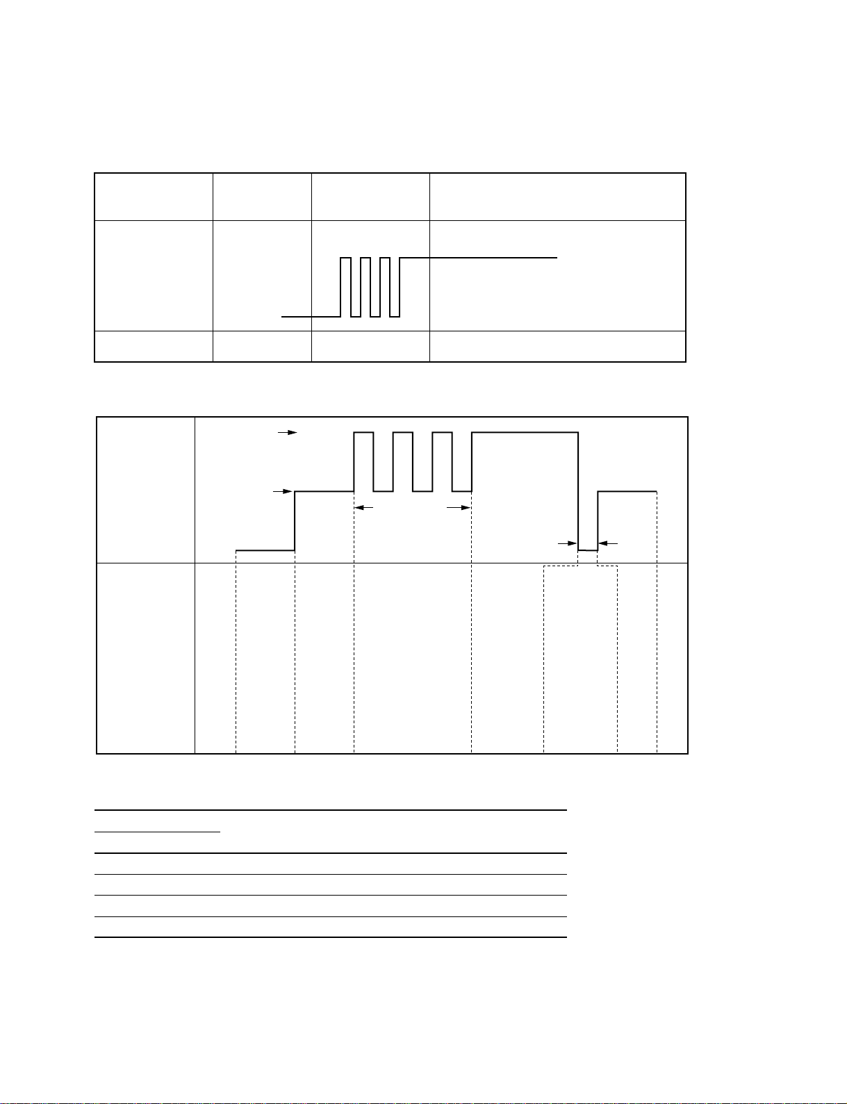
1-1-3. Error Messages Displayed when
Memory Stick is Used
Describes the error messages displayed when the data is
stored or read using a memory stick in the table below.
Error message Description
NO MEMORY STICK No memory stick is inserted.
FORMAT ERROR The memory stick is not formatted.
OTHER MODEL’S FILE The memory stick contains data
cannot be read by this unit.
FILE NOT FOUND No data is stored in the memory
stick.
FILE ERROR Circuit or memory stick fault and/or
the data in the memory stick fault.
1-1-4. Note on PA-272/273/274 Boards
The PA-272/273/274 boards cannot be replaced as the
mounted board level. If the component part mounted on
the board cannot be replaced, replace with the whole CCD
unit.
1-1-2. Compatibility of File Data
The file data does not have compatibility with other
cameras.
When using the file data stored in the memory stick or the
IC memory card (for MSU), make sure that the file data for
BVP-E10 series or BVP-E30 series are stored.
(For details on the file system, refer to Section 4.)
BVP-E30/E30P M-V1
1-1 (E)

1-1-5. Description on Backup Battery
1-1-7. Notes on Spare Parts
w
The lithium battery is critical part to safe operation.
Replace the component with Sony part whose part number
appears in the manual published by Sony.
If the component is replaced by any part other than the
specified ones, this may cause a fire or electric shock.
c
When replacing the lithium battery, ensure that the battery
is installed with + and _ poles connected to the correct
terminals. An inconnect connection may cause an explosion or leakage of fluid result in physical damage in the
surrounding materials.
A lithium battery on the AT-148 board is used to back up
the date data to be stored in the memory stick. Reset the
date data using the DATE/TIME page (Refer to Section
3-5) in the MAINTENANCE menu after replacing the
dead battery.
Replacement part : BT1 (AT-148 board)
Description : CR-2032
(Lithium battery)
Parts number : ! 1-528-174-31
Recommended replacement period : Every 7 years
m
. When replacing the AT-148 board, it is recommended to
replacing the battery at the same time.
. Resetting the date data is required even when the battery
is disconnected from the battery holder.
1. Safety Related Components Warning
w
Components marked ! are critical to safe operation.
Therefore, specified parts should be used in the case of
replacement.
2. Standardization of Parts
Some repair parts supplied by Sony differ from those
used for the unit. These are because of parts commonality and improvement.
Parts list has the present standardized repair parts.
3. Stock of Parts
Parts marked with “o” at SP (Supply Code) column of
the spare parts list may not be stocked.
Therefore, the delivery date will be delayed.
4. Harness
The harness with which the part number is not described is not registered as the service parts. Replace
with the component part described in the lists.
1-1-8. Unleaded Solder
Boards requiring use of unleaded solder are printed with a
lead free mark (LF) indicating the solder contains no lead.
(Caution: Some printed circuit boards may not come
printed with the lead free mark due to their particular size.)
: LEAD FREE MARK
1-1-6. Description on CCD Block Number
Every CCD unit has its own ID number called CCD block
number. It shows the CCD block type and serial number of
the CCD block.
The CCD block number label is put in the CCD unit.
As for the replacement procedures of CCD block, refer to
Section 2-1-1. “Replacing the CCD Block”.
AKA xxxxx
Serial number for CCD block
CCD block type
1-2 (E)
m
. Be sure to use the unleaded solder for the printed circuit
board printed with the lead free mark.
. The unleaded solder melts at a temperature about 40 dC
higher than the ordinary solder, therefore, it is recommended to use the soldering iron having a temperature
regulator.
. The ordinary soldering iron can be used but the iron tip
has to be applied to the solder joint for a slightly longer
time. The printed pattern (copper foil) may peel away if
the heated tip is applied for too long, so be careful.
BVP-E30/E30P M-V1
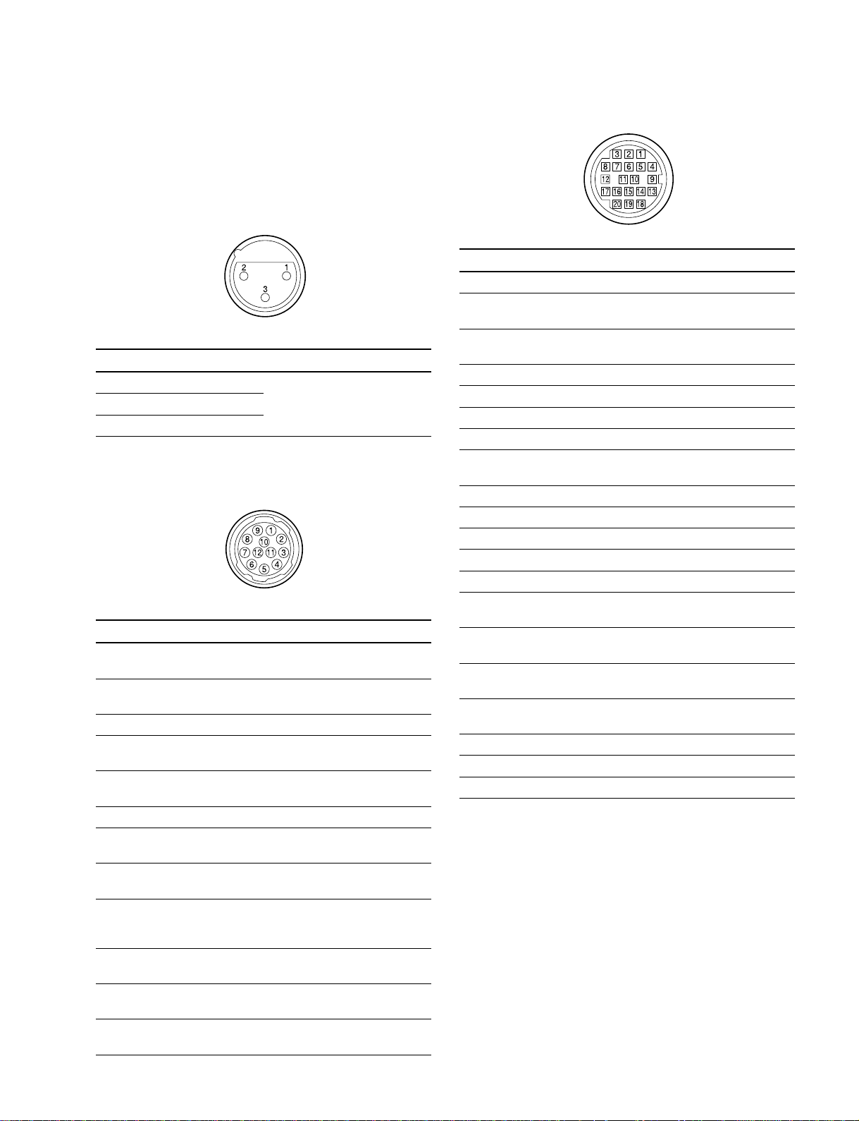
1-2. Connector Input/Output Signals
TEST OUT
BNC 75 Z 1.0 V p-p
VF (20P FEMALE)
MIC IN (3P FEMALE)
(EXTERNAL VIEW)
No. SIGNAL SPECIFICATIONS
1 MIC IN (G) _60 dBu High impedance
2 MIC IN (X)
3 MIC IN (Y)
balanced
(0 dBu = 0.775 Vrms)
LENS (12P FEMALE)
(EXTERNAL VIEW)
No. SIGNAL SPECIFICATIONS
1 RET VIDEO ENABLE IN ENABLE: 0 V
2 RET 2 ENABLE IN ENABLE: 0 V
3 GND GND for UNREG
4 AUTO +5 V OUT AUTO: +5 V
5 IRIS CONT OUT +3.4 V (F16) to
6 UNREG OUT +10.5 V to +17 V
7 IRIS POSITION IN +3.4 V (F16) to
8 AUTO/MANU OUT AUTO IRIS: 0 V
9 EXTENDER ON/OFF IN EX 2 ON: 0 V
10 ZOOM POSITION IN WIDE: +2 V
11 SER DATA OUT H: +5V
12 SER DATA IN H: +5V
BVP-E30/E30P M-V1
DISABLE: +5 V or OPEN
DISABLE: +5 V or OPEN
MANU: 0 V or OPEN
+6.2 V (F2.8)
+6.2 V (F2.8)
MANUAL IRIS: +5 V
EX 0.8 ON: +1.8 V
OFF: +4.8 V
TELE: +7 V
L: 0V
L: 0V
(EXTERNAL VIEW)
No. SIGNAL SPECIFICATIONS
1 NC No connection
2 ABNORMAL IND OUT L: Indicator lights
3 16:9 MODE OUT H: NORMAL (4:3)
4 NC No connection
5 COMP/VBS SW IN/OUT *
6 CCIR/EIA OUT H: CCIR, L: EIA
7 NC No connection
8 G TALLY OUT H: Indicator lights
9 NC No connection
10 Y (X) OUT 1 V p-p, VF: Zi = 1 kZ
11 ZEBRA ON IN H: OFF, L: ON
12 VF VIDEO OUT (X) 1.0 V p-p, VF: Zi = 1 kZ
13 NC No connection
14 B-Y (X) OUT 700 mV p-p, VF: Zi = 1 kZ,
15 R-Y (X) OUT 700 mV p-p, VF: Zi = 1 kZ,
16 BATT IND OUT H: Indicator lights
17 TALLY IND OUT H: Indicator lights
18 +9.3 V (VF) OUT REG +9.3 V
19 GND GND
20 UNREG OUT +10.5 V to +17 V
OPEN: Indicator goes out
L: WIDE (16:9)
Note1
L: Indicator goes out
75 % color-bars
75 % color-bars
L: Indicator goes out
L: Indicator goes out
Note1: Specification of COMP/VBS SW Signal
When powering on, the microcomputer of the camera identifies a
viewfinder in use by detecting the voltage at pin 5.
H: Color VF, L: B/W VF
. In use of B/W VF
Voltage control of pin 5 is disabled during operation.
Switching between the return video signal and monochrome signal for the viewfinder is done by the camera
and selected signal is output at pin 12 to the viewfinder.
. In use of Color VF
By controlling the voltage at pin 5 during operation,
switching between the decoded return video signal and
the camera component signal is done in the viewfinder.
H: Camera, L: Return video
1-3 (E)
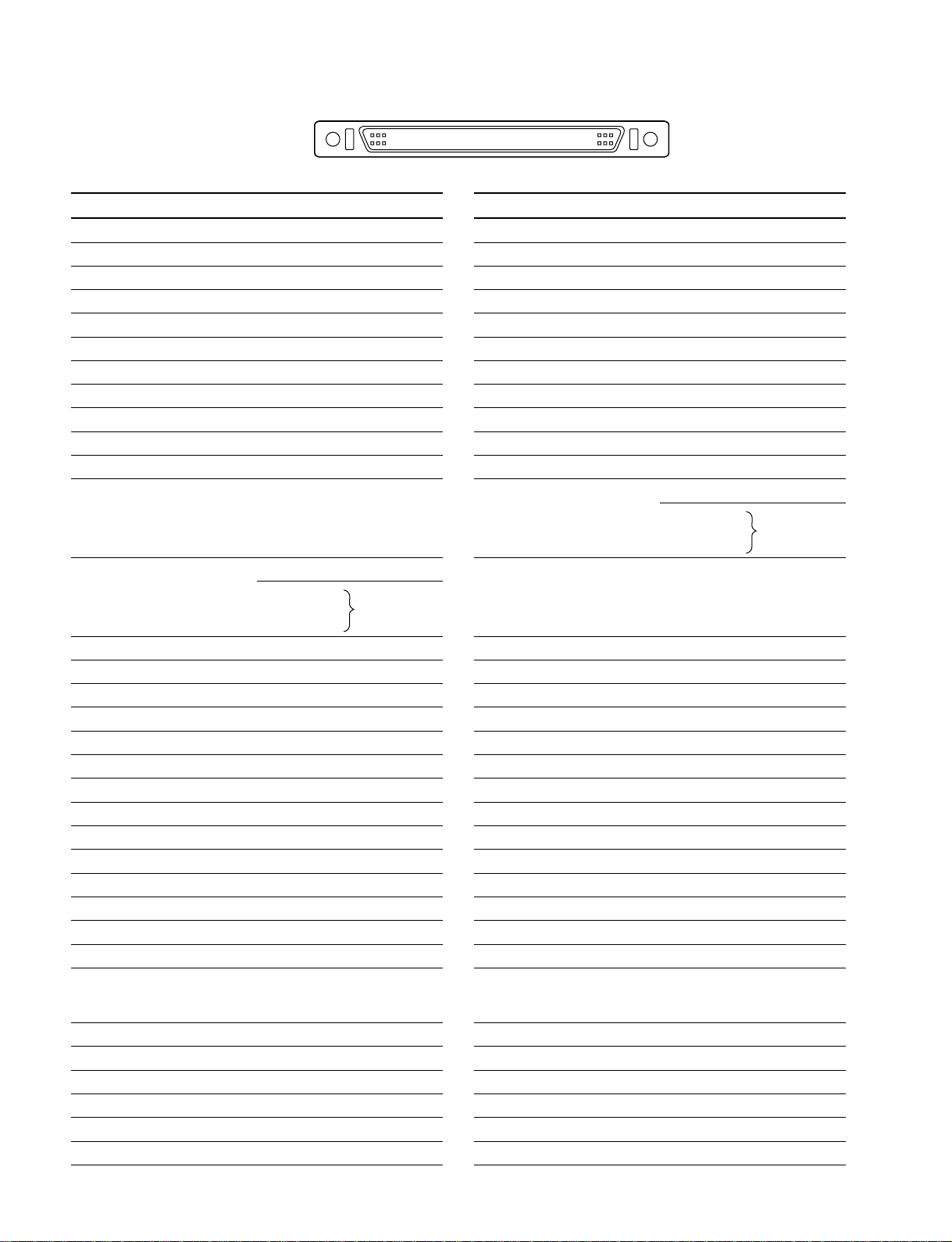
ANALOG CA (68P FEMALE)
34
68
*: In connection with CCU, **: In connection with VTR
No. SIGNAL SPECIFICATIONS
1 UNREG GND GND for UNREG
2 UNREG GND GND for UNREG
3 VF UNREG GND GND for VF UNREG
4 LENS UNREG GND GND for LENS UNREG
5 UNREG IN 10.5 V to 17 V
6 UNREG IN 10.5 V to 17 V
7 VF UNREG IN 10.5 V to 17 V
8 LENS UNREG IN 10.5 V to 17 V
9 NC No connection
10 NC No connection
11 VBS OUT (G) GND for VBS VIDEO
12 Y OUT (X) VS 1.0 V p-p, Zo = 75 Z
13 B-Y OUT (X) 700 mV p-p, with sample 350 mV*
756 mV p-p (J)
700 mV p-p (UC) **
525 mV p-p (CE)
14 NC No connection
15 NC No connection
16 VBS GENLOCK IN (X) 1.0 V p-p ±6 dB
17 RET VIDEO IN (G) GND for RET VIDEO
18
MONITOR VIDEO OUT (X)
19 BATTERY ALARM IN Zi = 300 Z *
20 NC No connection
21
AUDIO CH1 CONT OUT
22 MIC 1 OUT (Y) Zo < 600 Z, _60 dBu balanced
23 NC No connection
24 SKIN TONE GATE OUT 1.0 V p-p
25 TAPE REM IN *
26 VTR SYNC OUT +
27 RET EN OUT
28 PB REF IN PB; +4.5 V,
29 H CONT IN 0 V to 5 V, Analog
30 ANALOG GND
31 DIGITAL HD OUT 3.3 V p-p for Digital
32 COM CONT IN 5 V p-p
33 IIC CLOCK OUT (CA) 5 V p-p
34 NC No connection
VS 1.0 V p-p, Zo = 75 Z
Note 2
0 V (0 dB) to 7 V (_50 dB or less)
Note 4
5.0 V p-p Negative pulse, Zo < 100 Z
ENABLE; 0 V, DISABLE; +5 V or OPEN
CAM; 0 V or OPEN
1-4 (E)
1
(EXTERNAL VIEW)
35
No. SIGNAL SPECIFICATIONS
35 UNREG GND GND for UNREG
36 UNREG GND GND for UNREG
37 VF UNREG GND GND for VF UNREG
38 LENS UNREG GND GND for LENS UNREG
39 UNREG IN 10.5 V to 17 V
40 UNREG IN 10.5 V to 17 V
41 VF UNREG IN 10.5 V to 17 V
42 LENS UNREG IN 10.5 V to 17 V
43 NC No connection
44 NC No connection
45 VBS OUT (X) 1.0 V p-p ±10 %, Zo = 75 Z
46 R-Y OUT (X) 700 mV p-p, with sync 350 mV*
756 mV p-p (J)
700 mV p-p (UC) **
525 mV p-p (CE)
47 Y/R-Y/B-Y GND GND for Y/R-Y/B-Y
48 NC No connection
49 NC No connection
50 VBS GENLOCK IN (G) GND for GENLOCK/H CONT IN
51 RET VIDEO IN (X) 1.0 V p-p, Zi = 1 kZ
52
MONITOR VIDEO OUT (G)
53 VTR START/STOP OUT Zo < 10 kZ
54 NC No connection
55 MIC 1 OUT (G) GND for CAM MIC
56 MIC 1 OUT (X) Zo < 600 Z, _60 dBu balanced
57 NC No connection
58 NC No connection
59 AUDIO LEVEL IN Zi > 1 kZ (_15 dBu at 0 VU)
60 NC No connection
61 NC No connection
62 REC TALLY IN ON; +5 V,
63 VTR SAVE OUT
64 GND
65 NC No connection
66 COM DATA OUT 5 V p-p
67 IIC DATA IN/OUT (CA) 5 V p-p, 4700 Z, Pull up
68 NC No connection
GND for MONITOR VIDEO
OFF; +2.5 V or 0 V,
Zi > 20 kZ *
SAVE; +4.5 V, STANDBY; 0 V, Zo < 10 kZ
Note 3
(0 dBu = 0.775 Vrms)
BVP-E30/E30P M-V1
Note 2 : Specifications of BATT ALARM Signal
VTR has a battery voltage detection and waring signal generation circuits and it sends the signal shown
below to the camera.
Battery Terminal
Voltage
(VTR internal battery)
Input Signal at
Pin 19
LED on Viewfinder
12.0—11.1 V dc 11.1—10.8 V dc
1.0 ±0.2 Hz
duty 50 ±10 %
0 V
Stays out Blinks at 1 Hz Lights up
Note 3 : Specifications of REC TALLY Signal
+1
5.0
Input Signal at
Pin 62
VTR Action
_0.5 V dc
2.5 ±0.5 V dc
0 ±0.3 V dc
Power
OFF
Power ONWhen VTR changes
10.8 V dc—
REC TALLY
signal
1.0 ±0.2 Hz
duty 50 ±10 %
from POWER SAVE
to REC START mode,
or when the servo is
lost
REC RESET signal
10—100 msec
When VTR
changes from
STANDBY to
REC START
mode, or in
REC mode
At the end of
tape or When
VTR is put
into STOP
mode by itself
(REC RESET
signal does
not appear
when VTR is
put into STOP
mode by
operating the
camera)
2—3 V dc
across 300 Z
STOP
mode
Note 4 : Specifications of TAPE REM Signal
Tape Remaining (VTR) Input Signal at Pin 25 Remark
TAPE1 TAPE2
+5 V +5 V +3.4 V
+5 V 0 V +3.1 V G TALLY lamp lights at +3.1 V
0 V +5 V +2.2 V
0 V 0 V 0 V
BVP-E30/E30P M-V1
1-5 (E)
DIGITAL CA (68P FEMALE)
34
68
No. SIGNAL SPECIFICATIONS
1 G (L) OUT
2 G (2) OUT
3 G (4) OUT 2.5 V p-p
4 G (6) OUT
5 G (8) OUT
6 R (L) OUT
7 R (2) OUT
8 R (4) OUT 2.5 V p-p
9 R (6) OUT
10 R (8) OUT
11 B (L) OUT
12 B (2) OUT
13 B (4) OUT 2.5 V p-p
14 B (6) OUT
15 B (8) OUT
16 DIGITAL GND GND for DIGITAL
17
DIGITAL BLANKING OUT
3.3 V p-p
18 DIGITAL SYNC OUT 3.3 V p-p
19 NC No connection
20 NC No connection
21 NC No connection
22 NC No connection
23 NC No connection
24 NC No connection
25 NC No connection
26 NC No connection
27 NC No connection
28 NC No connection
29 NC No connection
30 NC No connection
31 NC No connection
32 NC No connection
33 (Reserve)
34 18 MHz OUT (G) GND for 18 MHz
1
35
(EXTERNAL VIEW)
No. SIGNAL SPECIFICATIONS
35 G (1) OUT
36 G (3) OUT
37 G (5) OUT 2.5 V p-p
38 G (7) OUT
39 G (M) OUT
40 R (1) OUT
41 R (3) OUT
42 R (5) OUT 2.5 V p-p
43 R (7) OUT
44 R (M) OUT
45 B (1) OUT
46 B (3) OUT
47 B (5) OUT 2.5 V p-p
48 B (7) OUT
49 B (M) OUT
50 DIGITAL GND GND for DIGITAL
51 DIGITAL SAMPLE OUT 3.3 V p-p
52 DIGITAL VD OUT 3.3 V p-p
53 DIGITAL CF OUT 3.3 V p-p
54 NC No connection
55 NC No connection
56 NC No connection
57 NC No connection
58 NC No connection
59 NC No connection
60 NC No connection
61 (Reserve)
62 NC No connection
63 NC No connection
64 NC No connection
65 NC No connection
66 NC No connection
67 (Reserve)
68 18 MHz OUT (X) 3.3 V p-p
1-6 (E)
BVP-E30/E30P M-V1
1-3. Connection Connector
Connection made with the connector panels during installation or service, should be made with the
connector specified in the following list, or equivalent parts.
Connector Name Connection Connectors
TEST OUT (BNC) 1-569-370-12 Plug, BNC
MIC IN (3P FEMALE) 1-508-084-00 XLR, 3P Male or ITT Cannon XLR-3-12C equivalent
1-4. Function of Internal Switches
Ref. No. Designation Description Factory setting
S1 MIC +48 V MIC POWER +48 V ON/OFF switch ON
1
2
3
Set to OFF when using the microphone of the internal
batteries type.
ON OFF
S1
4
5
6
7
8
9
10
11
12
13
14
G
F E D
C
BA
MB-953 board (B side)
BVP-E30/E30P M-V1
1-7 (E)
NR-72 Board
Ref. No. Designation Description Factory setting
S101-1 SINGLE/DUAL Set corresponding to the filter disk type of BVP-E30P: S
the camera to be used. BVP-E30: D
S: Single filter BVP-E30WS: D
D: Dual filters BVP-E30WSP: D
S101-2 _ NC _
TG-229 Board
Ref. No. Designation Description Factory setting
S1-1 4:3/16:9 Set corresponding to the camera to be used. BVP-E30/E30P: 4:3
BVP-E30WS/E30WSP: 16:9
S1-2 PAL/NTSC Set corresponding to the camera to be used. BVP-E30/E30WS: NTSC
123456
S
D
1 2
S101
H
G
BVP-E30P/E30WSP: PAL
1
2
NR-72 board (B side)
F
16:9
PAL
4:3
D
1 2
S1
NTSC
C
B
E
D
C
B
A
3
4
5
6
7
8
A
TG-229 board (B side)
1-8 (E)
BVP-E30/E30P M-V1
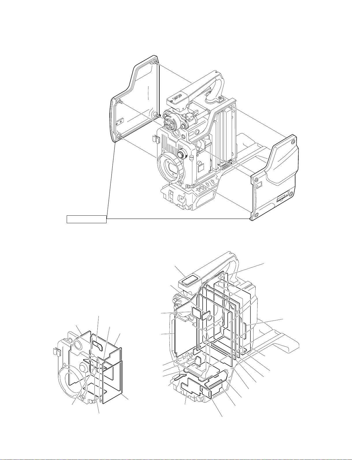
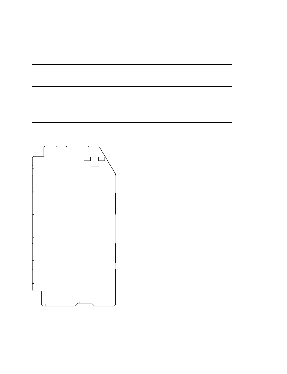
1-5. Remove and Installation of Exterior Parts
Loosen 4 screws.
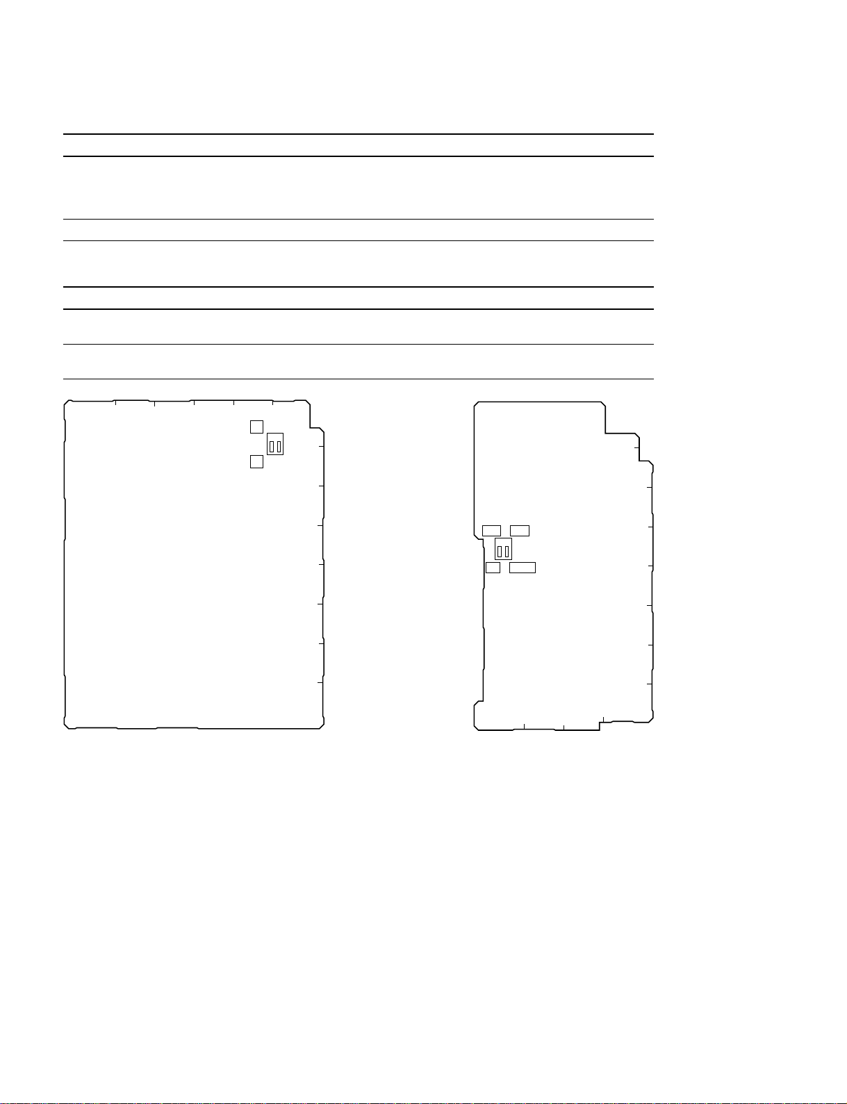
1-6. Location of Printed Wiring Boards
SW-1075
SW-1071
TG-229
PA-272
SE-767
(BVP-E30P only)
PA-273
NR-72
PA-274
CN-2209
DPR-261
CN-2210
CN-2208
CN-2205
CN-2207
DR-536
(BVP-E30/E30WS/
E30WSP only)
SW-1068
MB-953
CN-2204
DC-DC CONVERTER
(RE-201 board)
CN-2206
AT-148
IF-969
VA-226
SW-1067
SW-1069
SW-1070
BVP-E30/E30P M-V1
1-9 (E)

1-7. Circuit Description
1-7-1. CCD Block (PA-272/273/274 Boards,
TG-229 Board, and NR-72 Board)
PA-272/273/274 Boards
The PA boards contains the CCD bias circuit, horizontal
register drive circuit (H1, H2, LH1 driver), CDS (Correlated Double Sampling) circuit which extracts video signals
from the CCD and eliminates noise, and preamp circuit
which adjusts sensitivity.
IC9 of PA-273 board detects temperature around the CCD
block with a temperature sensor, and sends the detected
signal to the AT-148 board.
Various CCD drive conditions, adjustment data (V-sub
voltage, RG voltage, black/white shading, etc.) are written
in IC8 (EEPROM) of PA-272 board.
TG-229 Board
The TG-229 board contains the CCD drive pulse generation circuit and its drive circuit.
The 18 MHz clock generated from the voltage control
generation circuit (X1) is sent to the DPR-261 board to
generate the AHD, AVD pulse synchronized with the
video output signal.
The TG IC (IC1) generates the CCD drive pulse synchronized with this AHD, AVD pulse and the sample and hold
pulse for the CDS circuit of the PA boards.
These pulses are passed through the following drive circuit
and are sent to each PA board.
. V clock: Passed through IC201 to IC206 drivers ICs
. RG pulse: Passed through IC309 and then the bias
potential specific to each. CCD is added to the
output of IC309.
. V-sub voltage:
Enters IC310 DC amplifier to be adjusted for
the specified voltage.
. Shutter pulse:
Passes through the drive circuit consisting of
Q201 to Q204.
. SHP/SHD/H1/H2/LH1:
Passes through IC312, IC313, and IC307
AND gate ICs.
NR-72 Board
The NR-72 board contains a power stabilization circuit to
stabilize various power supply voltages to be supplied to
the CCD block, black/white shading correction signal
generation circuit, and optical filter interface circuits.
. The power stabilization circuit stabilizes the following
power supply voltages to be supplied to the CCD block.
+15.0 V +30.0 V +6.0 V +5.3 V +3.3 V +2.5 V
+1.8 V +1.1 V _10.0V _8.0 V _4.5 V
. The black/white shading correction signal and TEST
SAW signal are generated in IC104, and are sent to the
VA-226 board to mix with the video signal.
. This board has two optical filter interface circuits, one is
for the two-filters type with a servomotor used in the
BVP-E30/E30WS/E30WSP, the other is for one filter
type without a servomotor used in the BVP-E30P.
The switch S101 switches these circuits.
1-10 (E)
BVP-E30/E30P M-V1

1-7-2. Video Signal System (VA-226 Board,
DPR-261 Board, and IF-969 Board)
VA-226 Board
The VA-226 circuit amplifies the R, G, B video signals
output from the PA boards, performs various correction,
and then sends them to the DPR-261 board. As the R, G,
and B circuits are basically the same, Rch is explained as
an example below.
The video signal output from the PA board is passed
through the trap filter (FL101), and input to the first
amplifier stage composed of Q102 to Q108. In this amplifier, black shading correction, 5600K switching (Rch and
Bch only) and clamping are performed.
The clamped signal is switched between 0 dB/6 dB/12 dB/
18 dB by the amplifier composed of Q110 to Q117 and
blanking cleaning is performed by IC102. Clamping is also
performed in this amplifier.
After this, the change of 0 dB/3 dB/6 dB/12 dB and flare
correction are performed in the amplifier composed of
Q125 to Q131 and Q133 to Q135, and the signals are
output to the DPR-261 board.
In addition, switching of the video signal and TEST SAW
signal is also performed.
DPR-261 Board
The DPR-261 board is mainly composed of the A/D block
which converts analog RGB signals input from the VA226 board to digital, camera DSP (digital signal processor)
block which performs various signal processing, and D/A
block which converts digital signals processed by the
camera DSP block to analog.
In the A/D block, after analog RGB signals input from the
VA-226 board are clamped, they are passed through the
pre-filters (FL101, FL102, and FL103), and converted to
14-bit digital signals by the A/D converter (IC102, IC202,
and IC302).
The A/D-converted digital signals are input to the camera
DSP LSI (IC1).
IC1 performs detection of average values and peak values
of video signals required for automatic operations of the
camera such as auto black balance, auto white balance,
auto iris, etc., processings white balance, white shading
correction, matrix, detail, and gamma, and digital encoding
for VBS signals. 25 PsF/29.94 PsF conversion functions
and slow shutter are also realized using the SDRAM
(IC801). These processed signals are output from IC1 as
various digital video signals.
Of the digital video signals output from IC1, only the Y/RY/B-Y signals for the digital CA are passed through the
buffers (IC1001 to IC1005) and then output at the DPR261 board as the digital signals. The other digital signals
are converted to analog signal.
In the D/A block, the Y/R-Y/B-Y signal is D/A-converted
by IC501, the VBS/SC by IC502, the Y/R-Y/B-Y signal
for VF by IC503, and the TEST signal by IC800.
The DPR-261 board, also control PLL and H-Phase/SCPhase at genlock and generates various timing pulses such
as HD/VD/SYNC.
BVP-E30/E30P M-V1
1-11 (E)

IF-969 Board
The IF-969 board is composed of the driver block which
switches and outputs the analog signals D/A converted by
the DPR-261 board and RET signal sent when CCU is
connected to each block, and the I/O block inputs/outputs
the control signals from/to the lens, VF and the camera
adaptor.
The VBS signal which is D/A-converted by the DPR-261
board is input to the IF-969 board and branched into two.
One is sent to the camera adaptor as VBS output by 75 Z
output driver after passed through the video driver IC
(IC105). The other is switched by the analog switch IC
(IC104) and output at the TEST OUT terminal.
This unit has the two systems to output the TEST signal.
One system outputs the TEST signal as a MONITOR OUT
to the camera adapter after being switched by IC104
analog switch.
The other outputs that at the TEST OUT terminal by the
75 Z output driver after passing through IC105 driver IC.
At this terminal, VBS, TEST or RET signals which is
selected by IC104 analog switch is output. According to
another switch setting, character signal can be added to the
above output signal.
The RET signal sent when CCU is connected and the
GENLOCK input signal from the camera adaptor are
switched by the analog switch circuit (Q101 to Q107) and
the RET signal is separated to two pathes. The one is
output at the TEST OUT terminal via the analog switch IC
(IC104) after switching between the RET signal and the
TEST signal is done by the analog switch circuit (Q126,
Q115 to Q117, IC2). The other is output to VF VIDEO
OUT after switching between the RET signal and the VFVIDEO signal is done by the analog switch circuit (Q4 to
Q6).
To synchronize the GENLOCK input of the camera
adaptor with the external input video signal, the IF-969
board is provided with the floating amplifier circuit and
sync separation circuit to send the external sync signals
EXT-SC and EXT-SYNC to the DPR-261 board.
When a color VF is connected, the signals VF-Y, VF R-Y,
VF B-Y input from the DPR-261 board are mixed with the
cursor, marker signal and character signal generated in the
character generator IC (IC5) and then output as a COLOR
VF signal.
When a white/black VF is connected, the VF-Y signal
input from the DPR-261 board are mixed with the cursor,
marker and character signals in the different block to the
COLOR VF signal and then output to VF VIDEO OUT as
a monochrome VF signal.
The I/O block controls the switching input signal from the
switches of the camera, input/output signals from/to the
camera adaptor and lens, and output signal to VF using the
I/O expander (IC307) which communicates with the AT148 board.
1-7-3. System Control (AT-148 Board)
AT-148 Board
The AT-148 board is provided with a CPU (IC11) which
performs system control.
It is operated by the program written in the ROM (IC231
and IC232). The program can be upgraded using a memory
stick via the controller IC222.
The AT-148 board is also provided with a general memory
SRAM (IC216 and IC217) and FRAM (IC220 and IC221)
for recording system setting conditions, etc.
The external 8-bit bus (IC205, IC206, IC207, and IC208)
controls the I/O expander (IC307) of the IF-969 board and
the digital signal processor LSI (IC1). It also controls IC1
of the TG-229 board, IC104 of the NR-72 board, D/A
converter of the VA-226 board (IC702 and IC704), D/A
converter of the DPR-261 board, and switch input (IC1001
and IC1002) of the CN-2205 board by serial communication.
The A/D converter of the CPU reads the IRIS, ZOOM, and
EXTENDER signals from the lens, and controls the lens
via the channel B of the communication IC (IC224).
In additional the CPU performs temperature control using
the temperature sensor signal of channel G sent from the
CCD block (PA-273 board), position control from the filter
block, tape remainder control, and audio volume control.
It is also provided with the serial I/O which communicates
with the CCU using the 700 protocol (channel A of IC224)
and the calendar function (IC3).
1-12 (E)
BVP-E30/E30P M-V1

1-7-4. Power Supply Block (DC-DC
Converter) (RE-201 Board)
RE-201 Board
. The RE-201 board is a DC-DC converter which outputs
11 types of voltages altogether.
. PWM Clock Signal
The PWM POWER CONTROL (IC8) generates and
supplies the master clock (triangular wave of 90 ±10
kHz) for all controller ICs (IC2, IC3, IC7, and IC8) .
. Input Voltage Monitoring Circuit
The RE-201 board has an input voltage monitoring
circuit (IC4). If the voltage is within the appropriate
range, it supplies power to each controller IC (IC2, IC3,
IC7, and IC8) and REF voltage IC (IC1).
The power supply circuit starts up when the input power
voltage is within the range of +10.0 V to +18.8 V. Once
it has started up, the circuit keeps operating until the
input power voltage decreases below the lower limit
(+9.4 V).
. Voltage Control Circuit
The eight output voltages out of the 11 voltages are
stabilized with direct feedback control by the PWM
POWER CONTROL (IC2, IC3, IC7, and IC8). Each
control IC can independently control two voltages each.
+1.4 V, +2.5 V, +5.3 V, +3.3 V, +6.6 V, and +9.3 V
are output from the step-down chopper circuit while
_5 V is output from the polarity reversed chopper
circuit. The sync rectification circuit is adopted for all
except +9.3V to obtain high efficiency.
_10.5 V is output from the flyback regulator using the
transformer T1. The three voltages +16.0 V, +32.0 V,
and +46.0 V are also output by the T1 coil, however
they are not directly stabilized.
For +1.4 V, accurate voltage is required.
Therefore, it detects the voltage in the DPR-261 board to
absorb voltage drop during transmission.
. Protection Circuit for Shorting of Output Circuit
Each output is connected with a diode or transistor. In
normal operations, they are reverse-biased so that they
are turned OFF.
However if any single output is shorted, or if there is no
output due to some defect, the diode and transistor of the
corresponding block are turned ON and IC9 sends a
L_SHUTDOWN signal. The master clock is stopped by
this signal, and the outputs of all voltages stop.
. Output Overvoltage Protection Circuit
An overvoltage detection circuit is equipped only for the
+1.4 V output.
When the +1.4 V output exceeds +2.0 V under abnormal conditions, the outputs of all voltages are stopped by
the L_SHUTDOWN signal like the output short-circuit
protection circuit.
BVP-E30/E30P M-V1
1-13 (E)
1-8. Diagnosis
The unit is provided with the diagnosis function which can be used for the self-diagnosis of each plug-in
board and the OHB, and is displayed in the OPERATION menu.
Operation
Display the “DIAGNOSIS” page of the OPERATION menu referring to Section 3-1.
Display
<DIAGNOSIS>
ROM:V1.00
CAMERA:UC CA-570
1
3
4
5
6
7
Description on display
OHB:-- MD:- VA :-- AU:--
2
DPR:-- TR:- IF :- AT :- HUR:99999H
CCU :--
8
Marks Board/Block Criteria for judging
1 OHB (CCD UNIT) Communication error with IC8/PA-272 board
2 VA-226 Communication error with IC701 or defect of sub-regulator circuit operation inside the
3 DPR-261 Communication error with IC507 or defect of sub-regulator circuit operation inside the
4 IF-969 Communication error with IC307 or defect of sub-regulator circuit operation inside the
5 AT-148 Low capacity of BT1
6 HUR Indicates the power-on time of the camera. (The display stops in 99999 when the
7 CCU/RM
* When neither CCU nor RM is connected, “RM: NC” is displays.
*
board.
board.
board.
power-on time exceeds 99999H.)
The serial data is correctly received from the CCU or RM connected to the unit.
(“__” is displayed during a normal operation.)
About mark 8 CA, is as described below according to the type of CA connected to the camera.
Refer to the maintenance manual supplied with the camera adaptor.
CA-570 CA-550
MD:-- MD:- AU:-- AU:- TR:-- TR:--
CA-530 CA-950
VSE:-- DA :- DVP:-- IF :- DC :-- AU :- SDI:- DPR:- TX :--
1-14 (E)
BVP-E30/E30P M-V1

1-9. Contents of the EEPROM and FRAM Data
The data that is stored in the EEPROM and FRAM on the respective boards, is shown below.
n
Part numbers of the following ICs are shown in Vol. 2 Section “1. Spare Parts” of the separate Maintenance Manual are the ICs before saving the data contents.
Board Ref. No. EEPROM/ Contents of the saved data Adjustment/setup upon
AT-148 IC220 FRAM Reference file setting data Refer to Section 1-10-7.
DPR-261 IC507 EEPROM Factory adjustment data of Refer to Section 1-10-6.
PA-272 IC8 EEPROM Factory adjustment data of *1
VA-226 IC701 EEPROM Factory adjustment data of Refer to Section 1-10-5.
*1: IC8 on the PA-272 board cannot be replaced because the data cannot be re-set.
When IC needs to be replaced due to defective IC, contact your local Sony Sales Office/Service Center.
(address) FRAM replacement of EEPROM/FRAM
(A-2/A side) Scene file setting data
IC221 Lens file setting data
(A-3/A side) Operator file setting data
VF menu setting data
(F-10/A side) DPR-261 board
(except SC Frequency data)
(B-1/B side) CCD block
SC Frequency data
(D-12/A side) VA-226 board
BVP-E30/E30P M-V1
1-15 (E)

1-10. Adjustment and Setting Items After
Replacement of Board
When replacing the following boards, perform the adjustments or settings referring to Section 5 “Electrical Alignment”
If no adjustment item is listed, no adjustment is required.
Board Referring section
CCD unit 1-10-1. CCD Unit
TG-229 board 1-10-2. TG-229 Board
NR-72 board 1-10-3. NR-72 Board
VA-226 board 1-10-4. VA-226 Board
DPR-261 board 1-10-5. DPR-261 Board
AT-148 board 1-10-6. AT-148 Board
1-10-1. CCD Unit
1-10-4. VA-226 Board
The EEPROM (IC701) is mounted on the VA-226 board.
Perform the following adjustments, when this IC is
replaced, too.
Adjustment Items After Board or EEPROM is
Replaced
5-2-1. Black Balance Adjustment
5-2-2. Offset Adjustment
5-2-3. Flare Offset Adjustment
1-10-5. DPR-261 Board
The EEPROM (IC507) is mounted on the DPR-261 board.
Perform the following adjustments, when this IC is
replaced, too.
Adjustment and Setting Items After CCD Unit is
Replaced
5-3-1. PA Gain Adjustment
5-4-3. SC Frequency Adjustment
4-7. OHB file (Adjustment and Saving the OHB file)
1-10-2. TG-229 Board
Setting Items After Board is Replaced
Referring to Section 1-4, set the internal switches.
1-10-3. NR-72 Board
Setting Items After Board is Replaced
Referring to Section 1-4, set the internal switch.
Adjustment Items After Board or EEPROM is
Replaced
5-4-1. Video Level Adjustment
5-4-2. TEST OUT Level Adjustment
1-10-6. AT-148 Board
The unique setting data that is set by user is written into
IC220 and IC221 on the AT-148 board.
Therefore, when these ICs were replaced with new ICs in
replacing the board or IC itself, the data set by user is lost,
and is returned to their factory-setting values.
Perform the following settings, when these ICs are replaced, too.
Setting Items After Board or FRAM is Replaced
. Reset the reference file, operator file and scene file.
(Refer to Section 4.)
. Replace lithium battery on the AT-148 board with a new
one, and reset date. (Refer to Sections 1-1-5 and 3-5.)
1-16 (E)
BVP-E30/E30P M-V1

1-11. Upgrading the Software
The version of the MAIN program and BOOT program can
be upgraded using the memory stick. According to necessary, follow the procedures shown below.
m
. The upgrading program must have already been saved in
a memory stick before.
. Refer to Section 5-1-6 to display of the SERVICE menu.
. Refer to Section 3-1 for the basic operations of the setup
menu.
1-11-1. Upgrading MAIN Program
When the Setup Menu is Used for Version
Upgrading
1. Insert the memory stick in which the upgrading
program is already saved.
2. Display the FIRM UPDATE page of the SERVICE
menu, and execute the MAIN PROGRAM.
3. The upgrading status is displayed on the viewfinder
screen.
4. When the version upgrade is completed, the message
“Complete” will be displayed.
n
When the tally switch on the camera adaptor is set to
ON, the tally lamp will blink during being upgrading,
and then light up when upgrading is completed.
5. Restart the unit, and confirm the version indication
using DIAGNOSIS menu.
Upgrading by Powering ON the Unit
1. Insert the memory stick in which the upgrading
program is already saved.
2. Turn on the power while pressing the VTR START
switch and MENU SELECT knob on the camera front
simultaneously.
3. The upgrading status is displayed on the viewfinder
screen.
4. When the version upgrade is completed, the message
“Complete” will be displayed.
n
When the tally switch on the camera adaptor is set to
ON, the tally lamp will blink during being upgrading,
and then light up when upgrading is completed.
5. Restart the unit, and confirm the version indication
using DIAGNOSIS menu.
1-11-2. Upgrading BOOT Program
BOOT program is a software renewing the firmware using
the memory stick. Do not operate this program except
upgrading the program.
1. Insert the memory stick in which the upgrading
program is already saved.
2. Display the FIRM UPDATE page of the SERVICE
menu, and execute the BOOT PROGRAM.
3. When the version upgrade is completed, the message
“Complete” will be displayed.
n
When the tally switch on the camera adaptor is set to
ON, the tally lamp will blink during being upgrading,
and then light up when upgrading is completed.
BVP-E30/E30P M-V1
1-17 (E)

1-12. Setting Scene File Number
The number of scene files that can be registered can be
changed (to 5 or 32) using the SERVICE menu of this unit.
The number of scene files can be stored in the internal
memory of this unit, memory stick, and IC memory card
(when MSU is used).
However, pay attention to the following when changing the
number of scene files again after it is changed.
When the number of scene files is switched from
5 to 32:
Indefinite data is registered in the values of scene files 6 to
32. Be sure to register new data again before using the
scene files.
When the number of scene files is switched from
32 to 5:
The data registered in scene files 6 to 32 is deleted. The
deleted data cannot be restored.
m
. This setting corresponds only to MSU-700A/750 and
RCP-730 series.
. Each scene file have no compatibility among the camer-
as if their scene file number differs.
How to change
Change the scene file number using the SETUP page in the
SERVICE menu.
Refer to Section 5-1-6 to display of the SERVICE menu.
Menu setting:
MENU: SERVICE
PAGE: SETUP
ITEM: SCENE FILE TYPE → 5 or 32
1-18 (E)
BVP-E30/E30P M-V1
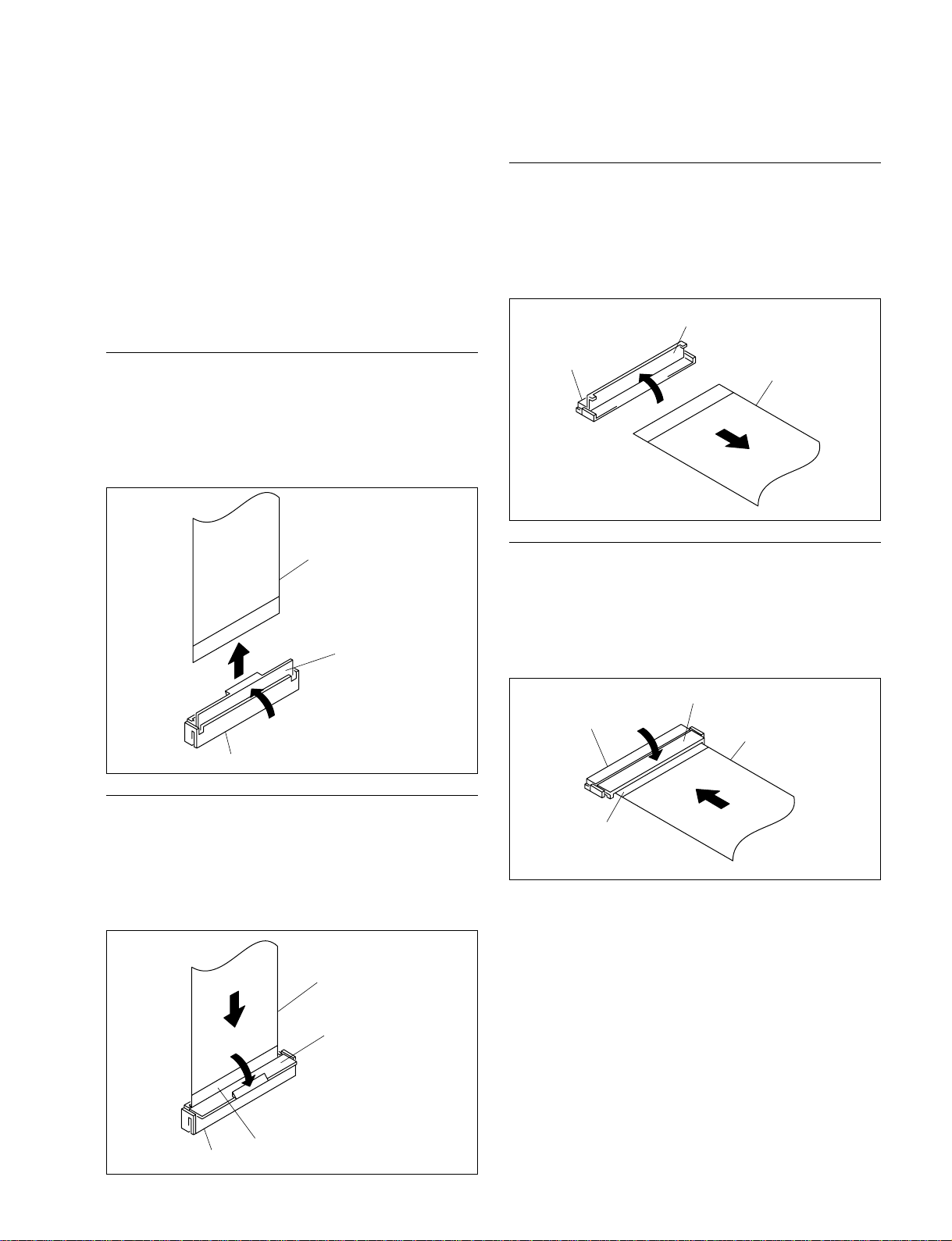
1-13. Removing and Reinstalling the
Flexible Card Wires
This unit uses two types of flexible card wire.
n
Life of flexible card wire will be significantly shortened if
it is folded. Be very careful not to fold the flexible card
wire.
Type-B
Removal
1. Open the connector latch in the direction of arrow A to
release the lock.
2. Remove the flexible card wire in the direction of arrow
B.
Type-A
Removal
1. Open the connector latch in the direction of arrow A to
release the lock.
2. Remove the flexible card wire in the direction of arrow
B.
Flexible card wire
B
A
Connector
Connector latch
Reinstallation
1. Hold the flexible card wire with its blue surface facing
to the front, and insert it in the direction of arrow A.
2. Close the connector latch in the direction of arrow B to
lock it.
Connector latch
Connector
A
Flexible card wire
B
Reinstallation
1. Hold the flexible card wire with its blue surface facing
upward, and insert it in the direction of arrow A.
2. Close the connector latch in the direction of arrow B to
lock it.
Connector latch
Connector
B
Blue surface
Flexible card wire
A
Connector
BVP-E30/E30P M-V1
A
B
Blue surface
Flexible card wire
Connector latch
1-19 (E)
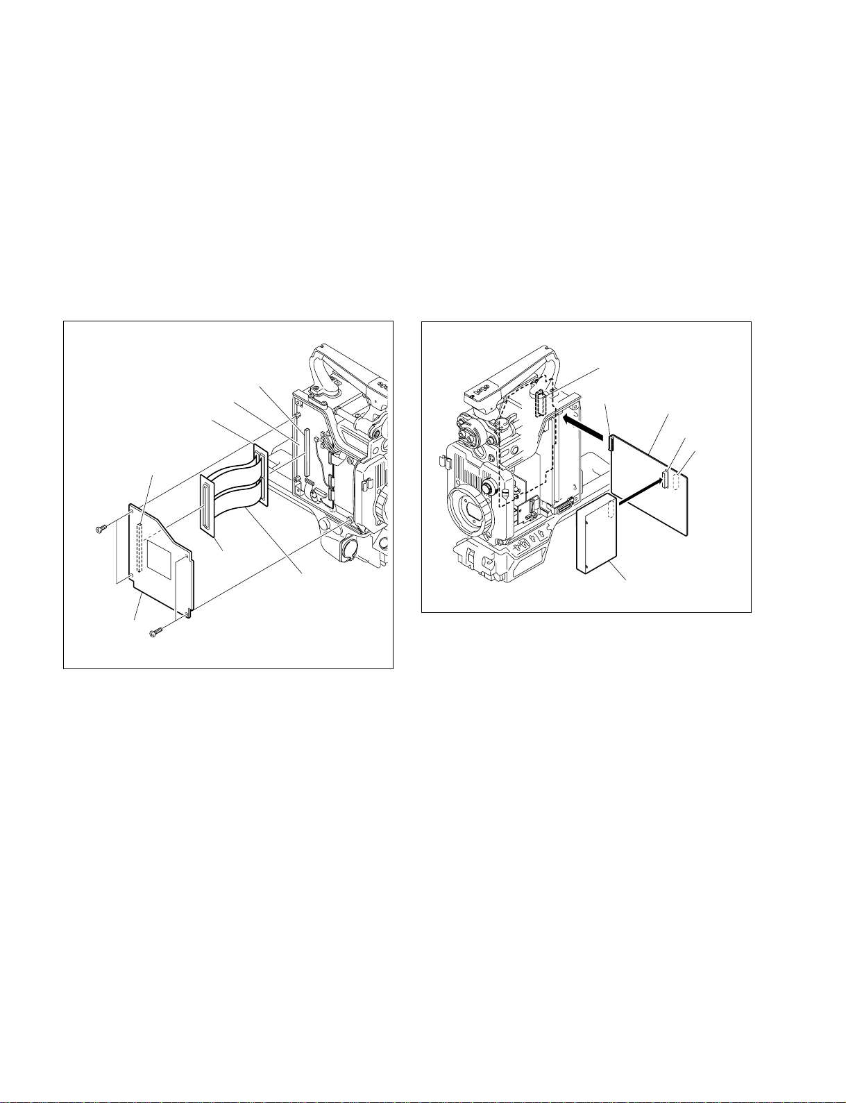
1-14. How to Extend the Circuit Board
1-14-2. Extending the DC-DC Converter
1-14-1. Extending the DPR-261 Board
Tool: DPR-261 board extension assembly
1. Remove the left side panel. (Refer to Section 1-5.)
2. Remove the four screws, and remove the DPR-261
board.
3. Extend the DPR-261 board as shown below using the
DPR-261 board extension assembly.
CN13
MB-953 board
EX-884 board side
CN1
B2.6 x 5
Tool: EX-878 Board
1. Remove the right side panel. (Refer to Section 1-5.)
2. Remove the DC-DC converter (RE-201 board). (Refer
to Section 2-12.)
3. Connect the connector CN1 on the EX-878 board to
the connector CN10 on the MB-953 board.
4. Connect the DC-DC converter to the connector CN2 or
CN3 on the EX-878 board.
CN10/MB-953 board
CN1
EX-878 board
CN2
CN3
DPR-261
board
B2.6 x 5
EX-885
board side
DPR-261 board
extension assembly
DC-DC converter
1-20 (E)
BVP-E30/E30P M-V1
 Loading...