

Page 1
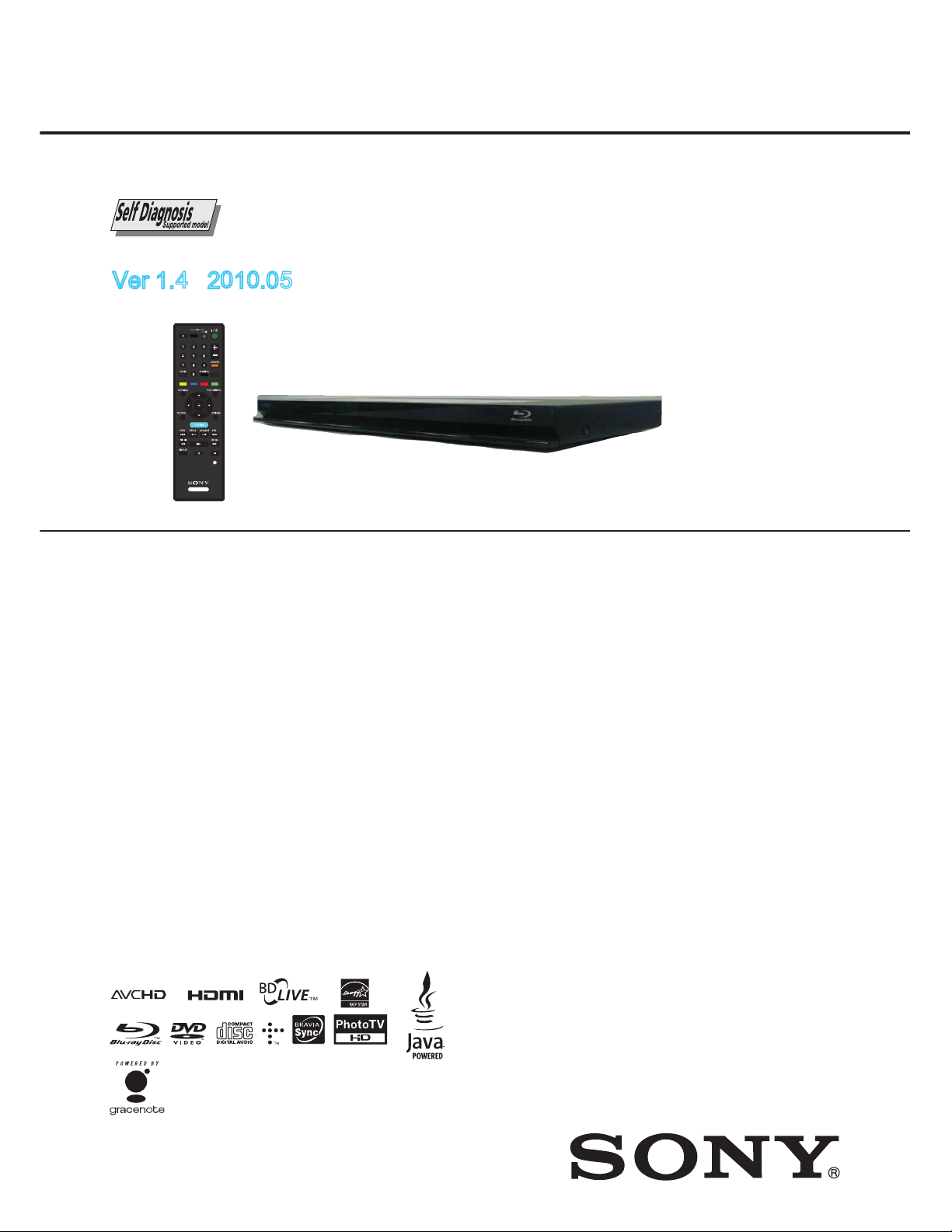
BDP-BX37/S270/S370/S373/S47
0
RMT-B107A/RMT-107P/RMT-107C/RMT-108A/RMT-108P
SERVICE MANUAL
BDP-BX37/S270/S370/S470
Ver 1.4 2010.05
4
OPEN/
CLOSE
INPUT
FAVORITES
T
Y
/
/
PLAY
STOP
PAUSE
LIGHT
BD
RMT-B107P
System
Laser: Semiconductor laser
Inputs and outputs
(Jack name:
Jack type/Output level/Load impedance)
LINE OUT R-AUDIO-L:
Phono jack/2 Vrms/10 kilohms
DIGIT AL OUT (OPTICAL):
Optical output jack/-18 dBm
(wave length 660 nm)
DIGIT AL OUT (COAXIAL):
Phono jack/0.5 Vp-p/75 ohms
HDMI OUT:
HDMI 19-pin standard connector
COMPONENT VIDEO OUT (Y , P
Phono jack/Y: 1.0 Vp-p/
P
B, PR: 0.7 Vp-p/75 ohms
LINE OUT VIDEO:
Phono jack/1.0 Vp-p/75 ohms
LAN (100):
100BASE-TX T erminal
USB:
USB jack Type A ( For connecting a USB
memory, memory card reader, digital stil
camera, and digital video camera)
BDP-S270: USB-023(REAR USB)
BDP-BX37/S370/S373/S470:
TM
5
Australian / New Zealand Model
Photo: BDP-S370
SPECIFICA TIONS
, PR):
B
FR-309(FRONT USB)/
USB-023(REAR USB)
Canada Model
Argentina Model
US Model
Mexican Model
BDP-S270
Brazilian Model
BDP-S270/S370/S470
Chinese Model
Middle East Model
Russian Model
Saudi Arabia Model
PX Model
BDP-S370
Singapore Model
Taiwan Model
Thailand Model
General
Power requirements:
120 V A
220-240 V AC, 50/60 Hz
110-240 V AC, 50/60 Hz
120 V A
220 V AC, 6 0 H z (BDP-S370:KR/S470:KR only)
110 V A
P ower consumption:
Dimensions (approx.):
430 mm × 219 mm × 36 mm
(17 in. × 8
(width/depth/height) incl. projecting parts
Mass (approx.):
2.0 kg (4 lb 6
Operating temperature:
5 °C to 35 °C (41 °F to 95 °F)
Operating humidity:
25 % to 80 %
Supplied accessories
J Audio/video cable (phono plug × 3) (1)
HDMI Cable :BDP-BX37:US/S270:MX/S370:AR/S470:E,AR,BR
J
Plug Adaptor :BDP-S370:PX,E/S470:E
J
J
Remote commander (remote) (1)
J
Size AA (R6) Batteries (2)
Specifi cations and design are subject to change
without notice.
ENERGY STAR an d t he ENERGY STAR ma r k
ar e regi ster ed U.S. mark s. EN ERGY STAR i s a
registered mark owned by the U.S. govern ment.
(BDP-BX37/S270/S370/S470: US Only)
C, 60 Hz
(BDP-BX37/S270/S370/S470:US,CND only)
(BDP-S370:UK,AE1,AE2,AUS,RUS,CN/S373/S470:UK,AE1,AE2AUS,RUS,CN)
(BDP-S270:BR/S370:PX,E,AR,BR,SP,TH,EA,KS/S470:E,AR,BR,SP,TH,EA,KS)
C, 50/60 Hz (BDP-S270:MX only)
C, 60 Hz (BDP-S370:TW/S470:TW only)
18 W (BDP-S270)
22 W (BDP-BX37/S370/S373/S470)
7
5
/8
Exce pt : BDP-S270:MX,BR/ S370:E,BR,UK,AE1,AE2,AR/
in.)
in. × 1
/
16
1
/
oz)
2
S373:UK,AE1,AE2/S470:E,AR,BR,AE1,AE2,UK
E Model
EA Model
Korea Model
BDP-S370/S470
AEP Model
UK Model
BDP-S370/S373/S470
9-890-726-15
BLU-RA Y DISC/DVD PLA YER
Sony Corporation
Home Entertainment Business Group
2010E6900-1
Published by Design Engineering Dept.
© 2010.05
Page 2
BDP-BX37/S270 /S370/S37 3/S470
SAFETY CHECK-OUT
After correcting the original service problem, perform the following
safety checks before releasing the set to the customer:
1. Check the area of your repair for unsoldered or poorly-soldered
connections. Check the entire board surface for solder splashes
and bridges.
2. Check the interboard wiring to ensure that no wires are “pinched”
or contact high-wattage resistors.
3. Look for unauthorized replacement parts, particularly transistors,
that were installed during a previous repair. Point them out to
the customer and recommend their replacement.
4. Look for parts which, though functioning, show obvious signs
of deterioration. Point them out to the customer and recommend
their replacement.
5. Check the line cord for cracks and abrasion. Recommend the
replacement of any such line cord to the customer.
6. Check the B+ voltage to see it is at the values specified.
7. Check the antenna terminals, metal trim, “metallized” knobs,
screws, and all other exposed metal parts for AC leakage. Check
leakage as described below.
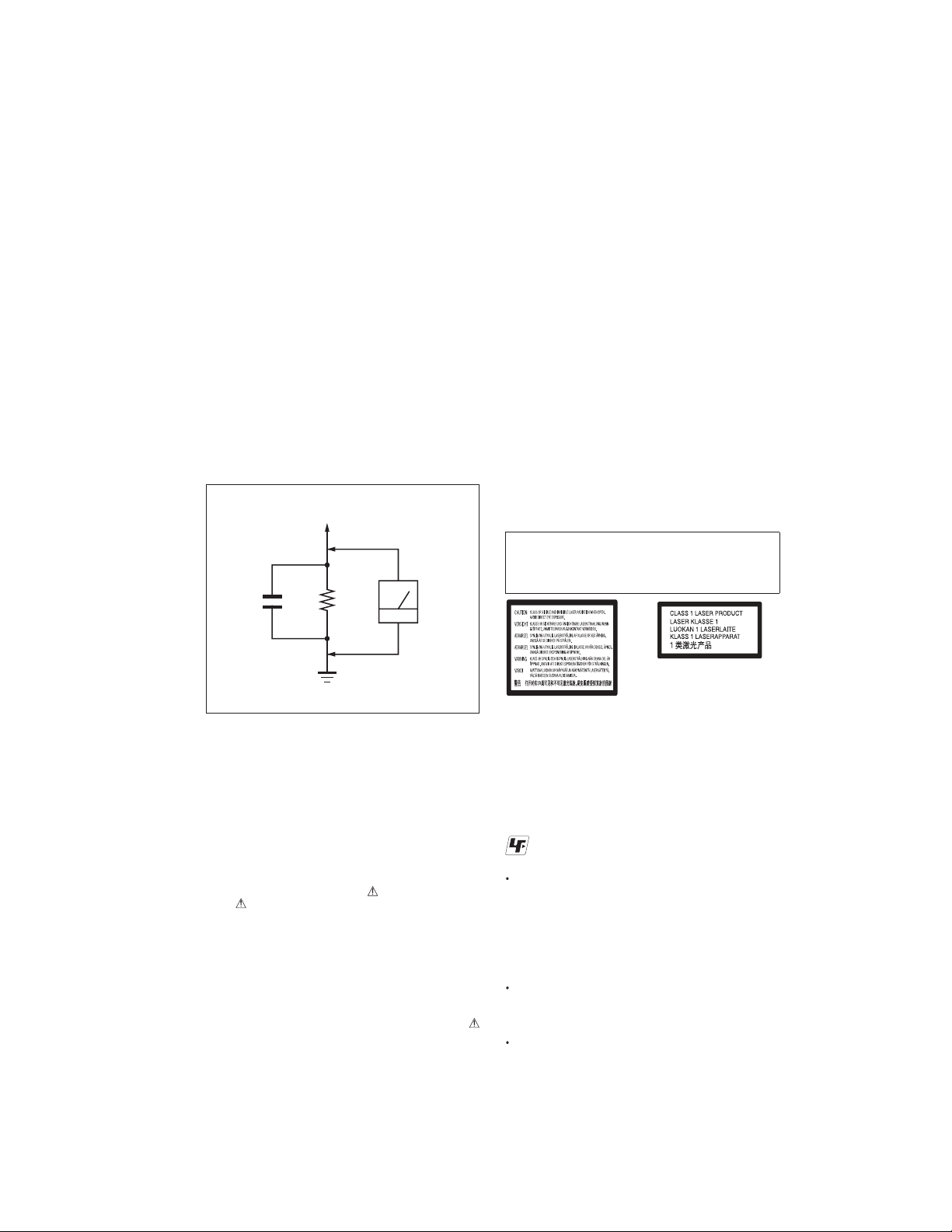
To Exposed Metal
Parts on Set
AC
1.5 k0.15 F
Earth Ground
Fig. A. Using an AC voltmeter to check AC leakage.
voltmeter
(0.75 V)
W ARNING!!
WHEN SERVICING, DO NOT APPROACH THE L ASER
EXIT WITH THE EYE TOO CLOSELY. IN CASE IT IS
NECESSARY TO CONFIRM LA SER BEAM EMISSI ON,
BE SURE TO OBSERVE FROM A DISTANCE OF MORE
THAN 25 cm FROM THE SURFACE OF THE OBJECTIVE
LENS ON THE OPTICAL PICK-UP BLOCK.
SAFETY-RELA TED COMPONENT WARNING!!
COMPONENTS IDENTIFIED BY MARK
MARK
ON THE SCHEMA TIC DIAGRAMS AND IN THE PARTS
LIST ARE CRITICAL TO SAFE OPERATION. REPLACE THESE
COMPONENTS WITH SONY PARTS WHOSE PART NUMBERS
APPEAR AS SHOWN IN THIS MANUAL OR IN SUPPLEMENTS
PUBLISHED BY SONY .
ATTENTION AU COMPOSANT AY ANT RAPPORT
LES COMPOSANTS IDENTIFIÉS PAR UNE MARQUE
SUR LES DIAGRAMMES SCHÉMATIQUES ET LA LISTE
DES PIÈCES SONT CRITIQUES POUR LA SÉCURITÉ DE
FONCTIONNEMENT. NE REMPLA CER CES COMPOSANTS
QUE PAR DES P IÈC ES SONY DON T LE S NUMÉR OS SONT
DONNÉS DANS CE MANUEL OU DANS L ES SUPPLÉMENTS
PUBLIÉS PAR SONY.
À LA SÉCURITÉ!
OR DOTTED LINE WITH
LEAKAGE TEST
The AC leakage from any exposed metal part to earth ground and
from all exposed metal parts to any exposed metal part having a
return to chassis, must not exceed 0.5 mA (500 microamperes).
Leakage current can be measured by any one of three methods.
1. A commercial leakage tester , such as the Simpson 229 or RCA
WT-540A. Follow the manufacturers' instructions to use these
instruments.
2. A battery-operated AC milliammeter. The Data Precision 245
digital multimeter is suitable for this job.
3. Measuring the voltage drop across a resistor by means of a
VOM or battery-operated AC voltmeter . The “limit” indication
is 0.75V, so analog meters must have an accurate low-voltage
scale. The Simpson 250 and Sanwa SH-63Trd are examples
of a passive VOM that is suitable. Nearly all battery operated
digital multimeters that have a 2V AC range are suitable. (See
Fig. A)
CAUTION:
The use of optical instrument with this product will increase eye
hazard.
CAUTION
Use of controls or adjustments or performance of procedures
other than those specified herein may result in hazardous radiation exposure.
This appliance is classied as a
CLASS 1 LASER product. The
CLASS 1 LASER PRODUCT
This label islocated on the laser
protective h ou sing insi de the
enclosure.
MARKING is located on the laser
protective housing inside the
enclosure. (AEP, UK, Australian
New Zealand)
Unleaded solder
Boards requiring use of unleaded solder are printed with the leadfree mark (LF) indicating the solder contains no lead.
(Caution: Some printed circuit boards may not come printed with
the lead free mark due to their particular size.)
: LEAD FREE MARK
Unleaded solder has the following characteristics.
Unleaded solder melts at a temperature about 40°C higher than
ordinary solder.
Ordinary soldering irons can be used but the iron tip has to be
applied to the solder joint for a slightly longer time.
Soldering irons using a temperature regulator should be set to
about 350°C.
Caution: The printed pattern (copper foil) may peel away if the
heated tip is applied for too long, so be careful!
Strong viscosity
Unleaded solder is more viscous (sticky, less prone to flow) than
ordinary solder so use caution not to let solder bridges occur such
as on IC pins, etc.
Usable with ordinary solder
It is best to use only unleaded solder but unleaded solder may
also be added to ordinary solder.
-2-
Page 3

BDP-BX37/S270/S370/S373/S470
TABLE OF CONTENTS
egaP eltiT noitceS egaP eltiT noitceS
1. SERVICE NOTE
1-1. Disc Removal Procedure If The Tray Cannot Be
Ejected (Forced Ejection) ............................................. 1-1
1-2. Work when optical device are replaced ........................ 1-1
1-3. Test Disc ....................................................................... 1-2
1-3-1. Operation and Display ............................................. 1-2
1-3-2. Main functions ......................................................... 1-9
1-4. Drive Repairing............................................................. 1-15
1-4-1. Preparation .............................................................. 1-15
1-4-2. Checking Flow ~ Drive (BU) section ~ .................... 1-15
1-4-3. BU Check Flow [zz] ~ .............................................. 1-16
1-4-4. BU (Optical Block) Repair Guide ............................. 1-16
1-4-5. BU Adjustment Flow [yy] ~ ...................................... 1-17
1-4-6. KEM-460AAA/C2RP Packing Spec. ....................... 1-17
1-4-7. KEM-460AAA/C2RP Packing .................................. 1-18
1-4-8. BU Data Decode Jig ................................................ 1-19
1-4-9.
1-4-10. Laser Caution Label ................................................ 1-20
1-5. Harness Dressing .........................................................
1-5-1.
1-5-2.
1-5-3.
1-5-4.
1-6. Power Cord Soldering Location ...................................
1-7. Remove PT Protection on MB-134
Loading For Service
Front harness dressing for S270 only
Front harness dressing for BX37/S370/S373:
AE1;UK;RUSSIAN;KOREAN;AUSTRALIA;
THAILAND;CHINA,SAUDI ARABIA and EA7 ONLY
Front USB(USB-008) and Harness(SIM-001)
dressing for BX37/S370/S373: US,CND,PX,
TAIWAN,E,BRAZILIAN and ARGENTINA ONLY
Rear USB and Harness dressing for BDP-BX37/
S270/S370/S373/S470
Rear USB (USB-007)
1-6-1. Soldering point for Switching Regulator (APS-257)....
1-6-2. Soldering point for Switching Regulator (SRV2206UC)
..................... 1-24
.........................................
.............................................
(Service Assy Main Board)...............
....
1-19
1-24
1-24
1-25
1-26
1-27
1-27
1-27
1-28E
2. DISASSEMBLY
2-1. Disassembly Flow ........................................................ 2-1
2-2. Upper Case .................................................................. 2-1
2-3. Tray Cover Assy .......................................................... 2-2
2-4. BD Drive ....................................................................... 2-2
2-5. Front Panel Assy, SWB-001 and SWP-001.................. 2-3
2-6. Rear Panel Block.......................................................... 2-4
2-7. MB-134 Board .............................................................. 2-4
2-8. Switching Regulator ..................................................... 2-5E
2-9. Circuit Boards Location ................................................ 2-5E
3. BLOCK DIAGRAMS
3-1. Overall Block Diagram.................................................. 3-1
3-2. DSP Block Diagram ...................................................... 3-2
3-3. AV OUT Block Diagram ................................................ 3-3
3-4. USB/ETHER, Block Diagram .................................. 3-4
3-5. Power Block Diagram .......................................... 3-5
4. SCHEMATIC DIAGRAMS
4-1. This Note Is Common For Schematic Diagrams .......... 4-1
4-2. Frame Schematic Diagram........................................... 4-2
4-3. FR-309 Board (FRONT RIGHT) Schematic Diagram ... 4-3
4-4. FR-309 Board (USB FRONT) Schematic Diagram ...... 4-4
4-5. MB-134 Board (CXD9983GG/9984GG)
Schematic Diagram (1/15)............................................ 4-5
4-6. MB-134 Board (CXD9983GG/9984GG)
Schematic Diagram (2/15)............................................ 4-6
4-7. MB-134 Board (POWER1)
Schematic Diagram (3/15)............................................ 4-7
4-8. MB-134 Board (CLK/POWER2)
Schematic Diagram (4/15)............................................ 4-8
4-9. MB-134 Board (FLASH/HOST)
Schematic Diagram (5/15)............................................ 4-9
4-10. MB-134 Board (USB) Schematic Diagram (6/15)......... 4-10
4-11. MB-134 Board (HDMI)
Schematic Diagram (7/15)............................................ 4-11
4-12. MB-134 Board (SATA)
Schematic Diagram (8/15)............................................ 4-12
4-13. MB-134 Board (AUDIO)
Schematic Diagram (9/15)............................................ 4-13
4-14. MB-134 Board (VIDEO)
Schematic Diagram (10/15).......................................... 4-14
4-15. MB-134 Board (GPIO/JTAG)
Schematic Diagram (11/15) .......................................... 4-15
4-16. MB-134 Board (ETHERNET)
Schematic Diagram (12/15).......................................... 4-16
4-17. MB-134 Board (FE_POWER/SF/SATA)
Schematic Diagram (13/15).......................................... 4-17
4-18. MB-134 Board (FE_OP/MOTOR DRIVE)
Schematic Diagram (14/15) ........................................ 4-18
4-19. MB-134 BOARD(IFD)
Schematic Diagram (15/15) ............................................ 4-19
4-20. SWB-001 BOARD
Schematic Diagram ...................................................... 4-20
4-21. SWP-001 BOARD
Schematic Diagram ...................................................... 4-20
4-22. USB-023 Board (REAR)
Schematic Diagram ...................................................... 4-21
4-23. Waveforms ................................................................... 4-22E
5. PRINTED WIRING BOARDS
5-1. This Note Is Common For Printed Wiring Boards ........ 5-1
5-2. SWB-001 Board (SWITCH) Printed Wiring Board........ 5-2
5-3. SWP-001 Board
Printed Wiring Board ...................................................... 5-2
5-4. FR-309 Board (FRONT RIGHT)
Printed Wiring Board ................................................... 5-3
5-5. MB-134 Board (MAIN)
Printed Wiring Board (Side A) ...................................... 5-4
5-6. MB-134 Board (MAIN)
Printed Wiring Board (Side B) ...................................... 5-5
5-7. USB-023 Board (REAR)
Printed Wiring Board .................................................... 5-6E
6. IC PIN FUNCTION DESCRIPTION ................... 6-1
7. SERVICE MODE ..................................................... 7-1
8. ERROR LOG LIST ................................................. 8-1
9. TROUBLESHOOTING ............................................. 9-1
10. REPAIR PARTS LIST
10-1. Exploded Views ............................................................ 10-1
10-1-1. Case Section ........................................................... 10-1
10-1-2. Front/Rear Chassis Section .................................... 10-2
10-1-3. Main Chassis Section .............................................. 10-3
10-1-4. BD Section .............................................................. 10-4
10-1-5. Accessories ............................................................. 10-5
10-2. Electrical Parts List ....................................................... 10-6
– 3 –
Page 4
BDP-BX37/S270/S370/S373/S470
SECTION 1
SERVICE NOTE
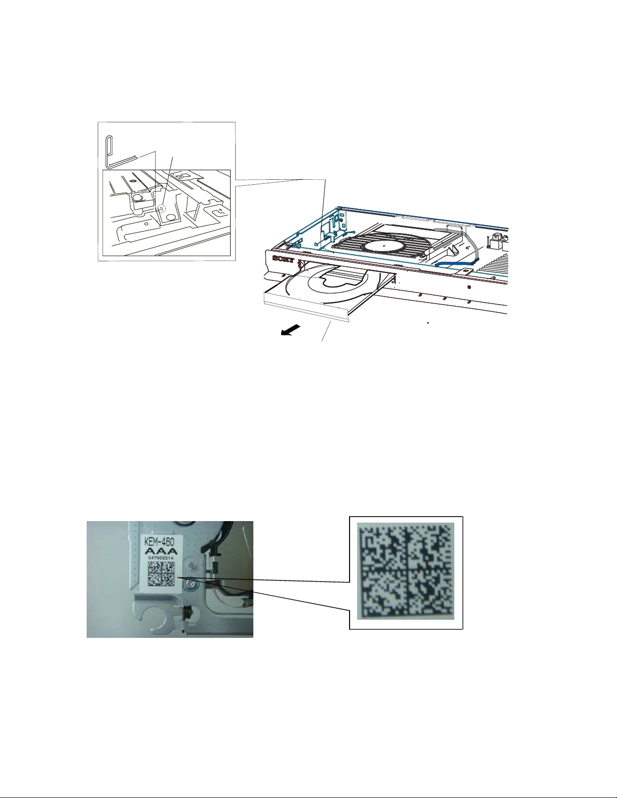
1-1. DISC REMOVAL PROCEDURE IF THE TRAY CANNOT BE EJECTED (FORCED EJECTION)
1. Remove the upper case. (Refer to page 2-1)
2. Insert a clip in the hole of a drive and open a tray.
Note:
(Use clip diameter about 1.2 mm)
(12~32)mm
clip
1-2. Work when optical device are replaced
Note:
Please do the following work when you replace the optical device.
1. Install it in PC after downloading two set of software from following URL.
(Refer to “1-4-9. BU Data Decode Jig” on page 1-19)
STEP 1
Microsoft .NET Framework Version 2.0 Redistributable Package (x86)
http://www.microsoft.com/downloads/details.aspx?displaylang=en&FamilyID=0856eacb-4362-4b0d-8edd-aab15c5e04f5
hole
Fig.1
tray
STEP 2
Microsoft .NET Framework 2.0 Service Pack 1 (x86)
http://www.microsoft.com/downloads/details.aspx?displaylang=en&FamilyID=79bc3b77-e02c-4ad3-aacf-a7633f706ba5
2. Take a photograph of the bar code on the optical device. The valid bar code photo as shown in Fig.2
3. Drag-and-drop the bar code photograph to the icon of decode software (BDBUDec).
* The decode software is a complete set of “BDBUDec”, “Tasman.Bars.dll”, and “SavePath”.
* Because decode software cannot be attached, it separately distributes it.
4. Input the password when you start decode software.
* Inquire of each service headquarters because the password cannot be disclosed.
5. Write the decode data to the set.
(Refer to “1-4-4. BU (Optical Block) Repair Guide” on page 1-16 and “1-4-5. BU Adjustment Flow [yy]” on page 1-17)
Fig.2
1-1
Page 5

BDP-BX37/S270/S370/S373/S470
1-3. TEST DISC
Part No. Description Layer
J-6090-199-A BLX-104 Single Layer
J-6090-200-A BLX-204 Dual Layer
J-2501-307-A CD (HLX-A1)
J-2501-305-A HLX-513 Single Layer (NTSC)
J-2501-306-A HLX-514 Dual Layer (NTSC)
J-6090-077-A HLX-506 Single Layer (PAL)
J-6090-078-A HLX-507 Dual Layer (PAL)
1-3-1. Operation and Display
Check Items
1) BLX-104
1. Select 23.976Hz/1080p
2. Play “4.Motion pictures”
3. Check whether player can play back or not
4. Check each outputs
Video:
Composite/component/HDMI
Audio:
Digital out (Coaxial/Optical)/Audio out/5.1Ch output
* When 1080/24p monitor is nothing, 1080i (59.94Hz or 50Hz) can use instead of 1080/24p.
However this is temporary correspondence.
2) BLX-204
1. Select 1080i (59.94Hz or 50Hz)
2. Play “4.Motion pictures”
3. Check whether player can play back or not
(Check the picture and sound output)
3) CD (HLX-A1)
Check whether player can play back or not
(Check the sound output)
4) HLX-513/514 (NTSC), HLX-506/507 (PAL)
1. After displayed Main Menu, select “1.Video”
2. Play “1.Color Bar 100%”
(Check the picture and sound output)
3. Return to Menu
4. Play “Demonstration 4:3” or “5.Demonstration 16:9”
(Check the picture and sound output)
1-2
Page 6
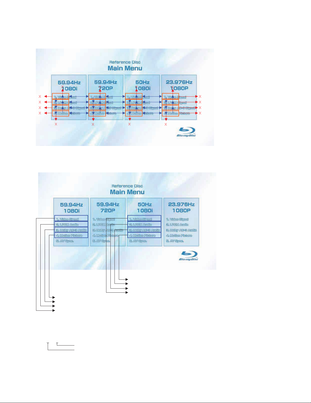
1-3-1-1. BLX-104 Menu Function (1)
Main Menu
BDP-BX37/S270/S370/S373/S470
X X X
X
X
X
X
X
X
X
X
X
X
X
X
X
1) When the disc is inserted, 1. Video Signal of 59.94Hz/1080i of the Main Menu is selectively displayed.
1-3-1-2. BLX-104 Menu Function (2)
Main Menu
To Main Menu after playback of T62_C1
To Main Menu after playback of T61_C1
To Main Menu after playback from T54_C1 to T60_C1
Sub_menu3 is displayed
To Main Menu after playback of T21_C1
To Main Menu after playback of T20_C1
To Main Menu after playback from T2_C1 to T19_C1
Sub_menu1 is displayed
* When returning to Main Menu after playback from each button of 59.94Hz/1080i, 1. Video Signal of 59.94Hz/1080i is selectively dis-
played.
* When returning to Main Menu after playback from each button of 50Hz/1080i, 1. Video Signal of 50Hz/1080i is selectively displayed.
* 5. AV Sync does not operate.
Note:
Txx_ Cxx
Chapter No.
Title No.
1-3
Page 7

BDP-BX37/S270/S370/S373/S470
C
1-3-1-3. BLX-104 Menu Function (3)
Main Menu
To Main Menu after playback of T52_C1
To Main Menu after playback of T51_C1
To Main Menu after playback from T44_C1 to T50_
Sub_menu2 is displayed
To Main Menu after playback of T42_C1
To Main Menu after playback of T41_C1
To Main Menu after playback from T23_C1 to T40_C1
Sub_menu4 is displayed
* When returning to Main Menu after playback from each button of 59.94Hz/720P, 1. Video Signal of 59.94Hz/720P is selectively dis-
played.
* When returning to Main Menu after playback from each button of 23.976Hz/1080P, 1. Video Signal of 23.976Hz/1080P is selectively
displayed.
* 5. AV Sync does not operate.
1-4
Page 8
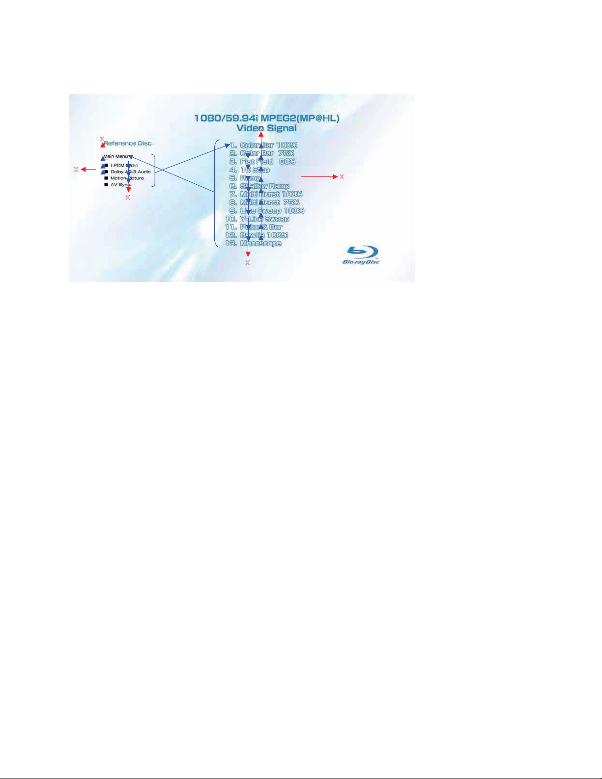
1-3-1-4. BLX-104 Menu Function (4)
Sub menu1
X
BDP-BX37/S270/S370/S373/S470
X
X
X
X
X
1) At the display of Sub menu1, 1. Color Bar 100% is selectively displayed.
t
2) Selection of 1. Color Bar 100%
Return to Sub menu1 after seamless playback from T1_C1 to T1_C13. 1. Color Bar 100% is selec-
tively displayed on Sub menu1 screen.
3) Selection of 2. Color Bar 75%
t
Return to Sub menu1 after seamless playback from T1_C2 to T1_C13. 1. Color Bar 100% is selectively
displayed on Sub menu1 screen.
4) At the selection of 3 - 13, item 3 mentioned above is executed as the routine.
t
5) At the display of Sub menu1, Main Menu is selected
Jump to Main Menu. At the display of Ma in Menu, 1. V ideo Signal of 59.94Hz/1080i
is selectively displayed.
6) Selection of LPCM Audio
t
Playback from T2_C1 to T19_C1. SubPic that corresponds to Audio stream 1 is forcibly displayed.
During the playback, when audio channel changes, the caption that corresponds to each audio stream is forcibly displayed. Return to
Sub menu1 after playback. 1. Color Bar 100% is selectively displayed on Sub menu1 screen.
t
7) Selection of Dolby AC-3 Audio
Playback of T20_C1. SubPic that corresponds to Audio stream 1 is forcibly displayed.
During the playback, when audio channel changes, the caption that corresponds to each audio stream is forcibly displayed. Return to
Sub menu1 after playback. 1. Color Bar 100% is selectively displayed on Sub menu1 screen.
8) Selection of Motion Picture
t
Return to Sub menu1 after playback of T21_C1. 1. ColorBar 100% is selectively displayed on Sub
menu1 screen.
9) At the selection of Main Menu, 1. VideoSignal of 1080/59.94i of Main Menu is selectively displayed.
10) AV Sync does not operate.
1-5
Page 9

1-3-1-5. BLX-104 Menu Function (5)
Sub menu2
X
BDP-BX37/S270/S370/S373/S470
X
X
X
X
X
1) At the display of Sub menu2, 1. Color Bar 100% is selectively displayed.
2) Selection of 1. Color Bar 100%
t
Return to Sub menu2 after seamless playback from T43_C1 to T43_C13. 1. Color Bar 100% is
selectively displayed on Sub menu2 screen.
3) Selection of 2. Color Bar 75%
t
Return to Sub menu2 after seamless playback from T43_C2 to T43_C13. 1. Color Bar 100% is se-
lectively displayed on Sub menu2 screen.
4) At the selection of 3 - 13, item 3 mentioned above is executed as the routine.
t
5) At the display of Sub menu2, Main Menu is selected
Jump to Main Menu. At the display of Main Menu, 1. Video Signal of
23.976Hz/1080P is selectively displayed.
6) Selection of LPCM Audio
t
Playback from T44_C1 to T50_C1. SubPic that corresponds to Audio stream 1 is forcibly displayed.
During the playback, when audio channel changes, the caption that corresponds to each audio stream is forcibly displayed. Return to
Sub menu2 after playback. 1. Color Bar 100% is selectively displayed on Sub menu2 screen.
t
7) Selection of Dolby AC-3 Audio
Playback of T51_C1. SubPic that corresponds to Audio stream 1 is forcibly displayed.
During the playback, when audio channel changes, the caption that corresponds to each audio stream is forcibly displayed. Return to
Sub menu2 after playback. 1. Color Bar 100% is selectively displayed on Sub menu2 screen.
8) Selection of Motion Picture
t
Return to Sub menu2 after playback of T52_C1. 1. Color Bar 100% is selectively displayed on Sub
menu2 screen.
9) At the selection of Main Menu, 1. Video Signal of 1080/23.976P of Main Menu is selectively displayed.
10)
AV Sync does not operate.
1-6
Page 10
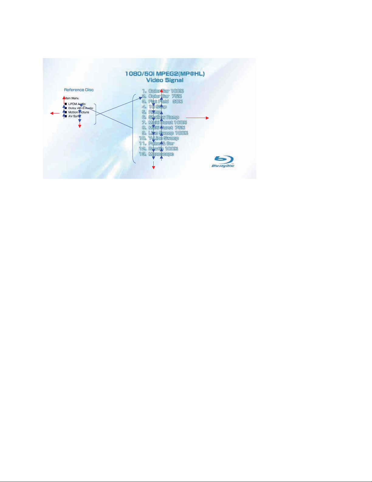
1-3-1-6. BLX-104 Menu Function (6)
Sub menu3
X
BDP-BX37/S270/S370/S373/S470
X
X
X
X
X
1) At the display of Sub menu3, 1. Color Bar 100% is selectively displayed.
2) Selection of 1. Color Bar 100%
t
Return to Sub menu3 after seamless playback from T53_C1 to T53_C13. 1. Color Bar 100% is
selectively displayed on Sub menu3 screen.
3) Selection of 2. Color Bar 75%
t
Return to Sub menu3 after seamless playback from T53_C2 to T53_C13. 1. Color Bar 100% is se-
lectively displayed on Sub menu3 screen.
4) At the selection of 3 - 13, item 3 mentioned above is executed as the routine.
t
5) At the display of Sub menu3, Main Menu is selected
Jump to Main Menu. At the display of Main Menu, 1. V ideo Signal of 50Hz/1080i
is selectively displayed.
6) Selection of LPCM Audio
t
Playback from T54_C1 to T60_C1. SubPic that corresponds to Audio stream 1 is forcibly displayed.
During the playback, when audio channel changes, the caption that corresponds to each audio stream is forcibly displayed. Return to
Sub menu3 after playback. 1. Color Bar 100% is selectively displayed on Sub menu3 screen.
t
7) Selection of Dolby AC-3 Audio
Playback of T61_C1. SubPic that corresponds to Audio stream 1 is forcibly displayed.
During the playback, when audio channel changes, the caption that corresponds to each audio stream is forcibly displayed. Return to
Sub menu3 after playback. 1. Color Bar 100% is selectively displayed on Sub menu3 screen.
8) Selection of Motion Picture
t
Return to Sub menu3 after playback of T62_C1. 1. Color Bar 100% is selectively displayed on Sub
menu3 screen.
9) At the selection of Main Menu, 1. Video Signal of 1080/50i of Main Menu is selectively displayed.
10)
AV Sync does not operate.
1-7
Page 11
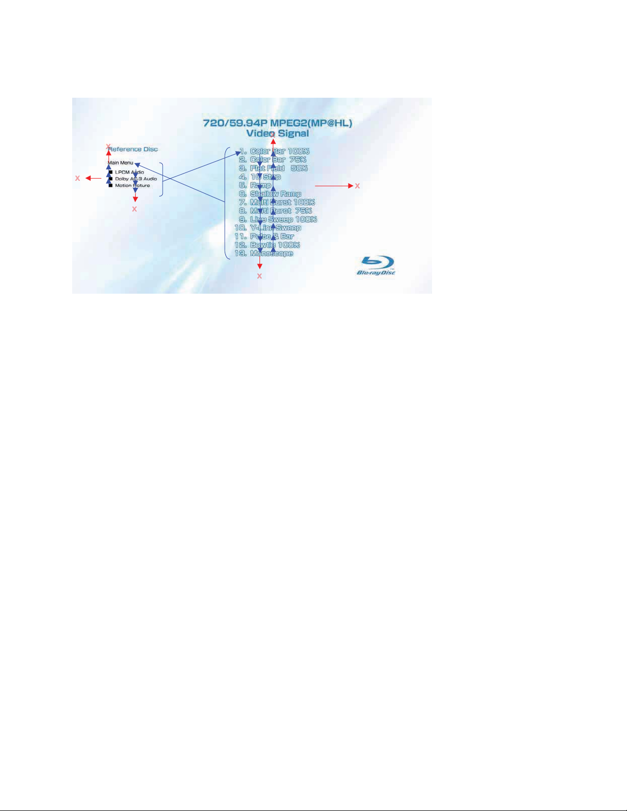
1-3-1-7. BLX-104 Menu Function (7)
Sub menu4
X
BDP-BX37/S270/S370/S373/S470
X
X
X
X
X
1) At the display of Sub menu4, 1. Color Bar 100% is selectively displayed.
t
2) Selection of 1. Color Bar 100%
Return to Sub menu4 after seamless playback from T22_C1 to T22_C13. 1. Color Bar 100% is
selectively displayed on Sub menu4 screen.
3) Selection of 2. Color Bar 75%
t
Return to Sub menu4 after seamless playback from T22_C2 to T22_C13. 1. Color Bar 100% is se-
lectively displayed on Sub menu4 screen.
4) At the selection of 3 - 13, item 3 mentioned above is executed as the routine.
t
5) At the display of Sub menu4, Main Menu is selected
Jump to Main Menu. At the display of Main Menu, 1. Video Signal of 59.94Hz/720P
is selectively displayed.
6) Selection of LPCM Audio
t
Playback from T44_C1 to T50_C1. SubPic that corresponds to Audio stream 1 is forcibly displayed.
During the playback, when audio channel changes, the caption that corresponds to each audio stream is forcibly displayed. Return to
Sub menu4 after playback. 1. Color Bar 100% is selectively displayed on Sub menu4 screen.
t
7) Selection of Dolby AC-3 Audio
Playback of T51_C1. SubPic that corresponds to Audio stream 1 is forcibly displayed.
During the playback, when audio channel changes, the caption that corresponds to each audio stream is forcibly displayed. Return to
Sub menu4 after playback. 1. Color Bar 100% is selectively displayed on Sub menu4 screen.
8) Selection of Motion Picture
t
Return to Sub menu4 after playback of T52_C1. 1. Color Bar 100% is selectively displayed on Sub
menu4 screen.
9) At the selection of Main Menu, 1. Video Signal of 720/59.94P of Main Menu is selectively displayed.
10) AV Sync does not operate.
1-8
Page 12

BDP-BX37/S270/S370/S373/S470
1-3-2
Menu Function
1-3-2-1. BLX-204 Menu Function (1)
Main Menu
X X X X
X
X
X
X
X
X
X
X
X
X
X
X
X
X
1) When the disc is inserted, 1. Video Signal of 59.94Hz/1080i of the Main Menu is selectively displayed.
1-3-2-2. BLX-204 Menu Function (2)
Main Menu
To Main Menu after playback of T83_C1
To Main Menu after playback of T62tT82
To Main Menu after playback of T61_C1
To Main Menu after playback of T54_C1-T60_C1tT83_C1-T94_C1
Sub_menu3 is displayed
To Main Menu after playback of T67_C1
To Main Menu after playback of T21tT63tT64tT65tT66
To Main Menu after playback of T20_C1
To Main Menu after playback from T2_C1 to T19_C1
Sub_menu1 is displayed
* When returning to Main Menu after playback from each button of 59.94Hz/1080i, 1. Video Signal of 59.94Hz/1080i is selectively dis-
played.
* When returning to Main Menu after playback from each button of 50Hz/1080i, 1. Video Signal of 50Hz/1080i is selectively displayed.
Note:
Txx_ Cxx
Chapter No.
Title No.
1-9
Page 13
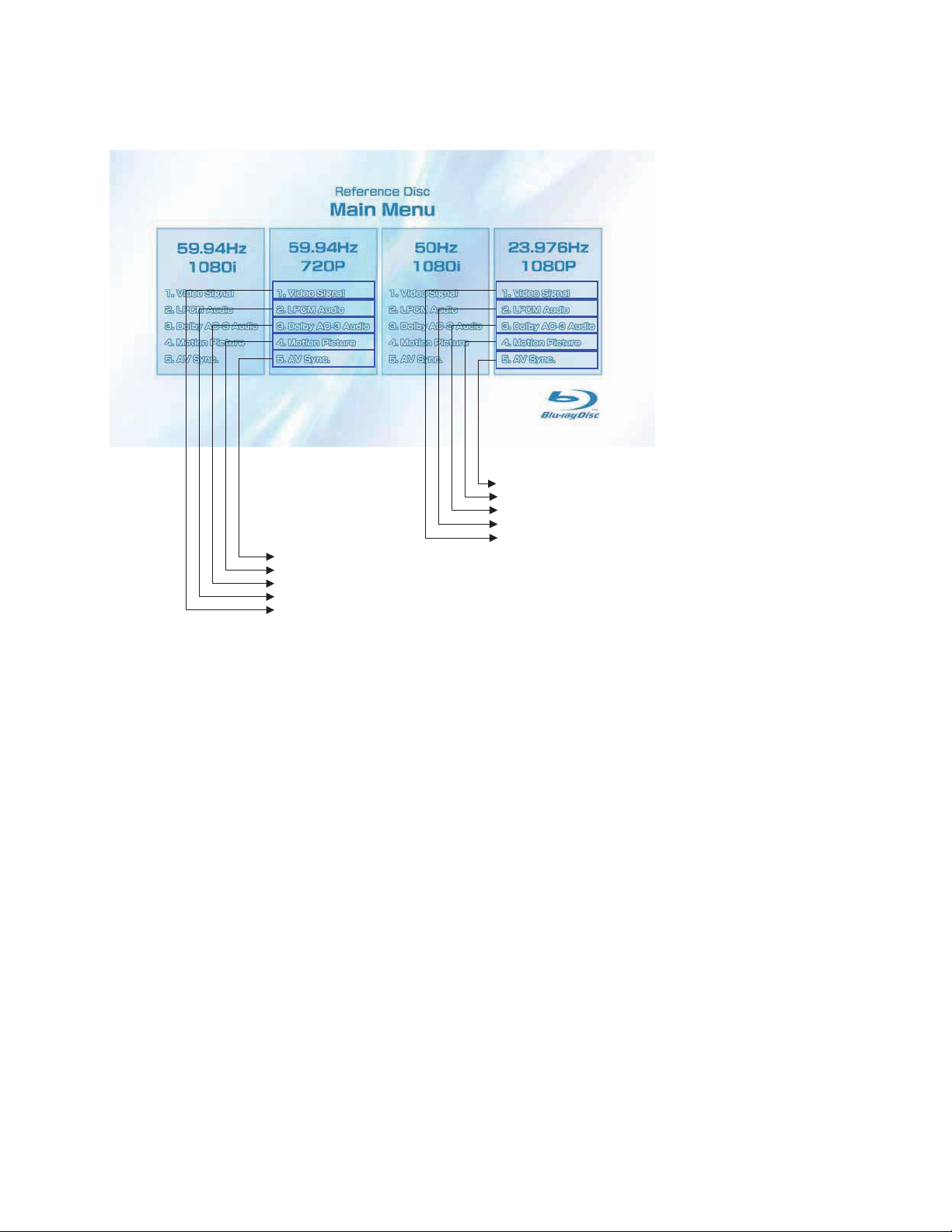
BDP-BX37/S270/S370/S373/S470
1-3-2-3. BLX-204 Menu Function (3)
Main Menu
To Main Menu after playback of T70_C1
To Main Menu after playback of T52_C1t T69
To Main Menu after playback of T51_C1
To Main Menu after playback of T44_C1-T50_C1t T71_C1-T81_C1
Sub_menu2 is displayed
To Main Menu after playback of T68_C1
To Main Menu after playback of T42_C1
To Main Menu after playback of T41_C1
To Main Menu after playback from T23_C1 to T40_C1
Sub_menu4 is displayed
* When returning to Main Menu after playback from each button of 59.94Hz/720P, 1. Video Signal of 59.94Hz/720P is selectively dis-
played.
* When returning to Main Menu after playback from each button of 23.976Hz/1080P, 1. Video Signal of 23.976Hz/1080P is selectively
displayed.
1-10
Page 14
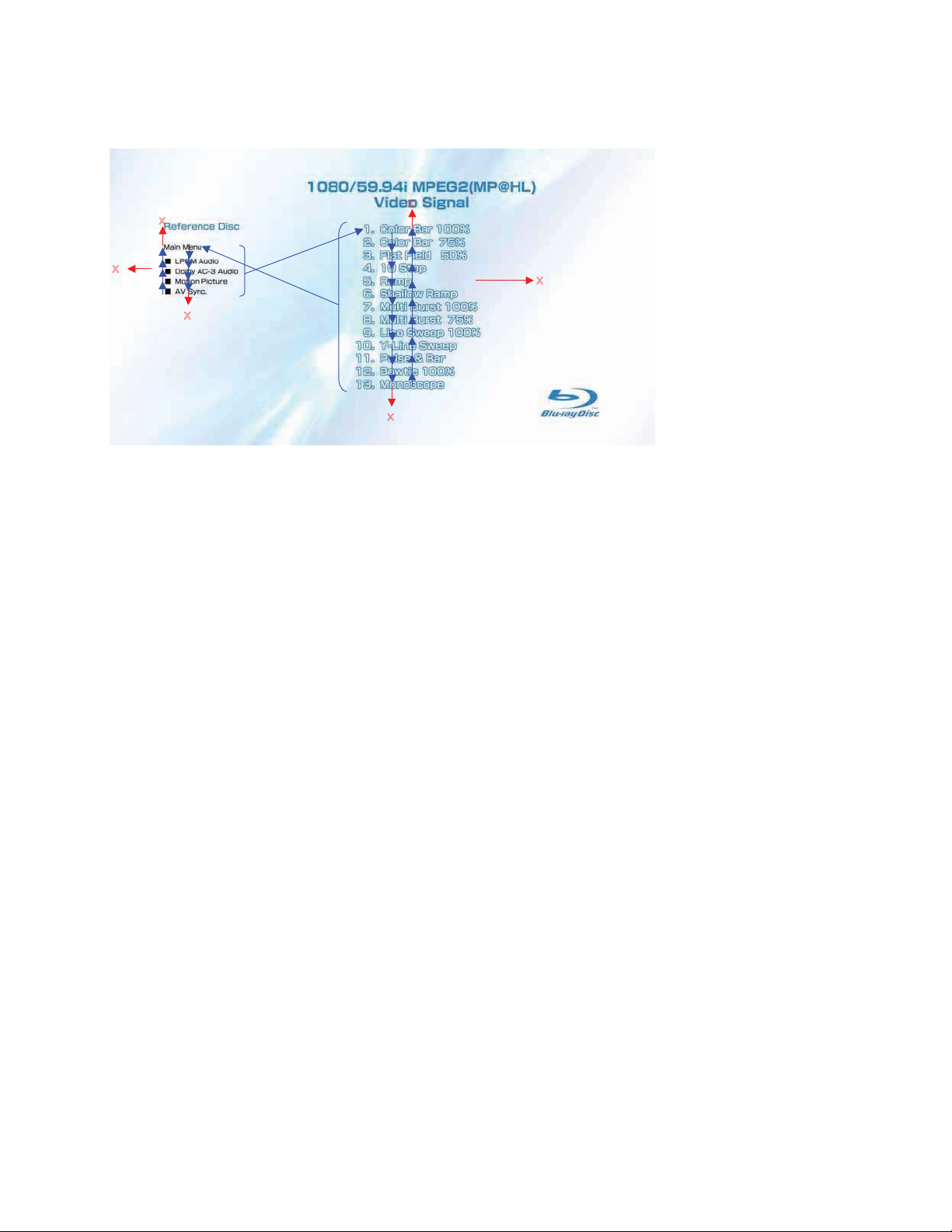
1-3-2-4. BLX-204 Menu Function (4)
Sub menu 1
X
BDP-BX37/S270/S370/S373/S470
X
X
X
X
X
1) At the display of Sub menu1, 1. Color Bar 100% is selectively displayed.
t
2) Selection of 1. Color Bar 100%
Return to Sub menu1 after seamless playback from T1_C1 to T1_C13. 1. Color Bar 100% is selec-
tively displayed on Sub menu1 screen.
3) Selection of 2. Color Bar 75%
t
Return to Sub menu1 after seamless playback from T1_C2 to T1_C13. 1. Color Bar 100% is selectively
displayed on Sub menu1 screen.
4) At the selection of 3 - 13, item 3 mentioned above is executed as the routine.
t
5) At the display of Sub menu1, Main Menu is selected
Jump to Main Menu. At the display of Main Menu, 1. Video Signal of
59.94Hz/1080i is selectively displayed.
t
6) Selection of LPCM Audio
Playback from T2_C1 to T19_C1. SubPic that corresponds to Audio stream 1 is forcibly displayed.
During the playback, when audio channel changes, the caption that corresponds to each audio stream is forcibly displayed. Return to
Sub menu1 after playback. 1. Color Bar 100% is selectively displayed on Sub menu1 screen.
7) Selection of Dolby AC-3 Audio
t
Playback of T20_C1. SubPic that corresponds to Audio stream 1 is forcibly displayed.
During the playback, when audio channel changes, the caption that corresponds to each audio stream is forcibly displayed. Return to
Sub menu1 after playback. 1. Color Bar 100% is selectively displayed on Sub menu1 screen.
t
8) Selection of Motion Picture
Return to Sub menu1 after playback of T21_C1. 1. Color Bar 100% is selectively displayed on Sub
menu1 screen.
9) Selection of AV Sync
t
Return to Sub menu1 after playback of T67_C1. 1. Color Bar 100% is selectively displayed on Sub menu1
screen.
10) At the selection of Main Menu, 1. Video Signal of 1080/59.94i of Main Menu is selectively displayed.
1-11
Page 15
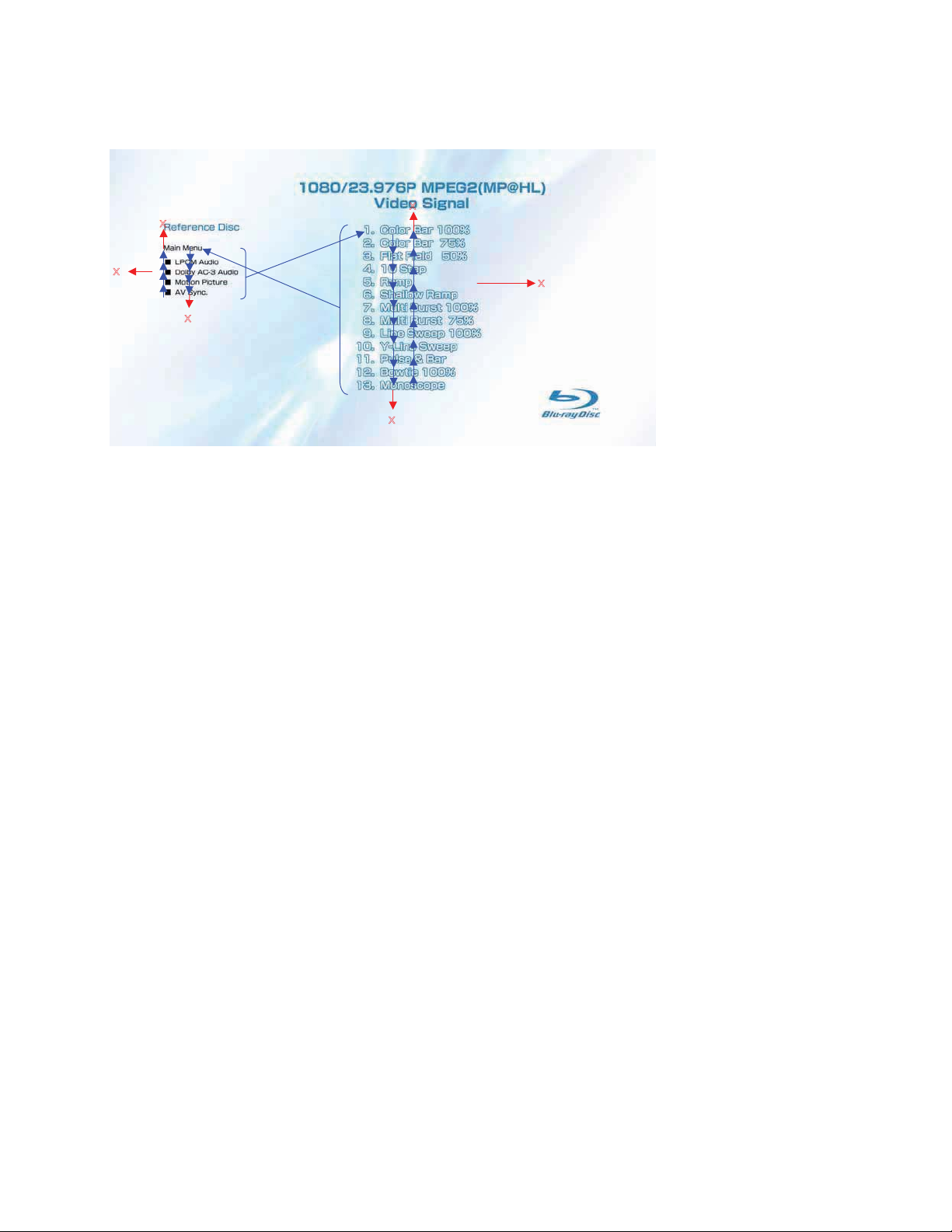
1-3-2-5. BLX-204 Menu Function (5)
Sub menu 2
X
BDP-BX37/S270/S370/S373/S470
X
X
X
X
X
1) At the display of Sub menu2, 1. Color Bar 100% is selectively displayed.
t
2) Selection of 1. Color Bar 100%
Return to Sub menu2 after seamless playback from T43_C1 to T43_C13. 1. Color Bar 100% is
selectively displayed on Sub menu2 screen.
3) Selection of 2. Color Bar 75%
t
Return to Sub menu2 after seamless playback from T43_C2 to T43_C13. 1. Color Bar 100% is se-
lectively displayed on Sub menu2 screen.
4) At the selection of 3 - 13, item 3 mentioned above is executed as the routine.
t
5) At the display of Sub menu2, Main Menu is selected
Jump to Main Menu. At the display of Main Menu, 1. Video Signal of
23.976Hz/1080P is selectively displayed.
6) Selection of LPCM Audio
t
Playback from T44_C1 to T50_C1 and from T71_C1 to T81_C1. SubPic that corresponds to Audio stream
1 is forcibly displayed.
During the playback, when audio channel changes, the caption that corresponds to each audio stream is forcibly displayed. Return to
Sub menu2 after playback. 1. Color Bar 100% is selectively displayed on Sub menu2 screen.
t
7) Selection of Dolby AC-3 Audio
Playback of T51_C1. SubPic that corresponds to Audio stream 1 is forcibly displayed.
During the playback, when audio channel changes, the caption that corresponds to each audio stream is forcibly displayed. Return to
Sub menu2 after playback. 1. Color Bar 100% is selectively displayed on Sub menu2 screen.
t
8) Selection of Motion Picture
Return to Sub menu2 after playback of T52_C1 and T69. 1. Color Bar 100% is selectively displayed on
Sub menu2 screen.
9) Selection of AV Sync
t
Return to Sub menu2 after playback of T70_C1. 1. Color Bar 100% is selectively displayed on Sub menu2
screen.
10) At the selection of Main Menu, 1. Video Signal of 1080/23.976P of Main Menu is selectively displayed.
1-12
Page 16
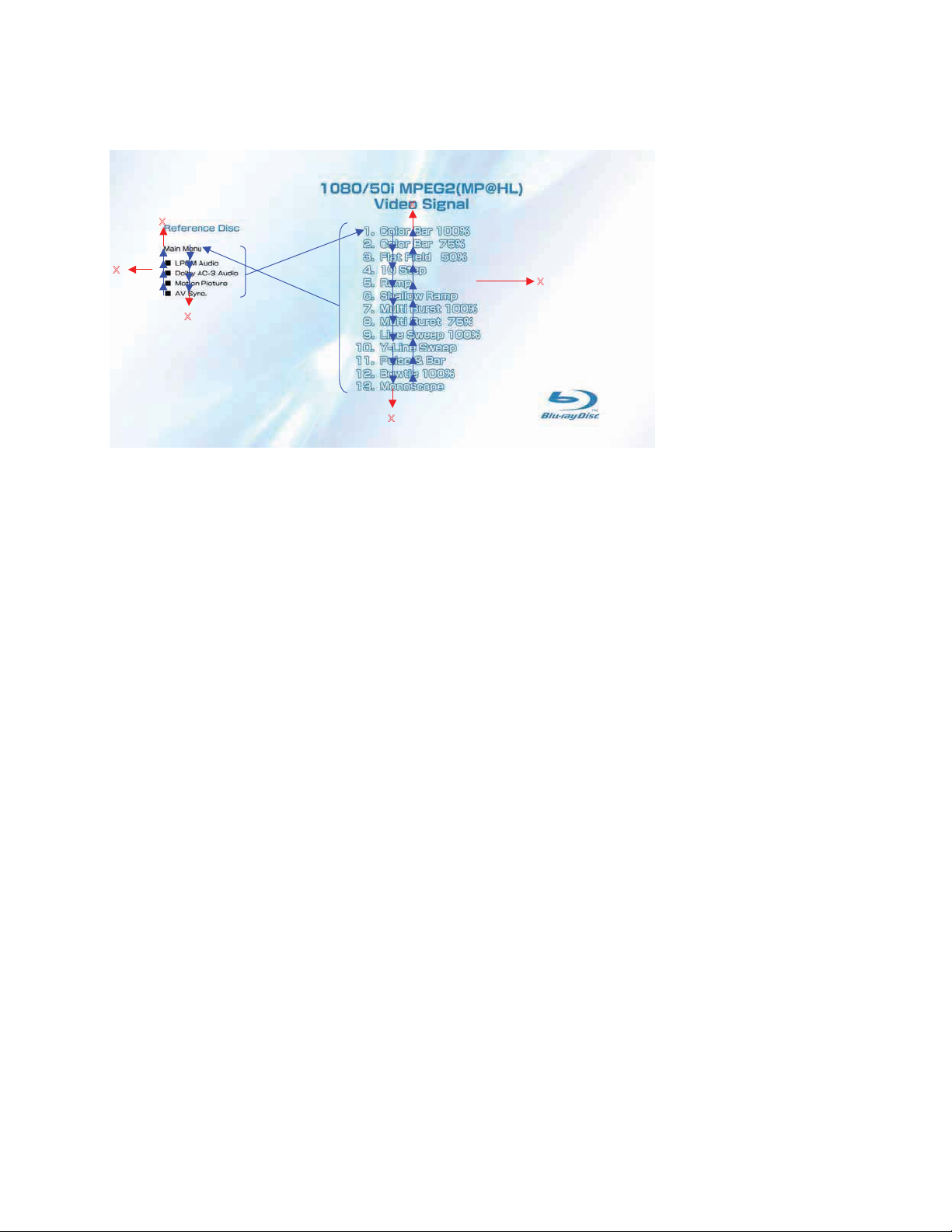
1-3-2-6. BLX-204 Menu Function (6)
Sub menu 3
X
BDP-BX37/S270/S370/S373/S470
X
X
X
X
X
1) At the display of Sub menu3, 1. Color Bar 100% is selectively displayed.
t
2) Selection of 1. Color Bar 100%
Return to Sub menu3 after seamless playback from T53_C1 to T53_C13. 1. Color Bar 100% is
selectively displayed on Sub menu3 screen.
3) Selection of 2. Color Bar 75%
t
Return to Sub menu3 after seamless playback from T53_C2 to T53_C13. 1. Color Bar 100% is se-
lectively displayed on Sub menu3 screen.
4) At the selection of 3 - 13, item 3 mentioned above is executed as the routine.
5) At the display of Sub menu3, Main Menu is selected
t
Jump to Main Menu. At the display of Main Menu, 1. V ideo Signal of 50Hz/1080i
is selectively displayed.
t
6) Selection of LPCM Audio
Playback from T54_C1 to T60_C1 and from T84_C1 to T94_C1. SubPic that corresponds to Audio stream
1 is forcibly displayed.
During the playback, when audio channel changes, the caption that corresponds to each audio stream is forcibly displayed. Return to
Sub menu3 after playback. 1. Color Bar 100% is selectively displayed on Sub menu3 screen.
t
7) Selection of Dolby AC-3 Audio
Playback of T61_C1. SubPic that corresponds to Audio stream 1 is forcibly displayed.
During the playback, when audio channel changes, the caption that corresponds to each audio stream is forcibly displayed. Return to
Sub menu3 after playback. 1. Color Bar 100% is selectively displayed on Sub menu3 screen.
8) Selection of Motion Picture
t
Return to Sub menu3 after playback of T62_C1 and T82. 1. Color Bar 100% is selectively displayed on
Sub menu3 screen.
t
9) Selection of AV Sync
Return to Sub menu3 after playback of T83_C1. 1. Color Bar 100% is selectively displayed on Sub menu3
screen.
10) At the selection of Main Menu, 1. Video Signal of 1080/50i of Main Menu is selectively displayed.
1-13
Page 17
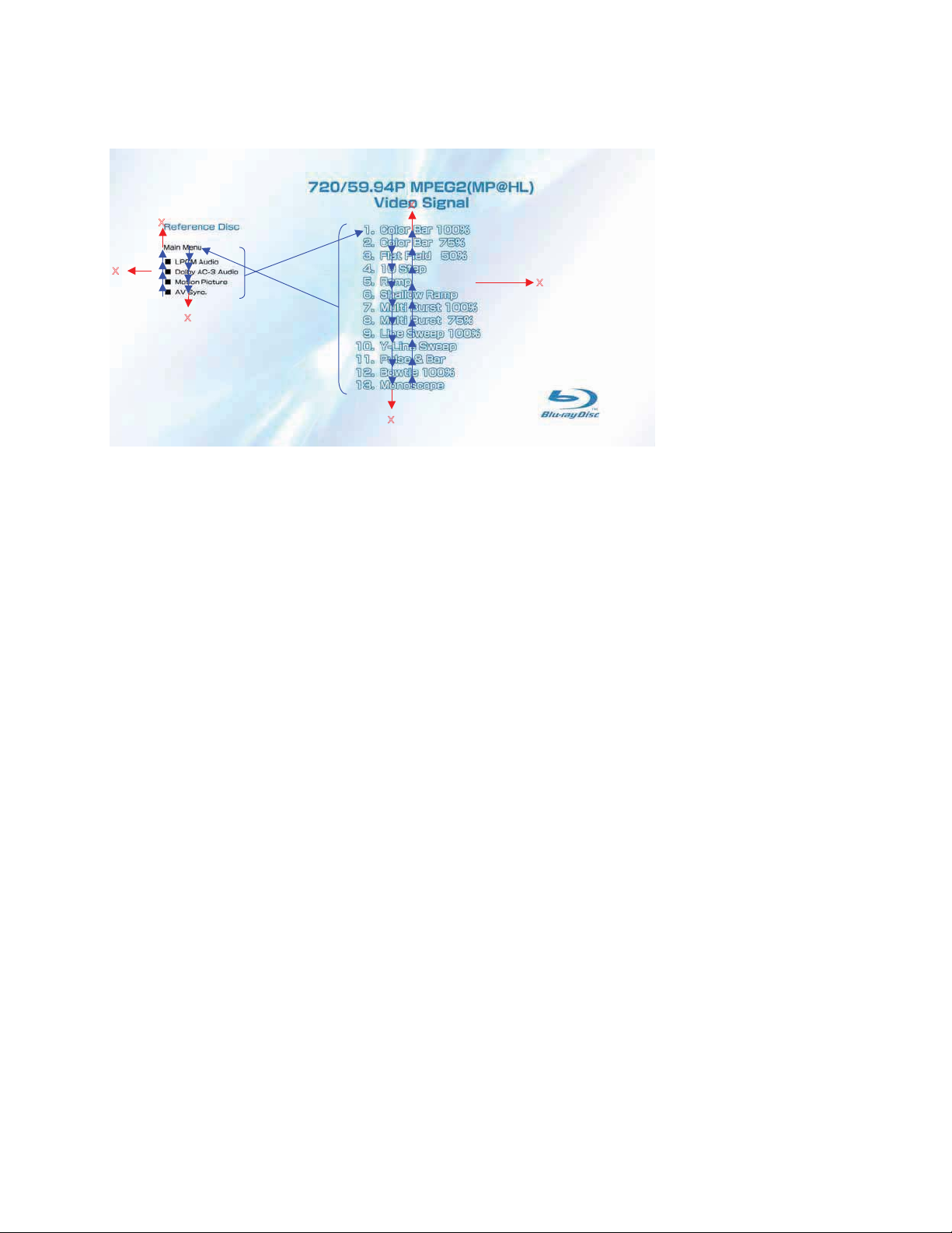
1-3-2-7. BLX-204 Menu Function (7)
Sub menu 4
X
BDP-BX37/S270/S370/S373/S470
X
X
X
X
X
1) At the display of Sub menu4, 1. Color Bar 100% is selectively displayed.
t
2) Selection of 1. Color Bar 100%
Return to Sub menu4 after seamless playback from T22_C1 to T22_C13. 1. Color Bar 100% is
selectively displayed on Sub menu4 screen.
3) Selection of 2. Color Bar 75%
t
Return to Sub menu4 after seamless playback from T22_C2 to T22_C13. 1. Color Bar 100% is se-
lectively displayed on Sub menu4 screen.
4) At the selection of 3 - 13, item 3 mentioned above is executed as the routine.
t
5) At the display of Sub menu4, Main Menu is selected
Jump to Main Menu. At the display of Main Menu, 1. Video Signal of 59.94Hz/720P
is selectively displayed.
6) Selection of LPCM Audio
t
Playback from T44_C1 to T50_C1. SubPic that corresponds to Audio stream 1 is forcibly displayed.
During the playback, when audio channel changes, the caption that corresponds to each audio stream is forcibly displayed. Return to
Sub menu4 after playback. 1. Color Bar 100% is selectively displayed on Sub menu4 screen.
t
7) Selection of Dolby AC-3 Audio
Playback of T51_C1. SubPic that corresponds to Audio stream 1 is forcibly displayed.
During the playback, when audio channel changes, the caption that corresponds to each audio stream is forcibly displayed. Return to
Sub menu4 after playback. 1. Color Bar 100% is selectively displayed on Sub menu4 screen.
8) Selection of Motion Picture
t
Return to Sub menu4 after playback of T52_C1. 1. Color Bar 100% is selectively displayed on Sub
menu4 screen.
t
9) Selection of AV Sync
Return to Sub menu4 after playback of T68_C1. 1. Color Bar 100% is selectively displayed on Sub menu4
screen.
10) At the selection of Main Menu, 1. Video Signal of 720/59.94P of Main Menu is selectively displayed.
1-14
Page 18
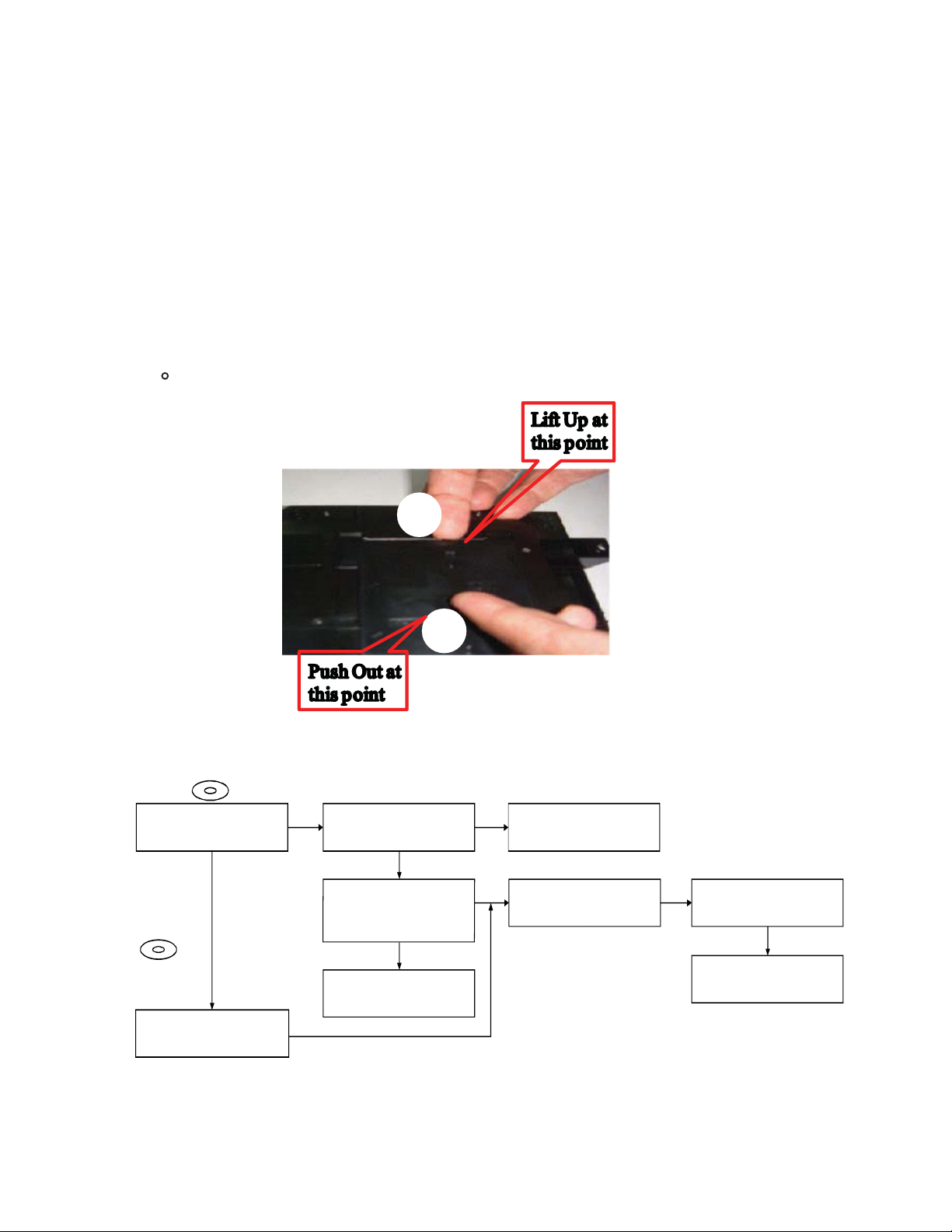
1-4.
DRIVE REPAIRING
1-4-1. Preparation
• ESD Measures
It is necessary to check the working space ESD condition
before starting the Drive Part (BU) repairs
The ESD-resistance of BD Laser is weaker than DVD/CD Laser
To prevent ESD destruction, please make sure the working
space and human ESD.
How to open FFC Holder. Refer below picture.
•
BDP-BX37/S270/S370/S373/S470
1-4-2.
Checking Flow ~ Drive (BU) section ~
Dri ve f lo wc har t
BLX-104
BDP-S370 can play the BD-disc
YES
DVD: HLX-513
CD: HLX-A1
NO
Check / replace the FFC cable, then check
1
1
2
2
1
2
Check Drive Power Supply
CN301 Pin 2: 12V / Pin 6: 5V
YES
BDP-S370 operates normally
OP FFC cable (1-837-494-11)
SPDL FFC cable (1-837-495-11)
YES
OK
NO
Check PS301, PS302, PS303
Replace PS when open
Check the Optical Block Unit (BU) by
NO
service mode. (Flowchart zz)
BU IOP is OK?
NO
Replace the Optical Block Unit (BU)
Optical Block Unit (BU) replace
(Flowchart yy)
BDP-S370 can play the DVD/CD-disc
NO
1-15
Page 19

1-4-3. BU Check Flow [zz] ~
BDP-BX37/S270/S370/S373/S470
Before
Optical Block Unit (BU) IOP check flow (zz) ~ [Before BU Replacement]
Enter Service Mode
<OPEN/CLOSE>., <PLAY>,<STOP>
Press
and plug in AC Power
Inside *Service Mode Menu
Select [8] Drive
Inside *Drive
Select [7] OP Check Menu
Inside *OP Check Menu
Select [3] dIOP then press 'ENTER'
Specification dIOP
BD: 6mA
DVD, CD: 9mA
AC Power OFF
1-4-4. BU (Optical Block) Repair Guide
+
+
-
YES
BU Replacement ~
NO
IOP out of specification need BU
replacement
Optical Block Unit (BU) replace
(Flowchart yy)
BDP 5G (BDP-S370) series component structure is as same as conventional DVD Players.
However BD player requires precise read out functions and also secure contents Protection
system.
Since above requirement, it is necessary to set/adjust BU data to EEPROM.
The following cases need Adjustments;
(1)Replace BU (MB is original)
(2)Replace MB (BU is original)
(3)Replace both BU and MB
•JIG Requirement
Digital camera (recommend with macro mode)
Barcode decoder (5GBUJIG) installed in JIG PC’s
USB memory
ESD work bench
•Procedure (all cases)
Refer the diagram
Remarks:
The servo adjustment procedure will be carried out during OP data Writing.
There is no manual adjustment procedure. LD ON TIME history doesn’t carry over.
Do not touch any optical block parts, Turn Table and during replacing. BD Laser diode
is very sensitive!
1-16
Page 20
O ptic al Bloc k Unit ( BU) OP Da ta Write Flow (y y ) ~ [After BU/MB R epla c ement]
Remove the defective BU from Loading
Assy and also remove BU insulator (4pcs)
Unpack new BU and take OP Data Barcode
Assemble BU with Insulators to Loading
Decode the OP Data Barcode phot using
BDBUDEC.exe
Enter Service Mode and insert USB memory
And confirm dIOP by select [7] OP Check
IOP in specification --> Turn AC Power OFF
photo by camera
Assy (tighten screw with 2kgf)
USB memo r y(File Name: BuData.txt)
Select [1] Drive OP data Write -->
After Finishing ReWrite OP data
Menu to verify IOP in specification
and save the test data to
to USB connector
Select [8] Drive -->
Select [2] Mode: 1 or 2
Press ENTER
--> Turn AC Power OFF
The following cases need O P D ata Write:
(1) Replace BU (MB is original)
(2) Replac e MB (BU is original)
(3) Replace both BU and MB
JIG requirement
Digital camera (with macro mode)
Barcode decoder (BDBUDec.exe )
installed in jig
PC's (jig purpose)
USB memory
ESD free work bench
Explanation:
Mode: 1 -->
Mode: 2 -->
BDP-BX37/S270/S370/S373/S470
BDP-BX57/S570
Turn Power ON and check playback
performance using BD, DVD and CD
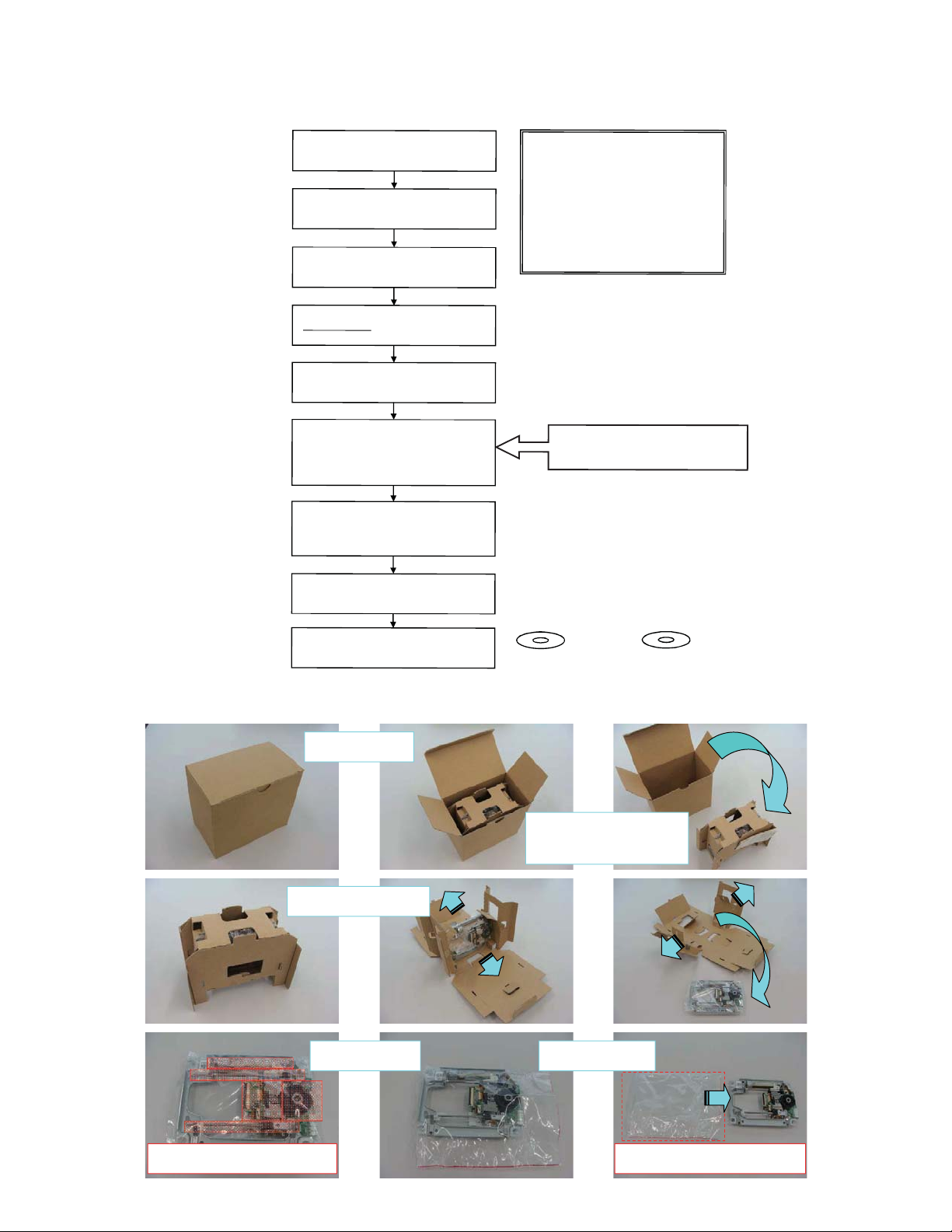
KEM-430AAA/C2RP Packing Spec.
BLX-104
DVD: HLX-513
CD: HLX-A1
Open a box
Take a corrugated
cushion out
Open a cushion
Open a bag
Take BU out
Don’t touch the area!!
Don’t Reuse the bag!!
Page 21

1-4-7. KEM-460AAA/C2RP Packing
BDP-BX37/S270/S370/S373/S470
1) Store it in Cushion Carton
Antistatic Bag
Cushion Carton (E430-BU-RP)
2) Store it in Individual Carton
Instruction
Manual
1 Process the bend of FFC.
(Do as well as the state when mass
production is packed)
2 It is necessary to fold the antistatic
bag in order of A to B .
(Purpose: Toapply loosening to part C )
3 Set the upper s
the part of the 14 hole.
urface of the turntable to
Thing that is stopper of OP.
The side with the turned flap is a
lid side of the individual carton.
Individual Carton (E430-BU-RP)
3) Store it in Master Carton
Store 10 individual cartons 1 step X 2 steps
= 20 individual cartons in the master carton.
Master Carton (E430-BU-RP)
4) Master carton is sealed
with the PP tape.
Shipment Label
(Care Mark 3)
Individual Carton (E430-BU-RP)
PP Tape
Stick it to H.
1-18
Page 22
1-6. Power Cord Soldering Location
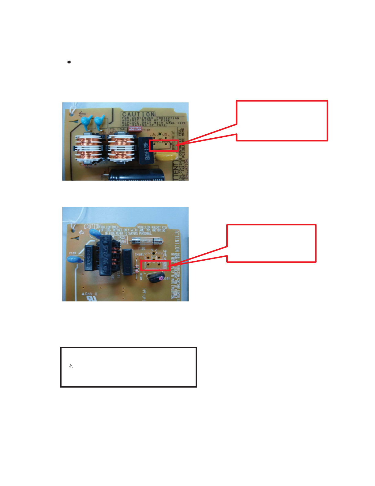
Follow the designated destination according to the mark indicated on the board
1-6-1. Soldering point for Switching Regulator (APS-257)
BDP-BX37/S270/S370/S373/S470
BDP-S270/S370/S373/S470:
EXCEPT US,CND,MX please
follow the indication marked
for soldering.
1-6-2. Soldering point for Switching Regulator (SRV2206UC)
Notes:
For BDP-S370/S470 : Taiwan ONLY
Caution :
When changing the power cord must
change the power block as well
BDP-BX37/S270/S370/S470:
US,CND,MX ONLY please
follow the indication marked
for soldering.
1-27
Page 23
BDP-BX37/S270/S370/S373/S470
1-7. Remove PT Protection on MB-134 (Service Assy Main Board)
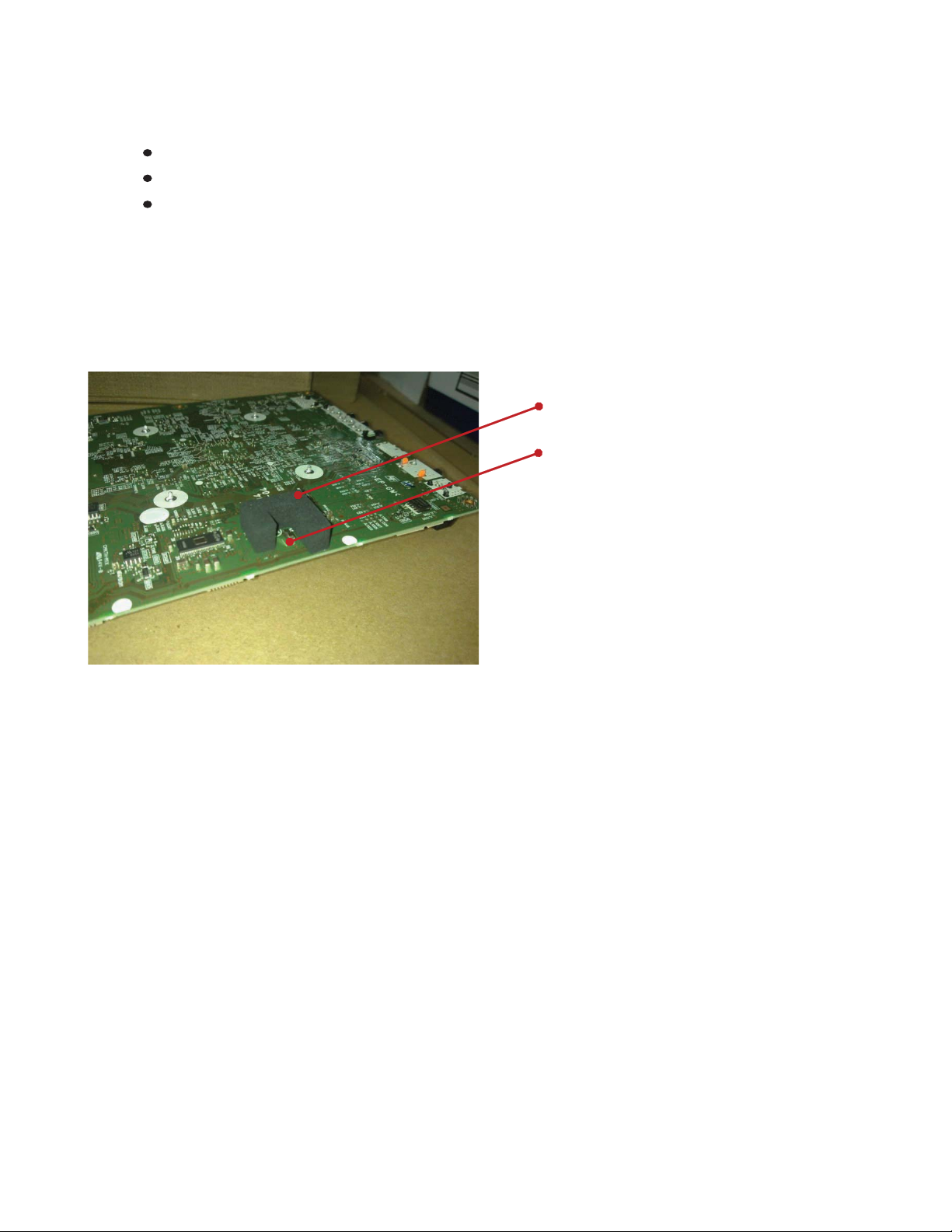
PT Protector (4-186-977-01) stick on B-side to protect PT107 (1-780-638-22)
PT Protector need to be remove before installing the MB board on chassis
Aected model :
- BDP-BX37: CND, US
- BDP-S270: BR, CND, MX, US
- BDP-S370: AR, BR, CND, E, PX, TW, US
- BDP-S470: AR, BR, CND, E, TW, US
PT Protector (P/N 4-186-977-01)
PT 107 (P/N 1-780-638-22)
1-28E
Page 24

•
This set can be disassembled in the order shown below.
2-1. DISASSEMBLY FLOW
SET
2-2. UPPER CASE
(Page 2-1)
2-3. TRAY COVER ASSY
(Page 2-2)
FRONT PANEL ASSY
2-4. BD DRIVE
(Page 2-3)
2-5.
SWP & SWB boards
(Page 2-2)
2-6. REAR PANEL
(Page 2-3)
BDP-BX37/S270/S370/S373/S470
SECTION 2
DISASSEMBLY
Note:
Follow the disassembly procedure in the numerical order given.
2-2. UPPER CASE
1 tapping screw
(tightening torque =5 to 6
kgf•cm)
2-7. MB-134 BOARD
(Page 2-4)
2
three screws
(tightening torque =
2-8. SWITCHING REGULATOR
(Page 2-4)
5 to6
kgf•cm)
tapping screw
(tightening torque = 5 to 6kgf•cm)
Upper case
3
2-1
Page 25

2-3. TRAY COVER ASSY
3 Tray cover assy
BDP-BX37/S270/S370/S373/S470
1 Insert a clip in the hole of a drive
and open a tray.
tray
2
2-4. BD DRIVE
5 BD drive
four screws (BV3)
1
(tightening torque = 6 to 7 kgf•cm)
2
Optical flexible flat cable
(CN1401)
Splindle flexible flat cable
3
(CN2460)
4
Loading flexible flat cable
(CN2470)
2-2
Page 26
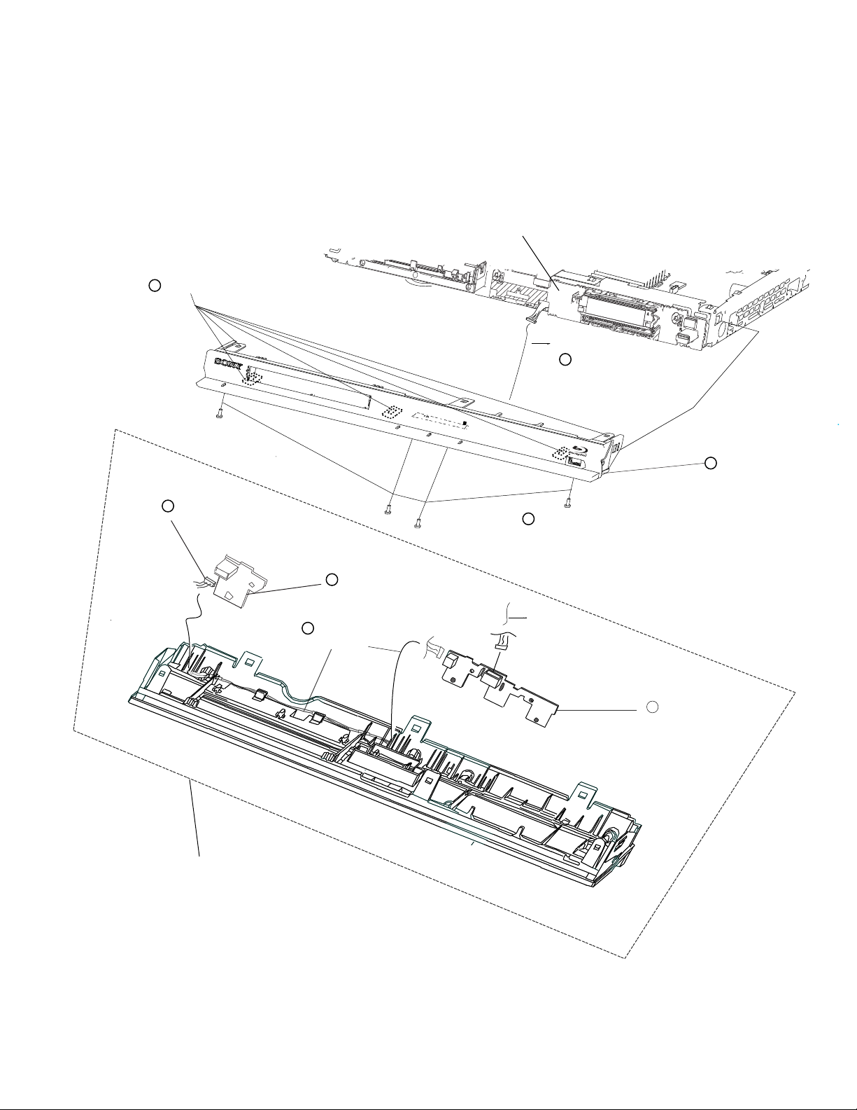
BDP-BX37/S270/S370/S373/S470
2-5. FRONT PANEL ASSY, SWB-001 AND SWP-001 BOARD
FR-309 Board
six claws
2
a
3
Harness (SIM-001)
CN402
7
Harness (BP-054)
CN331
8
SWP-001 Board
5
Harness (BP-054)
CN401
1
four screws (BV3)
(tightening torque = 2 to 3 kgf•cm)
a
6
4
Front Panel
SWB-001 Board
Front Panel inside view
2-3
Page 27
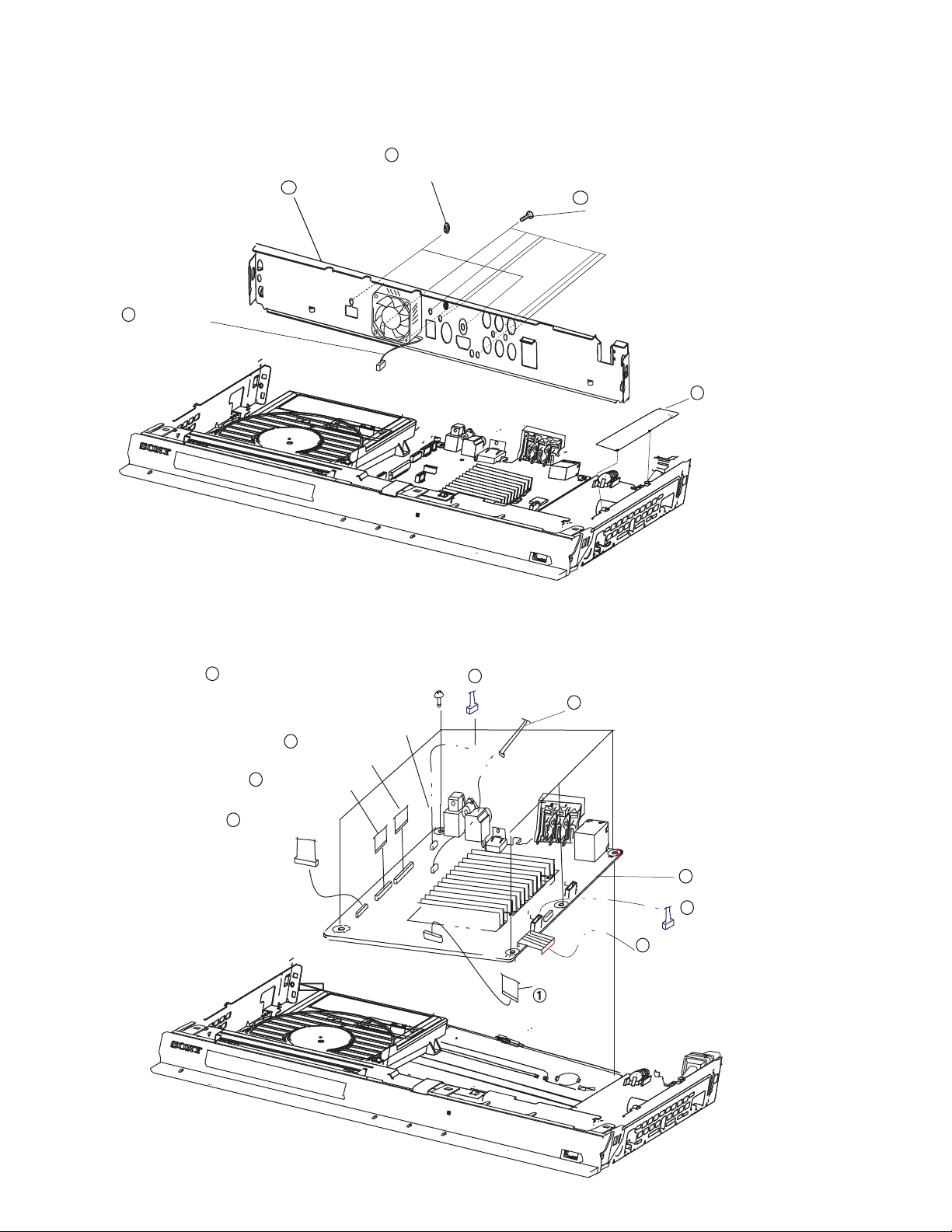
2-6. REAR PA NEL BLOCK
5
rear panel block
fan harness
1
(CN1503)
Two screws (B3)
4
(tightening torque = 4 to 5 kgf•cm)
BDP-BX37/S270/S370/S373/S470
2
‘black’ seven screws (BV3)
(tightening torque = 6 to 7 kgf•cm)
insulator PS top
3
2-7. MB-134 BOARD
Five screws (BV3)
9
(tightening torque = 6 to 7 kgf•cm)
7
8
flexible flat cable
(CN2470)
6
flexible flat cable
(CN1401)
flexible flat cable
(CN2460)
4 harness
(CN1503)
5 harness (USB-007)
(CN501)
10
2 harness (SIM-001)
Board to board
3
(CN301)
flexible flat cable (FIM-026)
(CN1504)
MB-134 board
(CN1509)
2-4
Page 28
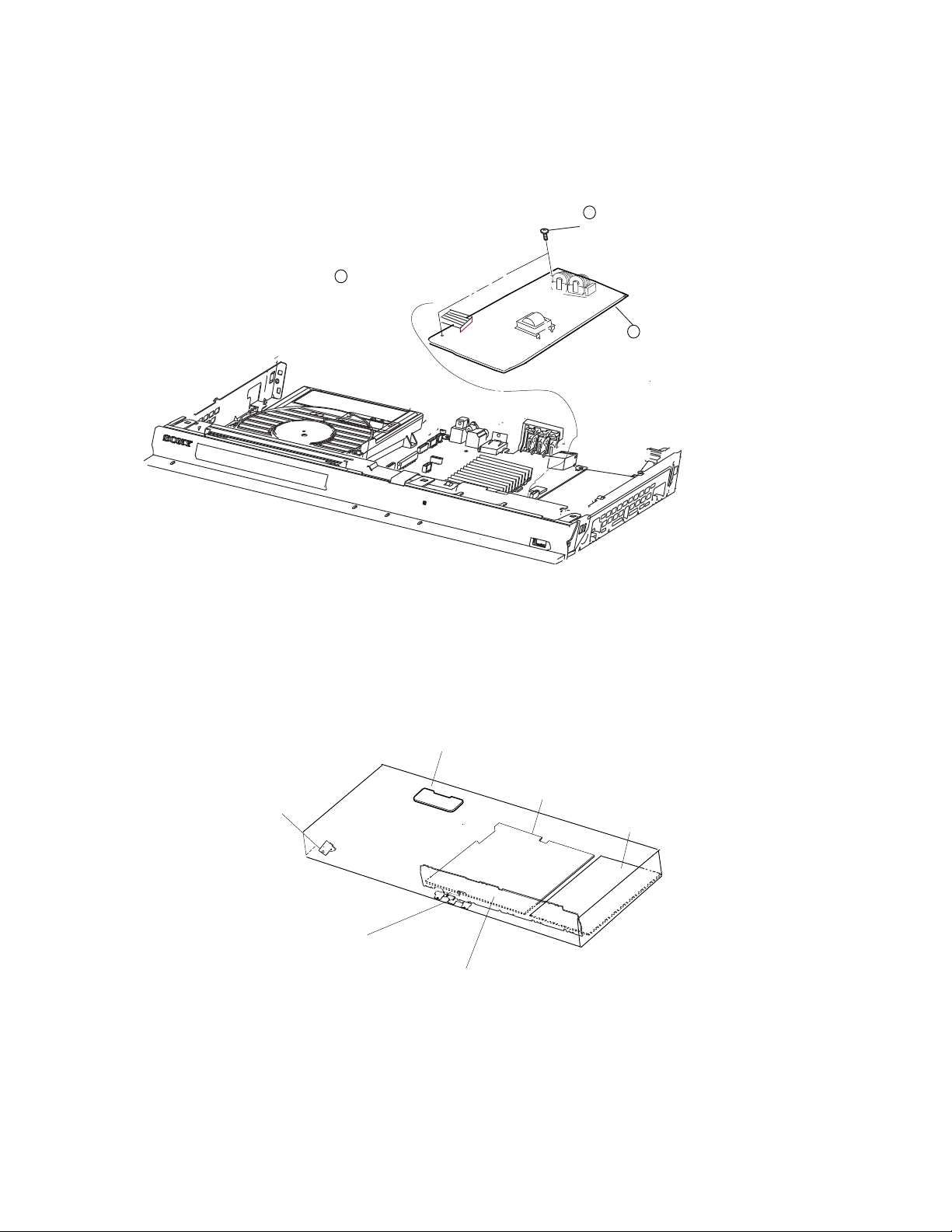
2-5
2-8. SWITCHING REGULATOR
Board to board
2-9. C IRCU IT BO ARDS LOCA TION
2
(CN301)
two screws (BV3)
1
(tightening torque = 5.5 to 7.5 kgf•cm)
3
switching regulator
SWP-001 board
USB-023 board
MB-134 board
Switching Regulator
SWB-001 board
FR-309 board
Page 29

BDP-BX37/S270/S370/S373/S470
(AC IN)
SWITCHING
REGULATOR
Y
J904
VIDEO OUT
COMPONENT
B
R
P
P
IC1003
VIDEO AMP
VIDEO
VIDEO
LINE OUT
AUDIO
J902
L
R
IC901
D/A CONVERTER
AUDIO
AUDIO
(ANALOG OUTPUT)
DIGITAL
DIGITAL OUT
PCM/DTS/DOLBY
COAXIAL
(DIGITAL OUTPUT)
CN701
OPTICAL
IC904
OPTICAL
TRANSMITTER
HDMI
IC101
USB I/F
CXD9983GG/CXD9984GG
SATA I/F, MEMORY CONTROL,
MAIN SYSTEM CONTROL, DSP
A/V OUT, HDMI, ETHERNET I/F,
HDMI OUT
USB
USB
USB-023
BOARD
REAR
USB
EXT
CN361
)
0
1
0
0
1
2
(
N
N1
A
C
L
Y
H
P
T
1
E
20
N
1
C
ER
I
H
T
E
ETHERNET
REGULATOR
Z
1
0
H
2
M
1
5
X
2
601
C
I
01
02
3
3
C
C
I
I
DDR2_1.8V
VREF_0.9V
PS301
PS302
803
703
704
C
C
C
I
I
I
03
04
05
3
3
3
C
C
C
I
I
I
CPU1.2V
DDR2_VTT0.9V
AVDD12_HDMI
CPU3.3V
AVDD33_HDMI
CORE_STB3.3V
PS303
PS304
804
C
I
07
08
3
3
C
C
I
I
FE_SW5V
FE_SW12V
DAC3.3VA
09
10
3
3
C
C
I
I
USB5V
UNSW3.3V
HDMI5V
CN1503
FAN
IC1501
The comp on en ts i den ti fi ed by
M1501
3
2
CONTROL
or d o t t ed l i ne wit h mark
are critical for safety.
mark
Replace only with part number
specifi ed.
3-1
FAN
1
X802
X401
27MHZ
SA
IC2301
DRIVE
IC2401
MOTOR
DRIVE
A-BUS
B-BUS
IC104
IC204
IC105
IC205
FRONT
IC501
FLASH
2G/16G NAND
IC502
16M
S-FLASH
25MHZ
POWER-1
UNSW6V
A
IC1504
P FAIL
IC1503
CONTROL
SUB SYSTEM
MB-134 BOARD
IC702
SECTION 3
BLOCK DIAGRAMS
Blu-ray
DVD
DRIVE
BD DRIVE
S401
S402
STOP
S403
PLAY
OPEN/CLOSE
SWB-001 BOARD
3-1. OVERALL BLOCK DIAGRAM
1 BOARD
S331
0
0
-
P
W
S
POWER
FL DRIVER
TUBE
ND701
INDICATOR
FLUORESCENT
FR-309 BOARD
PS701
FR_6V
IC701
REMOTE
CONTROL
RECEIVER
FR_6V
D702
DC/DC
Q706,Q707
CONVERTER
T701
(WHITE)
USB
EXT
CN371
EXCEPT:
BDP-S270
Page 30

BDP-BX37/S270/S370/S373/S470
MB-134 BOAR D
IC104
SDRAM
1Gb DDR2
DODQ0-DODQ15
DOA0-DOA12
FE_RFIP2
FE_RFIP
FE_RFIN
Y2
Y4
W1
BD_ RF+
BD_ RF-
DVD_RF+
DVD_RF -
22
23
26
A_RBA0
FE_RFIN2
W3
25
BA0 - BA2
L1 L-L3
AT28
A_RBA1
FE_INA
P2
A
32
/RAS
K7
L7
BB28, AU27,
BB24
AU23
A_RBA2
A_RCASB
A_RRASB
FE_INB
FE_INC
N1
R3
B
C
28
303133
A25
NS_XTALI
IC2401
V
U
44
42
V
4
3
X802
25MHZ
BA9
BB8
NXTAL25MO
MOTOR DRIVE
W
46
W
2
IC205
1Gb DDR2
DIDQ16-DIDQ31
FE_TRAYPWM
AE3
NSTAL25MI
19
VLOAD
LOAD_N
33
LOAD+
LOAD-
1
SDRAM
LOAD_ P
32
2
/RAS
BA0 - BA2
L1 L-L3
K7
FE_TRAY_OUT
FE_TRAY_IN
AJ5
AK4
CPU_NFD0 - CPU_NFD7
TRAY-IN
TRAY-OUT
3
5
IC501
/CAS
L7
/WE
ODT
K9
K3
CPU_NFCLE
CPU_NFCEN
M38
K38
9
16
cLE
nCE
2Gb/16Gb
NAND FLASH
CK
/CK
K8
J8
N41
N43
B_RCLK1
B_RCLK1B
CPU_NFALE
CPU_NFWEN
L37
G43
18
17
WE
ALE
K2
19
CKE
/CS
L8
CPU_NFREN
M36
8
nRE
CPU_NFRBN
P38
7
RY/BY
PAGE 3-4
CPU_XRST
3-2
IC105
SDRAM
CK
/CK
/CAS
/WE
ODT
CKE
/CS
L8
K2
J8
K8
K9
K3
1Gb DDR2
BA0 - BA2
L1 L-L3
CK
/CK
/CAS
/WE
ODT
/RAS
J8
K7
K8
K9
K3
L7
DODQ16-DODQ31
BA39
AV24
BA29
BA21
BC21
BC29
AW23
WEB
A_RODT
A_R
A_RCSB
A_RCLK0
A_RCLKB
A_RCLKE
BC39
A_RCLK1
A_RCLK1B
IC204
SDRAM
CKE
K2
1Gb DDR2
/CS
L8
BA0 - BA2
L1 L-L3
CK
/CK
/CAS
/WE
ODT
CKE
/RAS
K7
L7
/CS
L8
K2
J8
K8
K3
K9
DIDQ0-DIDQ15
DIA0-DIA12
93CA
,63DA ,04DA
B_RBA0
B_RBA1
B_RBA2
AJ41
B_RRASB
AH40
B_RCASB
AL43
AC41
AL41
AC43
AD42
AG41
B_RODT
B_RCSB
B_R WEB
B_RCLK0
B_RCLKE
B_RCLK0B
USB I/F,
IC101
MAIN SYSTEM CONTROL,
FE_INE
FE_INF
FE_INH
FE_IND
FE_ING
FE-OSCEN
FE_CFREQ
FE-CMOD
THER MO
U1
T6
V6
E
D
F
20
M4
R1
T2
AF8
AD2
AE7
G
H
SDIO
THER MO
SCLK
LDD_SEN
8
7
6
34
19
17
SA_B+
AF6
SA_B
STP1+
16
39
DSP,SATA I/F,MEMORY CONTROL
FE_FMO4
8
ST P1_IN
IC2301
SA_B-
SA_A
STP1-
171819
38
A/V OUT,HDMI,ETHERNET I/F
FE_GAINSW1
FE_FMO3
AE5
AG7
STEP_ENA
9
7
ST P2_IN
STEP _ENA
SA_DRIVE
STP2+
STP2-
SA_A-
SA_A+
37
36
CN1401
CXD9983GG/CXD9984GG
CPU_SFCK
CPU_SFCS
CPU_SFDO
CPU_SFDI
J39
G41
H40
F42
526
1
SI
CS
SO
SCK
IC502
16Mb
NOR -FLASH
7
PAGE 3-4
CPU_PRERST (2/2)
FD1
FCS_P
2740
X401
FE_FMO
FE_FMO2
FE_LIMIT
FE_TLO
3
G
A
AE1
AD4
AH6
AF4
AM8VTLT
FE_DMD0
AF2
27MHZ
C25
NS_XTALO
SPDL
12
17
16
VSLED1
MONITOR
SLED2_P
55
A
8
A-
9
SLED2_N
SLED1_P
56
52
B+
6
18
VSPIN
B-
SLED2_N
53
7
U
CN2460CN2470
21 FE_FOO
20 FE_TRO
22
VFCS
VTRK
VSLED2
TRK_N
TLT_P
TLT_N
FCS_N
TRK_P
2942
30
24
25
2841
FR1
TD
TR
FR2
FD2
43
44
45
3-2. DSP BLOCK DIAGRAM
BD DRIVE
DVD
DRIVE
Blu-ray
Page 31
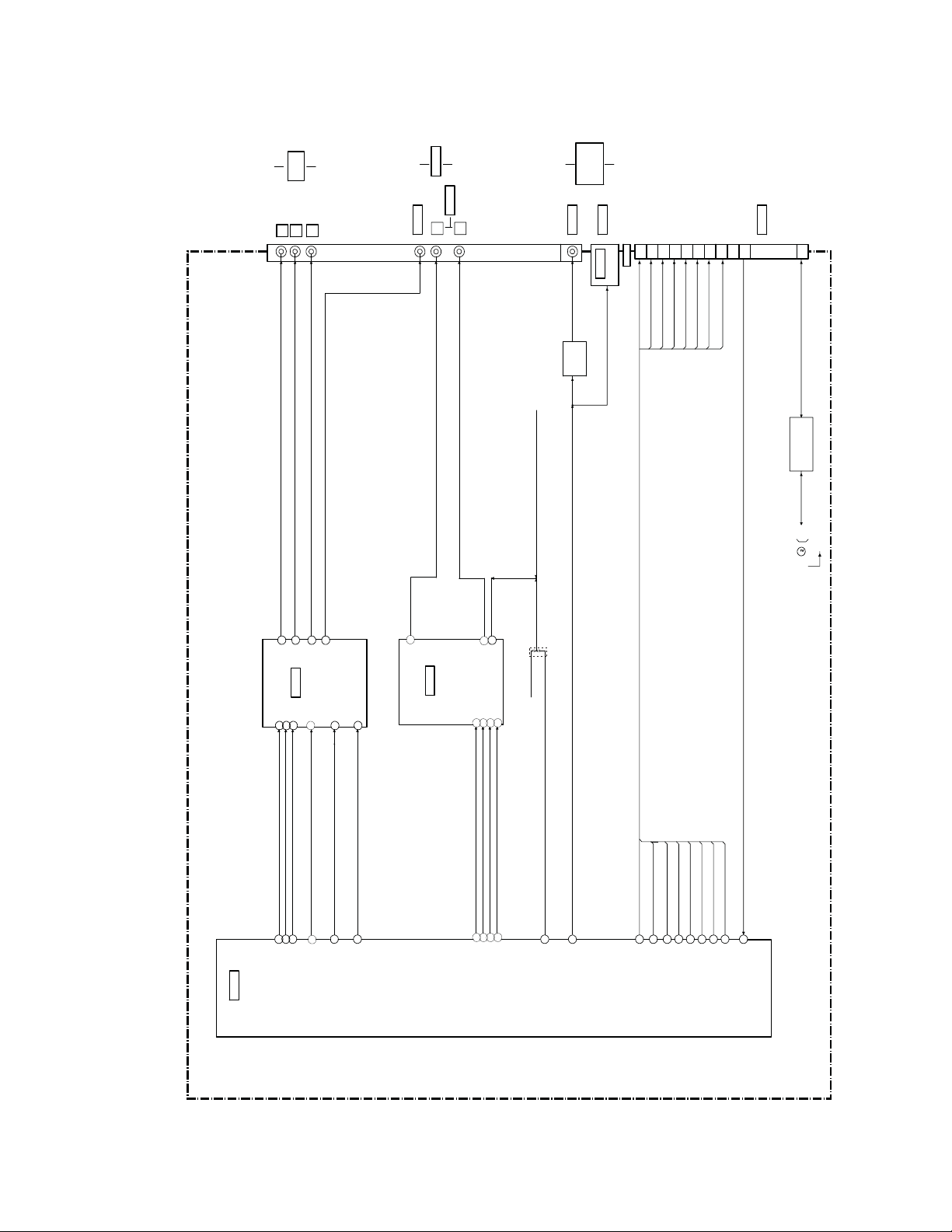
BDP-BX37/S270/S370/S373/S470
4
0
J9
VIDEO OUT
COMPONENT
B
Y
P
LINE OUT
DIGITAL
DIGITAL OUT
PCM/DTS/DOLBY
AUDIO
VIDEO
R
P
R
L
COAXIAL
02
9
J
Q909
BUFFER
OPTICAL
L
A
04
TIC
9
P
C
O
I
R
TTE
I
M
S
RAN
T
3
1
CN701
TMDS DATA2-
TMDS DATA2+
P
2
X
T
TX2N
6
4
7
TMDS DATA0+
TMDS DATA1-
TMDS DATA1+
TX1N
TX1P
TX0P
0
2
9
1
1
TMDS CLOCK-
TMDS DATA0-
TMDS CLOCK+
TX0N
TXKP
TXKN
HPD
9
1
HDMI OUT
CEC
3
1
DAC3.3VA
Q702
CEC PULL-UP
ISOLATING SWITCH
CEC
IT-CON
PG 3-4
3
5
1
1
1011
T
T
T
U
U
U
O
OUT
O
Y
B
VO
P
P
PR
P
M
3
A
00
O
1
E
C
I
D
I
V
N
N
I
N
N
RI
B
I
I
Y
V
P
P
5
7
3
1
Y
PB
CVBS
PR
0H14
3
2
3
B3
A3
C3
D3
DACOUT1
DACOUT3
DACOUT2
DACOUT6
01
1
C
I
E
T
U
M
8
XVMUTE
VIND6
D
H
D/
S
4
1
FORMAT1
5
1
G
VIND8
1
AOUTL
IC901
D/A CONVERTER
GG4899DXC/GG3899DXC
F/I BSU
F/I TENREHTE IMDH ,TUO V/A
LORTNOC YROMEM F/I ATAS
PSD ,LORTNOC METSYS NIAM
11
16
XMUTE
AOUTR
DACDAT
MCLK
LRCK
BCLK
8
7
9
10
3
2
2
3
B2
E2
C2
D2
AOBCK
AOMCK
AOLRCK
AOSDATA0
D901
XAMUTE
IFCON_XMUTE
0
H2
AMUTE
9
A1
SPDIF
P
2
X
T
6
D2
CH2_P
TX2N
6
B2
CH2_M
TX1P
7
C2
CH1_P
TX1N
7
A2
CH1_M
TX0P
8
D2
CH0_P
TX0N
8
B2
CH2_M
TXKP
9
C2
CLK_P
TXKN
9
A2
CLK_M
9
3
G
HTPLG
3-3
MB-134 BOARD
3-3. AV OUT BLOCK DIAGRAM
Page 32
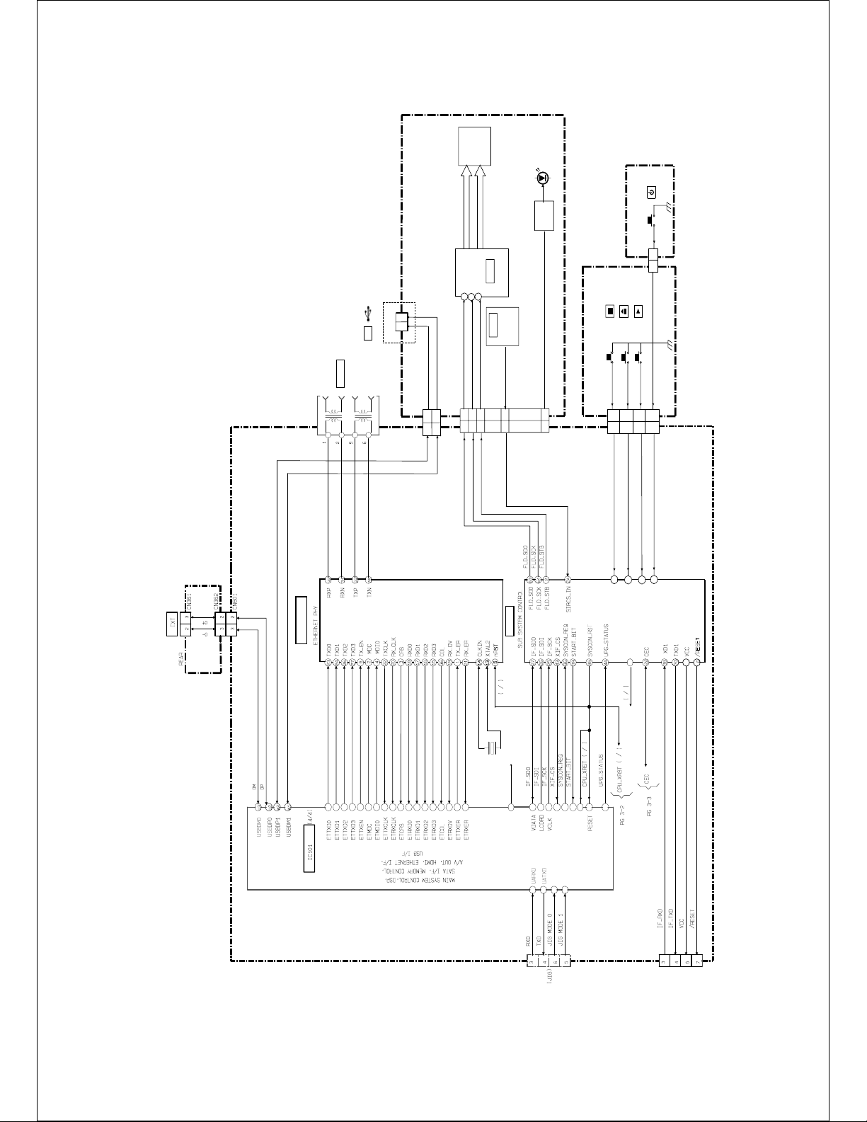
ND701
TUBE
INDICATOR
FLOURESCENT
D702
(WHITE)
BDP-BX37/S270/S370/S373/S470
CN1201
LAN (100)
USB
EXT
CN371
EXCEPT: BDP-S270
2
3
D+
FR-309 BOARD
CN372
FRONT
2
2
CN602
DP
S401
2
2
KEY1
S331
CN331
SWP-001 BOARD
CN401
S402
S403
3
4
345
KEY0
KEY2
KEY3
22
5
Q709
CONTROL
RECEIVER
LED DRIVER
6
6
SWB-001 BOARD
CN402
CN509
GRD1 - GRD8
SEG1 -SEG17
IC702
FL DRIVER
DIN
CLK
STB
798
IC701
REMOTE
D-
CN702
3
10811
13
10811
LED_CK
FLD_STB
13
SIRCS_IN
3
DM
CN1504
LED_DT
3-4
49
48
47
KEY0
KEY1
KEY246KEY3
X1201
25MHz
IC1503
3
2
Front end circuit
MRESET
CPU_PRERST
R
C35
2
1
3
1
C19
A17
C35
B34
A37
CN1102
AP4
G33
A35
D34
VSTB
GPIO2
GPIO1
CORE_RESETB
GPIO4
GPIO5
AW11
AY10
D36
CPU_PRERST
3
1
E35
AV12
GPIO6
10
CN1502
USB-023
BOARD
IC1201
C43
MB-134 BOARD
E39
F36
C41
H34
A41
C39
C37
D40
B38
D38
A43
B40
GG4899DXC/GG3899DXC
D42
B42
A39
E37
F38
3-4. USB/ETHER BLOCK DIAGRAM
Page 33
BDP-BX37/S270/S370/S373/S470
CN1503
EXT
USB
1
CN371
ND701
TUBE
INICATOR
FLUORESENT
DCDC
Q706,Q707
CONVERTER
EXT
USB
USB-023
CN362
CN601
CN361
1
4
4
USB 5V
CN701
HDMI OUT
8
1
HDMI 5V
CN602
CN372
Q703,Q704
B+ SWITCH
PS701
CN702
4
3-4
4
3-4
CN1504
FR_6V
FAN
M1501
(IFCON FLASH WRITER)
6
CN 1502
C
C
V
IF CON
IC 1503
L 3
AN CONTRO
FAN CONTROL 1
FAN CONTROL 2
F
Q501
Q502
FAN CONTROL 0
UNSW3.3V
PCONT2
PCONT3
PCONT4
A_PCONT
PCONT_CORE
AT
USB 5V
RECT
D705,D706
Q709
LED DRIVE
D702
LED WHITE
7
7
FLD_PCONT
LED_W
6
6
IT_3.3V
IC702
FL DRIVE
IC701
RECEIVER
REMOTE CONTROL
R708
FR-309 BOARD
1
1
V
3.3
SW
UN
A
V
5
W
S
IC 904
or d otte d li ne with ma rk
L
T
A
XI
P
O
COA
J902
CN1401
8V
3.3V
5V
IC 2301
DRIVER
MOTOR
3.3V
CN1102
NISECON
3.3V
ICE
8
1
CN1101
SW3.3V
are cr itical for s af ety.
mark
Replace only with part number
specifi ed.
The comp on en t s id en t i fi ed by
8
1
FAN
IC 1501
REGULATOR
IC104
DDR2
SDRAM
DDR2_1.8V
IC310
DC DC +1.8V
PCONT 1
MB-134 BOARD
IC105
VREF_0.9V
DDR2_VTT0.9V
0.9V
IC311
PS304
301
N
C
+3.3V
IC 301
DDR2
SDRAM
REGULATOR
PCONT4
IC 308
UNSW6V
1
REGULATOR
IC204
1
CPU1.2V
1.2V
IC303
V
4
C
D
C
D
DDR2
SDRAM
1
AVDD12_HDMI
+1.2V
REGULATOR
PCONT 2
PCONT3
IC205
1
CPU3.3V
3.3V
IC307
DDR2
SDRAM
+3.3V
REGULATOR
PCONT3
+5V
IC 601
REGULATOR
IC101
1
CORE_STB3.3V
IC1201
IC 502
USB_VBUS_PCONT1
1
CXD9983GG/CXD9984GG
PHY
ETHER
SERIAL
FLASH
IC 501
NAND
FLASH
+5V
IC 602
REGULATOR
1
CORE_STB1.1V
1.1V
IC309
DC DC CON
PCONT_CORE
UNSW6V
PS302
IC 705
USB_VBUS_PCONT2
1
1
AVDD33_HDMI
IC704
+3.3V
REGULATOR
PCONT3
978
+5V
REGULATOR
PCONT3
IC305
3.3V 1.2V
IC901
DAC 3.3 VA
+3.3V
REGULATOR
DAC
AUDIO
PCONT3
IC 304
VIDEO
IC1003
BUFFER
VIDEO BUFFER 3.3V
+3.3V
IC1001
REGULATOR
PCONT3
CN301
+5V
REGULATOR
IC1002
PS303
PCONT3
-5V
10
REGULATOR
PCONT2
FE_SW5V
IC 312
Q303
FE_SW5V
+5V
6
FE_SW3.3V
REGULATOR
ATA_PCONT
+8V
IC 1451
FE_SW12V
Q302
FE-UNSW 12V
PS301
2
IC 2401
REGULATOR
MOTOR
DRIVER
3-5E
UNSW12V
1
1
2
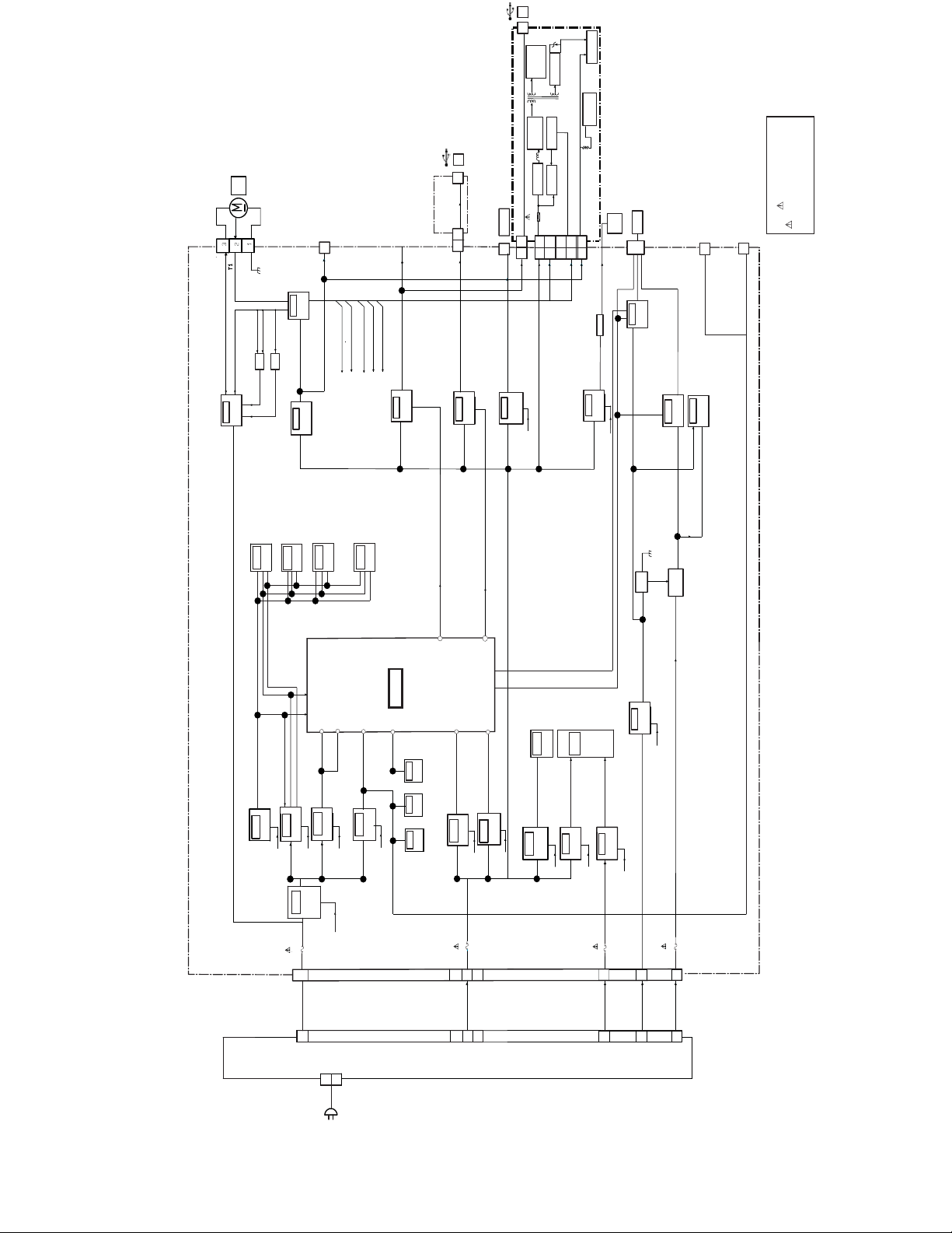
3-5. PO W ER BLOC K D IAGRAM
(AC IN)
UNSW6V
UNSW-6V
FE-UNSW-6V FE-UNSW6V
0
978
SRV2206UC(BDP-BX37/S270/S370:US,CND,MX/S470:US,CND)
APS-257(BDP-S370:EXCEPT(US,CND,MX)/S373/S470:EXCEPT (US,CND))
1
SWITCHING REGULATOR :
FE-UNSW 12V
2
6
Page 34
SECTION 4
SCHEMATIC DIAGRAMS
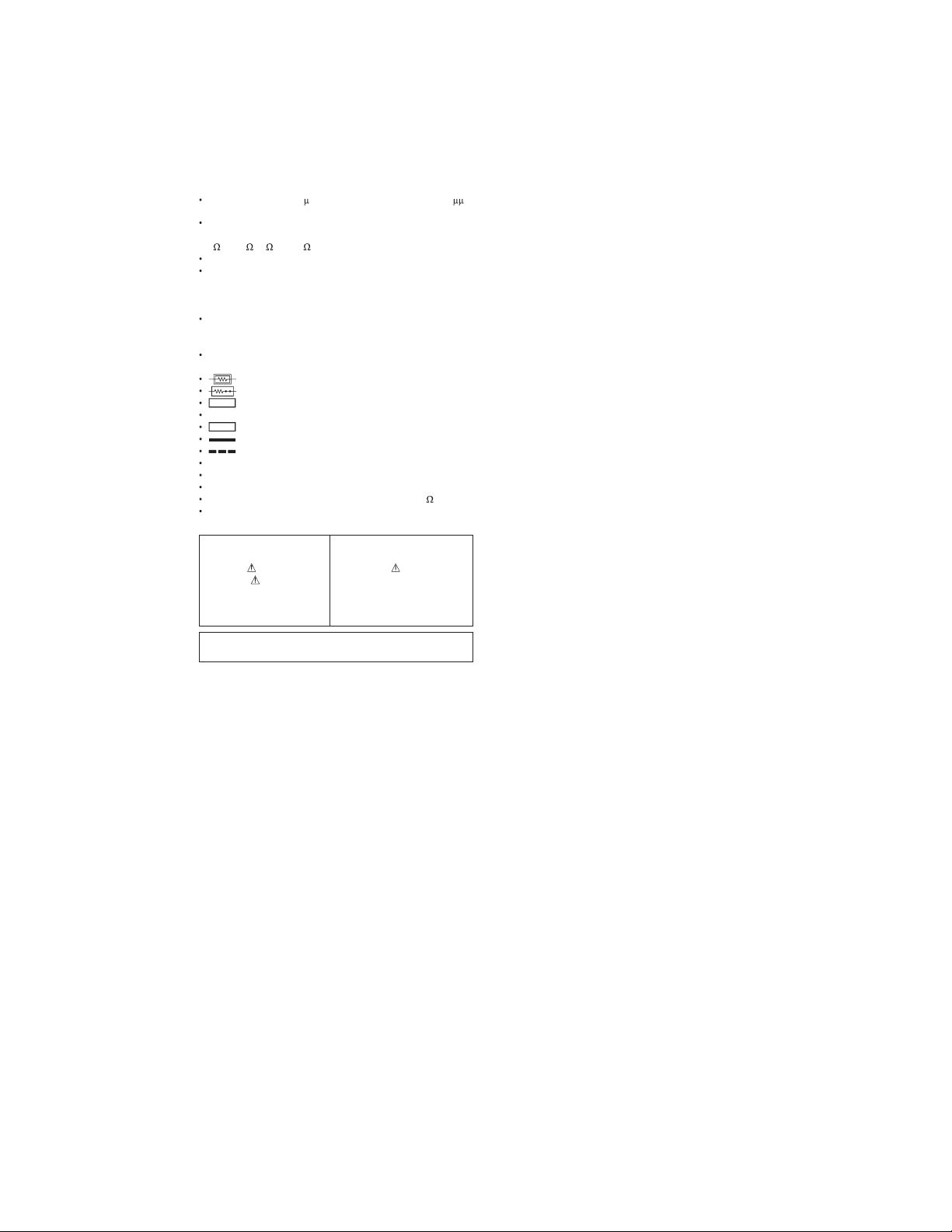
4-1. THIS NOTE IS COMMON FOR SCHEMATIC DIAGRAMS
All capacitors are in F unless otherwise noted. pF : F.
50V or less are not indicated except for electrolytics and tantalums.
All resistors are in ohms, 1/4 W (Chip resistors : 1 /10 W) un-less
otherwise specified.
k
=1000 , M =1000k .
% : indicates tolerance.
Caution when replacing chip parts.
New parts must be attached after removal of chip.
Be careful not to heat the minus side of tantalum capacitor, because
it is damaged by the heat.
Constants of resistors, capacitors, ICs and etc with XX indicate
that they are not used.
In such cases, the unused circuits may be indicated.
All variable and adjustable resistors have characteristic curve B,
unless otherwise noted.
: nonflammable resistor
: fusible resistor
: panel designation
f : internal component.
: adjustment for repair.
: B+ Line
: B– Line
Circled numbers refer to waveforms.
Voltages are dc between measurement point.
Readings are taken with a color-bar signals on Blu-ray disc.
Readings are taken with a digital multimeter (DC 10M ).
Voltage variations may be noted due to normal production tolerances.
B DP-BX37/S270/S370/S373/S470
Note:
The components identified
by mark
with mark
safety.
Replace only with part number specified.
When indicating parts by reference number, please include the
board name.
or dotted line
are critical for
Note:
Les composants identifiés par
une marque
pour la sécurité.
Ne les remplacer que par une
pièce portant le numéro spécifié.
sont critiquens
4-1
Page 35
14
13
BDP-BX37/S270/S370/S373/S470
12
11
10
98765
EXCEPT US,CND
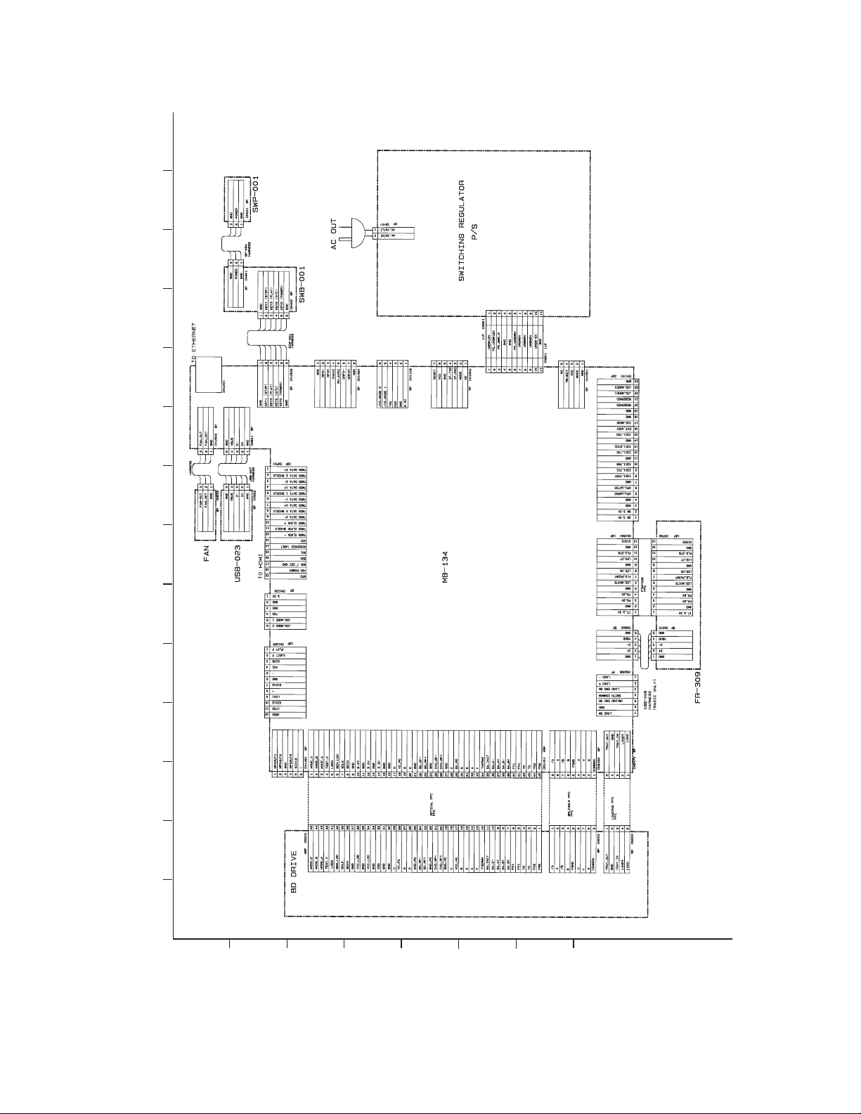
APS-257(S370:EXCEPT (US,CND,MX)/S373/S470:
SRV2206UC(BDP-BX37/S270/S370:US,CND,MX/S470:US,CND
4-2
43
2
AAA064-MEK
1
A
B
C
D
E
F
G
H
I
J
FRAME SCHEMATIC DIAGRAM
4-2.
Page 36
BDP-BX37/S270/S370/S373/S470
14
3.7
-16.2
13
12
-18.7
-18.7
-18.7
-18.7
-18.7
-18.7
-18.7
-18.7
3.3
-18.5
-9
-1
-21
-21
-13.7
-21.4
-21
-13.6
-13.6
-11.5
-11.2
-20.9
-21
-21
-11.1
-18.5
3.3
3
2.6
0.1
1.9
are critical for safety.
Replace only with part number
mark
by mark or dotted line with
11
10
98765
4-3
0.1
3.3
WHITE LED CIRCUIT
43
2
1
A
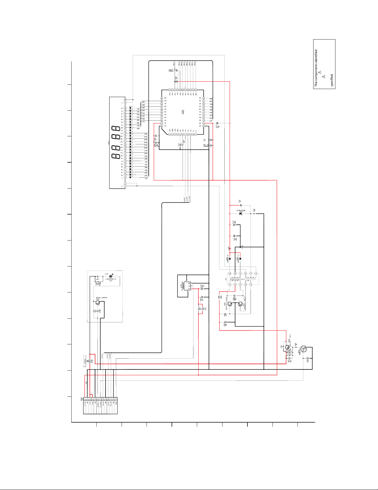
- Ref. No.: FR-309 board; 20,000 series -
4-3. FR-309 BOARD (FRONT RIGHT) SCHEMATIC DIAGRAM • See p a ge 5 - 3 for printe d wiring boa rd.
3.3
3.3
5.6
5.6
0
0
5.6
0.1
4.9
5.7
3.3
B
C
D
E
F
G
H
I
J
Page 37
BDP-BX37/S270/S370/S373/S470
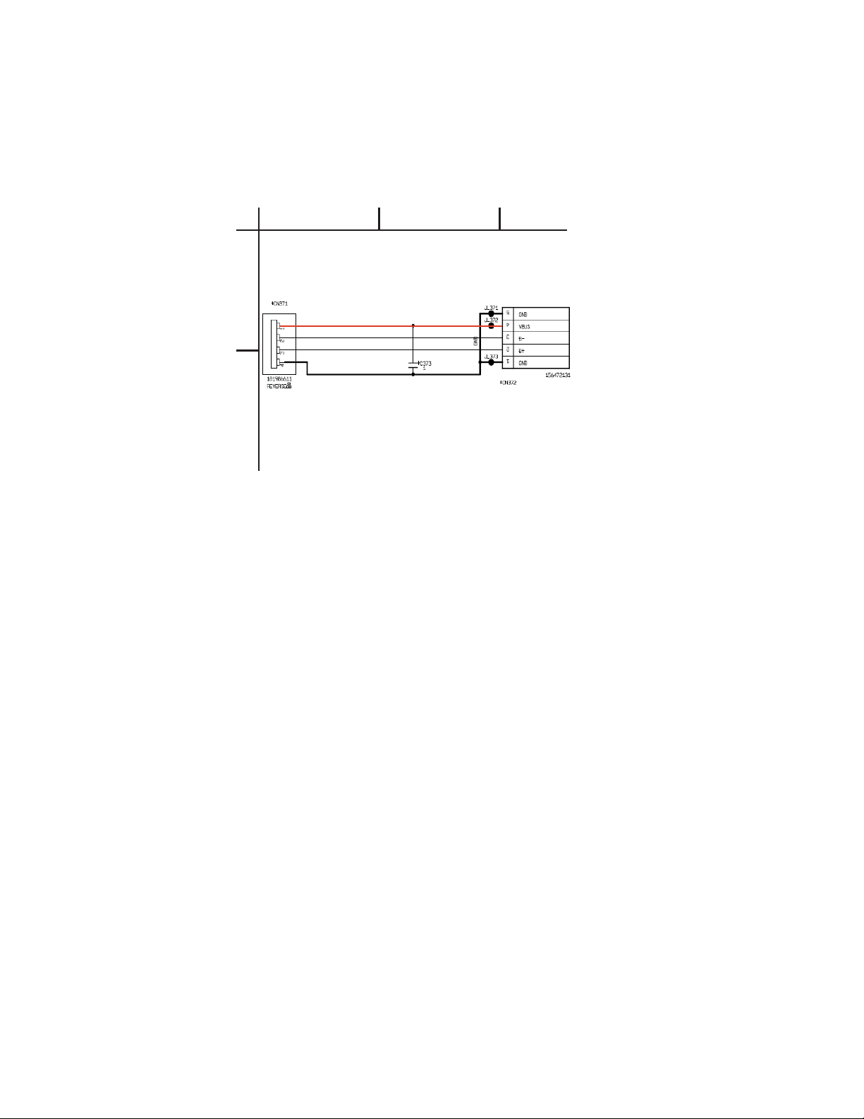
4-4. FR-309 BOARD (USB FRONT) SCHEMATIC DIAGRAM
- Ref. No.: FR-309 board; 20,000 series -
• See page 5-3 for printed wiring board.
FR-309 BOARD
A
USB
B
2
5
31
4-4
Page 38
14
13
BDP-BX37/S270/S370/S373/S470
12
11
10
98765
4-5
43
2
1
A
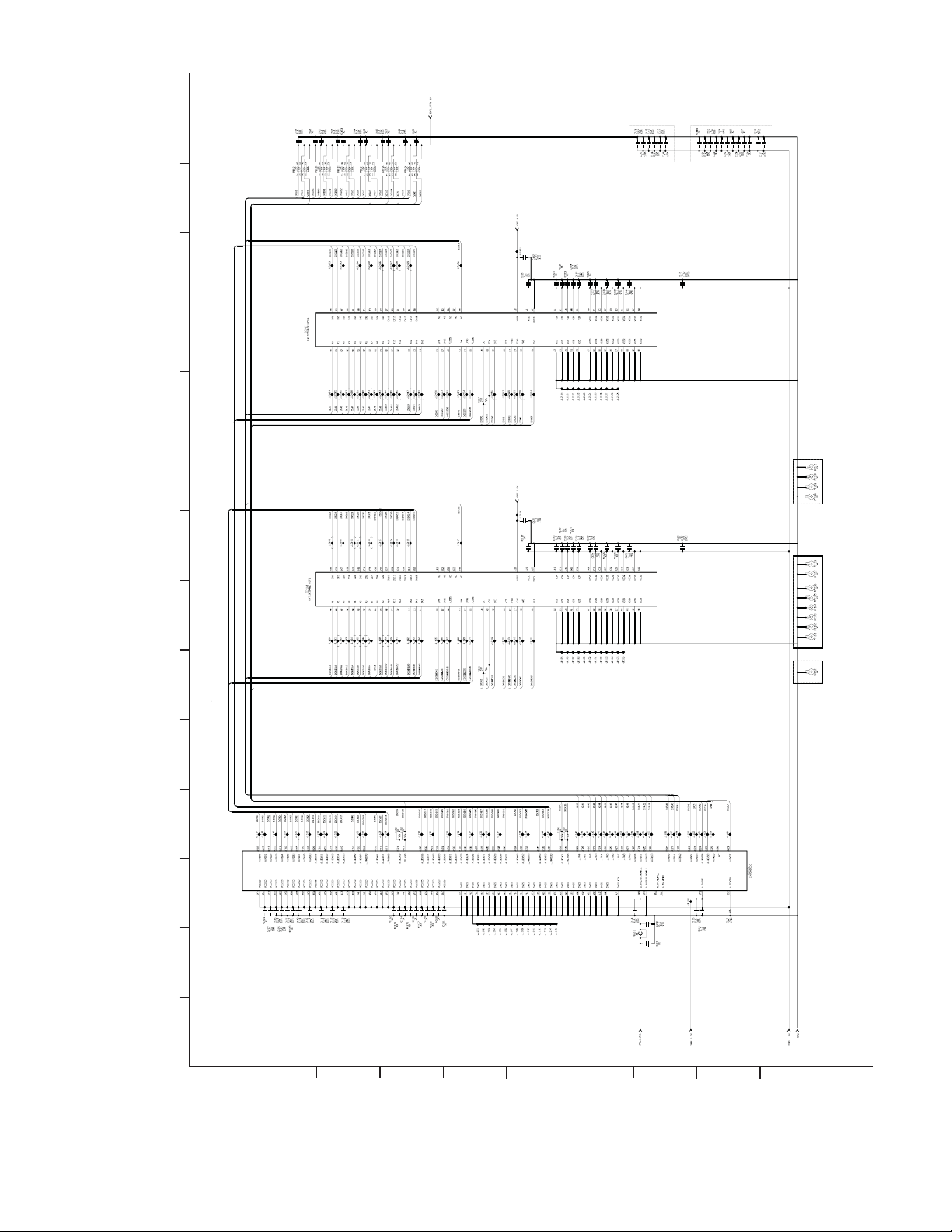
4-5. MB-134 BOARD (CXD9983GG/9984GG) SCHEMATIC DIAGRAM (1/15) • See page 5-4 for printed wiring board.
- Ref. No.: MB-134 board; 10,000 series
B
C
D
E
F
G
H
I
J
Page 39
14
13
BDP-BX37/S270/S370/S373/S470
12
11
10
98765
4-6
43
2
1
A
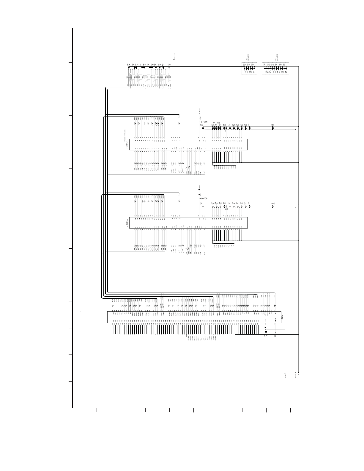
4-6. MB-134 BOARD (CXD9983GG/9984GG) SCHEMATIC DIAGRAM (2/15) • See page 5-4 for printed wiring board.
- Ref. No.: MB-134 board; 10,000 series
B
C
D
E
F
G
H
I
J
Page 40
or dotted line with
are c ritical fo r s a f ety.
14
mark
The components identifi ed
by mark
Replace only with part number
specifi ed.
BDP-BX37/S270/S370/S373/S470
13
12
11
10
98765
1.8
3.7
0.9
1
8.1
11.8
1.8
1.1
1.1
5.7
5.7
3.3
1.8
3.3
0.9
1.8
11.9
11.9
5.0
0
8.0
0
5.0
3.3
5.8
4-7
• S e e pa ge 5 - 4 for printe d wiring boa rd.
0
1.2
0
5.0
5.8
3.3
3.7
3.3
43
2
1
A
- Ref. No.: MB-134 board; 10,000 series -
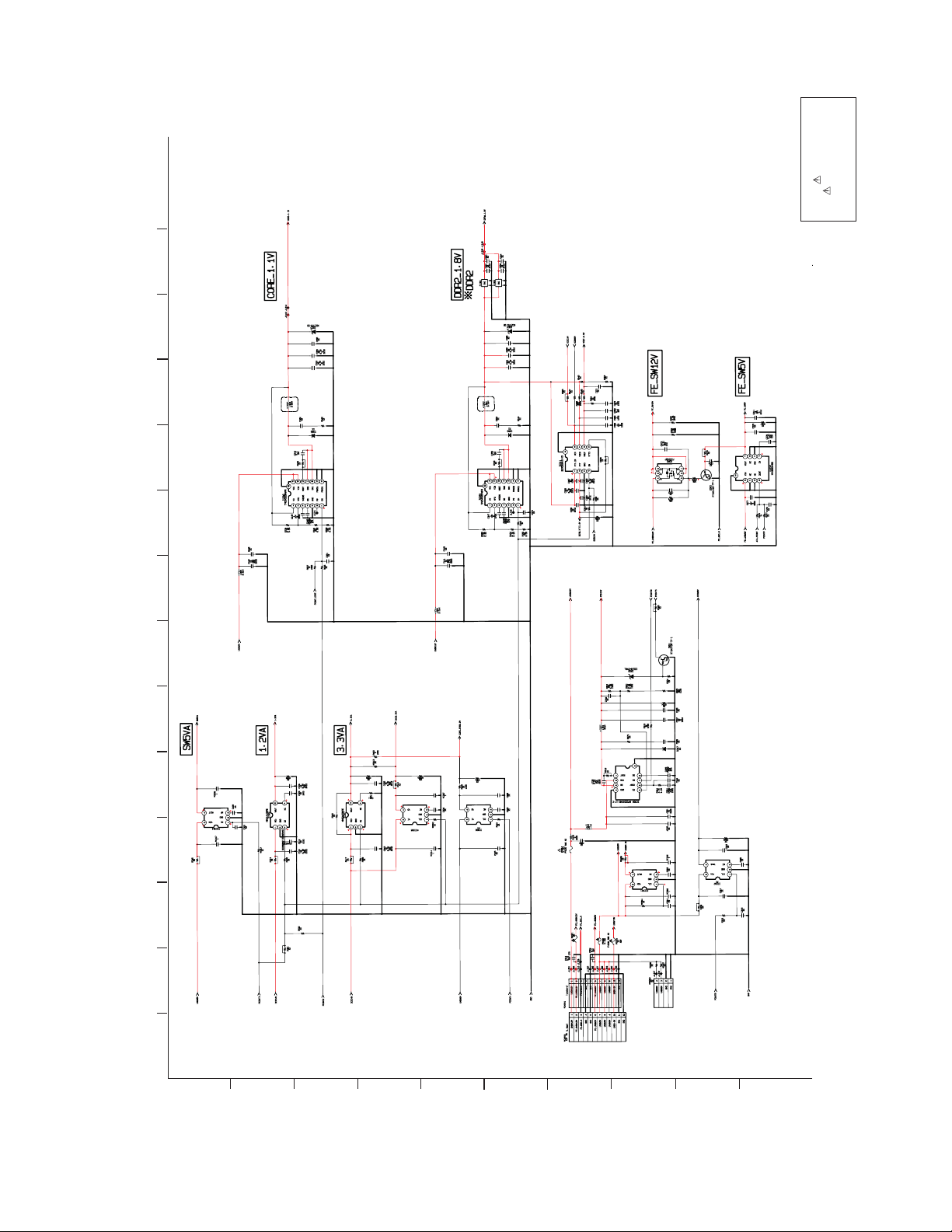
4-7. MB-134 BOARD (POWER1) SCHEMATIC DIAGRAM (3/15)
B
11.8
3.3
0
3.3
0
3.7
3.3
3.7
C
3.3
D
E
F
3.8
3.3
0
1.8
5.8
G
H
I
J
Page 41
14
13
BDP-BX37/S270/S370/S373/S470
12
11
10
98765
4-8
43
2
1
A
- Ref. No.: MB-134 board; 10,000 series -
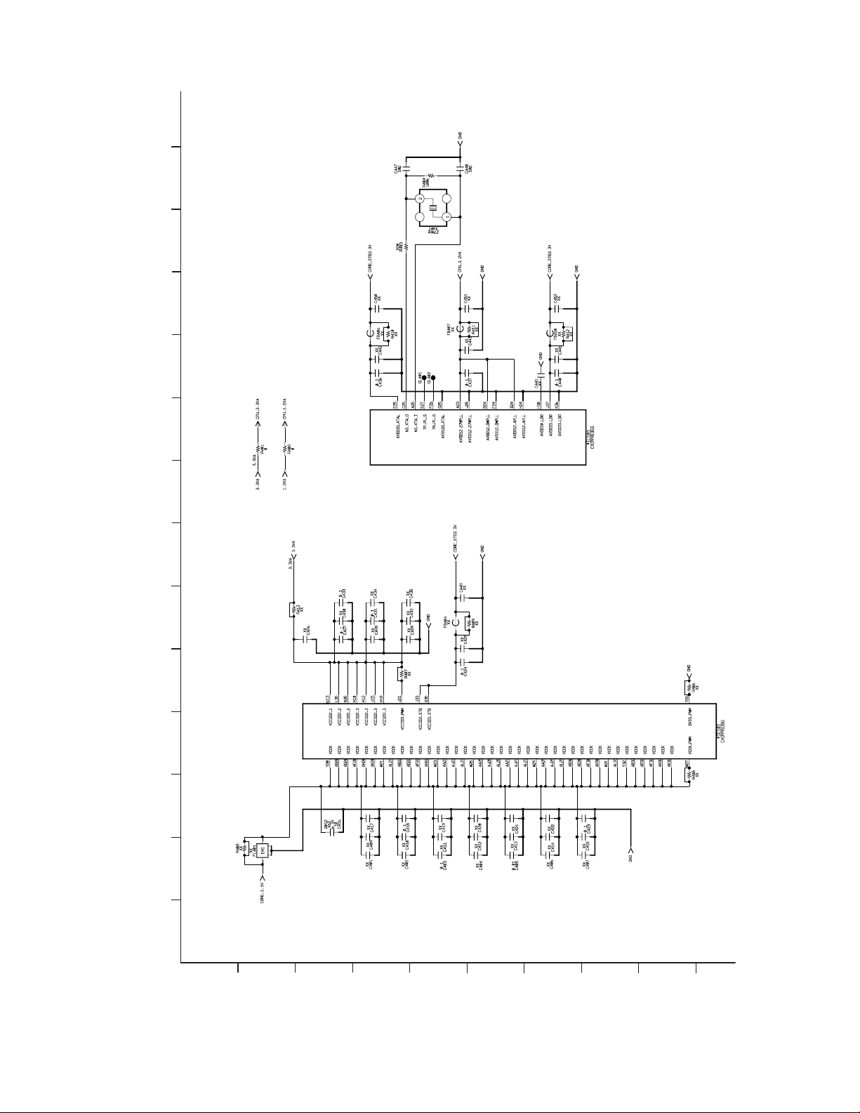
4-8. MB-134 BOARD (CLK/POWER2) SCHEMATIC DIAGRAM (4/15) • See page 5-4 for printed wiring board.
B
C
D
E
F
G
H
I
J
Page 42
14
BDP-BX37/S270/S370/S373/S470
13
12
0
3.3
*
*
3.3
*
*
3.3
11
10
98765
***
***
*
3.3
0
*
4-9
***
***
*
• S e e pa ge 5 - 4 for printe d wiring boa rd.
43
2
1
A
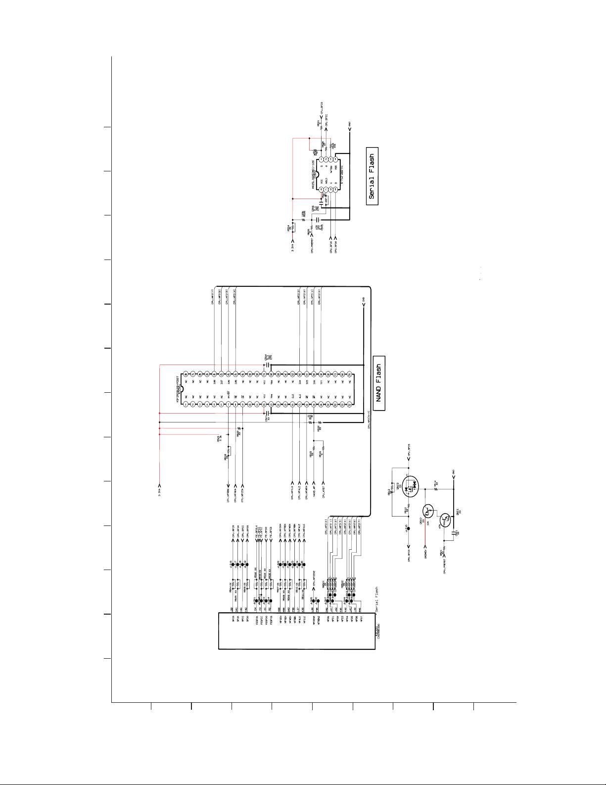
4-9. MB-134 BOARD (FLASH/HOST) SCHEMATIC DIAGRAM (5/15)
- Ref. No.: MB-134 board; 10,000 series -
B
C
D
E
F
G
H
I
J
Page 43
BDP-BX37/S270/S370/S373/S470
14
13
12
11
10
98765
• S e e pa ge 5 -4 for printe d wiring boa rd.
5
5.8
5
5.8
EXCEPT BDP-S270
4-10
43
2
1
A
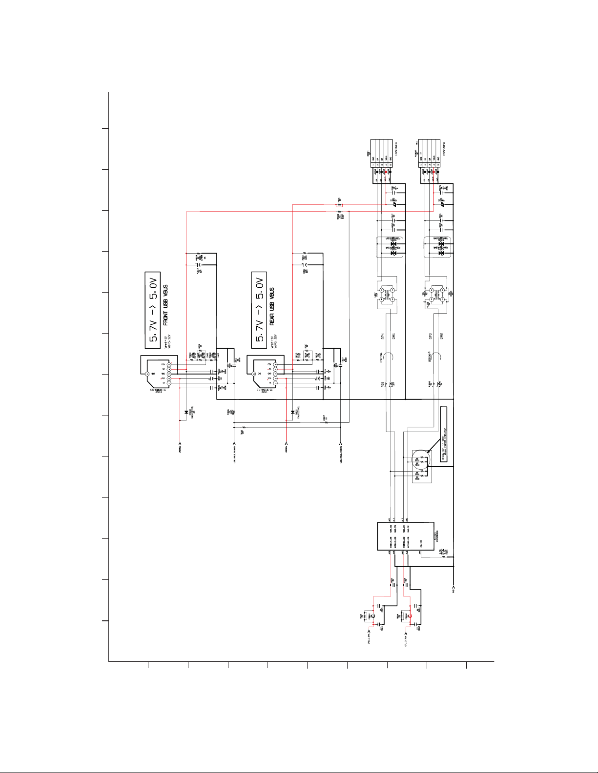
4-10. MB-134 BOARD (USB) SCHEMATIC DIAGRAM (6/15)
- Ref. No.: MB-134 board; 10,000 series -
B
C
D
E
F
G
H
I
J
Page 44
BDP-BX37/S270/S370/S373/S470
14
13
12
11
3.3
5.8
3.3
10
98765
4-11
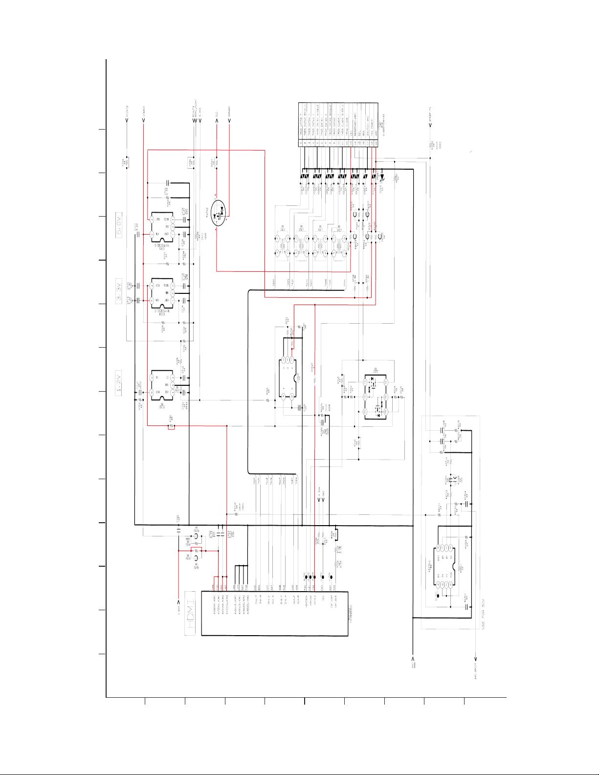
• S e e pa ge 5 - 4 for printe d wiring boa rd.
43
2
1
A
4-11. MB-134 BOARD (HDMI) SCHEMATIC DIAGRAM (7/15)
- Ref. No.: MB-134 board; 10,000 series -
B
C
D
E
F
G
H
I
J
Page 45
BDP-BX37/S270/S370/S373/S470
14
13
12
11
10
98765
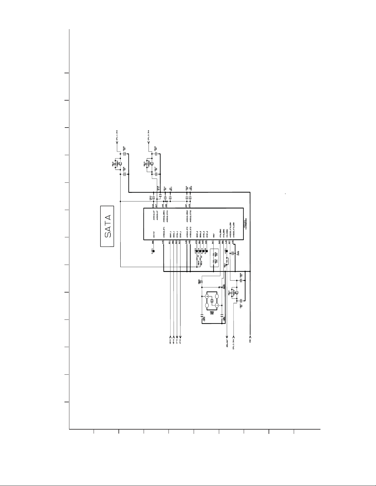
• Se e pa ge 5 - 4 for printe d wiring boa rd.
4-12
43
2
1
A
- Ref. No.: MB-134 board; 10,000 series -
4-12. MB-134 BOARD (SATA) SCHEMATIC DIAGRAM (8/15)
B
C
D
E
F
G
H
I
J
Page 46
BDP-BX37/S270/S370/S373/S470
14
5
1.6
13
12
5
1.8
2.5
11
10
98765
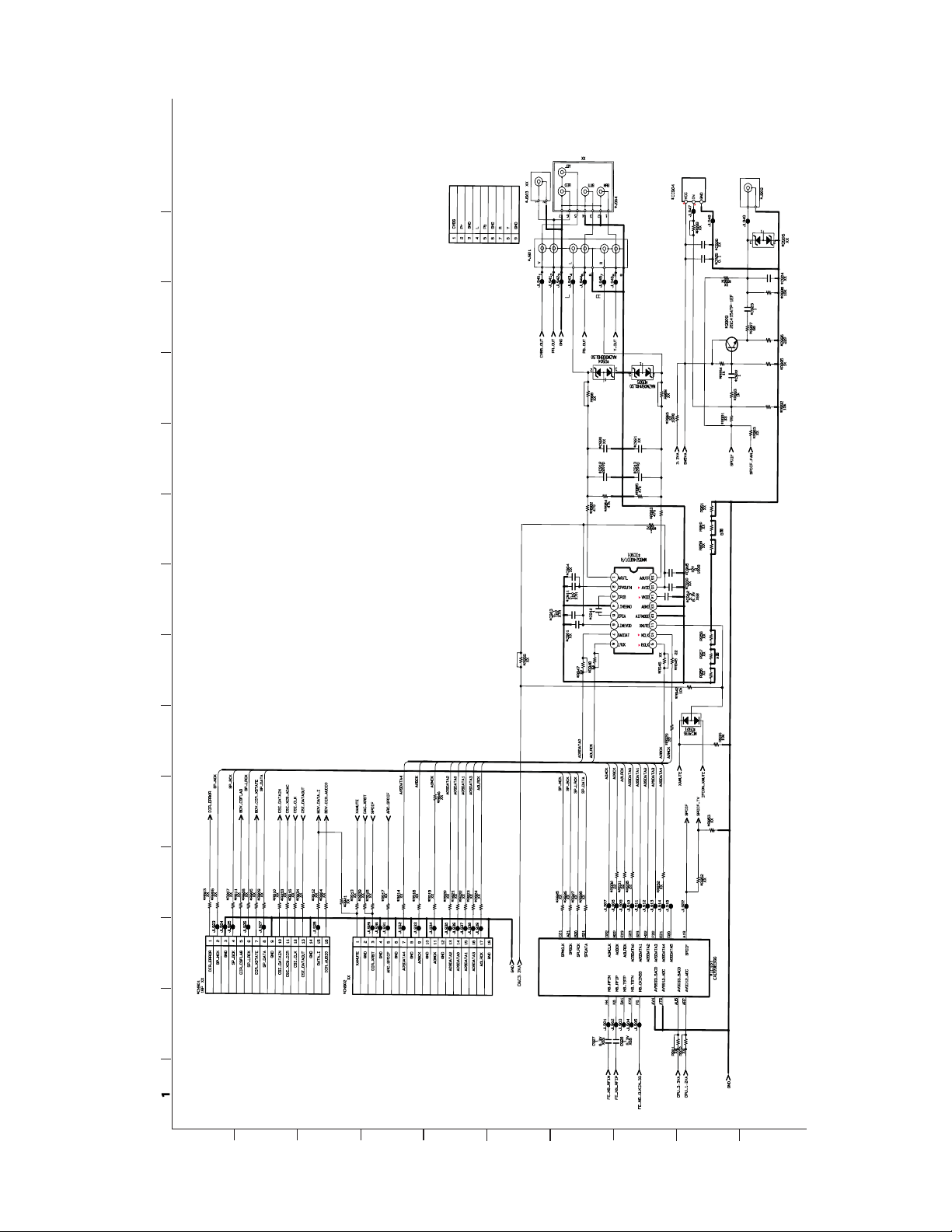
for printed wiring boa rd.
5-4
• See page
0
3.3
1.6
1.8
1.65
playback)
(only during
3.3
playback)
3.3
3.3
(only during
4-13
)kcabyalp gnirud ylno( 56.1
0
3.3
6.1-
7.1
3.3
1.65
43
2
1
A
4-13. MB-134 BOARD (AUDIO) SCHEMATIC DIAGRAM (9/15)
- Ref. No.: MB-134 board; 10,000 series -
B
C
D
E
F
G
H
I
J
Page 47
14
13
BDP-BX37/S270/S370/S373/S470
12
11
10
98765
6
5
8
000
3.3
0
0.3
0.7
1
4
0.7
3.3
7
0
0
-5
0.3
3.3 -5
2
3
4-14
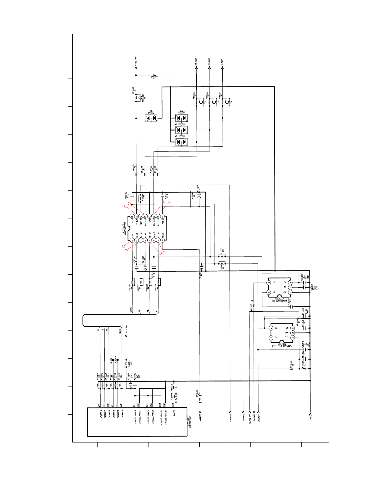
• Se e pa ge 5 - 4 for printe d wiring boa rd.
43
2
1
A
- Ref. No.: MB-134 board; 10,000 series -
4-14. MB-134 BOARD (VIDEO) SCHEMATIC DIAGRAM (10/15)
3.3
0
3.3
0.6
B
C
D
E
F
G
H
-5
0.6-
0
3.3
I
J
Page 48
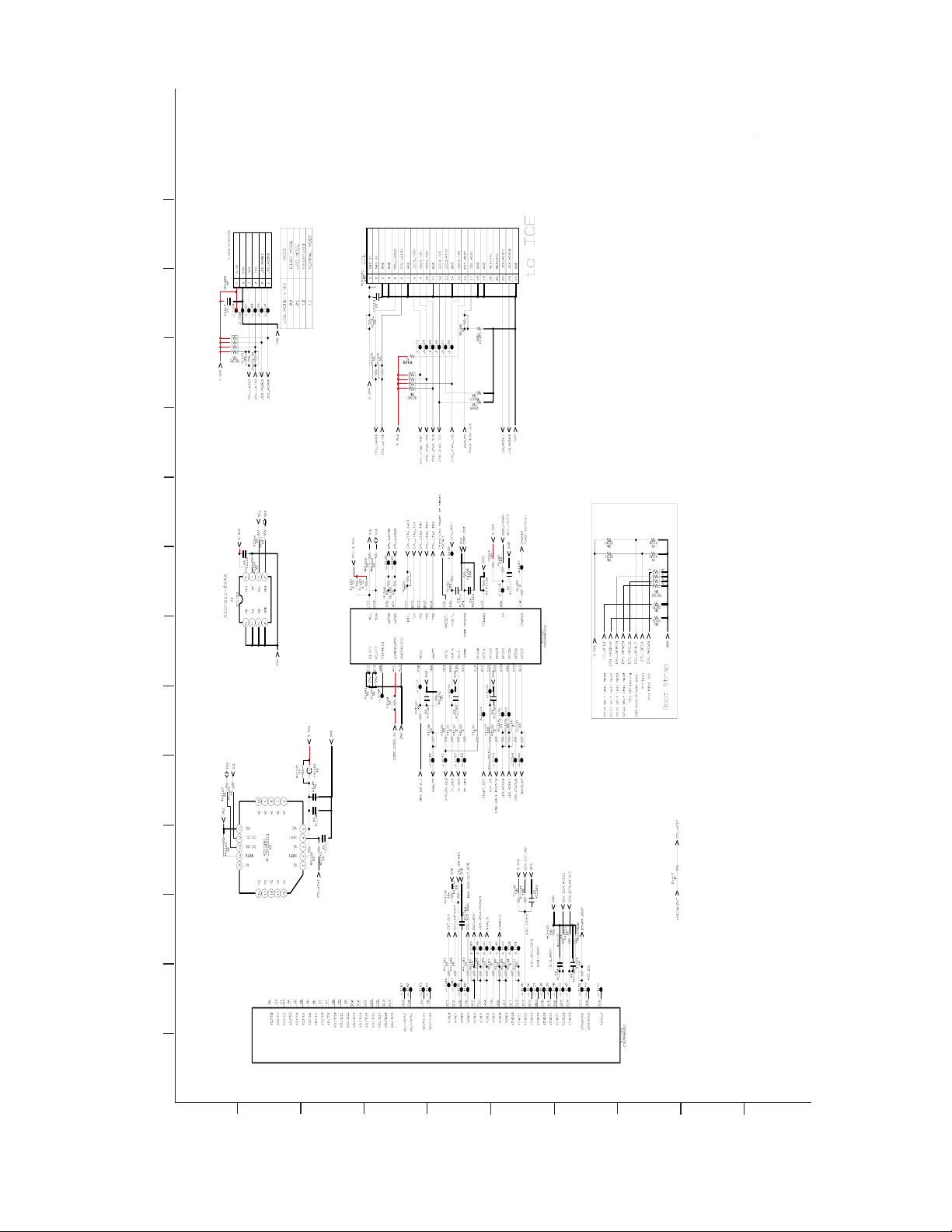
BDP-BX37/S270/S370/S373/S470
14
13
12
11
10
98765
• Se e p a ge 5 - 4 for printed wiring boa rd.
4-15
43
2
1
A
4-15. MB-134 BOARD (GPIO/JTAG) SCHEMATIC DIAGRAM (11/15)
- Ref. No.: MB-134 board; 10,000 series -
B
C
D
E
F
G
H
I
J
Page 49
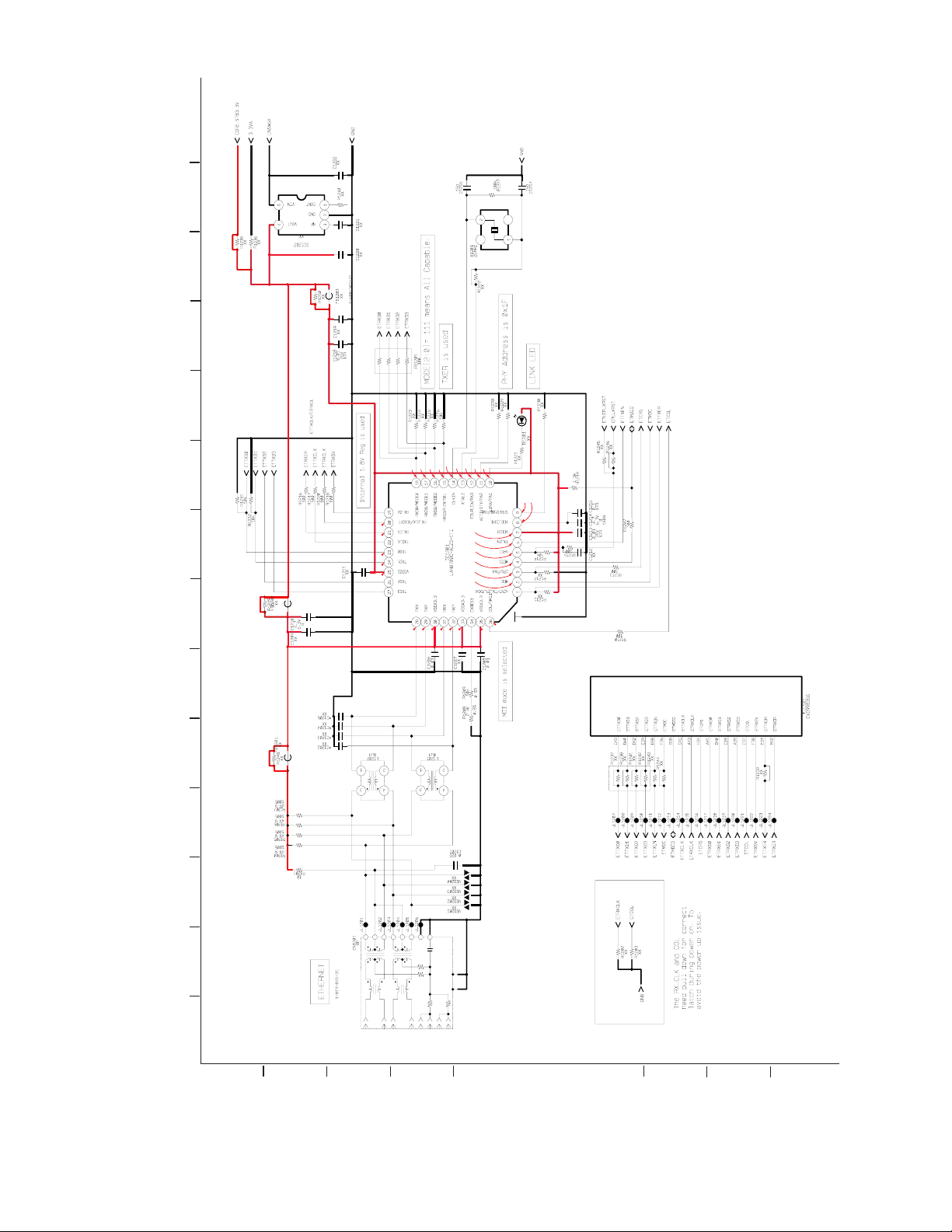
14
13
BDP-BX37/S270/S370/S373/S470
12
11
10
2.0
0
000
000
***
3.3
2.1
0
3.3
3.3
3.3
*** *
*
*
3.3
3.3
4-16
98765
0
0
300
• S e e p a ge 5- 4 for printe d wiring boa rd.
43
2
1
A
- Ref. No.: MB-134 board; 10,000 series -
4-16. MB-134 BOARD (ETHERNET) SCHEMATIC DIAGRAM (12/15)
B
C
D
E
F
G
H
I
J
Page 50
BDP-BX37/S270/S370/S373/S470
TO B/E
14
13
12
11
10
1.2
3.3
3.3
1.2
1.2
98765
• S e e p a ge 5 -4 for printe d wiring boa rd.
12
12
43
2
1
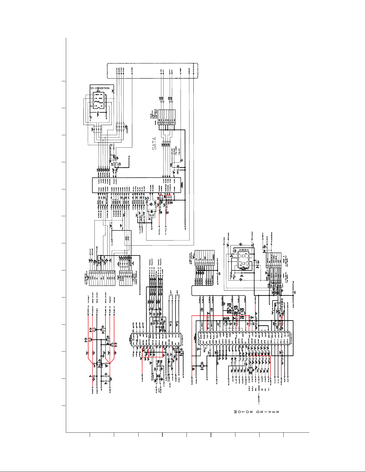
- Ref. No.: MB-134 board; 10,000 series -
A
4-17. MB-134 BOARD (FE_POWER/SF/SATA) SCHEMATIC DIAGRAM (13/15)
4-17
5
5
5
5
12
12
5
5
5
5
12
1.4
1.4
1.4
1.4
5
5
1.4
1.4
1.4
POWER (12V;5V)
B
C
POWER (3.3V;1.2V);
MOTOR DRIVER (SA)
D
E
F
G
H
I
J
Page 51
BDP-BX37/S270/S370/S373/S470
14
13
12
11
3.3
3.3
3.3
3.3
3.3
3.3
3.3
3.3
3.3
3.3
1.2
1.2
1.2
1.2
3.3
1.2
1.2
1.2
1.2
1.2
1.2
3.3
3.3
10
1.4
98765
4-1 8
8
43
2
1
A
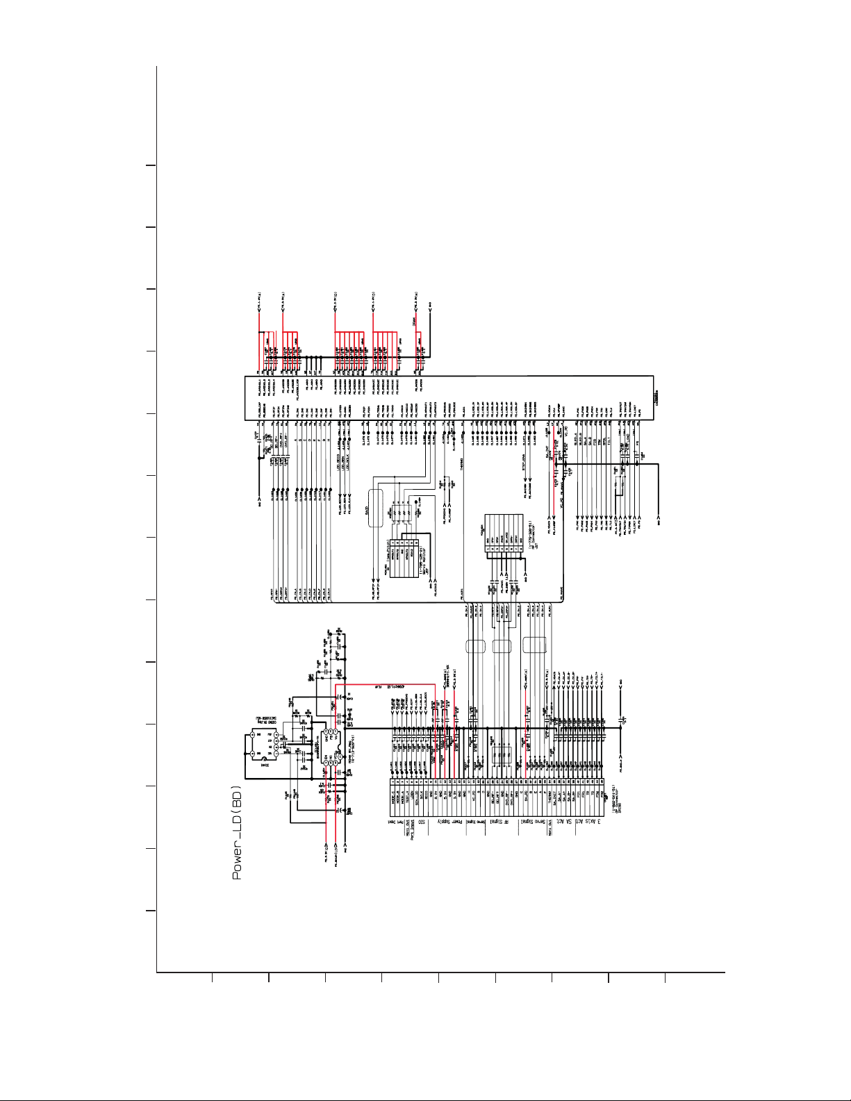
- Ref. No.: MB-134 board; 10,000 series -
• S e e p a ge 5 -5 for printe d wiring boa rd.
4-18. MB-134 BOARD (FE_OP/MOTOR DRIVE) SCHEMATIC DIAGRAM (14/15) • See page 5-4 for printed wiring board
B
5
12
3.3
C
D
8
3.3
E
F
5
G
H
I
J
Page 52
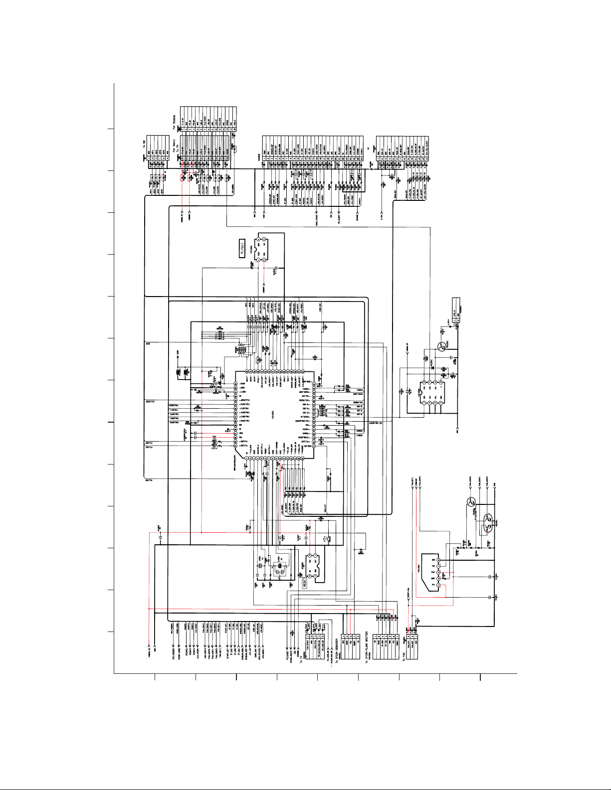
14
13
BDP-BX37/S270/S370/S373/S470
12
11
10
98765
5.7
3.3
3.3
3.3
3.3
3.3
3.300
0.2
3.3
3.3
3.3
3.3
.42
0
3.3
0
3.3
3.3
0
0
3.3
3.3
0
3
3.2
3.1
0
3.3
0
3.2
3.3
3.3
3.3
0
0
3.2
.33
3.3
3.2
.23
4-19
Se e page 5 - 4 for printed wiring board.
•
43
2
1
A
- Ref. No.: MB-134 board; 10,000 series -
4-19. MB-134 BOARD (IFD) SCHEMATIC DIAGRAM (15/15)
0
0
0 0 0
12
B
C
D
E
F
G
H
I
J
Page 53
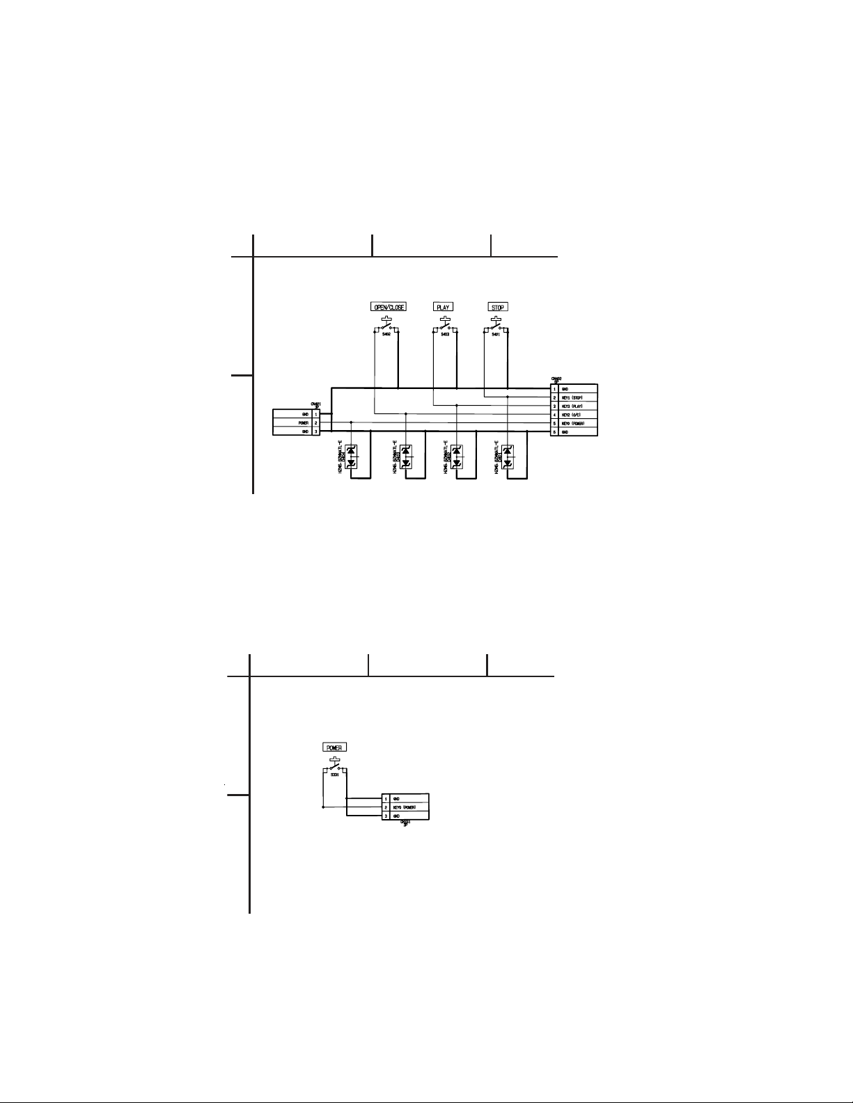
BDP-BX37/S270/S370/S373/S470
4-20. SWB-001 BOARD SCHEMATIC DIAGRAM
- Ref. No.: SWB-001 board; 20,000 series -
• See page 5-2 for printed wiring board.
2
SWB-001 BOARD
A
B
4-21. SWP-001 SCHEMATIC DIAGRAM
- Ref. No.: SWP-001 board; 20,000 series -
• See page 5-2 for printed wiring board.
31
SWP-001 BOARD
A
B
2
4- 20
31
Page 54
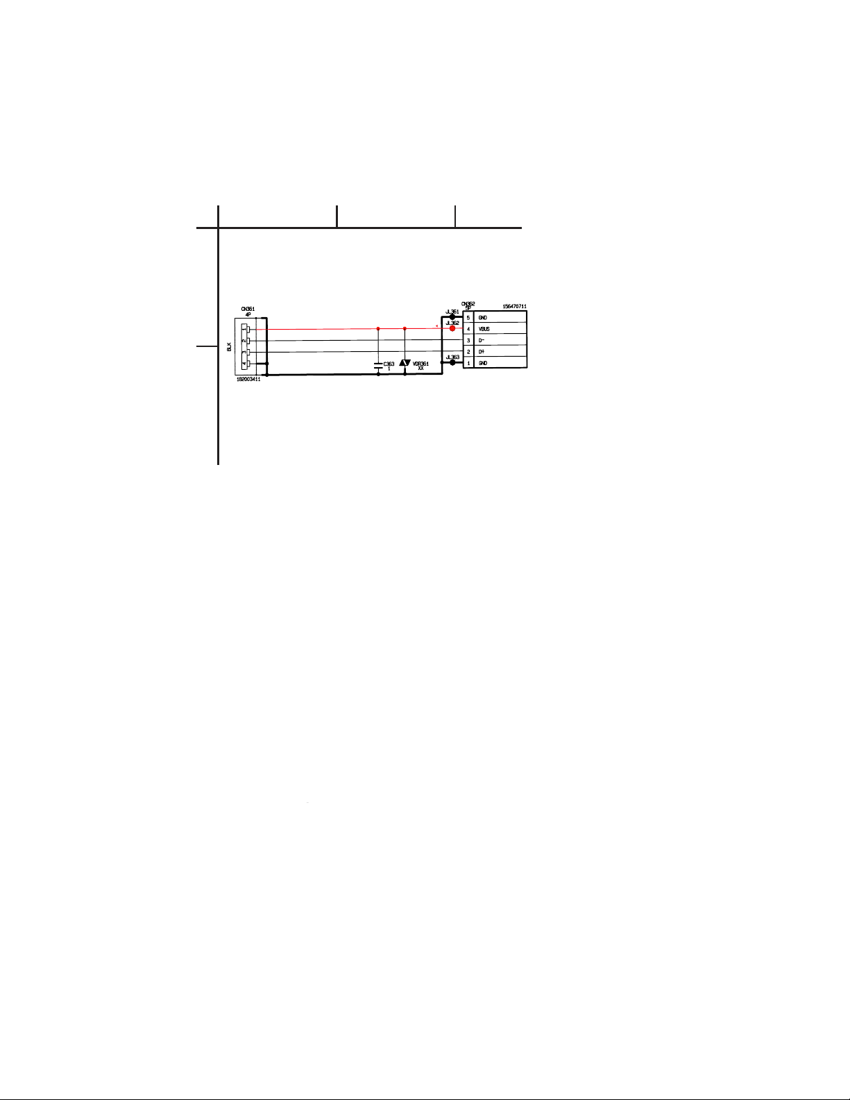
BDP- BX37/S270/S370/S373/S470
4-22. USB-023 (USB (REAR)) SCHEMATIC DIAGRAM
- Ref. No.: USB-023 board; 20,000 series -
• See page 5-6 for printed wiring board.
USB-023 BOARD
A
B
2
5
31
4-21
Page 55
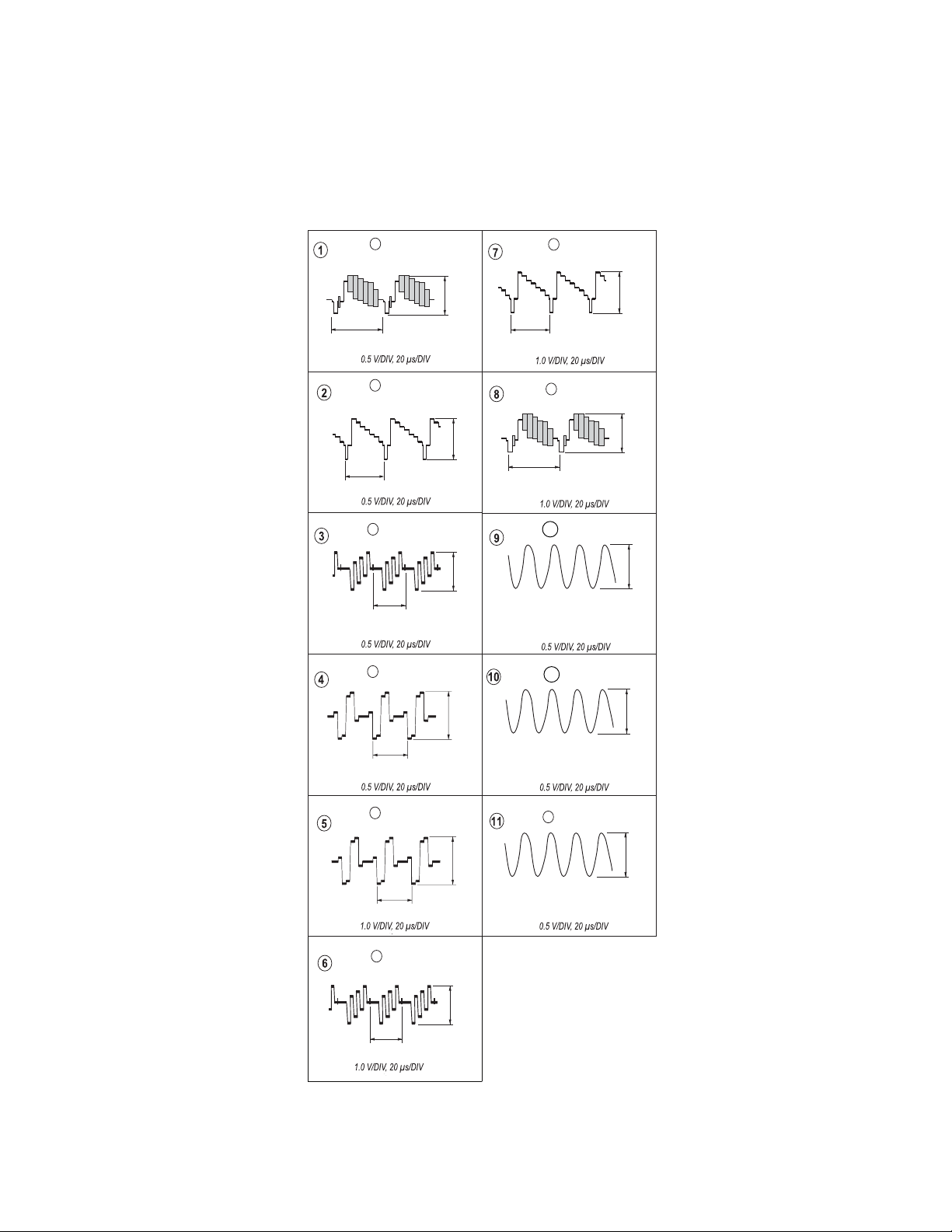
4-23. W AVEFORMS
MB-134 BOARD
IC1003
1
BDP-BX37/S270/S370/S373/S470
(VIN)IC1003
IC1003
(YOUT)
10
H
IC1003
IC1003
IC1003
(VOUT)
15
A25
(NS_XTAL_I)
(XTAL25MI)
BB8
2.0Vp-p
2.4Vp-p
Vpp
3.3 Vp-p
Vpp
2.1 Vp-p
1.2Vp-p
7
(PYIN)
(PBIN)
H
(PRIN)
H
1.0Vp-p
0.7Vp-p
0.7Vp-p
H
5
3
H
IC1003
H
IC101
27 MHz
IC101
25 MHz
IC1003
IC1003
13
(PROUT)
11
(PBOUT)
H
14
(CLKIN)
IC1201
Vpp
1.4Vp-p
H
1.4Vp-p
25 MHz
2.0 Vp-p
4-22E
Page 56
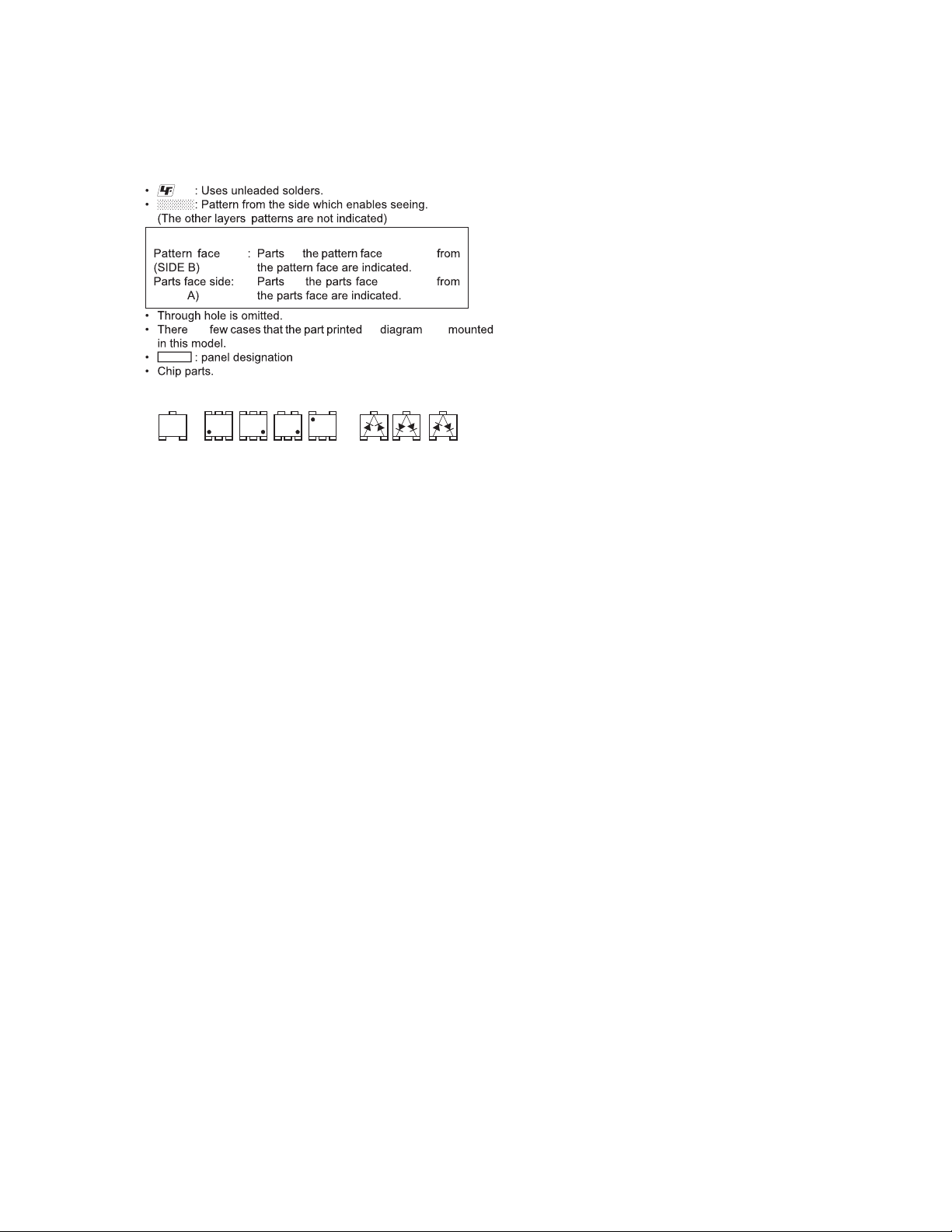
BDP-BX37/S270/S370/S373/S470
SECTION 5
PRINTED WIRING BOARDS
5-1. THIS NOTE IS COMMON FOR PRINTED WIRING BOARDS
’
Caution:
side
on side seen
(SIDE
are on isn’t
Transistor Diode
5
5246
EBC31
on side seen
654
123
21
54
345
123
3
21321321
Page 57
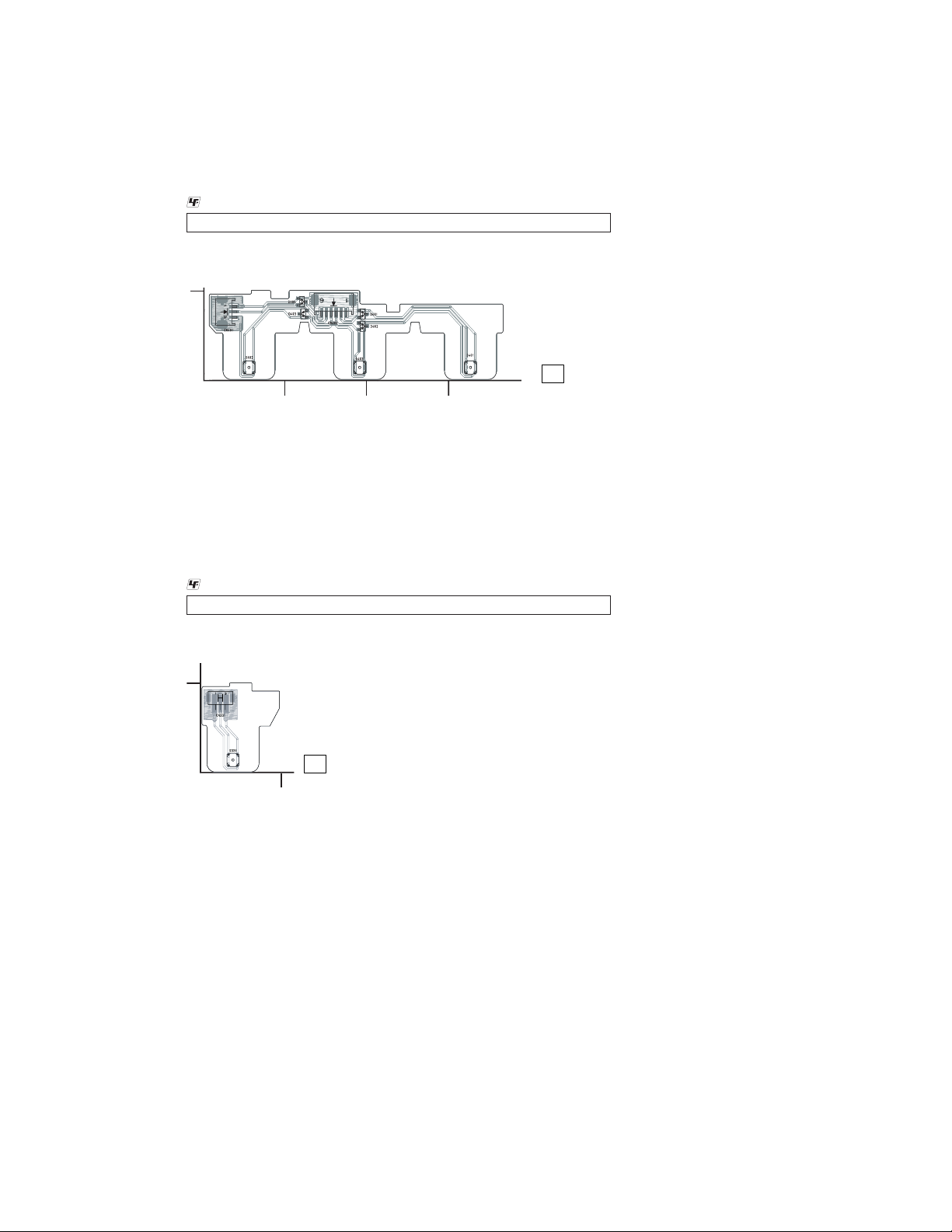
- S270/
BDP
BX37
5-2. SWB-001 (SWITCH) BOARD PRINTED WIRING BOARD
- Ref. No.: SWB-001 board; 20,000 series -
• See page 2-5 for circuit boards location.
: Uses unleaded solder.
There are a few cases that the part isn’t mounted in this model is printed on this diagram.
SWB-001
A
/S370/S373/S470
11
SWB-001 BOARD
CN401 A-1
CN402 A-2
D401 A-2
D402 A-2
D403 A-2
D404 A-2
1
2
34
1-880-458-
5-3. SWP-001 BOARD PRINTED WIRING BOARD
- Ref. No.: SWP-001 board; 20,000 series -
• See page 2-5 for circuit boards location.
: Uses unleaded solder.
There are a few cases that the part isn’t mounted in this model is printed on this diagram.
SWP-001
A
1-880-457-
11
1
SWP-001 BOARD
CN331 A-1
5-2
Page 58
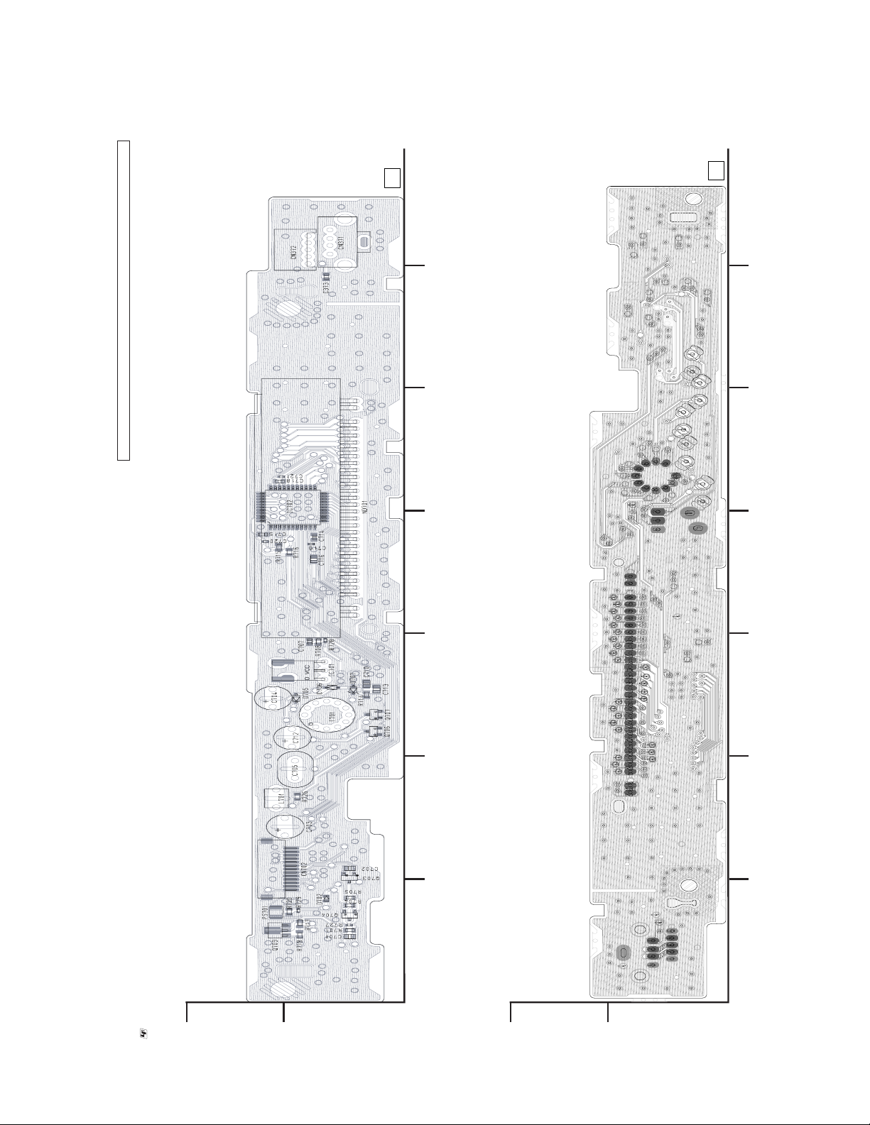
FR-309 BOARD (SIDE A)
D702 A-1
CN371 A-7
CN372 A-7
D706 A-3
D707 A-3
D705 A-3
IC701 A-3
IC702 B-5
Q703 A-1
Q704 A-1
Q706 A-3
Q707 A-3
Q709 B-1
BDP-BX37/S270/S370/S373/S470
There are a few cases that the part isn’t mounted in this model is printed on this diagram.
11
7
1-880-454-
6
FR-309
5
43
11
7
1-880-454-
6
5
5-3
43
• See page 2-5 for circuit boards location.
FR-309 BOARD (SIDE A)
: Uses unleaded solder.
5-4. FR-309 BOARD (FRONT RIGHT) PRINTED WIRING BOARD (SIDE A)
- Ref. No.: FR-309 board; 20,000 series -
B
A
2
1
2
1
FR-309 BOARD (SIDE B)
B
A
Page 59
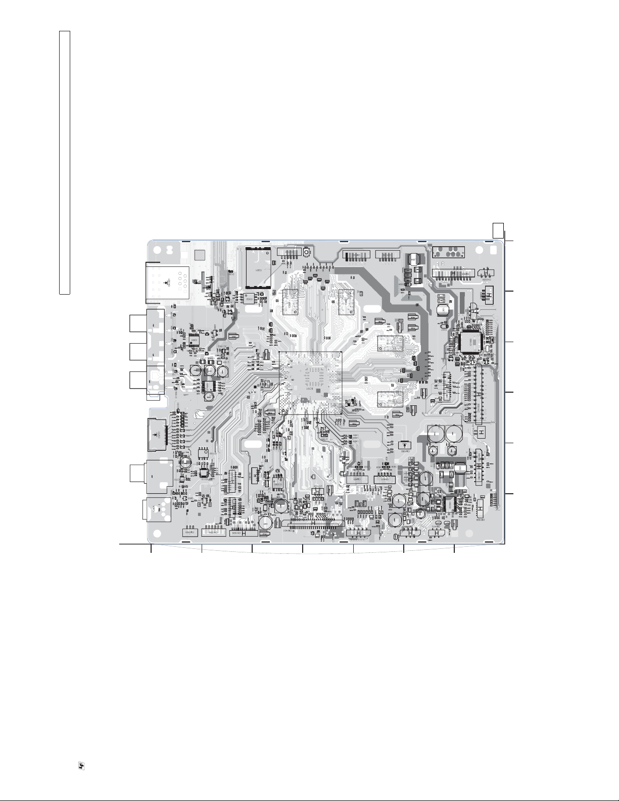
BDP-BX37/S270/S370/S373/S470
A-4
F-4
X1502 A-5
X1501 A-4
X1351 D-3
X802 D-3
X401 E-4
L2324 B-1
L1003
L2322 B-1
L1002 G-4
L1001 F-4
L704 G-3
L703 G-3
IC1451 E-1
CN1491 E-2
IC1502
CN1501 A-5
IC1503 A-4
IC1504 B-4
CN1502 C-6
CN1503 G-1
IC2301 B-1
CN1504 A-2
CN1505 A-3
L301 B-5
CN1507 A-2
CN1509 C-6
CN1506 A-1
CN1510 A-3
CN1508 A-6
IC1003 F-4
IC1101 F-2
IC1102 F-2
IC1202 F-5
IC1390 E-2
IC101 D-4
IC104 C-3
IC105 C-5
IC204 D-5
IC205 E-5
IC306 F-5
CN602 C-2
CN301 B-6
CN302 A-5
CN303 A-6
CN601 C-2
MB-134 BOARD (SIDE A)
CN701 G-3
IC1002 F-4
IC307 F-2
IC501 E-6
IC502 E-5
IC701 G-2
IC901 G-5
CN1382 B-2
CN1401 E-1
CN1201 G-6
CN1424 D-2
CN1320 F-1
CN1330 F-1
CN1102 E-6
CN904 G-1
CN901 F-1
CN902 F-2
CN1101 B-4
L304 B-6
L604 C-3
L603 C-3
L305 B-2
L303 A-2
L702 G-3
L701 G-3
L608 C-2
L607 C-2
L606 C-3
L605 C-3
D604 C-2
D603 D-2
D307 B-5
D304 C-6
D303 B-2
CN2470 B-1
CN2490 B-1
CN2460 C-1
Q1502 A-4
Q909 G-1
D1201 F-6
D1004 G-5
D1003 G-4
D1002 G-5
D1001 G-4
D906 G-2
D905 G-5
D904 G-5
D901 F-5
D701 G-3
D606 C-2
D605 C-2
CN1102
IC501
D1201
There are a few cases that the part isn’t mounted in this model is printed on this diagram.
MB-134 BOARD (SIDE A)
CN1201
IC502
IC1202
D1004
D905
IC901
D1002D904
L1002
D1001
D1003
CN701
D906
IC904
IC1003
D701
L704
L703
L702
L701
IC1101
IC701
Q909
IC307
CN1503
IC306
D901
IC1002
L1003
L1001
IC1102
CN902
CN1491
CN901
CN1330
CN1320
IC205
X401
IC1390
IC1451
CN1401
CN301
CN303
6
CN1508
1-879-998- 11
CN302
L301
CN1501
D307
IC1503
IC1504
CN1101
CN1505
CN1510
D303
L305
L2322
L2324
CN2470
CN1504
L303
CN1507
IC2301
5
X1502
X1501
Q1502
IC1502
43
5-4
2
CN1506
1
L607
CN2460
CN1509
L304
D304
IC105
IC104
CN1382
L608
D606
D604
CN602
CN2490
CN1502
IC204
IC101
X802
L605
L606
X1351
L603
L604
D603D605
CN1424
CN601
H
G
: Uses unleaded solder.
5-5. MB-134 BOARD (MAIN) PRINTED WIRING BOARD (SIDE A) • See page 2-5 for circuit boards location.
- Ref. No.: MB-134 board; 10,000 series -
F
E
D
C
B
A
Page 60
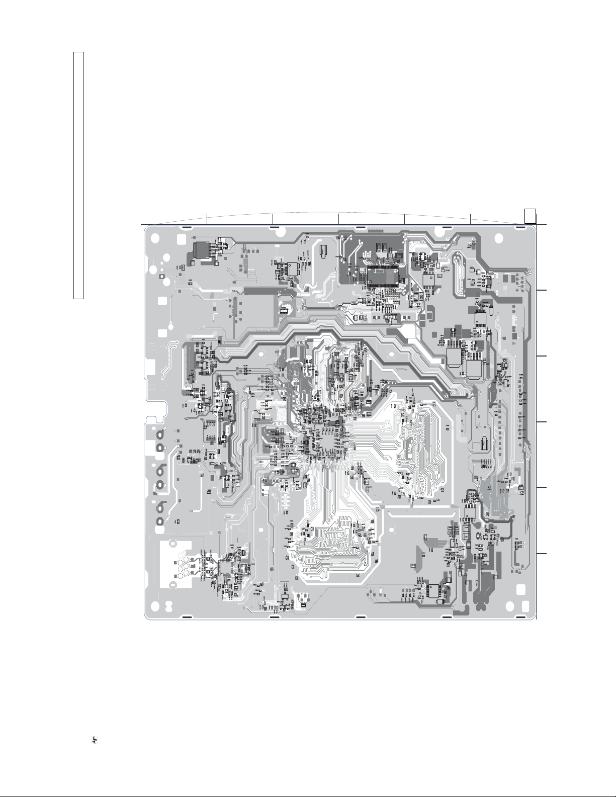
BDP-BX37/S270/S370/S373/S470
Q1501 A-1
Q502 C-6
Q503 C-6
Q701 A-3
Q702 A-3
IC305 B-4
IC308 F-5
IC309 F-2
X1201 B-6
Q1503 F-3
IC601 E-2
IC312 E-1
IC311 E-5
IC310 E-6
IC702 B-3
IC602 F-3
IC1501 A-1
IC1441 C-1
IC2480 E-2
IC1201 B-6
IC703 A-3
IC2401 D-1
IC1505 F-3
IC1001 B-4
IC705 A-2
IC704 A-3
Q302 E-1
Q303 E-1
L1202 B-6
Q301 F-5
D601 E-2
D1501 F-3
D602 F-2
Q501 C-6
IC302 F-5
IC301 F-6
IC303 B-3
IC304 A-4
L306 E-6
L1201 B-6
L302 E-5
D305 F-2
D302 F-5
D306 E-6
MB-134 BOARD (SIDE B)
A
IC1501
B
Q1501
IC1441
There are a few cases that the part isn’t mounted in this model is printed on this diagram.
IC705
Q702
IC704
K2
Q701
IC303
IC703
• See page 2-5 for circuit boards location.
IC304
IC702
IC305
IC1001
IC2480
E
Q302
Q303
IC312
IC309
D601
IC601
IC602
C
D
IC2401
F
11
1
1-879-998-
D305
23456
D602
IC1505
D1501
Q1503
5-5
L1202
IC1201
L1201
X1201
Q503
Q501
MB-134 BOARD (SIDE B)
: Uses unleaded solder.
5-6. MB-134 BOARD (MAIN) PRINTED WIRING BOARD (SIDE B)
- Ref. No.: MB-134 board; 10,000 series -
Q502
IC308
D302
IC302
IC311
L306
IC310
D306
Q301
L302
IC301
PS302
PS304
PS303
PS301
05
Page 61
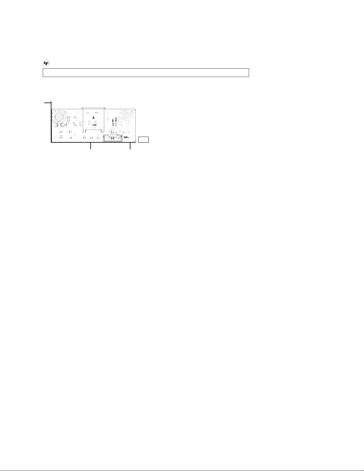
6E
There are a few cases that the part isn’t mounted in this model is printed on this diagram.
: Uses unleaded solder.
- Ref. No.: USB-023 board; 20,000 series -
• See page 2-5 for circuit boards location
.
CN361 A-2
CN362 A-2
A
USB-023
1
2
1-880-456
11
-
Page 62

BDP-BX37/S270/S370/S373/S470
SECTION 6
IC PIN FUNCTION DESCRIPTION
MAIN SYSTEM CONTROL PIN FUNCTION (MB-134 BOARD IC101: CXD9983GG/CXD9984GG)
Pin Symbol Type Description
A1 FESFDO I/O
A3 VOUTD1 I/O
A5 VOUTD5 I/O
A7 VOUTD9 I/O
A9 VOUTD12 I/O
A11 VIND0 I/O
A13 VIND12 I/O
A15 VIND16 I/O
A17 GPIO1 I/O
A19 SPDIF I/O
A21 SPBCK I/O SPDIF in Bit Clock
A23 AVDD12_27 MPLL Power 1.2V Analog Power for PLL
A25 NS_XTALI O 27MHz Crystal Out
A27 CH1_M Analog HDMI TX data 1 differential pair (M)
A29 CLK_M Analog HDMI TX clock differential pair (M)
A31 DACOUT4 Analog DAC Output
A33 DACOUT1 Analog DAC Output
A35 VCLK I/O VFD Clock (IF_SCK)
A37 UARXD I/O
A39 ETRXD3 I/O
A41 ETRXD0 I/O
A43 ETRXCLK I/O
B2 FESFCS I/O
B4 VOUTD3 I/O NC
B6 VOUTD7 I/O NC
B8 VOUTD10 I/O
B10 VOUTD14 I/O
B12 VIND4
B14 VIND14 I/O
B16 VINHSYNC I/O NC
B18 GPIO3
B20 SPLRCK I/O SPDIF in Left-Right Clock
B22 AOBCK I/O Audio Out Bit Clock
B24 AVDD12_DMPLL Power 1.2V Analog Power for DMPLL
B26 CH2_M Analog HDMI TX data 2 differential pair (M)
B28 CH0_M Analog HDMI TX data 0 differential pair (M)
B30 EXT_CAP Analog NC
B32 DACOUT3 Analog DAC Output
B34 VDATA I/O
B38 ETMDIO I/O
B40 ETRXD1 I/O
B42 ETRXER I/O
I/O
I/O
O/IRI63B
Serial Data Input to Front_End Serial Flash
NC
NC
NC
NC
NC
NC
NC
GPIO
START-BIT
SPDIF Digital Audio Out
RS232 RX
CPU_UARXD
Receive Data from the PHY
Receive Data from the PHY
Receive Clock from the PHY
Front-END Serial Flash Chip Select
NC
NC
GPIO
DAC_XRST
NC
GPIO
USB_VBUS_PCONT2
VFD Data (IF_SDO)
Infrared Input
Management Data INPUT/OUTPUT from/to the MDIO pin
Receive Data from the PHY
Receive Error Signal from the PHY
FE_SFCLKC1
C3 FESFDI I
C5 VOUTD4 I/O
C7 VOUTD8 I/O
C9 VOUTD11 I/O
C11 VOUTD15 I/O
C13 VIND11 I/O
C15 VIND15 I/O
GPIO0 I/O
C17
GPIO2C19
C21 SPMCLK I/O SPDIF in Master Clock
C23 AOSDATA0 I/O Audio Out Serial Data 0
C27 CH1_P Analog HDMI TX data 1 differential pair (P)
C29 CLK_P Analog HDMI TX clock differential pair (P)
C31 DACOUT5 Analog DAC Output
C33 DACOUT2 Analog DAC Output
C35 MRESET_ O Front-End Power ON Reset
C37 ETCO
C39 ETRXD2 I/O
C41
C43 ETTXD0 I/O
D4
D6 VOUTD6 I/O
D8 VOUTD0 I/O
D10 VOUTD13 I/O
D12 VIND1 I/O
D14 VIND13 I/O
D16 VINCLK I/O
D18 VIND17 I/O
D20 AOSDATA5 I/O Audio Out Serial Data 5
L I/O
ETTXCLK I/O
FE_GIO11D2
FESFCK I/O
I/O
I/O
3.3V LVTTL I/O,
Serial Flash's Clock OUTPUT
NC
Serial Data Output to Front-END Serial Flash
NC
NC
NC
NC
NC
NC
GPIO
SYSCON_REQ
GPIO
XIF_CS
nI latsyrC zHM72IOLATX_SN52C
Collision Detect From the PHY
Receive Data from the PHY
Transmit Clock from the PHY
Transmit Data from the PHY
UTXD.
FE RS232 Serial Transmit data.
NC
Front-END Serial Flash Clock
NC
NC
NC
NC
NC
NC
NC
6-1
Page 63
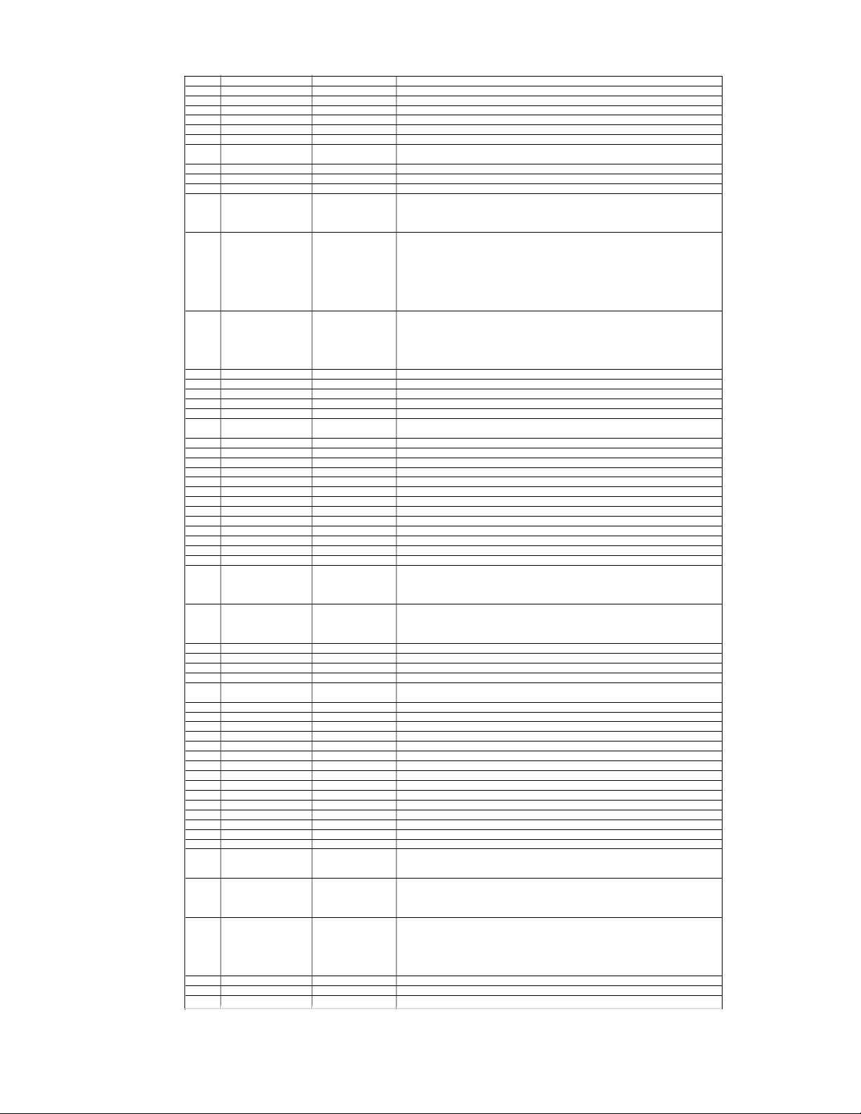
D22 AOMCLK I/O Audio Out Master Clock
G15
VIND8
I/O
D24 AVDD12_APLL Power 1.2V Analog Power for APLL
D26 CH2_P Analog HDMI TX data 2 differential pair (P)
D28 CH0_P Analog HDMI TX data 0 differential pair (P)
D30 DACOUT6 Analog DAC Output
D32 AVDD33_VDACBG Power 3.3V Analog Power
D34 VSTB I/O
D36 UATXD
D38 ETTXEN I/O
D40 ETTXD1 I/O
D42 ETTXD2 I/O
E1 FE_SFDO
I/O
I/O
NC
RS232 TX
CPU_UATXD
Transmit Enable to the PHY
Transmit Data from the PHY
Transmit Data from the PHY
Serial Data OUTPUT
NC
BDP-BX37/S270/S370/S373/S470
E3 FE_GIO2
E5 FE_GIO9
E7 VOUTD2 I/O
E9
VOUTCLK1 I/O NC
E11 VOUTD16 I/O
E13 VOUTD19 I/O
E15 VIND2 I/O
VINVSYNC
E17
E19 VIND19 I/O
E21 AOSDATA4 I/O Audio Out Serial Data 4
E23
AOLRCK I/O
E25 AVDD33_XTAL Power 3.3V Analog Power for XTAL
E27 TN_PLLG Analog Test Pin
E29 EXT_RES Analog HDMI reference voltage
E31 AVDD33_VDACR Power 3.3V Analog Power
E33 DACFS Analog DAC Full Scale
E37 ETTXER I/O
E39 ETTXD3 I/O
E41 HDMISD I/O
E43 CEC I/O
F2 FE_SFD1
F6 NS_CKIN33 Analog SACD Clock INPUT
F8 VOUTCLK2 I/O
F10 VOUTHSYNC I/O NC
F12 VOUTD17 I/O
F14 VIND5 I/O
F16 VIND3 I/O
F18 VIND7 I/O
F20 MCIN I/O Microphone In/Line In
F22 AOSDATA3 I/O Audio Out Serial Data 3
F24
AVSS12_DMPLL Ground Analog Ground for DMPLL
F26 TN_PLLG Analog Test Pin
F28 AVSS33_HDMI Ground Analog Ground
F30 AVDD12_HDMI Power 1.2V Analog Power
F32 AVSS33_VDACBG Ground Analog Ground
F34 OPWRSB I/O Power Control
F36 ETMDC I/O
F38 ETRXDV I/O
F40 HDMISCK I/O
F42 SFDO I/O Data OUTPUT to Serial Flash
G1 FE_VRDC0 Analog Output
FE_FGG3
I/O
I/O
I/O
I/O
I/O
I/O
General IO.
NC
SACD CLOCK
NC
NC
NC
NC
GPIO
ETHER_XRST
NC
Audio Out Left-Right Clock
Transmit Error Signal to the PHY
Transmit Data from the PHY
HDMI I2C Data
HDMI CEC
Serial Data INPUT
NC
NC
NC
NC
GPIO
USB_VBUS_PCONT1
NC
NC
Management Data Clock to the PHY
Receive Data valid signal from the PHY
HDMI I2C Clock
NC
Spindle FG input
teseR NO rewoPI_TESER53E
edoM hsalF laireS lamron ni dloH#DLOHFS_EF4F
FE_GIO7
G5
G9
FE_GIO6
G11 VOUTVSYNC I/O
G13 VOUTD18 I/O
I/O
Analog Output
LDEN
BU Laser diode control
MODE_C
OEIC Mode SW
NC
NC
GPIO
6-2
Page 64
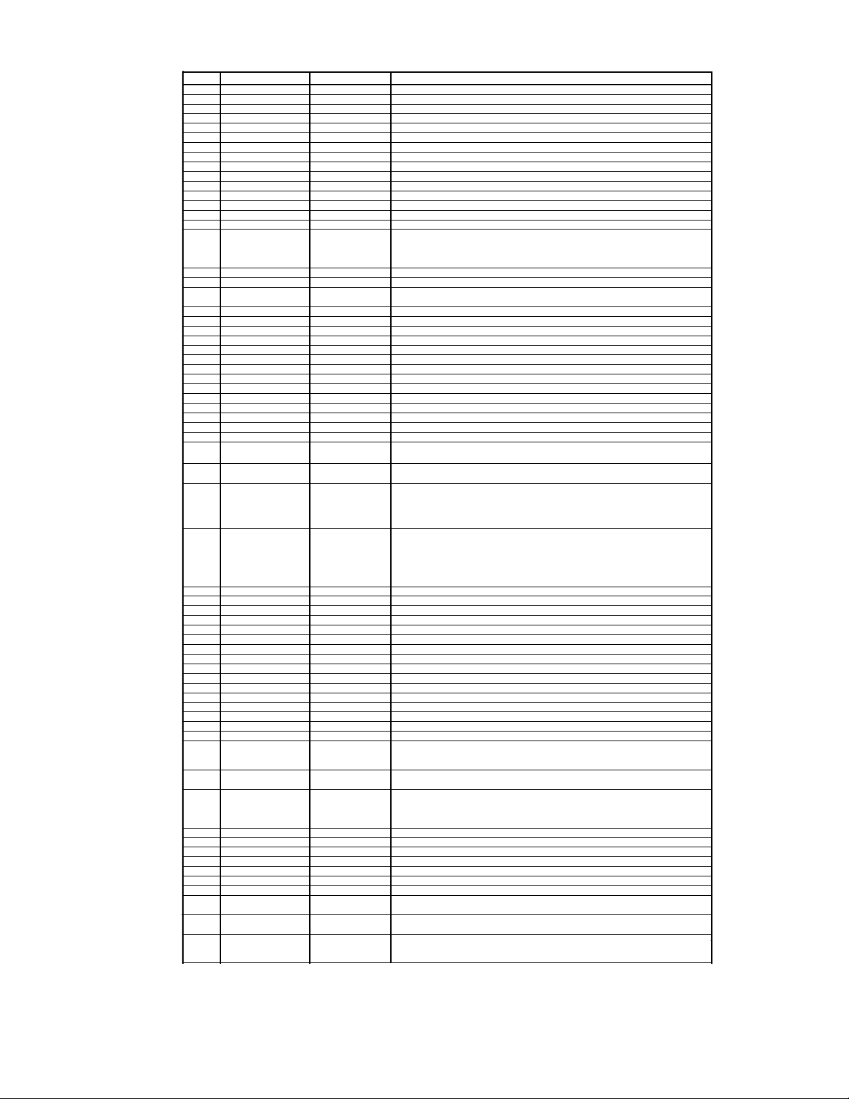
G15
T
VIND8
G17 VIND10 I/O
G19 VIND18 I/O
G21 SPDATA I/O SPDIF in Serial Dat
G23 AOSDATA1 I/O Audio Out Serial Data 1
G25 AVSS33_XTAL Ground Analog Ground for XTAL
G27 AVSS33_HDMI Ground Analog Ground
G29 AVDD12_HDMI Power 1.2V Analog Power
G31 AVDD33_VDACY Power 3.3V Analog Power
G33 LCDRD I/O
G35 VCC3IO_ST B Power 3.3V Digital IO Power for Stand-By Module
G37 DVSS Ground Digital Ground
G39 HTPLG I/O
G41 SFCK I/O
G43 NFWEN I/O
H4 NS_RFIN Analog SACD Input
FE_GIO10
H8
H10 VCC3IO_3 Power 3.3V Digital IO Power
H12 VCC3IO_3 Power 3.3V Digital IO Power
H14 VIND6
H16 DVSS Ground Digital Ground
H18 VCC3IO_3 Power 3.3V Digital IO Power
H20 AMUTE I/O Audio DAC Mute (XAMUTE)
H22 AOSDATA2 I/O
H24 AVSS12_APLL Ground Analog Ground for APLL
H26 AVDD33_HDMI Power 3.3V Analog Power
H28 AVSS12_HDMI Power Analog Ground
H30 AVSS33_VDACY Ground Analog Ground
H32 AVSS33_VDACR Ground Analog Ground
H34 ETCRS I/O
H36 DVSS Ground Digital Ground
H38 AVDD10_LDO Power 1.0V Standby Power
H40 SFDI I/O
H42 NFD0 I/O
J1 FE_HAVC Analog Output
J3 FE_MPXOUT3 Analog Output
FE_GIO5 Analog OutputJ5
I/O
I/O
I/O
FORMAT1
NC
NC
Serial Interface Master Data Line (IF_SDI)
HDMI Hot Plug
Serial Flash Clock
NAND Flash Write Enable
URXD (FE RS232 Serial Receive data)
NC
GPIO
XVMUTE
Audio Out Serial Data 2
Carrier Sense From the PHY
Data INPUT from Serial Flash
NAND Flash Data INPUT/OUTPUT bit0
VC_PD
Reference Voltage of Main and Sub Beams
Multiplexer Output 3 for Signal Monitoring
NC
MODE_B
OEIC Select SW
BDP-BX37/S270/S370/S373/S470
J7 FE_GIO4
J9 DVSS Ground Digital Ground
J11 DVSS Ground Digital Ground
J13 DVSS Ground Digital Ground
J15 VCC3IO_3 Power 3.3V Digital IO Power
J17 VIND9 I/O
J19 DVSS Ground Digital Ground
J21 VCC3IO_P WM Power 3.3V DIgital IO Power for PWM
J23 DVSS Ground Digital Ground
J25 AVSS12_27MPLL Ground Analog Ground for PLL
J27 AVDD33_HDMI Power 3.3V Analog Power
J29 AVSS12_HDMI Power Analog Ground
J33 VCC3IO_ST B Power 3.3V Digital IO Power for Stand-By Module
J37 AVDD33_LDO Power 3.3V Power
J39 SFCS I/O
J41 NFD1 I/O
J43 NFD2 I/O
K2 FE_MPXOUT2
K4 FE_EQBIAS Analog Output
K8 NS_RFIP Analog SACD Input
K34 DVSS Ground Digital Ground
K36 AVSS33_LDO Ground Analog Ground
K38 NFCLE I/O
K40 NFD3 I/O
K42 NFD4 I/O
L1 FE_VWDC3O Analog Outpu
L3 FE_VDAC0 Analog Output
L5
FE_SFWP#
L7
Analog Output
Analog Output
I/O
Analog OutputFE_MPXOUT1
I/O
MODE_A
OEIC Gain SW
NC
Serial Flash Chip Select
NAND Flash Data INPUT/OUTPUT bit1
NAND Flash Data INPUT/OUTPUT bit2
Multiplexer Output 2 for Signal Monitoring.
NC
External Bias Connection for Circuits in EQRF Block & SATA Block. The external resistor
need meet the precision for SATA requirement. (23.1K,1%)
NC
NAND Flash Command Latch Enable
NAND Flash Data INPUT/OUTPUT bit3
NAND Flash Data INPUT/OUTPUT bit4
NC
t
SA_INT
SA Initialize
Multiplexer Output 1 for Signal Monitoring.
NC
Serial Flash Write Protect
NC
TUPNI tceleS pihC#SCFS_EF6K
6-3
Page 65

BDP-BX37/S270/S370/S373/S470
L9 FE_GIO8
L35 VCC3IO_1 Power 3.3V Digital IO Power
L37 NFALE I/O
L39 NFCEN2 I/O
L41 NFD5 I/O
L43 NFD6 I/O
M2 FE_VWDC2O Analog Output
M4 FE_AUX1 Analog I/O
M6 FE_RSTI Analog Input Intenal power ON Reset detection input
M8 FE_MVDDQ DRAM Power (3.3V) VDD for pad output buffer of DRAM die
M10 FE_MVDDQ DRAM Power (3.3V) VDD for pad output buffer of DRAM die
M36 NFREN I/O
M38 NFCEN I/O
M40 NFD7 I/O
N1 FE_INB Analog Input Input of Main Beam Signal (B)
N3 FE_TRINC Analog Input
N5 FE_VFVREF Analog Output Output of Voltage Reference
N7
FE_DVDD33O Digital Power (3.3V) VDD for Digital Pad
N9
FE_DVDD33O Digital Power (3.3V) VDD for Digital Pad
N11
FE_DVDD33O Digital Power (3.3V) VDD for Digital Pad
N35 VCC3IO_1 Power 3.3V Digital IO Power
N37 DVSS Ground Digital Ground
N39 DVSS Ground Digital Ground
N41 B_RCLK1 O Memory Clock 1 Positive
N43 B_RCLK1_ O Memory Clock 1 Negative
P2 FE_INA Analog Input Input of Main Beam Signal (A)
P4 FE_TRINA Analog Input
P6 FE_VWDC2O Analog Output
P8 FE_AVDD12_1 Analog Power (1.2V) Power pin
P10
FE_DVDD33O Digital Power (3.3V) VDD for Digital Pad
P12
DVSS Ground Digital Ground
P14
DVSS Ground Digital Ground
P36 NFRBN2 I/O
P38 NFRBN I/O
P40 VCC2IO Power 1.8V Digital IO Power
P42 VCC2IO Power 1.8V Digital IO Power
R1 FE_ING Analog Input Input of Sub-Beam Signal (G)
R3 FE_INC Analog Input Input of Main Beam Signal (C)
R5 FE_TRINB Analog Input
R7 FE_TRIND Analog Input
R9 FE_AVDD12_2 Analog Power (1.2V) Power pin
R35
DVSS Ground Digital Ground
R37 B_RDQ25 I/O Memory Data bit 25
R39 B_RDQ30 I/O Memory Data bit 30
R41 B_RDQ29 I/O Memory Data bit 29
R43 B_RDQ26 I/O Memory Data bit 26
T2 FE_INH Analog Input Input of Sub-Beam Signal (H)
T4 FE_FPDODVD Analog Input Laser Power Monitor Input for DVD APC
T6 FE_IND Analog Input Input of Main Beam Signal (D)
T8 FE_DVDD12I Digital Power (1.2V) VDD for Internal Circuit
T10 FE_DVDD12I Digital Power (1.2V) VDD for Internal Circuit
T12
DVSS Ground Digital Ground
T14
DVSS Ground Digital Ground
T36 B_RDQ28 I/O Memory Data bit 28
B_RDQ27 I/O Memory Data bit 27
T38
T40 B_RDQ24 I/O Memory Data bit 24
T42 B_RDQ31
FE_INF Analog Input Input of Sub-Beam Signal (F)
U1
U3 FE_FOIN
U5 FE_FPDOCD Analog Input
U7 FE_V14 Analog Output Output of Voltage Reference (1.4V)
U9 FE_AVDD33 Analog Power (3.3V) Power pin
U11 FE_DVDD12I Digital Power (1.2V) VDD for Internal Circuit
U13
DVSS Ground Digital Ground
U15
DVSS Ground Digital Ground
U35
DVSS Ground Digital Ground
U37
DVSS Ground Digital Ground
U39
DVSS Ground Digital Ground
U41 B_RDQS3_ I/O Memory Negative Data Strobe bit 3
U43 B_RDQS3_ I/O Memory Positive Data Strobe bit 3
V2 FE_FOIP
V4 FE_REG_CAP Analog Output Output of Voltage Reference
V6 FE_INE Analog Input Input of Sub-Beam Signal (E)
V8 FE_AVDD33 Analog Power (3.3V) Power pin
V10 FE_DVDD12I Digital Power (1.2V) VDD for Internal Circuit
V12
DVSS Ground Digital Ground
V14
DVSS Ground Digital Ground
V36 B_RDQM3 O Memory Data Mask bit 3
V38 B_RDQM2 O Memory Data Mask bit 2
V40 VCC2IO Power 1.8V Digital IO Power
V42 VCC2IO Power 1.8V Digital IO Power
W1 FE_RFIP2 Analog Input Differential Input of AC Coupling DVD RF SUM Signal (Positive)
W3 FE_RFIN2 Analog Input Differential Input of AC Coupling DVD RF SUM Signal (Negative)
W5 FE_AGND Analog Ground Analog Ground
W7 FE_AGND Analog Ground Analog Ground
W9 FE_AVDD33 Analog Power (3.3V) Power pin
W11 FE_DVDD12I Digital Power (1.2V) VDD for Internal Circuit
W13
DVSS Ground Digital Ground
W15
DVSS Ground Digital Ground
I/O GIO8
I/O Memory Data bit 31
Analog Input
Analog Input
NC
NAND Flash address Latch Enable
NAND Flash 2nd Chip Enable
NAND Flash Data INPUT/OUTPUT bit5
NAND Flash Data INPUT/OUTPUT bit6
NC
Thermo- BU Temperature Monitor
NAND Flash Read Enable
NAND Flash Chip Enable
NAND Flash Data INPUT/OUTPUT bit7
NC
NC
NC
NC
NAND Flash ready/busy
NC
NC
NC
NC
NC
noitarbilaC revirD pihC-nOINDTXER_B24M
6-4
Page 66

BDP-BX37/S270/S370/S373/S470
W21 VCCK Power 1.1V Digital Power
W23 VCCK Power 1.1V Digital Power
W25 VCCK Power 1.1V Digital Power
W27 VCCK_PWM Power 1.1V Digital Power for PWM
W29 VCCK Power 1.1V Digital Power
W31 VCCK Power 1.1V Digital Power
W35 VCC2IO Power 1.8V Digital IO Power
W37 B_RDQ18 I/O Memory Data bit 18
W39 B_RDQ21 I/O Memory Data bit 21
W41 B_RDQS2 I/O Memory Positive Data Strobe bit 2
W43 B_RDQS2_ I/O Memory Negative Data Strobe bit 2
Y2 FE_RFIP Analog Input Differential Input of AC Coupling BD RF SUM Signal (Positive)
Y4 FE_RFIN Analog Input Differential Input of AC Coupling BD RF SUM Signal (Negative)
Y6
FE_LVDS_1N Analog Output LVDS 1N
Y8 FE_AGND Analog Ground Analog Ground
Y10 FE_DVDD12I Digital Power (1.2V) VDD for Internal Circuit
Y14
DVSS Ground Digital Ground
Y20 VCCK Power 1.1V Digital Power
Y22
DVSS Ground Digital Ground
Y24
DVSS Ground Digital Ground
Y26
DVSS Ground Digital Ground
Y28
DVSS Ground Digital Ground
Y30
DVSS Ground Digital Ground
Y32 VCCK Power 1.1V Digital Power
Y36 B_RDQ23 I/O Memory Data bit 23
Y38 B_RDQ16 I/O Memory Data bit 16
Y40 B_RDQ20 I/O Memory Data bit 20
Y42 B_RDQ22 I/O Memory Data bit 22
AA1
FE_LVDS_2P Analog Output
AA3
FE_LVDS_2N Analog Output
AA5
FE_LVDS_1P Analog Output
AA7 FE_AGND Analog Ground Analog Ground
AA9 FE_AVDD33_lvds Analog Power (3.3V) Power pin
AA21
DVSS Ground Digital Ground
AA23 VCCK Power 1.1V Digital Power
AA25 VCCK Power 1.1V Digital Power
AA27 VCCK Power 1.1V Digital Power
AA29 VCCK Power 1.1V Digital Power
AA31
DVSS Ground Digital Ground
AA35
DVSS Ground Digital Ground
AA37
DVSS Ground Digital Ground
AA39
DVSS Ground Digital Ground
AA41 B_RDQ17 I/O Memory Data bit 17
AA43 B_RDQ19 I/O Memory Data bit 19
AB2
FE_LVDS_4N Analog Output
AB4
FE_LVDS_3N Analog Output
AB6
FE_LVDS_5N
AB8 FE_AVDD12_3 Analog Power (1.2V) Power pin
AB10
FE_DVDD33O Digital Power (3.3V) VDD for Digital Pad
AB12
FE_DVDD33O Digital Power (3.3V) VDD for Digital Pad
AB20 VCCK Power 1.1V Digital Power
AB22 VCCK Power 1.1V Digital Power
AB24
DVSS Ground Digital Ground
AB26
DVSS Ground Digital Ground
AB28
DVSS Ground Digital Ground
AB30 VCCK Power 1.1V Digital Power
AB32 VCCK Power 1.1V Digital Power
AB40 VCC2IO Powe
AB42 VCC2IO Power 1.8V Digital IO Power
AC1
FE_LVDS_4P Analog Output
AC3
FE_LVDS_3P Analog Output
AC5
FE_LVDS_5P
AC7 FE_AVDD12_4 Analog Power (1.2V) Power pin
AC9
FE_DVDD33O Digital Power (3.3V) VDD for Digital Pad
AC21
DVSS Ground Digital Ground
AC23
DVSS Ground Digital Ground
AC25
DVSS Ground Digital Ground
AC27
DVSS Ground Digital Ground
AC29
DVSS Ground Digital Ground
AC31
DVSS Ground Digital Ground
AC37 B_RA5 O Memory Address bit 5
AC39 B_RBA2 O Memory Bank Address bit 2
AC41 B_RCKE O Memory Clock Enable
AC43 B_RWE_ O Memory Write Enable
AD2 FE_CFREQ
Analog Output
r 1.8V Digital IO Power
Analog Output
I/O,
NC
NC
NC
NC
NC
NC
FERV yromeMIFERVR_B63BA
NC
NC
NC
FE_LDD_SDIO
LDD Serial Interface Data
AD4 FE_FOO Analog Output Focus servo OUTPUT.
AD6 FE_GAINSW2 Analog Output
AD8 FE_GIO0
AD20 VCCK Power 1.1V Digital Power
AD22 VCCK Power 1.1V Digital Power
AD24
DVSS Ground Digital Ground
AD26
DVSS Ground Digital Ground
I/O,
Motor Driver Gain switch
MUTE1
Motor Driver Mute Control
6-5
Page 67
AD28
DVSS Ground Digital Ground
AD30 VCCK Power 1.1V Digital Power
AD32 VCCK Power 1.1V Digital Power
AD36 B_RBA1 O Memory Bank Address bit 1
AD38 B_RA9 O Memory Address bit 9
AD40 B_RBA0 O Memory Bank Address bit 0
AD42 B_RCS_ O Memory Chip Select
AE1 FE_FMO Analog Output Feed motor control. PWM Output
AE3 FE_TRAYPWM Analog Output Tray PWM control OUTPUT. Controlled by μP
AE5
FE_GAINSW1
Analog Output
STEP_ENA
SA motor step enable control
BDP-BX37/S270/S370/S373/S470
AE7 FE_OSCEN
AE9 FE_GIO12
AE21
DVSS Ground Digital Ground
AE23
DVSS Ground Digital Ground
AE25
DVSS Ground Digital Ground
AE27
DVSS Ground Digital Ground
AE29
DVSS Ground Digital Ground
AE31
DVSS Ground Digital Ground
AE35
DVSS Ground Digital Ground
AE37
DVSS Ground Digital Ground
AE39
DVSS Ground Digital Ground
AE41
B_RA12 O Memory Address bit 12
AE43
B_RA7 O Memory Address bit 7
AF2 FE_DMO Analog Output Disk motor control Output. PWM Output
AF4 FE_FMO2 Analog Output Feed motor 2 control. PWM Output
FE_FMO4
AF6
AF8 FE_CMOD
AF20 VCCK Power 1.1V Digital Power
AF22 VCCK Power 1.1V Digital Power
AF24 DVSS Ground Digital Ground
AF26 DVSS Ground Digital Ground
AF28 DVSS Ground Digital Ground
AF30 VCCK Power 1.1V Digital Power
AF32 VCCK Power 1.1V Digital Power
AF36 B_RA11 O Memory Address bit 10
AF38 B_RA2 O Memory Address bit 2
AG1 FE_GIO3
AG3 FE_LIMIT
I/O,
I/O,
Analog I/O
I/O,
I/O,
I/O,
LDD_SCLK
LDD Serial Interface CLK
GIO12
NC
SA_B
SA motor control output
LDD_SEN
LDD Serial Interface command Enable.
LED 1
LED Control Output
NC
Sled Inner Limit Input
FE_GAINSW3
AG9 FE_GIO1
AG21 DVSS Ground Digital Ground
AG23 DVSS Ground Digital Ground
AG25 DVSS Ground Digital Ground
AG27 DVSS Ground Digital Ground
AG29 DVSS Ground Digital Ground
AG31 DVSS Ground Digital Ground
AG37 B_RA2 O Memory Address bit 2
AG39 B_RA6 O Memory Address bit 6
AG41 B_RODT O Memory On Die Terminal Enable
AG43 B_RA0 O Memory Address bit 0
AH2 FE_PLAY#
FE_EJECT#AH4
AH6 FE_TRO
AH20 VCCK Power 1.1V Digital Power
AH22 VCCK Power 1.1V Digital Power
AH24 DVSS Ground Digital Ground
AH26 DVSS Ground Digital Ground
AH28 DVSS Ground Digital Ground
AH30 VCCK Power 1.1V Digital Power
AH32 VCCK Power 1.1V Digital Power
AH36 B_RA8 O Memory Address bit 8
AH38 B_RA11 O Memory Address bit 11
Analog OutputAG5
Analog I/OFE_FMO3AG7
I/O,
I/O,
I/O,
Analog Output
NC
SA_A
SA motor control input
MUTE1
Motor Driver Mute Control
NC,
FE_Eject
FE_Eject Control
Tracking Servo OUTPUT
6-6
Page 68
AH40 B_RCAS_ O Memory Column Address Strobe
AH42 B_RA4 O Memory Address bit 4
AJ1 FE_XTAL25MO Output X'tal Output
AJ3 FE_XTAL25MI Input X'tal Input. The working frequency is 25Mhz
AJ5 FE_TRAYIN#
AJ7 DVSS_xtal Digital Ground Digital Ground
AJ9 VCLK25MI O 25MHz Clock
AJ21 DVSS Ground Digital Ground
AJ23 VCCK Power 1.1V Digital Power
AJ25 VCCK Power 1.1V Digital Power
AJ27 VCCK Power 1.1V Digital Power
AJ29 VCCK Power 1.1V Digital Power
AJ31 DVSS Ground Digital Ground
AJ35 DVSS Ground Digital Ground
AJ37 DVSS Ground Digital Ground
AJ39 DVSS Ground Digital Ground
AJ41 B_RRAS_ O Memory Row Address Strobe
AJ43 B_RA3 O Memory Address bit 3
AK2 USB_DM0 Analog USB Port1 Differential Serial Data Bus (minus)
AK4 FE_TRAYOUT
AK6 AVSS12_USB Ground Analog Ground for USB
AK8 AVSS12_USB Power 1.2V Analog Power for USB
AK20 VCCK Power 1.1V Digital Power
AK22 DVSS Ground Digital Ground
AK24 DVSS Ground Digital Ground
AK26 DVSS Ground Digital Ground
AK28 DVSS Ground Digital Ground
AK30 DVSS Ground Digital Ground
AK32 VCCK Power 1.1V Digital Power
AK36 B_RDQ9 I/O Memory Data bit 9
AK38 B_RA13 O Memory Address bit 13
AK40 VCC2IO Power 1.8V Digital IO Power
AK42 VCC2IO Power 1.8V Digital IO Power
AL1 USB_DP0 Analog USB Port1 Differential Serial Data Bus (plus)
AL3 USB_DM1 Analog USB Port2 Differential Serial Data Bus (minus)
AL5 AVSS33_USB Ground Analog Ground for USB
AL7 FE_SVDD33 Analog Power (3.3V) Power Supply for SATA 3.3V Circuitry
AL21 VCCK Power 1.1V Digital Power
AL23 VCCK Power 1.1V Digital Power
AL25 VCCK Power 1.1V Digital Power
AL27 VCCK Power 1.1V Digital Power
AL29 VCCK Power 1.1V Digital Power
AL31 VCCK Power 1.1V Digital Power
AL35 VCC2IO Power 1.8V Digital IO Power
AL37 B_RDQ11 I/O Memory Data bit 11
AL39 B_RDQ14 I/O Memory Data bit 11
AL41 B_RCLK0_ O Memory Clock 0 Negative
AL43 B_RCLK0 O Memory Clock 0 Positive
AM2 USB_DP1 Analog USB Port2 Differential Serial Data Bus (plus)
AM4 USB_VRT Analog USB Reference Resistor
AM6 FE_SXDD33 Analog Power (3.3V) SXVDD33
AM8 FE_TLO Analog Output Tilt Servo OUTPUT
AM36 B_RDQM1 O Memory Data Mask bit 1
AM38 B_RDQ12 I/O Memory Data bit 12
AM40 B_RDQ10 I/O Memory Data bit 10
AM42 B_RDQ13 I/O Memory Data bit 13
AN1 FE_STPXP Analog Output Differential Serial OUTPUT Transmit signal of SATA
AN3 AVSS33_USB Power 3.3V Analog Power for USB
AN5 FE_SAGND Analog Ground Ground Pin for SATA circuitry
AN7 FE_SPLLVDD12 Analog Power (1.2V) Power Supply for SATA Circuitry
AN35 DVSS Ground Digital Ground
AN37 DVSS Ground Digital Ground
AN39 DVSS Ground Digital Ground
AN41 B_RDQ15 I/O Memory Data bit 15
AN43 B_RDQ8 I/O Memory Data bit 8
AP2 FE_STXN Analog Output Differential Serial OUTPUT Transmit signal of SATA
AP6 FE_STXVDD12 Analog Power (1.2V) Power Supply for SATA Transmit Circuitry
AP8 FE_AVDD12_RX Analog Power (1.2V) Power Supply for SATA Circuitry
AP36 B_RDQ7 I/O Memory Data bit 7
AP38 B_RDQM0 O Memory Data Mask bit 0
AP40 VCC2IO Power 1.8V Digital IO Power
AP42 VCC2IO Power 1.8V Digital IO Power
AR1 FE_SRXN Analog Input Differential INPUT Receive signal of SATA
AR3 FE_SRXP Analog Input Differential INPUT Receive signal of SATA
AR5 RTCRBIAS Analog RTC External Resistor
AR7 AVDD12_ADC Power 1.2V Analog Power for SACD
AR17 DVSS Ground Digital Ground
AR19 VCC2IO Power 1.8V Digital IO Power
AR25 DVSS Ground Digital Ground
AR29 DVSS Ground Digital Ground
AR31 VCC2IO Power 1.8V Digital IO Power
AR37 B_RDQ6 I/O Memory Data bit 6
AR39 B_RDQ0 I/O Memory Data Bit 0
AR41 B_RDQS1_ I/O Memory Negative Data Strobe bit 1
AR43 B_RDQS1 I/O Memory Positive Data Strobe bit 1
I/O,
I/O,
Tray_is_in Input, A logical low Indicates the Tray is IN. Feedback Flag is from Tray
Connector.
Tray_is_out Input, A logical low Indicates the Tray is OUT. Feedback Flag is from Tray
Connector.
teseR nO rewoPIBTESER_EROC4PA
NI latsyrC
K867.23ICTR_IX2TA
BDP-BX37/S270/S370/S373/S470
6-7
Page 69

AT4 XO_RTC O 32.768K Crystal OUT
AT6 AVSS12_ADC Ground Analog Ground for SACD
BDP-BX37/S270/S370/S373/S470
FE_GIO13AT10
AT12 SCL I/O Slave I2C Clock
AT14 DVSS Ground Digital Ground
AT16
A_RDQ5 I/O Memory Data bit 5
AT18
A_RDQM0 O Memory Data Mask bit 0
AT20
A_RDQ11 I/O Memory Data bit 11
AT22 DVSS Ground Digital Ground
AT28 A_RBA2 O Memory Bank Address bit 2
AT24 A_RA11 O Memory Address bit 11
AT26 A_RA1 O Memory Address bit 1
AT32
A_RDQ23 I/O Memory Data bit 23
AT34 DVSS Ground Digital Ground
AT36 DVSS Ground Digital Ground
AT38 B_RDQ5 I/O Memory Data bit 5
AT40 B_RDQS0 I/O Memory Positive Data Strobe bit 0
AT42 B_RDQS0_ I/O Memory Negative Data Strobe bit 0
AU1 AVDD33_RTC Power Aux Power
AU3 AVSS33_RTC Ground Aux Ground
AU5 AVDD33_SACD Power 3.3V Analog Power for SACD
AU7 AVDD33_ST Power 3.3V Analog Power for SATA
AU9 AVSS12_ST2 Ground Analog Ground for SATA channel 2
AU11 EFPWRQ Power 2.5V Power for E-fuse programming
AU13
VCC3IO_1 Power 3.3V Digital IO Power
AU15
A_RDQ3 I/O Memory Data bit 3
AU17 DVSS Ground Digital Ground
AU19
A_RDQ9 I/O Memory Data bit 9
AU21 DVSS Ground Digital Ground
AU23 A_RCAS_ O Memory Column Address Strobe
AU27 A_RBA1 O Memory Bank Address bit 1
AU29 DVSS Ground Digital Ground
AU31
A_RDQ21 I/O Memory Data bit 21
AU33 DVSS Ground Digital Ground
AU35
A_RDQM3 O Memory Data Mask bit 3
AU37
A_RDQ27 I/O Memory Data bit 27
AU39 DVSS Ground Digital Ground
AU41 B_RDQ3 I/O Memory Data bit 3
AU43 B_RDQ2 I/O Memory Data bit 2
AV4 AVSS33_SACD Ground Analog Ground for SACD
AV6 AVDD12_SRX1 Power 1.2V Analog Power for SATA Channel 1 RX
AV8 AVSS12_ST1 Ground Analog Ground for SATA Channel 1
AV10 AVDD12_ST Power 1.2V Analog Power for SATA
AV12 GPIO6 I/O
AV14 SDA I/O Slave I2C Data
AV16 A_RDQ0 I/O Memory Data bit 0
AV18
A_RDQM1 O Memory Data Mask bit 1
AV20
A_RDQ14 I/O Memory Data bit 14
AV22 A_RA13 O Memory Address bit 13
AV24 A_RCS_ O Memory Chip Select
AV26 A_RA2 O Memory Address bit 2
AV28 A_RA5 O Memory Address bit 5
AV32
A_RDQ16 I/O Memory Data bit 16
AV34
A_RDQM2 O Memory Data Mask bit 2
AV36
A_RDQ25 I/O
AV38
A_RDQ30 I/O Memory Data bit 30
AV40 VCC2IO Power 1.8V Digital IO Power
AV42
VCC2IO Power 1.8V Digital IO Power
AW5 AVDD12_STX1 Power 1.2V Analog Power for SATA Channel 1 TX
AW7 AVDD12_SRX2 Power 1.2V Analog Power for SATA Channel 2 RX
AW9 AVSS12_ST2 Ground Analog Ground for SATA channel 2
AW11 GPIO5 I/O
AW13 DVSS Ground Digital Ground
AW15 A_RDQ1 I/O Memory Data bit 1
AW17 DVSS Ground Digital Ground
AW19
A_RDQ12 I/O Memory Data bit 12
AW21 DVSS Ground Digital Ground
AW23 A_RODT O Memory On Die Termination Enable
AW25 DVSS Ground Digital Ground
AW27 A_RA9 O Memory address bit 9
AW29 DVSS Ground Digital Ground
AW31
A_RDQ18 I/O Memory Data bit 18
AW33 DVSS Ground Digital Ground
AW35
A_RDQ28 I/O Memory Data bit 28
AW37 DVSS Ground Digital Ground
AW39 A_AVDD12_MEMPLL Power 1.2V Analog Power for MEMPLL
AW41 B_RDQ4 I/O Memory Data bit 4
AW43 B_RDQ1 I/O Memory Data bit 1
AY2 NS_TSTN Analog SACD Test Pin
AY4 SRXP_2 Analog SATA Channel 2 RX Differential pair
AY6 AVDD12_STX2 Power 1.2V Analog Power for SATA Channel 2 TX
AY8 AVSS33_XTAL25M Ground Analog Ground for 25MHz XTAL
AY12 TRST_ I/O JTAG ICE Reset
AY14 VCC2IO Power 1.8V Digital IO Power
AY16
A_RDQS0 I/O Memory Positive Data Strobe bit 0
I/O,
I/OGPIO4AY10
GIO_13
NC
FERV yromeMIFERVR_A03TA
dnuorG latigiDdnuorG52UA
GPIO
UPG_STATUS
Memory Data bit 25
GPIO
JIG MODE1
GPIO
JIG MODE0
6-8
Page 70

BDP-BX37/S270/S370/S373/S470
AY18 VCC2IO Power 1.8V Digital IO Power
AY20
A_RDQ8 I/O Memory Data bit 8
AY22 VCC2IO Power 1.8V Digital IO Power
AY24 A_RA4 O Memory Address bit 4
AY26 VCC2IO Power 1.8V Digital IO Power
AY28 A_RA10 O Memory address bit 10
AY30 VCC2IO Power 1.8V Digital IO Power
AY32
A_RDQ22 I/O Memory Data bit 22
AY34 VCC2IO Power 1.8V Digital IO Power
AY36
A_RDQ24 I/O Memory Data bit 24
AY38 VCC2IO Power 1.8V Digital IO Power
AY40 A_AVDD12_MEMPLL Ground Analog Ground for MEMPLL
AY42 DVSS Ground Digital Ground
BA1 NS_TSTP Analog SACD Test Pin
BA3 STXN_1 Analog SATA Channel 1 TX Differential pair
BA5 STXN_2 Analog SATA Channel 2 TX Differential pair
BA7 RREF Analog SATA Bias Resistor
BA9 XTAL25MO O 25MHz Crystal OUTPUT
BA11 TCK I/O JTAG ICE Clock /JTAG Boundary Scan Clock
BA13
A_RDQ4 I/O Memory Data bit 4
BA15
A_RDQ6 I/O Memory Data bit 6
BA17
A_RDQS1_ I/O Memory Negative Data Strobe bit 1
BA19
A_RDQ15 I/O Memory Data bit 15
BA21 A_RCLK0_ O Memory Clock 0 Negative
BA23 A_RA8 O Memory address bit 8
BA25 A_RA12 O Memory Address bit 12
BA27 A_RA7 O Memory address bit 7
BA29 A_RCKE O Memory Clock Enable
BA31
A_RDQ20 I/O Memory Data bit 20
BA33
A_RDQS2 I/O Memory Positive Data Strobe bit 2
BA35
A_RDQS3_ I/O Memory Negative Data Strobe bit 3
BA37
A_RDQ26 I/O Memory Data bit 26
BA39 A_RCLK1 O Memory Clock 1 Positive
BA41 DVSS Ground Digital Ground
BB2 SRXN_1 Analog SATA Channel 1 RX Differential pair
BB4 SRXN_2 Analog SATA Channel 2 RX Differential pair
BA43 VCC2IO Power 1.8V Digital IO Power
BB6 SVCTST Analog SATA Test Pin
BB10 TDO I/O JTAG ICE Data OUT /JTAG Boundary Scan Data OUT
BB14 VCC2IO Power 1.8V Digital IO Power
BB16
A_RDQS0_ I/O Memory Negative Data Strobe bit 0
BB18 VCC2IO Power 1.8V Digital IO Power
BB20
A_RDQ10 I/O Memory Data bit 10
BB22 VCC2IO Power 1.8V Digital IO Power
BB24 A_RRAS_ O Memory Row Address Strobe
BB26 VCC2IO Power 1.8V Digital IO Power
BB28 A_RBA0 O Memory Bank Address bit 0
BB30 VCC2IO Power 1.8V Digital IO Power
BB32
BB34
BB36
BB38 VCC2IO Power 1.8V Digital IO Power
BB40 A_TN_MEMPLL Analog Test Pin
BB42 VCC2IO Power 1.8V Digital IO Power
BC1 SRXP_1 Analog SATA Channel 1 RX Differential pair
BC3 STXP_1 Analog SATA Channel 1 TX Differential pair
BC5 STXP_2 Analog SATA Channel 2 TX Differential pair
BC7 AVDD33_XTAL25M Power Analog 3.3V Power for 25MHz XTAL
BC9 GPIO7 I/O
BC11 TMS I/O JTAG ICE mode SELECT /JTAG Boundary mode SELECT
BC13 A_RDQ2 I/O Memory Data bit 2
BC15
BC17
BC19
BC21 A_RCLK0 O Memory Clock 0 Positive
BC23 A_RA0 O Memory address bit 0
BC25 A_RA6 O Memory address bit 6
BC27 A_RA3 O Memory Address bit 3
BC29 A_RWE O Memory Write Enable
BC31
BC33
BC35
BC37
BC39
BC41 A_TN_MEMPLL Analog Test Pin
BC43
7 I/O Memory Data bit 17
A_RDQ1
VCC2IO Power 1.8V Digital IO Power
A_RDQ31 I/O Memory Data bit 31
GPIO
NAND_WP
A_RDQ7 I/O Memory Data bit 7
A_RDQS1 I/O Memory Positive Data Strobe bit 1
A_RDQ13 I/O Memory Data bit 13
A_RDQ19 I/O Memory Data bit 19
A_RDQS2_ I/O Memory Negative Data Strobe bit 2
A_RDQS3 I/O Memory Positive Data Strobe bit 3
A_RDQ29 I/O Memory Data bit 29
A_RCLK1_ O Memory Clock 1 Negative
DTXER_A
TUPTUO latsyrC zHM52IIM52LATX8BB
NI ataD nacS yradnuoB GATJ/ NI ataD ECI GATJO/IIDT21BB
noitarbilaC revirD pihC-nOIN
6-9E
Page 71

BDP-BX37/S270/S370/S373/S470
SECTION 7
SERVICE MODE
After that, the screen in service mode is displayed on a monitor.
The keys will be released if the character of "SERVICE" displays on a front panel display.
The set disconnect AC, and Push front panel key ( [OPEN/CLOSE] + [PLAY] + [STOP] ) and AC IN
Enter ServiceMode
Main function
please check boot normally after that. (See: “ Factory Initialize ” Page)
Control via Remote Controller
The displayed logs can be saved in a USB memory.
Error log is displayed.
Display Error Log
The unit test of the device mounted on the MainBoard.
Diag
The unit test of the device mounted on the wireless board. (only wireless model)
Caution:
Factory Initialize
Return all of the player setting to their factory defaults.
Wired Network connection.
Network
7-1
Version Up
System information of the set is displayed.
The set updates by Update DISC.
The Information on a soft version and drive information, etc. is displayed.
System Information
Not used.
EMC Test Mode
Write Drive OP Data and check drive.
Drive
Page 72
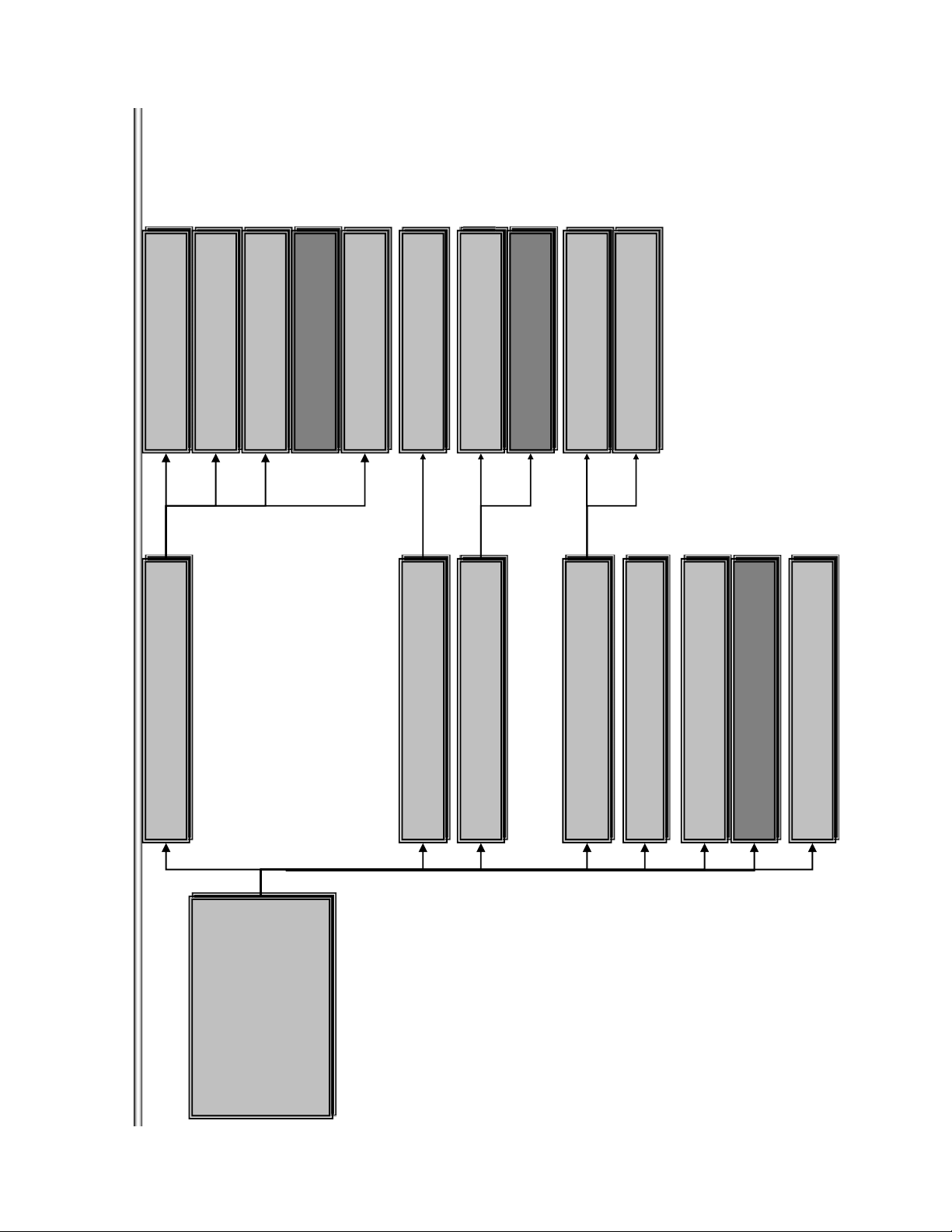
USB/ DA C/ IFCo n test
Devi ce Te st
~
Video Output Test
Video Test
~
Audio Output Test
Audio Test
~
Not used
~
Audio input Test
only wireless model used
Wir el ess LAN Test
~
view Erro r l o g
Error Log
~
Initialize default setting for BD-Player
St ar t I nit ial i ze
~
Not used
Start Initialize for TV
~
view Network Stat us
Ifconfig
~
confirm Net work con n ection
~
Ping
Menu
Dia g Test
*Diag
~
[7]ENC Test Mode
[8]Drive
[6]System Information
* Ser vi c e Mod e Men u
[1]Diag
[5]Version Up
[4]Network
[ 3]Factory Initialize
[2]Log
*Log
view Erro r Log
I nit iali ze default setti ng
* Factory Initialize
~
Network di agnosis f or w ir ed
*Network
~
DISC update
Ver sio n Up
~
di splay System I nfo rmation
Sy s t em I n f o r m a t ion
~
not used
EMC Test Mode
~
Write Drive OP Data and check drive
Drive
~
-
Page 73
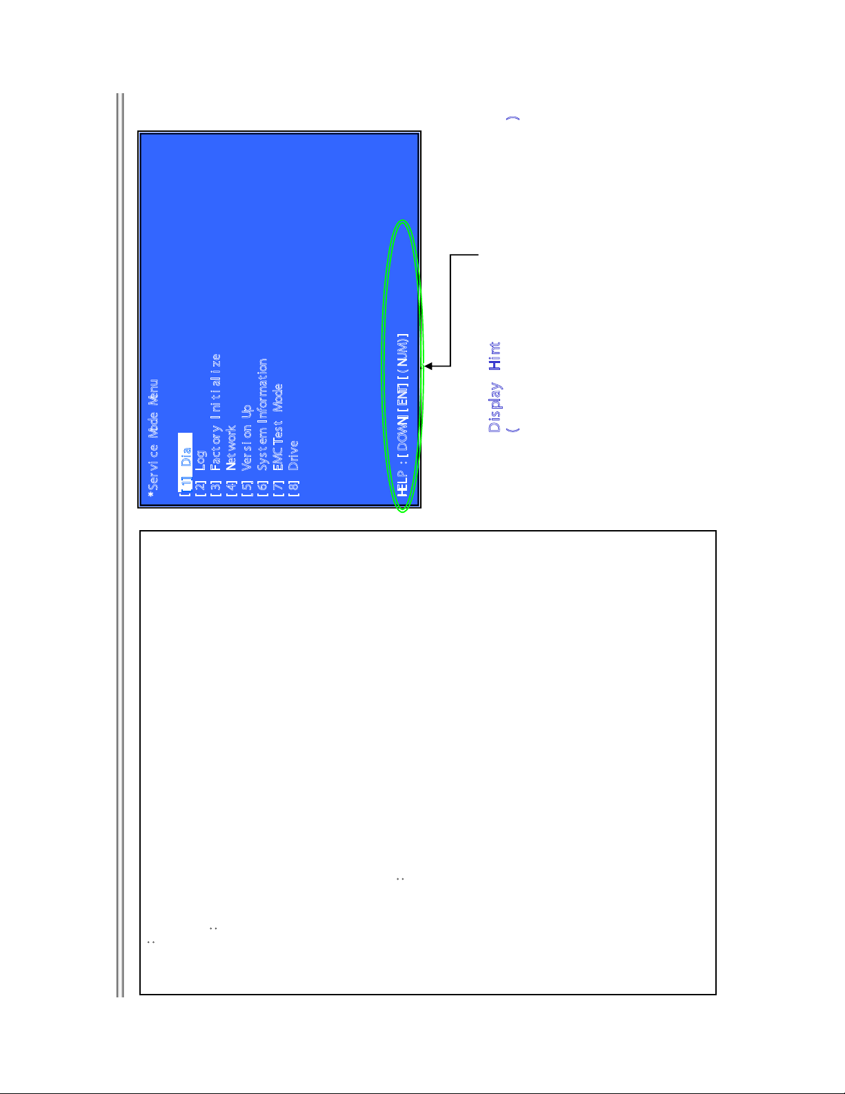
BDP-BX37/S270/S370/S373/S470
)
Dis play Hint
( The key in which the present use is possible
[ 1] Diag
*Ser vi ce Mode Menu
[ 1] Di ag
[ 2] Log
[ 3] Fact ory Ini t i al i ze
[ 4] Net work
[ 5] Ver si on Up
[ 6] Syst em Information
[ 7] EMC Tes t Mode
[ 8] Drive
Menu,
£
(not Used)
DISC version Up
¢
HELP : [ DOWN] [ ENT] [ ( NUM)]
S-LOG
S-DI AG
Outline
(4AE824 ">34 "4=D
Service Mode Top Menu
[ ENT] Activ ate t he sel ect ed cu r sor .
[1] Select and Activate Diag Menu.
I t selects t o each f un cti on f ro m here.
output HDMI /Component 480p f or cibly.
[ 2 ] Select and Acti vat e Log Menu,
Operation
[ 6 ] Select and Acti vate System In f orm at io n Menu.
[ 4 ] Select an d Act i vat e Net w o rk Menu
[ 3] Select and Activate Factory Initi alize Menu.,
[ 5 ] Select and Acti vat e Versi on Up
[DOWN] Move Down cursor
[ 7 ] Select and Act i vat e EMC Test Mode Menu .
[UP] Move Up cursor
[ 8 ] Select and Acti vat e Dri ve Menu.
Front Panel Display
I f cursor or arbi tra ry m enu keys are operated,
* the character str i ng.
*The cursor is not displayed when initial.
the character w i ll outp ut to a f r ont panel di splay, r espectively.
Factory Initialize: S-FINIT
Log
Diag
initial display SERVICE
Sy s t em I n f o r m a t ion: S- I NF O
EMC Test Mode: S-EMC
Ver sio n Up S-VUP
Network: S-NET
Drive: S-DRV
7-3
Page 74
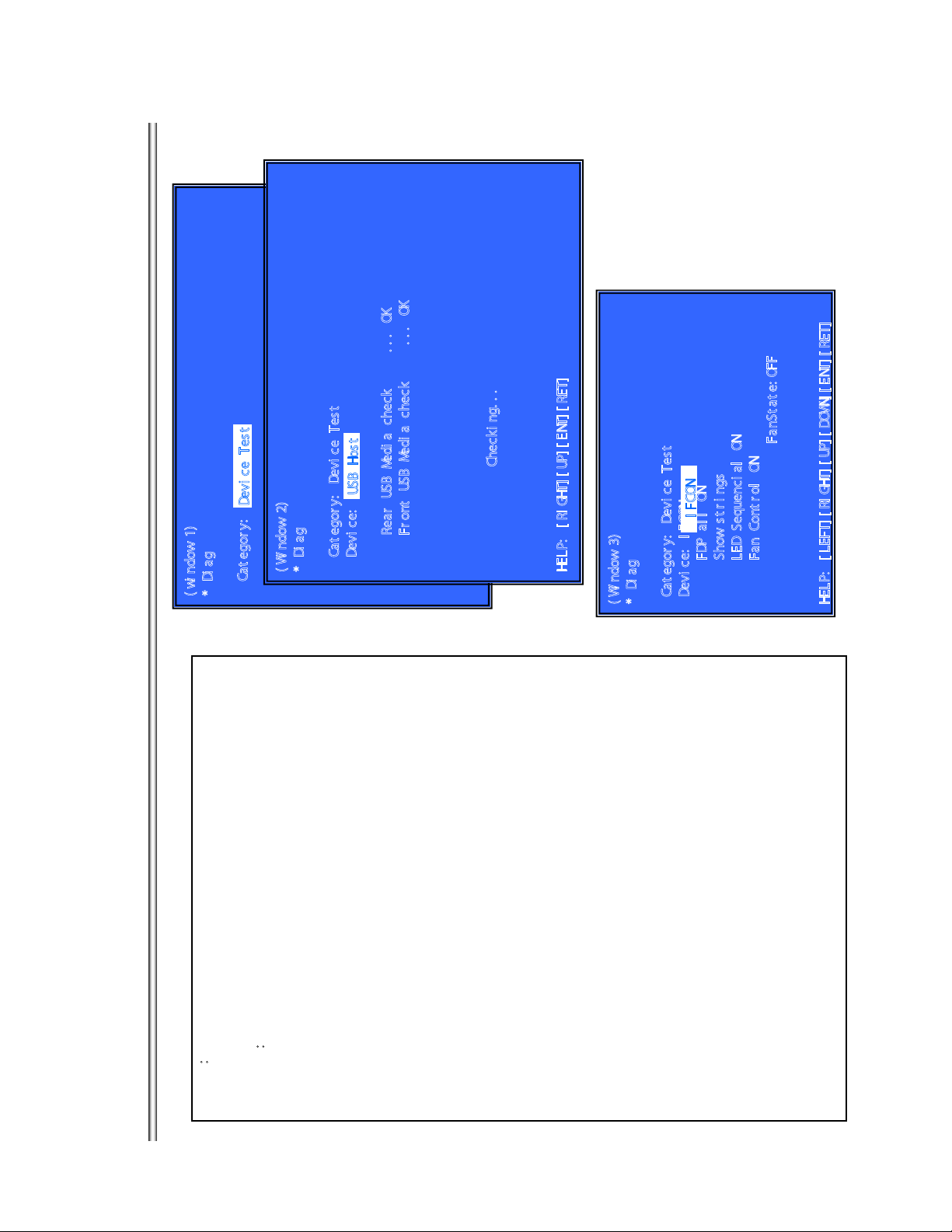
BDP-BX37/S270/S370/S373/S470
FanSt at e: OFF
Checki ng. . .
Devi ce Test
( Wi ndow 2)
( wi ndow 1)
Cat egory:
* Di ag
* Di ag
USB Host
ear USB Medi a check .. . OK
R
Fr ont USB Medi a check .. . OK
Cat egory: Devi ce Test
Devi ce:
HELP: [RI GHT] [ UP] [ ENT] [ RET]
( Wi ndow 3)
* Di ag
Only one time.
I FCON
FDP al l ON
Show st r i ngs
LED Sequenci al ON
Fan Contr ol ON
Cat egor y: Devi ce Test
Devi ce: IFCON
HELP: [LEFT] [ RI GHT] [ UP] [ DOWN] [ ENT] [ RET]
l ON
FanSt at e: OFF
Outline
The device carri ed i n t he substrat e is tested.
806"4=D (Device Test)
HT][UP][DOWN] [ ENT][RET]
IF select IFCON, Move Up cursor. (see windows 3)
LED Sequencial
Sh o w St r ings
FAN Control ON
FDP all O N
(Window 1) Select test category
Operation
[DOWN][ENT] Activate the selected Category.
[LEFT] [RIGHT] Select Category
After “Device Test” selects in window 1, the device to test is chosen.
Operation:
[RET] Return to Service Top Menu.
(Window 2) Device Test
[UP] Return to test category selection.
[LEFT][RIGHT] Select Device
[ ENT] Act i vat e an d Star t Test
[RET] Return to test category selection.
>Test category list
Devi ce Te st
Video Test
[DOWN] IF select IFCON, Move Up cursor. (see windows 3)
Audio Test
>Device Test :Device List
Audio Input Test (not Used)
USB Host USB Media Check (Front and Rear)
Wir el ess LAN Test (only Wireless Model)
D/A Converter DAC write check (non-verification)
IFCON IFCON Test (see windows 3)
Fan St a te (D i s p l a y )
7-4
Page 75
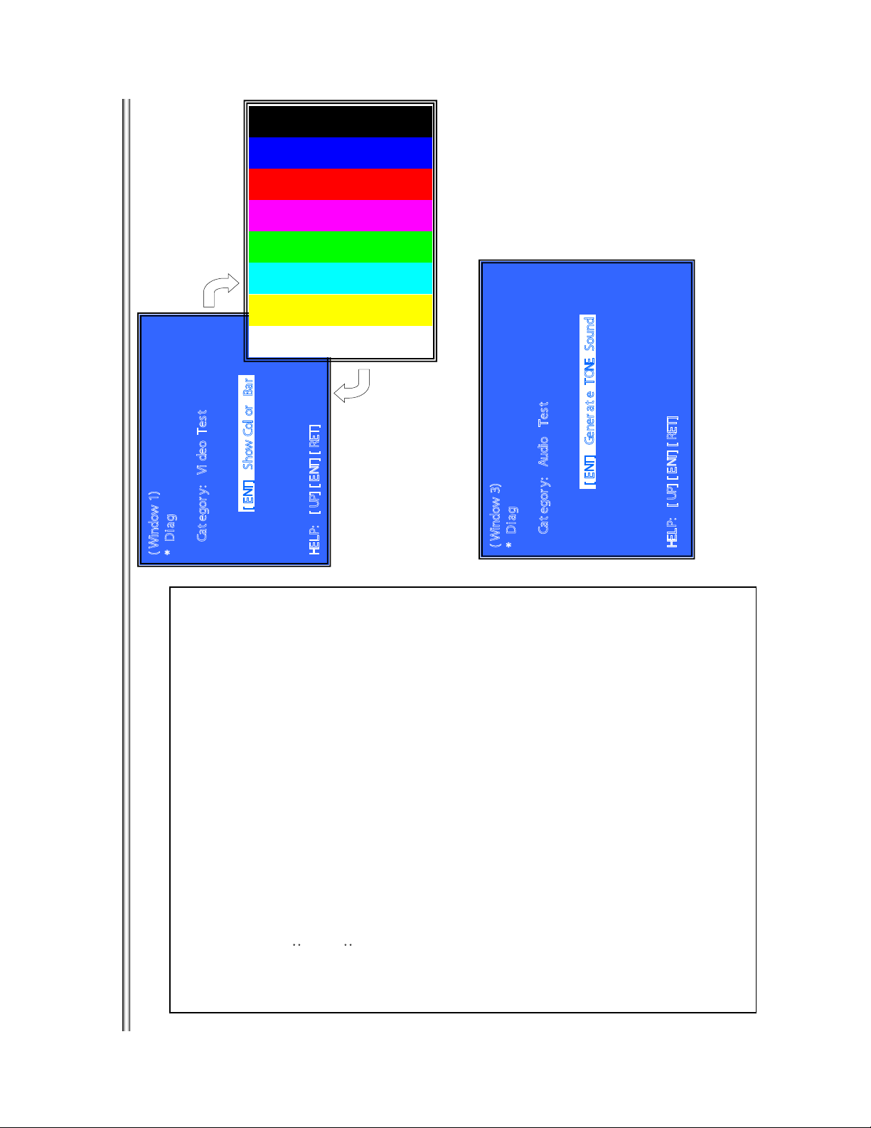
[ENT]
BDP-BX37/S270/S370/S373/S470
(Window 2)
[ENT]
[ ENT] Gener at e TONE Sound
[ ENT] Show Col or Bar
( Window 1)
Cat egory: Vi deo Test
* Diag
HELP: [UP] [ ENT] [ RET]
( Window 3)
Cat egor y: Audio Test
* Diag
HELP: [UP] [ ENT] [ RET]
[UP][RET] Return to test category selection.
(Window 1)Select Video Test Category
Outline:
Activate Video Test and Audio Test
Operation:
(Window 2)Display Color Bar
[ ENT] Acti vate and display Color Bar
806"4=D (Video Test/ Audio Test)
>Audio Test;
Operation
[ ENT] Return to Select Video Test Categor y.
(Window3 ) Select Audio Test Category
Operation
>Video Test:
[UP][RET] Return to Select Audio Test Category
[ ENT] Play TONE Sound/ Stop
TONE sound out p ut ineOut( 2ch) & / SPDIF & HDMI.
Color Bar output S terminal & composite & Component & HDMI.
7-5
Page 76
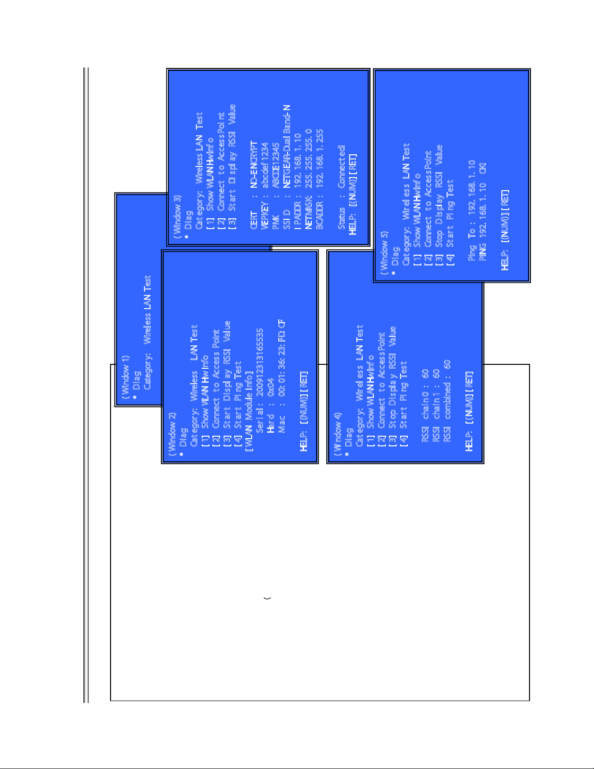
BDP-BX37/S270/S370/S373/S470
7
)] [ RET]
M
U
Cat egory: Wireless LAN Test
[ 1] Show WLAN HwInfo
[ 2] Connect to Acces sPoi nt
[ 3] St ar t Di spl ay RSSI Value
CERT : NO-ENCRYPT
WEPKEY : abcdef 1234
PMK : ABCDE12345
SSI D : NETGEAR-Dual Band- N
I PADDR : 192. 168. 1. 10
NETMASK: 255. 255. 255. 0
BCADDR : 192. 168. 1. 255
Status : Connect ed!
( Window 3)
* Diag
HELP: [(N
Ping To : 192. 168. 1. 10
Cat egor y: Wir el es s LAN Tes t
[ 1] Show WLAN HwInf o
[ 2] Connect to AccessPoint
[ 3] Stop Dis play RSSI Value
( Window 5)
* Diag
[ 4] St ar t Pi ng Tes t
PING 192. 168. 1. 10 OK!
HELP: [(NUM)] [ RET]
Diag Menu (Wireless LAN Test) <only Wireless Model>
Categor y: Wireless LAN Test
( Window 1)
* Diag
Cat egory: Wireless LAN Test
[ 1] Show WLAN Hw Info
[ 2] Connect to Acces s Point
( Window 2)
* Diag
[RET] Return to Service Top Menu.
[DOWN][ENT] Activate the selected Category.
(Window 1)Select Wireless LAN Test Category
Operation:
Outline:
[LEFT] [RIGHT] Select Category
Act i v at e Wi r el e ss LAN Test s
(Window 2) Select Wireless LAN Test
Operation:
[ 1] Show Wireless LAN module I nformation
[ 3] St ar t Displ ay RSSI Value
[ 3 ] Star t display RSSI value.
[2] Connect Access Point
[4 ] Start Ping Test
HELP: [( NUM) ] [ RET]
UM)] [ RET]
N
Ser i al : 200912313165535
Har d : 0x04
Mac : 00: 01: 36: 23: FD: CF
[ 4] St ar t Pi ng Tes t
[ WLAN Module Info ]
See Window 2)
[UP][DOWN] Select Test
[ ENT] Acti v ate and Star t Test
[RET] Return to test category selection.
> Show WLAN HwInfo ¢
HELP: [(
Mac Addr ess
Hard : Hardware Version
Mac
Ser i a l : Seri a l Nu mb e r
> Connect to AccessPoint (See Window 3)
Connect Access Point only wi th the fo llow ing AP sett ings.
Authentication method: NO-ENCRY P T
( Wi ndow 4)
abcde f1234
WEP key
* Diag
NETGEAR-DualBand-N
SSID
Cat egory: Wir el ess LAN Test
ABCDE12345
PMK
[ 1] Show WLAN HwInf o
[ 2] Connect to Acces sPoint
[ 3] St op Di s pla y RSSI Value
192.168.1.255
IP: 192.168.1.10
Net m ask: 255.255.255.0
Broadcast
RSSI chain 0 : 60
[ 4] St ar t Pi ng Tes t
When co nnect t o AP, Stat us i s “ Connect ed! ”
When cannot connect to AP, Status is “can’t Connect!”
~
RSSI chain 1 : 60
ue.
Display RSSI val
> Start Display RSSI Value (See Window 4)
)] [ RET]
M
U
N
RSSI combined : 60
HELP: [(
Ping Test.
I P address use the value of “192.168.1.10”.
> Start Ping Test (See Window 5)
7-6
Page 77
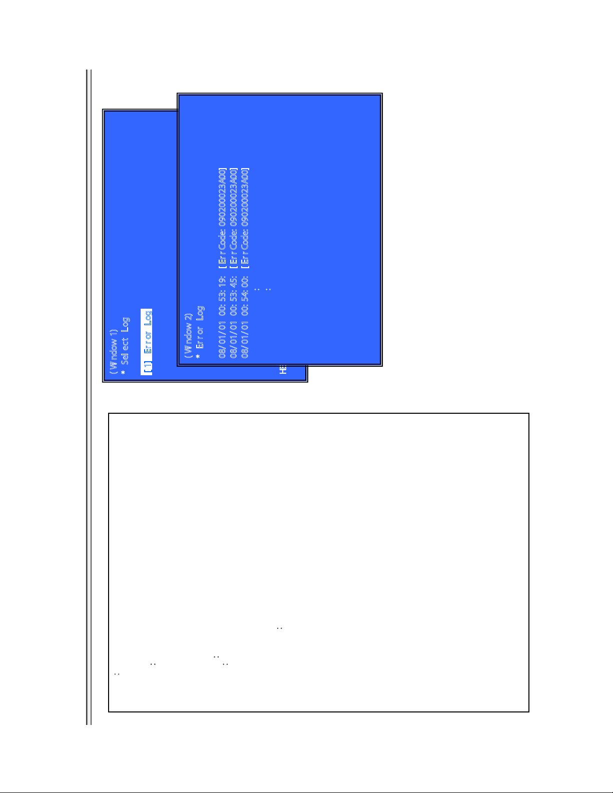
BDP-BX37/S270/S370/S373/S470
:
:
( Wi ndow 2)
* Er r or Log
08/ 01/ 01 00: 53: 19: [Er r Code: 090200023A00]
08/ 01/ 01 00: 53: 45: [Er r Code: 090200023A00]
08/ 01/ 01 00: 54: 00: [Er r Code: 090200023A00]
( Wi ndow 1)
[ 1] Er r or Log
* Sel ect Log
HELP : [DOWN] [ ENT] [ ( NUM) ]
S-ELOG
!>6 : AA>A !>6
Display Error Log
08/01/01 00:53:19: [ErrCode :080400000000]
[Date] [Time] [ErrCode]
Please do not pull out USB memory immediately after the RED button was pushed.
Please do not push the RED button immediately after USB memory is inserted.
[DOWN] Move Down cursor
Outline
Display each co nt e n t s o f t h e Erro r lo g ,
[UP] Move Up cursor
(Window 1) select log.
Operation
[ 1] Activate and Display Error log
(Window 2)
[ ENT] Acti v at e t h e select ed cur sor .
[RET] Return to Service Top Menu.
[RIGHT] Previous Page
Operation
[LEFT] Next Page
[ RET] Return to select log (window 1)
Front Panel Display
[ RED] Wr i t e th e con te nt s o f an er r or l og on a USB memo ry .
select log Error Log
Display Page display page ex) 001 / 050
>Log contents
Error Log
**Write the contents of a log on a USB memory**
[ RED] is pushed where a USB memory is inserted in a set in log display screen.
“getErrLogFile.trm” f ile is outputted in a USB memory.
Error Log:
7-7
Page 78
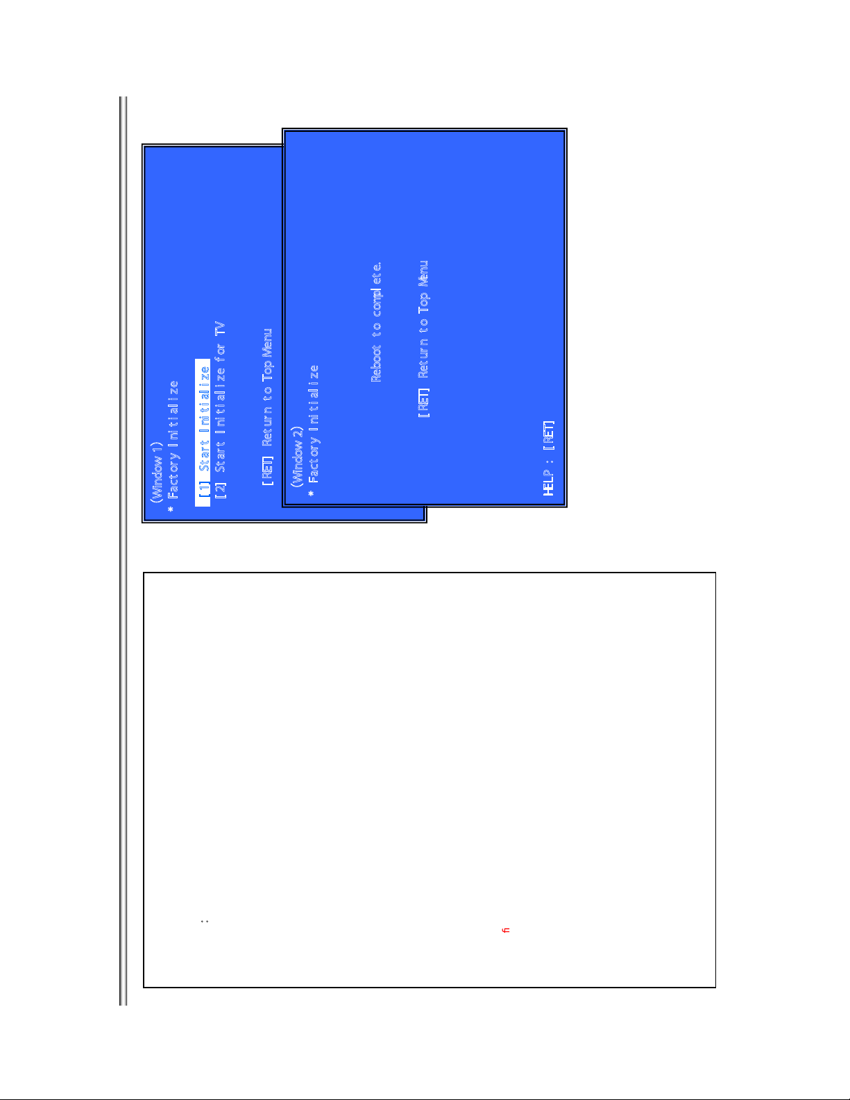
BDP-BX37/S270/S370/S373/S470
Reboot to compl et e.
[ RET] Ret ur n to Top Menu
¢Window 1£
[ RET] Ret ur n to Top Menu
¢Window 2£
[ 1] St ar t Ini t i al i ze
[ 2] St ar t Ini t i al i ze for TV
* Fact or y Ini t i al i ze
HELP : [RET]
* Fact or y Ini t i al i ze
(not used)
INIT-NG
I NIT-OK (window 2)
SETTING
[ 1] Start Factory Initialize
Outline:
Return al l of the pl ayer setti ng to th eir f actor y defaults .
(Window 1) select initialize.
[ 2] Start Factory Initialize for TV
Operation
When you return a set to the factor y defaults, push [ 1 ] on this screen.
[UP] Move Up cursor
[DOWN] Move Down cursor
02C>AH =8C80;8I4
[RET] Return to Service Top Menu.
Please discon nect AC pow er suppl y, and conn ect AC again .
[RET] Return to Service Top Menu.
[ ENT] Act i vat e th e sel ecte d cur so r .
(Window 2)
It is a screen of the end of initi alization.
- The operation of other servi ce mode menu can be conti nued.
Initialize NG
Initialize OK
Front Panel Display:
Initialize
rm the following processes for all sets.
neede d.
Please con
Caution:
When “Quick Stand By” sets ON, The addit ional processes of AC I N and OFF are
1. Ini t i ali ze (This command)
5. AC Off
6. AC In
4. Check FLD. If WAIT keep bl i nking, go to 5. el se go to 8.
2. AC Off
3. AC In
7. Check FLD.
8. AC Off. (finish)
7-8
Page 79
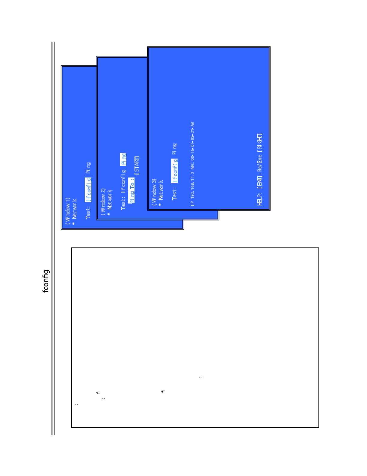
BDP-BX37/S270/S370/S373/S470
Pi ng
[ START]
I f conf i g
I f conf i g
( Wi ndow 2)
£
Display networ k setti ng
¢
* Net wor k
( Wi ndow 1)
Test : Pi ng
* Net wor k
Pi ng To :
Pi ng To :
Test : If conf i g
( Wi ndow 3)
Test : Pi ng
* Net wor k
I P 192. 168. 11. 2 MAC 00- 16- 01- 85- 21- A3
HELP: [ENT] : Re/Exe [RI GHT]
#4CF>A: ¢Network Test: £
S-NET
g Test Active
:
(Window 2)Ping Test
Operation:
[ LEFT] Select I f co nf i g Test .
[ RET] Retur n t o Servi ce To p Menu.
(Window 3)Ifcon
Outline
Network Menu for the wired Ethernet.
(Window1)Ifcon g Test
Operation
[ ENT] Acti vat e I f co nf ig
[ RI GHT] Select Ping Test .
[RET] Return to Service Top Menu.
(The details of a Ping test are nest page)
[ENT] Ifconfig retry
[ RI GHT] Select Ping Test .
[ RET] Retur n t o Servi ce To p Menu.
Operation
Display Ifconfig command results.
Front Panel Display
7-9
Page 80
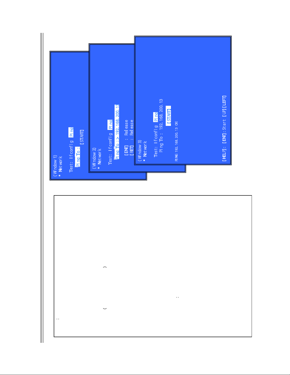
BDP-BX37/S270/S370/S373/S470
Pi ng
[ START]
Pi ng
Pi ng
[ START]
[ ENT] : Rel ease
[ RET] : Rel ease
[ LEFT] : If conf i g Test
Pi ng To :> 192. 168. 200. 13
Pi ng To :
Pi ng To :
Pi ng To :
Test : If conf i g
( Wi ndow 1)
* Net wor k
( Wi ndow 2)
Test : If conf i g
* Net wor k
[ ( NUM) ] : ‘ 0- 9’
( Wi ndow 3)
* Net wor k
Pi ng To : 192. 168. 200. 13
[ TI ME] : ‘ . ’
[ CLEAR] : Backs pace
Test : If conf i g
PI NG 192. 168. 200. 13 OK!
[ HELP] : [ENT] : St ar t [UP] [ LEFT]
#4CF>A: ¢Netwrok Test: %8=6£
S-NET
IP address input mode £
¢
[CLEAR] Backspace
(Windows3): Ping Test Active
[ TIME] I nput Character sting ’.’
[ (NUM)] Input Character sti ng ‘0 -9’
[ LEFT] Finish to input and Select If confi g Test.
Outline
Ping Test f or the wired Ethernet.
(Window 1)Ping Test
Operation:
[ LEFT] Sele ct I f conf i g Test .
[DOWN] Ping executi o n preparation.
[ RET] Retu r n t o Serv ice Top Menu.
(Window 2) The IP address of the Ping point is set up.
[ RET] Finish to input.
When “Ping to : >” i s reversed, [ENT] is pushed and I P is inputted.
Operation:
[ ENT] Finish to input.
When [ START] i s reversed, [ENT] i s pushed and execute ping .
[ RET] Retu r n t o Servi ce Top Menu.
[ UP] The IP address of the Ping point is set up.
Operation:
[ ENT] Activate Ping Test
Front Panel Display
7-10
Page 81
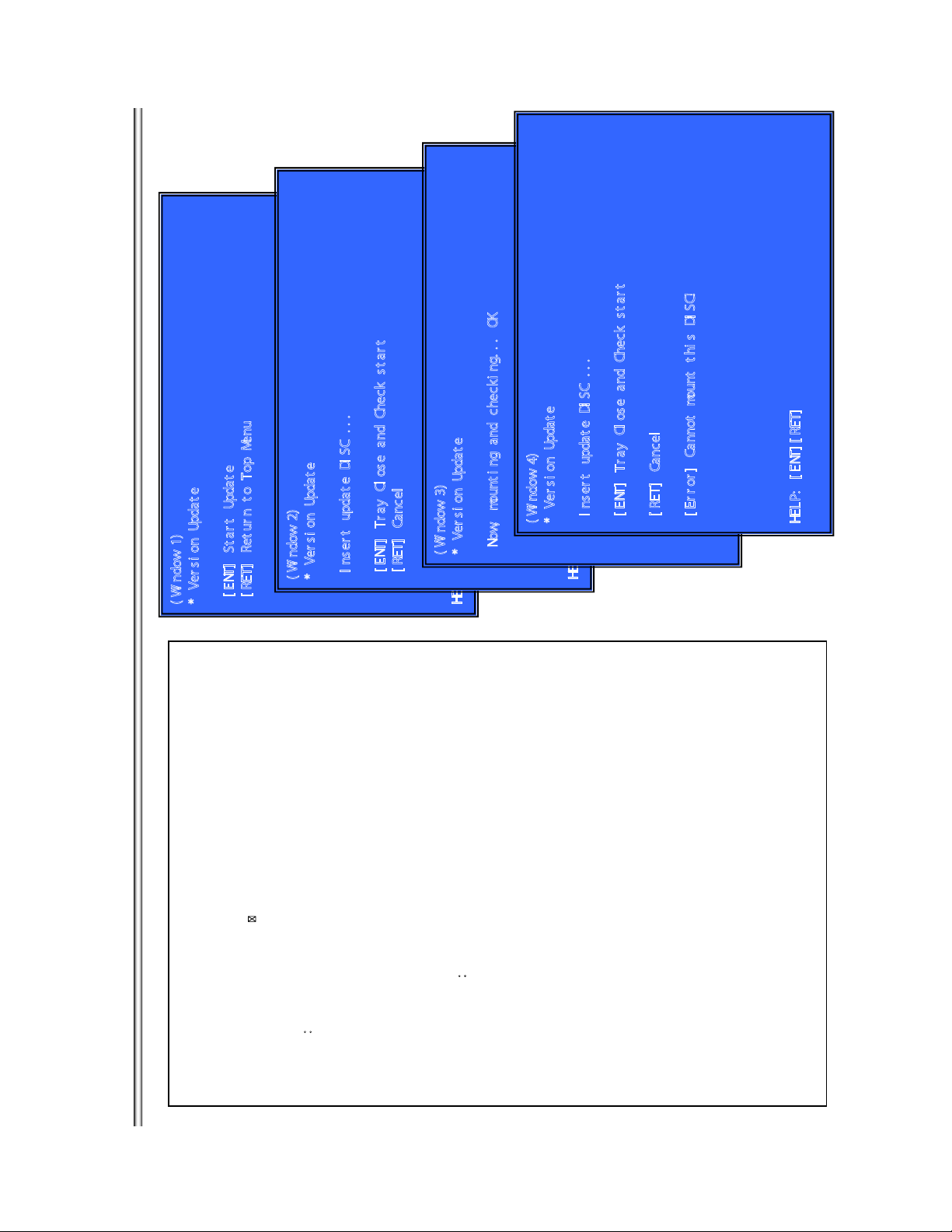
BDP-BX37/S270/S370/S373/S470
I nser t updat e DI SC .. .
[ ENT] Tr ay Cl ose and Check st ar t
[ RET] Cancel
( Wi ndow 4)
* Ver si on Update
( Wi ndow 3)
I nser t updat e DI SC .. .
[ ENT] Tr ay Cl ose and Check st ar t
( Wi ndow 2)
* Ver si on Update
[ ENT] St ar t Updat e
( Wi ndow 1)
* Ver si on Update
[ RET] Ret ur n to Top Menu
[ RET] Cancel
and w ait .
£
error messag e
KKK¢
Now, mount i ng and checki ng. . . OK
* Ver si on Update
HELP: [ENT] [ RET]
HELP : [ENT] [ RET]
[ Er r or ] Cannot mount thi s DI SC!
HELP: [ENT] [ RET]
+4AB8>= *? ¢using Update (£
[Error]
After reboot, please open tray and eject Update Disc manually.
: star t update sequence automati cally and reboot.
(Window 3) Disc Check and OK (Right DISC)
[ RET] Retur n t o Servi ce To p Menu.
(Window 1)Version Up Menu
Outline:
update softw are using DISC
Operation:
(Window 2) Place the Update Disc
[ENT] Start Update (Tray Open and go to window 2 )
Operation
[ENT] Tray Close an d check DISC.
Operation
[RET] Cancel Update (Tray Close and return to window 1)
(Window 4) Disc Check and NG (not update DISC)
Operation:
open tr a y aut o mat i cal l y.
DI SC Che ck O K V- CHK O K
DI SC Che ck N G V-CHKN G
Can’t Mount V-NODSC
Front Panel Display
DISC Insert V-INSCD
7-11
Page 82
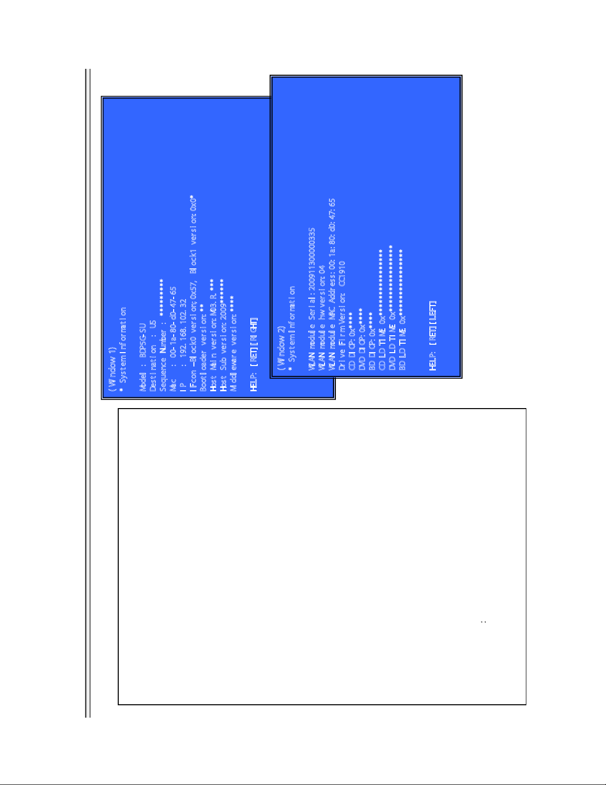
BDP-BX37/S270/S370/S373/S470
( Wi ndow 2)
* Syst em Inf or mat i on
WLAN modul e Ser i al : 200911300000335
WLAN modul e hw versi on: 04
WLAN modul e MAC Address: 00: 1a: 80: d0: 47: 65
Dr i ve Fi r m Ver si on: CC1910
CD DI OP: 0x* * **
DVD DI OP: 0x* ***
BD DI OP: 0x* ***
CD LD TI ME 0x****** **** **** **
DVD LD TI ME 0x* **** **** **** ** *
BD LD TI ME 0x****** **** **** **
( Wi ndow 1)
* Syst em Inf or mat i on
Model : BDP5G- SU
Des t i nat i on : US
Sequence Number : *** ***** *
Mac : 00- 1a- 80- d0- 47- 65
I P : 192. 168. 102. 32
I Fcon –Bl ock0 ver si on; 0x57, Bl ock1 versi on: 0x0*
Boot l oader ver si on: **
Host Mai n ver si on: M03. R. ***
Host Sub ver s i on: 2009***** *
Mi ddl ewar e ver s i on: ****
HELP: [RET] [ RI GHT]
(only wireless model)
(only wireless model)
(only wireless model)
displayed. (go to window 2)
Wireless device Inf orm ati on ( onl y wi reless model)
HELP: [RET] [ LEFT]
IOP
(Window 1)Basic Information Menu
Outline:
Disp l ay Syste m Inf or m at io n
Operation:
[ RET] Retur n t o Servi ce To p Menu.
[RI GHT] Dr i ve I nf o r m ati o n (del t a IOP of a dri ve i s m easu r ed ) and
(HBC4< =5>A<0C8>=
(Window 2)Drive and Wireless Information Menu
[ RET] Retur n t o Servi ce To p Menu.
Operation:
[ LEFT] Basic Info rm ati on di splayed. ( go to wi ndow 1 )
When delta IOP is measured, it becomes impossible to use the Version Up function.
Contents List:
Model
Sequence Number
MACIPIFCON IFCON Version
Destination
Host Su b Host Sub Ve rsion
Boo t l oa de r Boo tl o ad er Ve r si on
Host Main Host Main Version
WLAN module hw ve rsion
Middleware Middleware Version
WLAN module MAC Address
Drive Firm Revision
WLAN module Serial
CD LD TIME LD T ime
BD DIOP Del t a
DVD DIOP Delta IOP
CD DIOP Delta IOP
Front Panel Display
BD LD TI ME LD Time
DVD LD TIME LD Tim e
Display Host Main Version
7-12
Page 83
BDP-BX37/S270/S370/S373/S470
BD modulation frequency
Mode 1 --> 410Mhz
Able to select mode 1 or 2
Mode 2 --> 429Mhz
*Service Menu
[1]Diag
Screen 1
[2]Log
[3]Factory Initialize
[4]Network
[5]Version Up
[6]System Information
[7]EMC Test Mode
[8]Drive
Screen 2
*Drive
[1]Drive OP data Write
[2]Servo Parameter Check Menu
[5]Readability Check Menu
[6]OP Position Check Menu
[7]OP Check Menu
[8]Load Eject Aging
[9]Spindle Control Check Menu
[3]Servo Signal Check Menu
[4]S - Curve Check Menu
: D-READ
[10]FA Test Mode
Screen 3
*Drive OP data Write
Insert USB StorageDevice ...
[ 2 ] Mode: 1
Remove DISC and Close tray.
[1]Disc: Eject
[ENT] Start
Drive
Overview:
This menu is used to operate the drive using drive-related diagnostic
and tools.
Screen 1: Selecting items under *Service Menu
Screen 2: Selecting items under *Drive
Operations:
[UP] [DOWN] Move the cursor up and down
[ENT] Open the selected cursor item
[RET] Return to top menu
Test item list Display Panel
[1] Drive OP data Write : D-OPWRT
[2] Servo Parameter Check Menu : D-SEVPA
[3] Servo Signal Check Menu : D-SEVSG
[6] OP Position Check Menu : D-OPPOS
[4] S-Curve Check Menu : D-SCUR
[5] Readability Check Menu
7-13
[7] OP Check Menu : D-OP
[8] Load Eject Aging : D-LOAD
[9] Spindle Control Check Menu : D-SPIND
[10] FA Test Mode : D-FAMOD
Screen 3: *Drive OP data Write
Purpose: Write OP data into flash IC
[UP] [DOWN] Move the cursor up and down
[ENT] Start the selected cursor item
[RET] Return to top menu
Remarks:
Mode 1 --> Basic & Entry model (BD modulation frequency 410Mhz)
Mode 1 --> Step Up model (BD modulation frequency 429Mhz)
Page 84

BDP-BX37/S270/S370/S373/S470
r
u
Screen 4
*Servo Parameter Check Menu
[1]Disc : Eject
[2]Show Parameters
Screen 5
*Servo Signal Check Menu
[1]Disc : Eject
[2]Servo Signal Monitor out : OFF
[3]RTADJ : OFF
[4]FocusBias : 0000
[5]SA - Act.move : FWD 00 step
[6]PI Level : 0000
[7]RF Level : 0000
[8]TRV Level : 0000
[9] Current FB : 0000 SA : 0000
Not Use
Screen 6
*S - Curve Check Menu
[1]Disc : Eject
[2]Media Type : BD - ROM SL
[3]Layer : L0
[4]SLD move to Home
[5]SLD move : FWD 00 step
[6]FCS Search start
Drive
Purpose: Verify servo paramete
Screen 4: *Servo Parameter Check Menu Not Use
[UP] [DOWN] Move the cursor up and down
[LEFT] [RIGHT] Move the cursor left and right
[ENT] Start the selected cursor item
[RET] Return to top menu
Screen 5: *Servo Signal Check Menu Not Use
Purpose: Verify servo signal
[UP] [DOWN] Move the cursor up and down
[LEFT] [RIGHT] Move the cursor left and right
[ENT] Start the selected cursor item
[RET] Return to top menu
Screen 6: *S-Curve Check Men
Purpose: Verify S-Curve signal
7-14
[UP] [DOWN] Move the cursor up and down
[LEFT] [RIGHT] Move the cursor left and right
[ENT] Start the selected cursor item
[RET] Return to top menu
Page 85
BDP-BX37/S270/S370/S373/S470
Screen 7
*Readability Check Menu
[1]Disc : Eject
BD : x[xx]
DVD : x[xx]
CD : x[xx]
TEMP : xx.x deg
BD : xxxxh xxm
DVD : xxxxh xxm
CD : xxxxh xxm
[2]Address : 00000000
[3]Length : 0000
Jitter P: 0000
[4]Execute
SER: 0000 0000
Jitter PR: 0000
Jitter DC: 0000
Screen 8
*OP Position Check Menu
[1]Disc : Eject
[2]OP Position Check
Screen 9
*OP Check Menu
Remove DISC and Close tray
[1]Disc Eject
[2]OP Serial : xxxxxxxxxxxxxx
[3]dIOP
ed such as delta IOP and LD time
[4]LD ON Time
Drive
Screen 7: *Readability Check Menu Not Use
Purpose: Verify readability data
[UP] [DOWN] Move the cursor up and down
[LEFT] [RIGHT] Move the cursor left and right
[ENT] Start the selected cursor item
[RET] Return to top menu
Screen 8: *OP Position Check Menu Not Use
Purpose: Verify OP position
[UP] [DOWN] Move the cursor up and down
[LEFT] [RIGHT] Move the cursor left and right
[ENT] Start the selected cursor item
[RET] Return to top menu
Purpose: Verify OP relat
Screen 9: *OP Check Menu
7-15
[UP] [DOWN] Move the cursor up and down
[ENT] Start the selected cursor item
[RET] Return to top menu
Page 86
BDP-BX37/S270/S370/S373/S470
Screen 10
*Load Eject Aging
[1]Disc : Eject
Screen 11
*Spindle Control Check Menu
[1]Disc : Eject
[2]rpm : 0000 rpm
[2]Repeat set : 00000
[3]Mecha type : Tray mecha
[4]Aging type : Normal
[5]Start
[3]Spindle : OFF
Screen 12
aging
Repeat number : 0000
*FA Mode Test
[1]Enter Repeat FA mode
[2]Save FE log to USB
Drive
Screen 10: *Load Eject Aging Not Use
Purpose: Perform load eject aging
[UP] [DOWN] Move the cursor up and down
[LEFT] [RIGHT] Move the cursor left and right
[ENT] Start the selected cursor item
[RET] Return to top menu
Screen 11: *Spindle Control Check Menu Not Use
Purpose: Verify spindle rotation
[UP] [DOWN] Move the cursor up and down
[LEFT] [RIGHT] Move the cursor left and right
[ENT] Start the selected cursor item
[RET] Return to top menu
Screen 12: *FA Mode Test Not Use
Purpose: Perform FA(Drive)
7-16E
[UP] [DOWN] Move the cursor up and down
[ENT] Start the selected cursor item
[RET] Return to top menu
Page 87
BDP-BX37/S270/
S370/S373/S470
SECTION 8
ERROR LOG LIST
note
orInfo_0: LUN number
Other Error0x**
flash erase error
Other Error
Other Error
flash write error
)
Cannot detect optical drive
Other E rror
SATA IF ERROR
Other Error
SATA cable disconnected
Temperature is too high
Can not change fan state
0x00
0x00
Other commands read error
Disc read error
ErrorInfo_1: LBA address
ErrorInfo_0: LUN number
ErrorInfo_1: LBA address
Err
ErrorInfo_3: bNumConfigurations
ErrorInfo_2: bDeviceProtocol
ErrorInfo_1: bDeviceSubClass
ErrorInfo_0: Device Class
0x00
0x00
Error Sense Key
Error Code
Error Code
0x**
Error LogCode
0x02
Category ErrorCode ErrorInfo_ 0 ErrorInfo_1 ErrorInf o_2 ErrorInfo_ 3
0x04 0x00 0x00 0x00 0x00 0x00 NAND initialization failed
0x04
0x03
0x**
flash offset(0~~MAX_FLASH_SIZE
flash offset(0~~MAX_FLASH_SIZE)
0x01
0x05
0x010x06
0x02
0x05
0x05
0x**
0x00
SCR Diag Field(Simultaneous error)
0x020x06
0x030x06
0x01 0x01
0x06
0x07
0x**
0x**
0x**
Read Error LBA
0x00
0x**
0x01 0x02
0x01
0x07
0x08
0x09
Cmd
0x02
0x09
0x0A
issue
Error Log Information
DDR2 Error
CXD9983/CXD9984 Error 0x01
Ifcon Error
Ifcon transmition time out 0x03 0x01 0x00 0x00 0x00 0x00 No response from Ifcon
NAND Init Fail
NAND Error
NOR write Error
Nor Error
Drive Error
Drive Error
NOR Erase Error
Drive Error
8-1
Drive Error
Fan Error
Fan Error
Ethernet Error
MEDIA-OPTICAL DISC
MEDIA-OPTICAL DISC
USB media write error 0x0A 0x02 0x1 0x1 0x00 0x00
USB media read error 0x0A 0x01 0x1 0x1 0x00 0x00
Unsupported USB device 0x0A 0xFF 0x1 0x1 0x1 0x1
USB error
Page 88
BDP-BX37/S270/S370/S373/S470
History
ver 0.10 2009.11.16 Manak First release
ver 0.20 2010.01.13 Manak Add Caution for Factory Initialize
8-2E
Page 89

SECTION 9
TROUBLESHOOTING
Main Flow ............................................................................... 9-2
Power (System) Flow ............................................................. 9-3
IFcon Section Flow Chart (1/2) ............................................... 9-4
IFcon Section Flow Chart (2/2) ............................................... 9-5
Audio section flowchart........................................................... 9-6
Video section flowchart ........................................................... 9-7
SWP/SWB Board flowchart ................................................... 9-8
FR Board flowchart (1/2) ....................................................... 9-9
FR Board flowchart (2/2) ...................................................... 9-10
FR White LED ....................................................................... 9-11
Drive flowchart
Fan flowchart .......................................................................... 9-13
Ethernet flowchart................................................................... 9-14
USB (Front) Device Flow........................................................ 9-15
USB (Rear) Device Flow......................................................... 9-16E
........................................................................
9-12
BDP-BX37/S270/S370/S373/S470
9-1
Page 90
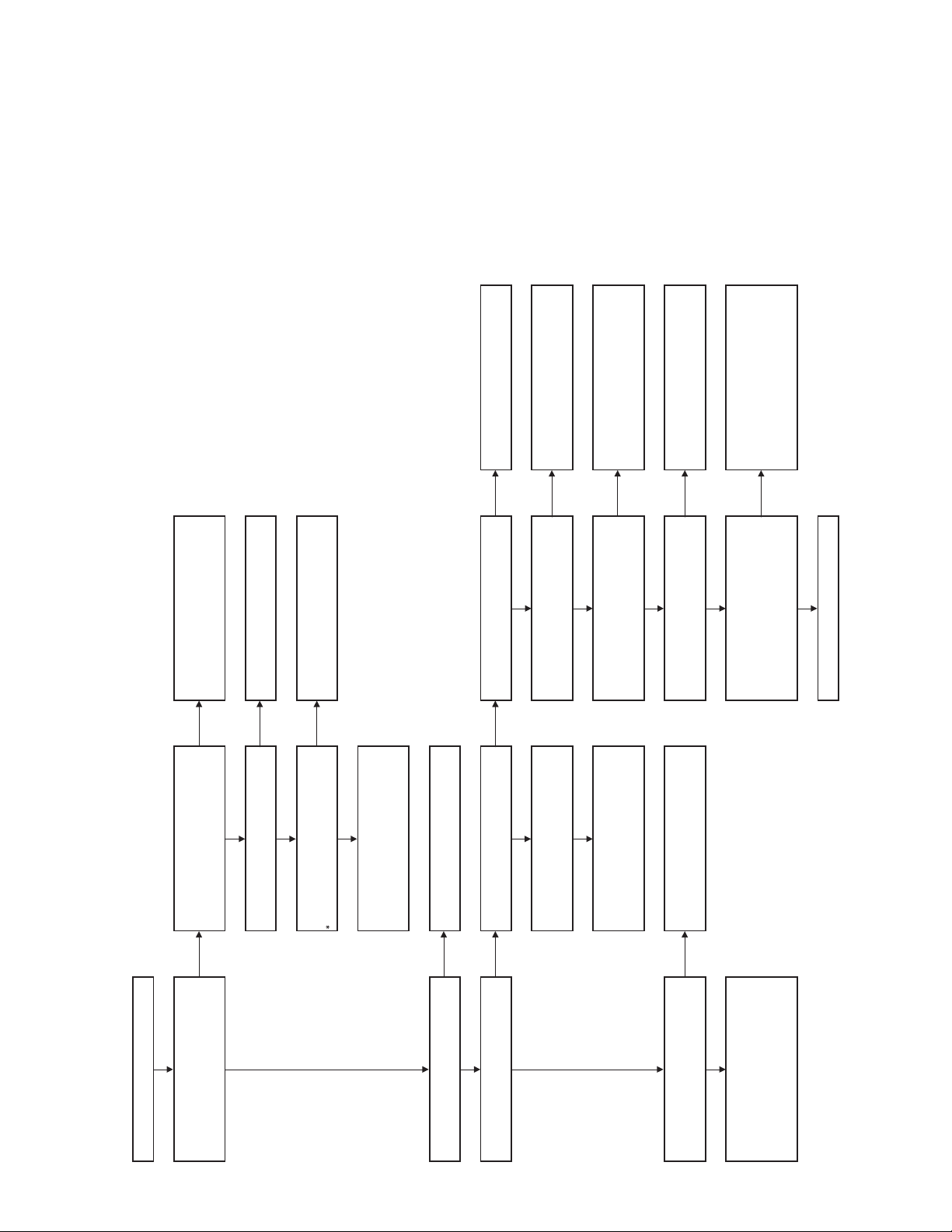
BDP-BX37/S270/S370/S373/S470
To Power Supply (System) flowchart.
Check the parts and mounting around X401.
No
To IFcon section flowchart
No
Yes
Yes
To Video section flowchart
Is XMB or the SETUP screen displayed on the
video output screen?
To FL/FR board flowchart
No
Do the up, down, left, and right arrow keys of
the remote control permit operations on the
XMB?
To Drive flowchart
No
Yes
Are BD, DVD, or other discs that are loaded on
the drive recognized correctly?
Yes Yes
To Audio section flowchart
Is the sound reproduced properly when a BD,
DVD, or other disc is played?
To Video section flowchart
No
Yes
END
Is the picture reproduced properly when a BD,
DVD, or other disc is played?
Are the power supply voltages on the MB
board normal?
No No
Start (and return from each flowchart)
Approximately 10 seconds after the AC is
applied, the WAIT display flashes several
times and the power is turned OFF
Main Flowchart
automatically.
Measurement point JL1122
Has system reset (PU_XRST) been
Is the main clock (X401) oscillating properly at
27 MHz?
Yes Yes
cancelled?
Replace the MB board.
To Drive flowchart
BU Adjustment Flow [yy] ~ After BU/MB
Replacement ~
No
Power ON by power switch on front or remote
Is OPEN or CLOSE displayed on the
To FR board flowchart
control.
fluorescent tube?
No No No
Yes
SYS ERR display appears on fluorescent tube.
9-2
Replace the MB board.
To Drive flowchart
BU Adjustment Flow [yy] ~ After BU/MB
Is there any problem in the FFC connection to
CN2470 which connects the drives?
Yes Yes Yes
Replacement ~
To Drive flowchart
No No
Yes Yes
Check the flexible cable of the drive.
Are CN2470,CN2462 or CN1401
disconnected?
Check the connections of the connectors.
If there is no improvement, replace the MB
board.
To Drive flowchart
BU Adjustment Flow [yy] ~ After BU/MB
Replacement ~
Page 91
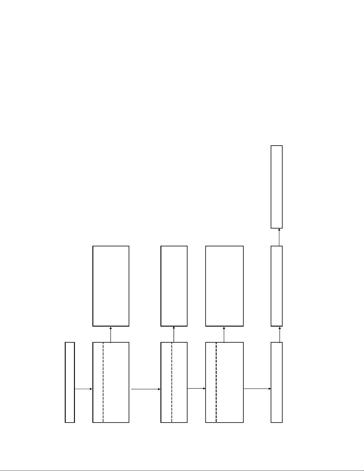
BDP-BX37/S270/S370/S373/S470
y
Replace the MB board if there is no
Failure of power supply IC -> Replace the IC
No
power supply block.
Check that the harness has been inserted
properly. If there is no problem, replace the
No
AC IN
Yes
No
Replace blown fuses
Replace the MB board if there is no
improvement
Yes
No
To IFcon section Flow
Yes
Voltage lines that are not output are shorted
to GND
No
block.
Power (System) Flow
Check the output voltages from the power
suppl
CN301 pin 1: +12V (UNSW12V)
CN301 pin 2: +12V (FE_UNSW12V)
CN301 pin 6: +5.8V (FE_UNSW6VA)
CN301 pin 7,8,9: +5.8V (UNSW6V)
CN301 pin 10:-6V(UNSW-6V)
MB board: PS301, PS302, PS303, PS304,
PS802
Check the fuses
Have any of the below fuses blown?
FR board: PS701
Check the following power control signals
while the power is ON
PCONT_CORE: MB board R327
PCONT2: MB board R318
PCONT3: MB board
R305,R307,R306,R309,R343,R329
ATA_PCONT: MB board R376
Check the voltages based on the schematic
diagram
9-3
Page 92
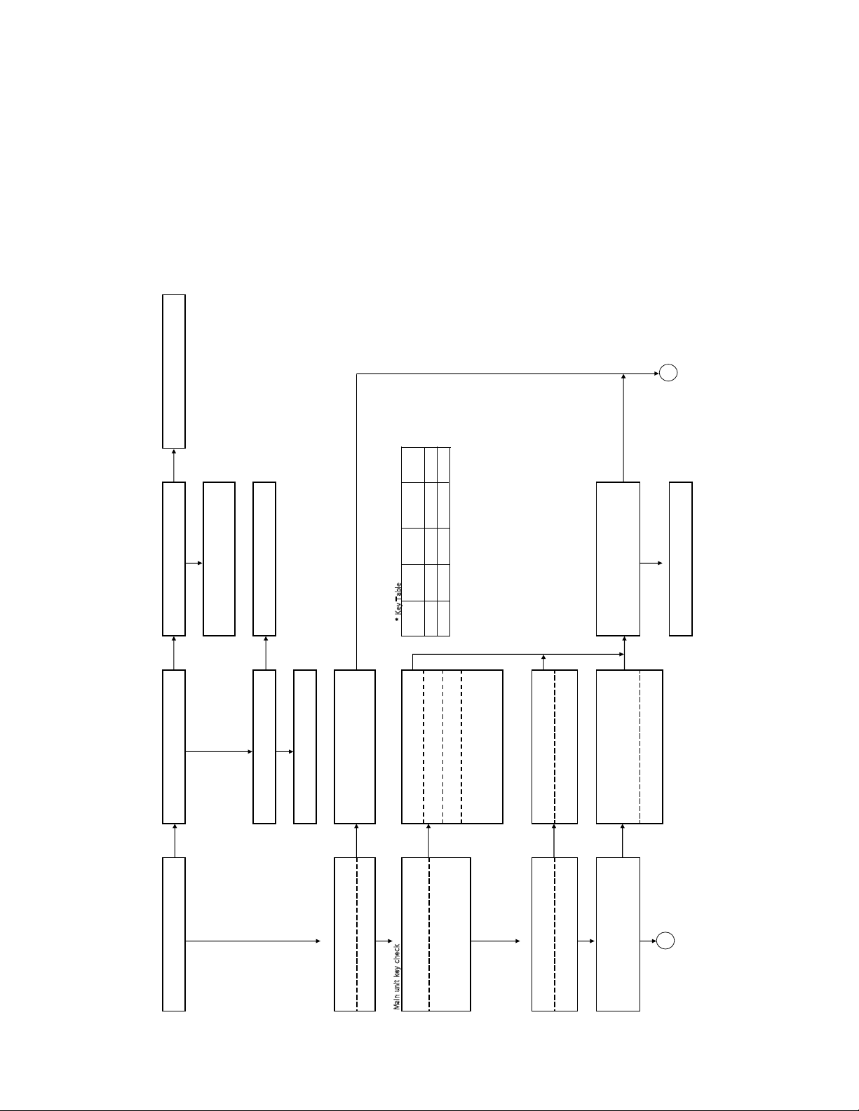
p
pp
y
k
h
k
tl ?
BDP-BX37/S270 /S370/S37 3/S470
B
No
No
Input voltage
To Power Supply (System) flowchart
Is the fuse (PS301) blown?
Is +5.8V input to IC301 pin5?
Replace PS301
If symptoms do not improve, check for a
Yes Yes
short on the circuit board
Replace IC301
No
REG control voltage
Is +5.8V input to IC301 pin1?
Yes
Replace R302
If symptoms do not improve, replace IC301
±
PLAY
°
(KEY2) (KEY3 )
Key_OFF Key_OFF
°OPEN/CLOSE ±
Key_OFF
°STOP ±
(KEY0) (KEY1)
ble
Key_OFF
Input
No
(Other than the POWER key)
Is the FFC from CN1509 disconnected?
2.90 -
Is the harness from CN1509 disconnected?
°POWER±
0.00 -
(POWER key)
Is the SWP-001 harness from the power
supply disconnected? (POWER key)
No
Check whether the FFC is disconnected
from CN1504. (Other than the POWER key)
condition of C1513, 1514, 1515 or 1516?
Is there a problem with the mounting
condition of RB1502 or 1501?
Is there a problem with the mounting
Is there a problem with the RB1503
mounting condition?
a
ey T
K
*
Replace R1564 and check for +3.3V at
IC1504 pin1
(P_FAIL detection)
If symptoms do not improve, replace IC1504
Does replacement of the FR board result in
Is the remote control that is used in the
No
Yes
To FR board Flow
improvement?
No
inspection broken?
Check whether the FFC is disconnected
from CN1504. (Other than the POWER key)
No
check
l
Yes
ower su
IFcon block
UNSW3.3V voltage (+3.3V)
IFcon Section Flow Chart(1 / 2 )
Is 3.3V output from IC301 pin4?
No No
rom IC1504 pin2?
Check the P_FAIL voltage
P_FAIL detection operation check
Is +3.3V output f
Yes
ec
y c
e
it
n
n u
ai
Check of key voltage from main unit Key
M
No
Yes
Table (*) when key is pressed or not pressed
POWER: CN1509 pin5(JL1569) KEY0
STOP: CN1509 pin2(JL1531) KEY1
OPEN/CLOSE: CN1509 pin4(JL1533) KEY2
PLAY: CN1509 pin3(JL1532) KEY3
Remote control operation check
No
Check the waveform when the remote
control button is not pressed
Check of the 3.3V voltage
CN1504 pin13 and IC1503 pin24
No
Yes
Check of the waveform when the key is
pressed
In comparison with a normal waveform, is
Yes
the waveform of the voltage output
A
9-4
Page 93
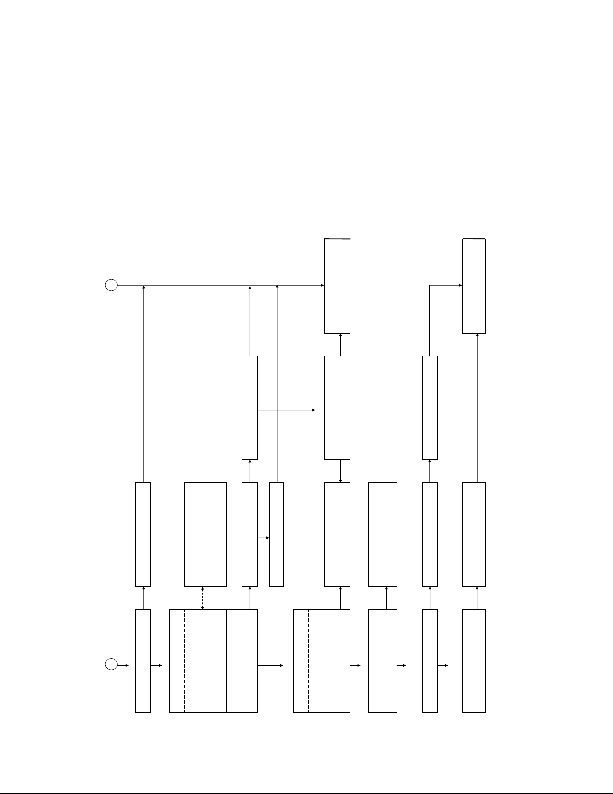
p
p
P
h
k
(
g
)
BDP-BX37/S270 /S370/S37 3/S470
B
No
seY seY seY
soon go "L"
All the ports go "H" within 2 to 10 ms, but
No
Check for shorts at each port
No
No
Do the symptoms improve after checking the
soldering and pattern of IC1503?
Yes
FE_SW5V
SW3.3V and SATA_1.2VA output
CORE_1.1V output
DDR2_1.8V system output
Is there a problem with the mounting
condition of R1512, C1508 or R1515?
No
ort
ut
A
* Corresponding output
ec
Yes
DCSW5V
Yes Replace IC1503 or replace the MB board
SW3.3V Short circuit operation check
is the SW3.3V voltage output?
When IC1503 pin20 PCONT3 has gone "H",
No To Power Supply (System) flowchart No
No Replace IC1503 and the MB board
Yes
No
Do the symptoms improve after replacing
IC101?
No
Is there a problem wit h the mounting
conditon of R1558 or R1562?
No
Yes
Yes
No Replace IC1503 or replace the MB board
R1132, or R1133?
Is there a problem with the mounting
conditon of RB1503, R1543, R1546, R1131,
No
nal check
IFco n Section Flow Cha rt (2/2 )
Check of IFcon reset in
Is the voltage of IC1503 pin6 "H"(3.3V)?
cont output port c
Check of each power supply control port
when the power is ON
IC1503 pin21 PCONT2
IC1503 pin20 PCONT3
IC1503 pin 30 PCONT_CORE
IC1503 pin31 PCONT4
IC1503 pin33 ATA_PCONT
Is the voltage at the "H" level(3.3V)?
Power supply output check
Check the output of the corresponding
voltage
FE_SW5V
1.2VA output
CORE_1.1V output
DCSW5V
DDR2_1.8V output
9-5
Check S Y S_RST signal output
503 pin35 "H"(3.3V)?
are OK
Is IC1
The mounting condition of R1117 and R1156
Do cyclical "H" and "L" communication
CP U (S YSC ON_RE Q signal check)
Che ck the communica tion with the h ost
Serial communication si
PU
Do cyclical "H" and "L" communication
C
waveforms come to IC1503 pin25, 26 and
waveforms come to IC1503 pin36?
27?
Che ck the communication with the host
Page 94
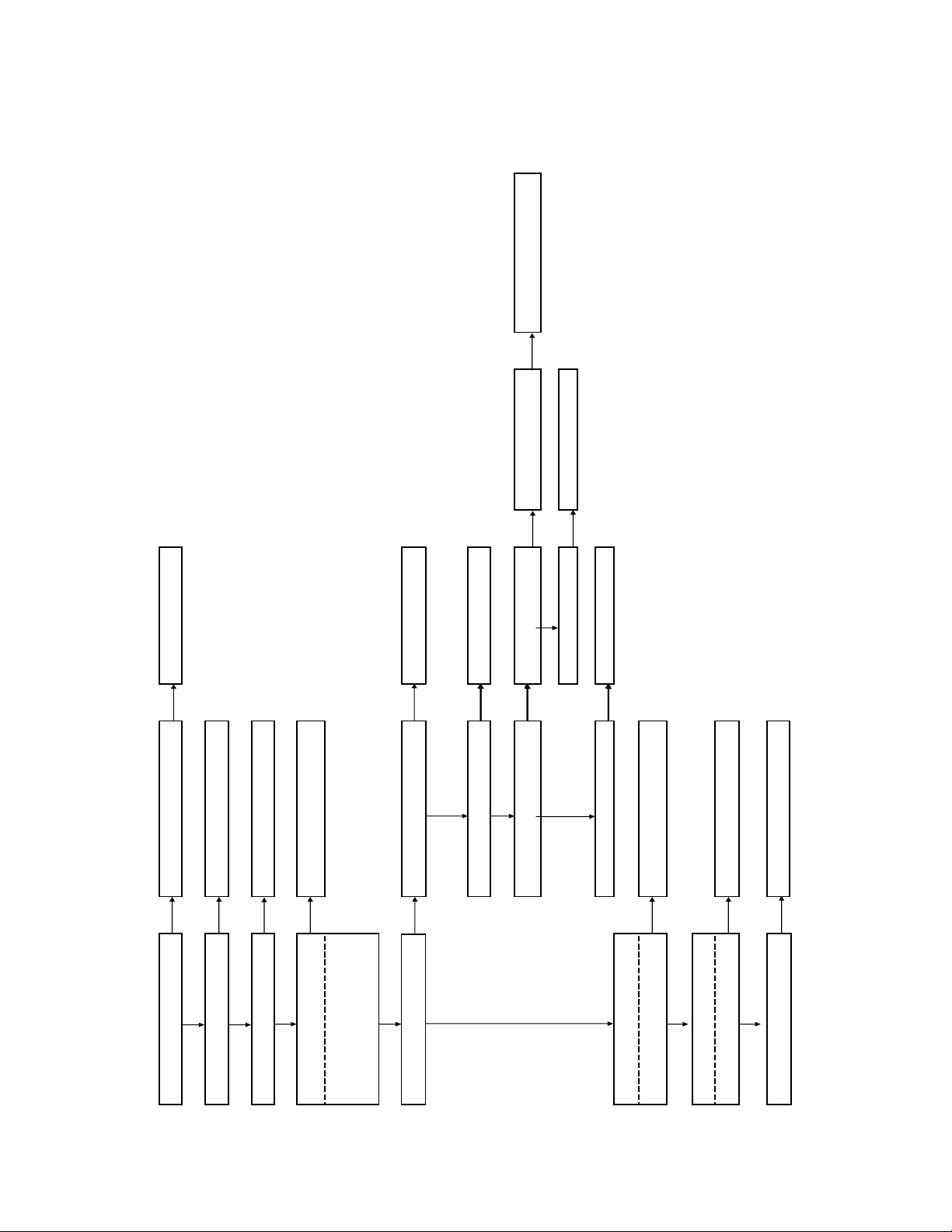
BDP-BX37/S270/S370/S373/S470
No Replace the MB board
with mount
No
No
To Video section flowchart
Video is output properly
No
To Main flowchart
No
To Drive flowchart
No
To Power Supply (System) flowchart
Replace the MB board
No
affected?
No Only Digital Audio (HDMI, Optical, Coax)
Replace the MB board
No
Is there HDMI output?
condition of R991
Is there a problem
Is there Coaxial output? No
No
Is there Optical output?
Yes
Yes Is IC904 lighted up? No Replace IC904
Replace Q909 or replace MB board
No
Is there Coaxial output?
No
Replace the MB board
Replace the MB board
No
Replace IC901 or replace MB board
No
Audio section flowchart
Audio does not sound right
Yes
Yes
Is the FL display/LED display correct?
Is the drive operating properly?
Yes
Is each power supply supplied to the AUDIO
Block?
IC304 pin4: +5V
CN305 pin4: +3.3V
Yes
Yes Yes
Only Analog 2ch L/R Audio affected?
9-6
Is there audio system digital signal input to
IC901?
IC901 pin7: DACDAT
IC901 pin8: LRCK
Yes
Are control signals input to IC901?
C901 pin11: XMUTE
I
Yes
Is there a problem with mount condition of
C910, R962
Page 95
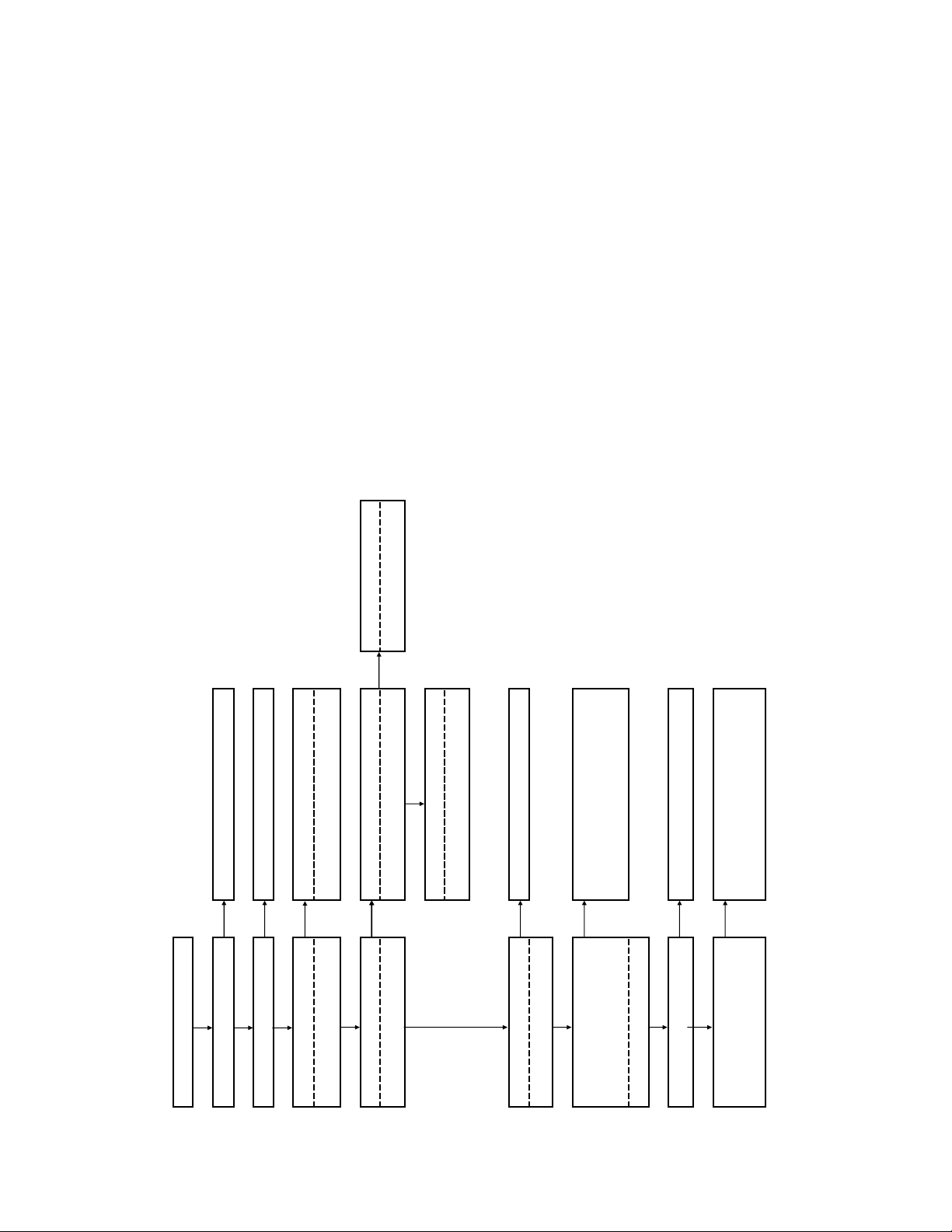
BDP- S270/BX37 /S370/S373/S470
Check the writing fro m IC10 1
No
Yes
R1035)
Replacement device
When IC1001 is defective: Replace IC1001
To Main flowchart
To Drive flowchart
Replace the IC link
When IC1001 is defective: Replace PS302
When IC1002 is defective: Replace PS303
No
No
No
Yes
Yes
Yes
When IC1001 is defective: Check PCONT3
Check the control lines
When IC1002 is defective: Check PCONT2
No
Yes
Yes
When IC1002 is defective: Replace IC10 02
Check the writting from IC101
No
Yes
Check the writting from IC101
No
Yes
(XVMUTE +3.3V)
Replace IC1003
No
Yes
Yes
Check the pin jack block
Check output resistors
(R1031,R1028,R1029,R1030,R1032,R1033,R1034 and
No
Video section flowchart
Reproduced video does not appear right
Is the FL display/LED display correct?
Is the drive operating properly?
Check the input of each power
IC1001 pin 5 :+6V
IC1002 pin 2 :-6V
IC1001 pin 4 :+3V
IC1002 pin 3 :-5V
Check the output of each power
Are video signals input to IC1003
Pin1 CVBS signal
Pin7 Y signal
Are control signals input to IC1003?
Is a video signal output from IC1003?
IC1003 pin8 MUTE
Is a signal output from each Video output
connector?
9-7
Page 96
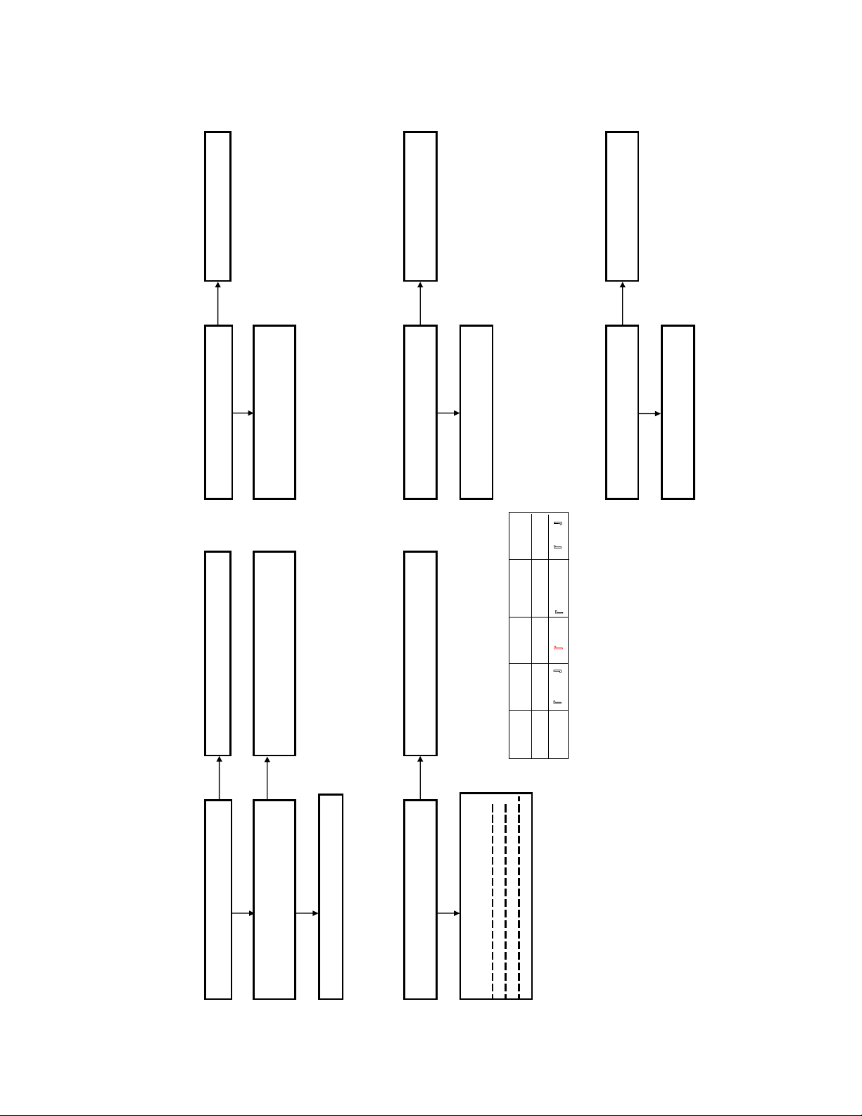
y
p
p
g
y
y
p
y
p
pattern
y
p
pattern
BDP-BX37/S270/S370/S373/S470
To IFcon section flowchart
No
To IFcon section flowchart
No
To IFcon section flowchart
No
s?
the ke
erate
ressin
erate
erate
Yes
1 does not o
Ke
Is there voltage of about 3.3V at pin 2
of CN402 without
Check the resistance of resistors of
Key1 line. Also check the surrounding
pattern.
2 does not o
Is there voltage of about 3.3V at pin 4
of CN402 without pressing the keys?
Check the resistance of resistors of
Key2 line. Also check the surrounding
{KEY3}
Key_OFF
{KEY2}
Key_OFF
{KEY1}
Key_OFF
PLAY
OPEN/CLOSE
STOP
3 does not o
Is there voltage of about 3.3V at pin3
of CN402 without pressing the keys?
Ke
Check the resistance of resistors of
Key3 line. Also check the surrounding
{KEY0}
POWER
Key_OFF
Input
To IFcon section flowchart
No
Check pattern and S331 might be broken
No
Yes Yes
Yes
To IFcon section flowchart
No
Yes Yes
erations cannot be made on the Ke
Reference: Relationship of Buttons and Voltages
0.00-0.40
2.90-3.30
o
SWP/SWB Board flowchart (1/1)
Power button on the main unit does not work
Does symptom improve when replacing the
The potential of pin 2 of CN331 does not
SWP board?
change from 3.3V to near 0V when pressing
the power button
Disconnected harness or replace SWP board
Does symptom improve when replacing the
SWB board?
Ke
Which row of keys do not operate?
PLAY button -> To Key3 does not operate
OPEN/CLOSE button -> To Key2 does not operate
STOP buttons -> To Key1 does not operate
9-8
Page 97
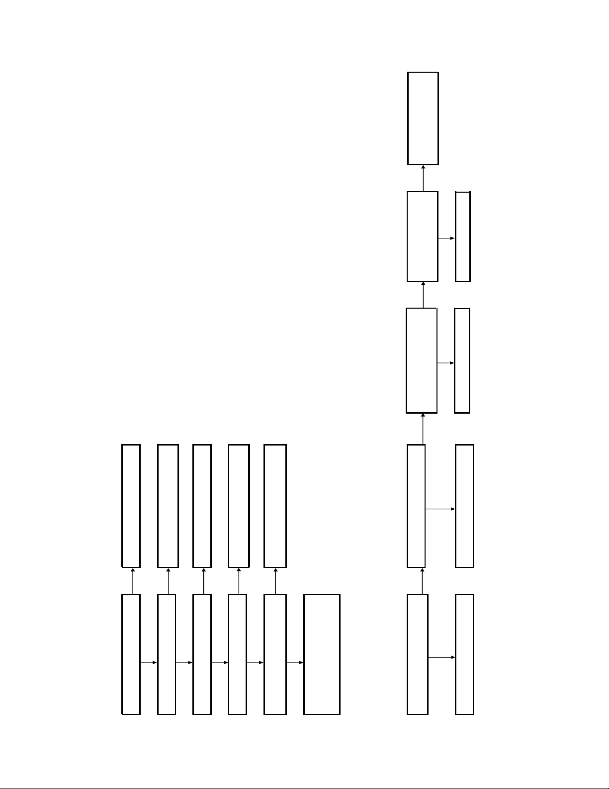
(
)
g
board.
g
BDP-BX37/S270/S370/S373/S470
Replace FFC and Check pattern
Replace IC1503 or MB board if
near IC1503 of MB board.
No
Yes
To FLD Switch Surrounding Check
CONVERTER.
Check the 3.3V line of the FR board.
Replace FFC between FR and MB. If no
effect, then goto IFD flow
Is pin7 of CN702 at 3.3V?
No
Is the voltage of the base of Q703 at
No
Replace the FR board
Yes
3.3V?
Replace Q703
Yes
1/2
FR Board flowchart
ht
FLD does not li
No
Yes
Is there voltage of about 5.8V at PS701?
No Check the circuits surrounging the FLD DD
Is there voltage of about -22V at JL701?
No
Yes
Is there voltage of 3.3V at Pin43 of IC702?
Yes
No Replace IC702. If no effect, replace the FR
Is pin5 of IC702 oscillating?
No
Yes
Yes
Is there input of pulse to pins 7, 8 and 9 of
IC702?
9-9
Check connection of FLD and IC702.
Replace IC702 if OK.
If no defect, replace the FR board
Yes Is the collector voltage of Q703 about 0V?
Check
FLD Switch Surroundin
No
Is the potential of the base of Q704 around
5V?
Replace Q704 Replace Q704
Page 98
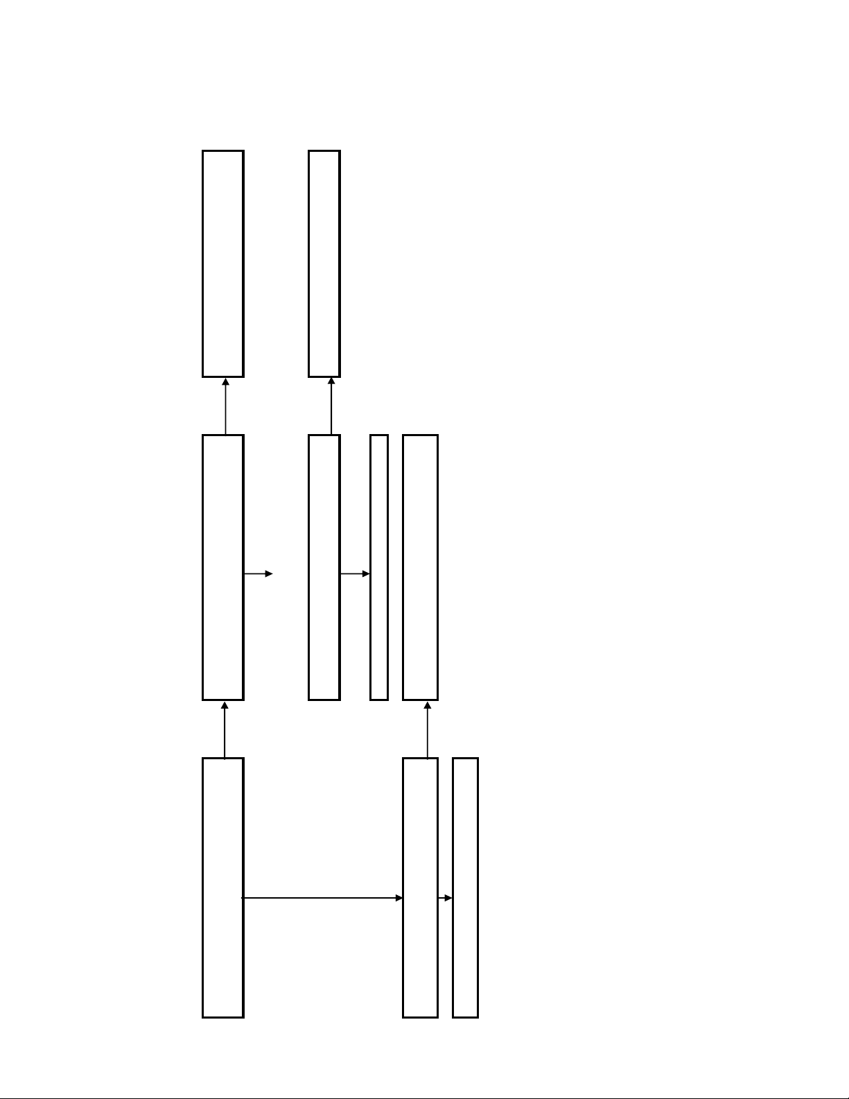
(
)
p
No
BDP-BX37/S270/S370/S373/S470
Replace FFC
Yes
Are there signals to pin13 of MB board
CN1504?
No
erate
2/2
Yes Yes
Are there signals to IC1503 pin24? No Check MB pattern near IC1503
To IFcon section flowchart
Replace IC701 and check FR board pattern
No
Yes
FR Board flowchart
Remote control does not o
Symptom improve when replacing FR
board?
Is there output of about 3.3V for potential of
CN702 pin13?
9-10
Disconnected flexible harness
Page 99
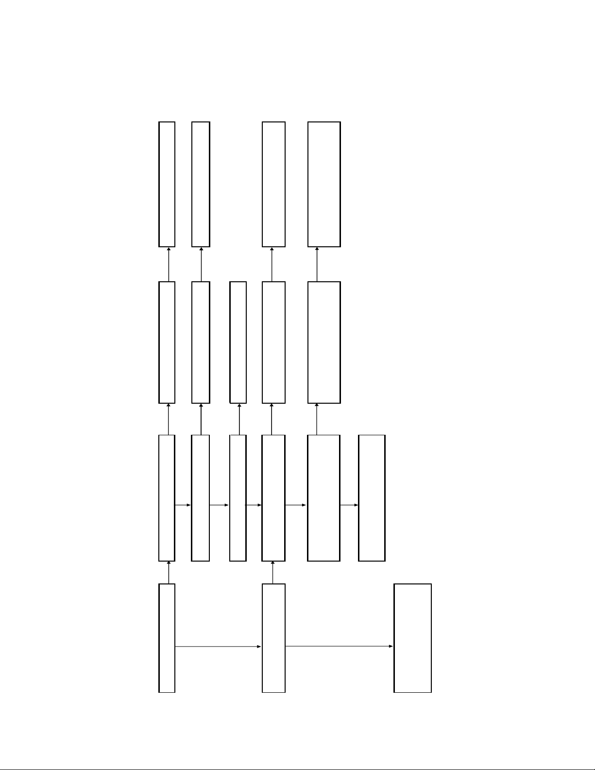
IC1503 or MB Board if NG.
BDP-BX37/S270/S370/S373/S470
Replace MB Board.
No
Symptom improve when replacing FFC?
No
Yes
Check pattern near IC1503 of MB Board. Replace
No
Symptom improve when replacing FR Board?
No
Replace FR Board.
No
Yes
Replace MB Board.
No
Symptom improve when replacing FFC
No
Yes
Yes
Replace IC702. If no effect, replace the FR board.
No
Symptom improve when replacing FR Board?
No
Yes
FR Board flowchart
Is Pin 3 of CN702 at 6V?
No
White LED does not light
Is there voltage of about 5.8V at PS701?
Is the potential of R730 is 6V?
Yes
Symptom improve when replace PS701
Is Pin 6 of CN702 at 3.3V?
No
Is there voltage of about 3.3V at Base
Q709?
Is the potential of R718 is 3.3V?
Yes
Replace R718
Check connection of FLD and IC702.
Replace IC702 if OK.
If no defect, replace the FR board
9-11
Page 100
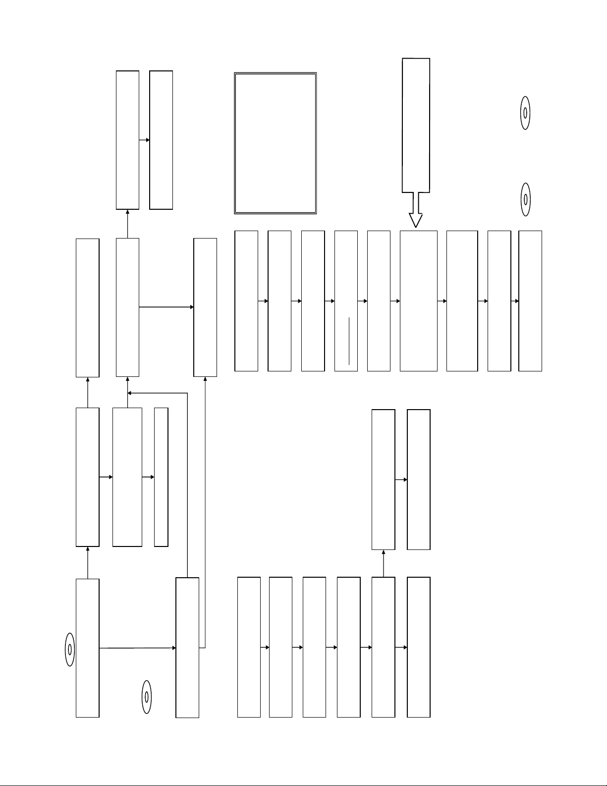
NO
BDP-BX37/S270/S370/S373/S470
DVD: HLX-513
CD: HLX-A1
(Flowchart yy)
BLX-104
Replace the Optical Block Unit (BU)
Optical Block Unit (BU) replace
USB memory
Digital camera (with macro mode)
Barcode decoder (BDBUDec.exe)
installed in jig
ESD free work bench
PC's (jig purpose)
(1) Replace BU (MB is original)
(2) Replace MB (BU is original)
(3) Replace both BU and MB
The following cases need OP Data Write:
JIG requirement
Explanation:
Mode: 1 --> BDP-BX37/S270/S370/S373/S470
Mode: 2 --> BDP-BX57/S570
Check PS301, PS302, PS303
NO
Check Drive Power Supply
NO
Replace PS when open
CN301 Pin 2: 12V / Pin 6: 5V
YES
YES
and save the test data to
BU IOP is OK?
Barcode photo by camer a
service mode. (Flowchart zz)
Check the Optical Block Unit (BU) by
NO
YES
OK
BDP-S370 operates normally
OP FFC cable (1 -837-494-11)
SPDL FFC cable (1-837-495-11)
Check / replace the FFC cable, then check
NO
Optical Block or BU no problem
Remove the defective BU from Loading
Unpack new BU and take OP Data
Assy and also remove BU insulator (4pcs)
Assy (tighten screw with 2kgf)
Assemble BU with Insulators to Loading
BDBUDEC.exe
Decode the OP Data Barcode phot using
memory to USB connector
Enter Service Mode and insert USB
USB memory(File Name: BuData.txt)
replacement
IOP out of specification need BU
NO
Select [8] Drive -->
Press ENTER
Select [2] Mode: 1 or 2
Select [1] Drive OP data Write -->
(Flowchart yy)
Optical Block Unit (BU) replace
--> Turn AC Power OFF
After Finishing ReWrite OP data
Menu to verify IOP in specification
And confirm dIOP by select [7] OP Check
OFF
Turn Power ON and check playback
IOP in specification -- > Turn AC Power
performance using BD, DVD and CD
BLX-104
-
YES
YES
Enter Service Mode
and plug in AC Power
<OPEN/CLOSE>., <PLAY>,<STOP>
BDP-S370 can play the BD-disc
Drive flowchart
DVD: HLX-513
BDP-S370 can play the DVD/CD-disc
CD: HLX-A1
Optical Block Unit (BU ) IOP check flow (zz) ~ [Before BU Replacement] Optical Block Unit (BU ) OP Data Write Flow (yy) ~ [After BU/MB Replacement]
Inside *Service Mode Menu
Press
Inside *Drive
Select [8] Drive
Inside *OP Check Menu
Select [7] OP Check Menu
Select [3] dIOP then press 'ENTER'
+
YES
-
+
BD: 6mA
Specification dIOP
AC Power OFF
DVD, CD: 9mA
l
9-12
 Loading...