

Page 1

Distribution
Restraint
Internal Outside
Prohibited Prohibited
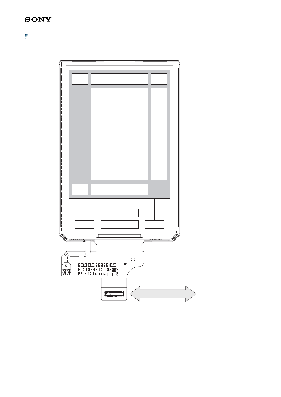
7.96cm 320 480 16,777,216 colors HVGA Transflective color LCD Module
ACX567AKM-7
Description
This display is a 7.96cm diagonal active matrix transflective color LCD module based on Low temperature
polycrystalline silicon TFT technology. This LCD has 320 480 pixels and integrated driver which provides a
symmetric module with narrow edge frame. This module includes a LED backlight and a memory integrated
one chip driver IC with Low power consumption. The driver IC contains FL3G/SPI and RGB interface circuit,
partial memory, CABC function and DC-DC converter.
(Application: Smartphone)
Features
LCD type : Transflective
Symmetric and narrow frame edge module
Dot layout : RGB stripe
Number of dots : 320 RGB 480 / Portrait type
Dot size : 0.046mm 0.138mm (184ppi)
Number of colors : 16,777,216 (R,G, B each 8bit)
Interface : 8bit FL3G/SPI or RGB
Partial RAM size : 320 120 3bit
Supply voltage : VDD_18 1.8V 5%
DD (VBATT) 3.0V 3%
V
Low power consumption : 32mW (max.) (Vertical B/W worst image @VBATT = 3.7V)
100W (max.) (Standby mode)
High reflectivity : 1.7% (@Diffusion)
High contrast ratio : 700:1 (typ.) (LED backlight on)
Luminance (LED backlight on) : 400cd/m
Built-in DC-DC converter
Weight : 15g
2
(typ.)
Prohibited Prohibited
Sony reserves the right to change products and specifications without prior notice. This information does not convey any license
by any implication or otherwise under any patents or other right. Application circuits shown, if any, are typical examples illustrating
the operation of the devices. Sony cannot assume responsibility for any problems arising out of the use of these circuits.
- 1 -
E08Z19-SP
Page 2

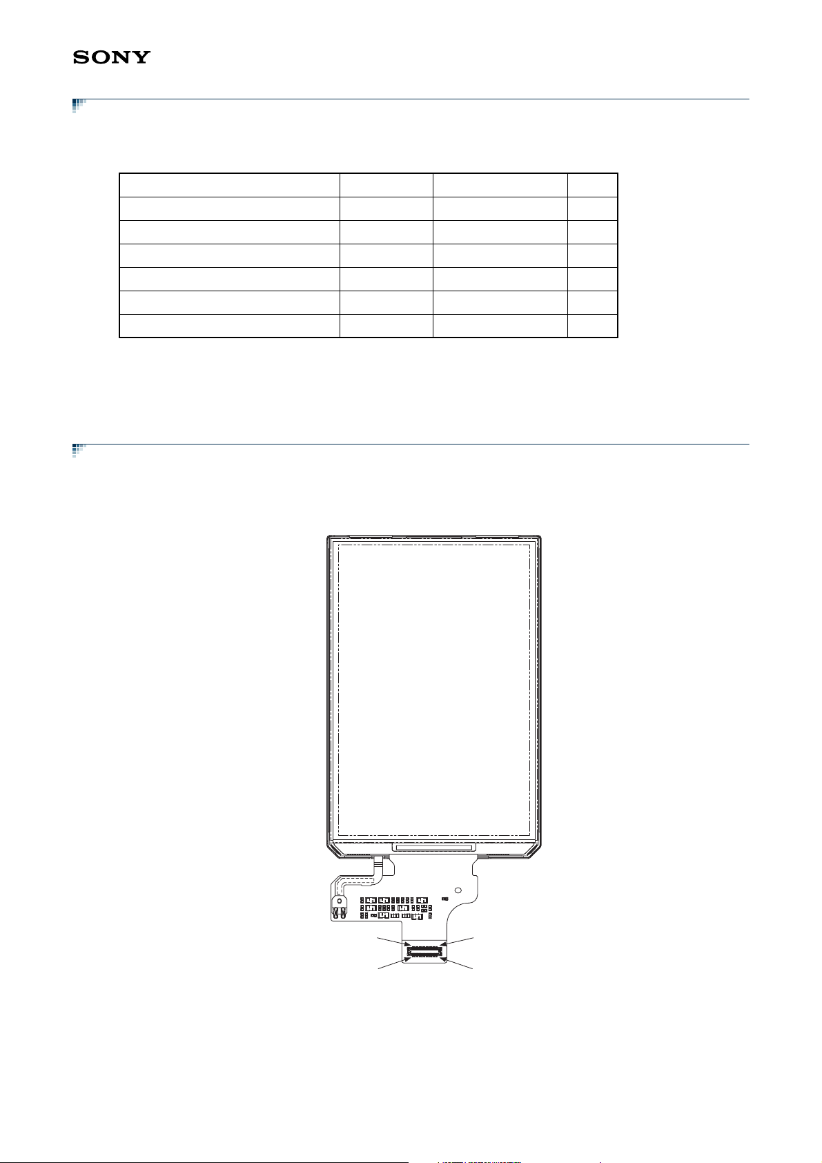
ACX567AKM-7
Element Structure
Active matrix TFT-LCD panel with built-in peripheral driving circuitry using Low temperature polycrystalline
silicon transistors.
Driver IC mounted on TFT glass as COG
5 LEDs backlight
Hardcoated surface polarizer
Number of active dots: 320 (H) 3 480 (V) = 460,800
Dimensions
Module dimensions: 49.86mm (W) 75.19mm (H) 1.64mm (t)
Thickness: from top polarizer to FPC surface
Effective display dimensions (Active area): 44.16mm (H) 66.24mm (V)
- 2 -
Page 3
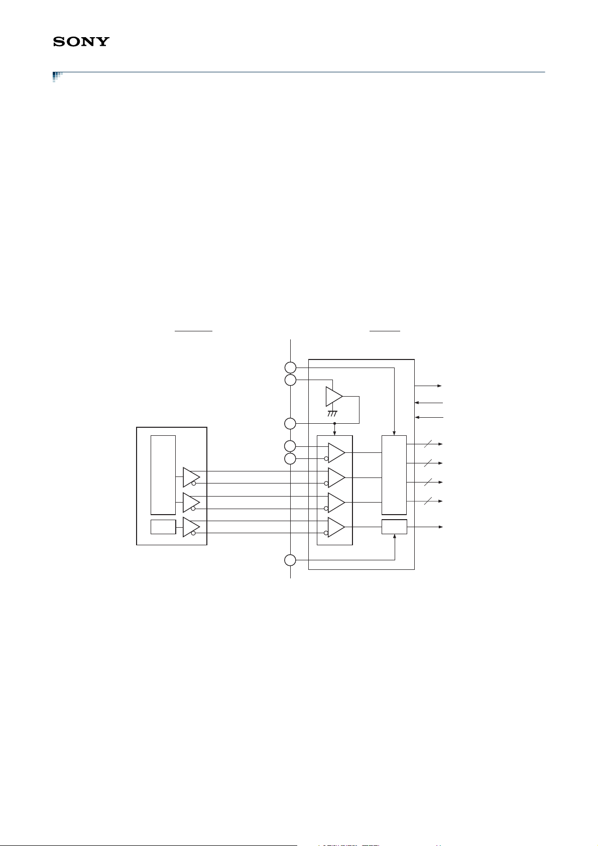
ACX567AKM-7
Block Diagram
The panel block diagram is shown below.
TSW-
control
Precharge/TEST circuit
Active Area
320 × RGB × 480
TSIG-
control
VCS-
Driver
Selector
Control
Selector SW
COG
TEST PAD1 TEST PAD2
I/F PAD
V
DD
VDDIO
RESETX
SPI
CSX
WRX
RDX
SDX
Sub_LVDS
CLK+, CLK–
D0+, D0–
D1+, D1–
B/L
LED_Anode
LED_Cathode
Matching connector:
501591-3010 (Molex)
- 3 -
Page 4
ACX567AKM-7
Absolute Maximum Ratings
(VSS = 0V)
Parameter Symbol Rating Unit
Power supply voltage 1 V
Power supply voltage 2 V
Logic signal input voltage 1 (
Logic signal output voltage (
Operation temperature Topr –10 to +60
Storage temperature Tstr –30 to +70
Note)
Ta = –30 to +70C (no damage at –40 to +85C)
*1
SPI_CS, SPI_DI, SPI_CLK, RESETX
*2
SPI_DO, PWM_LCD
Pin Location
The pin assignment is described in the next page. The location of Pad is shown below.
BATT –0.3 to +5.5 V
DD_18 –0.3 to +3.0 V
*1
)VI1 –0.5 to VDD_18 + 0.5 V
*2
)VO –0.5 to VDD_18 + 0.5 V
C
C
Pin 2
Pin 1
Pin 30
Pin 29
- 4 -
Page 5
ACX567AKM-7
Pin Description
Pin No. Symbol I/O Description
1N.C. Non connect. For customer, this pin should be open.
2BL LED ANODE Common anode for LED's
3BL LED CATHODE Common cathode for LED's
4SPI_CS ISerial interface CHIP SET input
5PWM_LCD OPWM signal output for LCD
6SPI_DI/DO I/OSerial interface DATA input/output
7N.C. Non connect. For customer, this pin should be open.
8GND Ground
9N.C. Non connect. For customer, this pin should be open.
10 GND Ground
11 GND Ground
12 FL3G D0– I Negative polarity signal of High-speed data channel 0
13 SPI_CLK I Serial interface clock input
14 FL3G D0+ I Positive polarity signal of High-speed data channel 0
15 GND Ground
16 GND Ground
17 RESETX I Hard reset input. (Active-Low)
18 FL3G CK– I Negative polarity signal of High-speed clock channel
19 GND Ground
20 FL3G CK+ I Positive polarity signal of High-speed clock channel
21 V
BATT PPositive power supply 3.0V
22 GND Ground
23 VBATT PPositive power supply 3.0V
24 FL3G D1– I Negative polarity signal of High-speed data channel 1
25 V
DD_18 P Positive power supply 1.8V
26 FL3G D1+ I Positive polarity signal of High-speed data channel 1
27 V
DD_18 P Positive power supply 1.8V
28 GND Ground
29 NVM
Non connect. For customer, this pin should be open.
Using SONY's manufactory only.
30 N.C. Non connect. For customer, this pin should be open.
- 5 -
Page 6
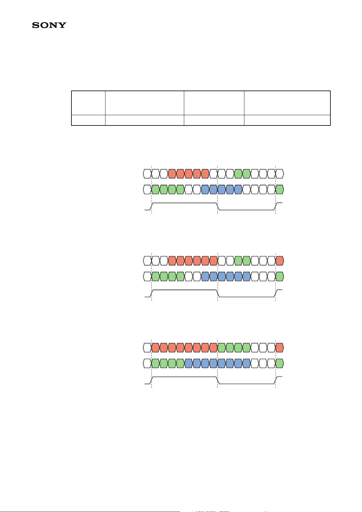
Color Table
ACX567AKM-7
Color & gray
scale
Gray scale
level
R0 R1 R2 R3 R4 R5 R6 R7 G0 G1 G2 G3 G4 G5 G6 G7 B0 B1 B2 B3 B4 B5 B6 B7
Data signal
Black — L L L L L L L L L L L L L L L L L L L L L L L L
Blue — L L L L L L L L L L L L L L L L H H H H H H H H
Green — L L L L L L L L H H H H H H H H L L L L L L L L
Cyan — L L L L L L L L H H H H H H H H H H H H H H H H
Red — H H H H H H H H L L L L L L L L L L L L L L L L
Magenta — H H H H H H H H L L L L L L L L H H H H H H H H
Yellow — H H H H H H H H H H H H H H H H L L LLLLLL
White — H H H H H H H H H H H H H H H H H H H H H H H H
Black GS0 L L L L L L L L L L L L L L L L L L L L L L L L
GS1 H L L L L L L L L L L L L L L L L L L L L L L L
Darker GS2 L H L L L L L L L L L L L L L L L L L L L L L L
—
—
Brighter GS253 H L H H H H H H L L L L L L L L L L L L L L L L
GS254 L H H H H H H H L L L L L L L L L L L L L L L L
Red GS255 H H H H H H H H L L L L L L L L L L L L L L L L
Black GS0 L L L L L L L L L L L L L L L L L L L L L L L L
GS1 L L L L L L L L H L L L L L L L L L L L L L L L
Darker GS2 L L L L L L L L L H L L L L L L L L L L L L L L
—
—
Brighter GS253 L L L L L L L L H L H H H H H H L L L L L L L L
GS254 L L L L L L L L L H H H H H H H L L L L L L L L
Green GS255 L L L L L L L L H H H H H H H H L L L L L L L L
Black GS0 L L L L L L L L L L L L L L L L L L L L L L L L
GS1 L L L L L L L L L L L L L L L L H L L L L L L L
Darker GS2 L L L L L L L L L L L L L L L L L H L L L L L L
—
—
Brighter GS253 L L L L L L L L L L L L L L L L H L H H H H H H
GS254 L L L L L L L L L L L L L L L L L H H H H H H H
Blue GS255 L L L L L L L L L L L L L L L L H H H H H H H H
- 6 -
Page 7
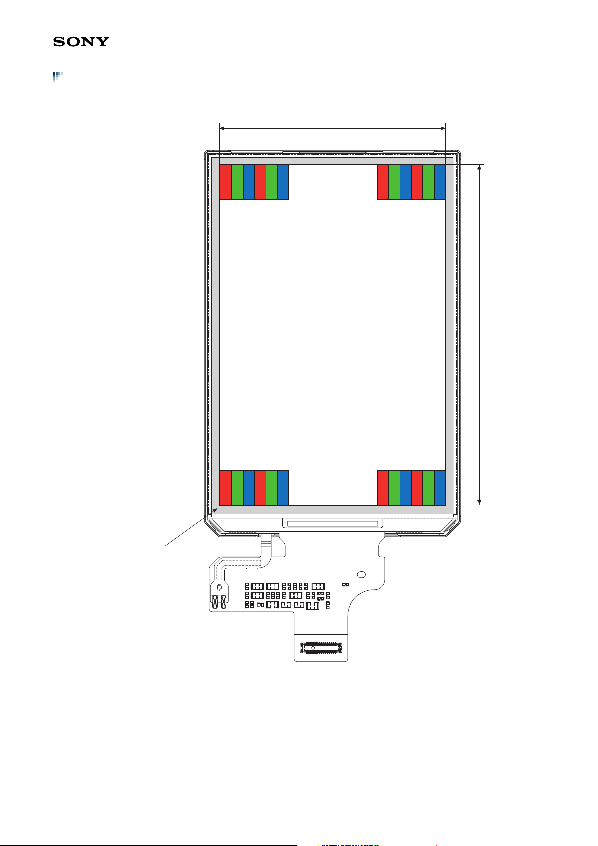
Color Coding
ACX567AKM-7
Active Area: 320 pixels
RGBRGB RGBRGB
Black Mask
Active Area: 480 pixels
RGBRGB RGBRGB
- 7 -
Page 8
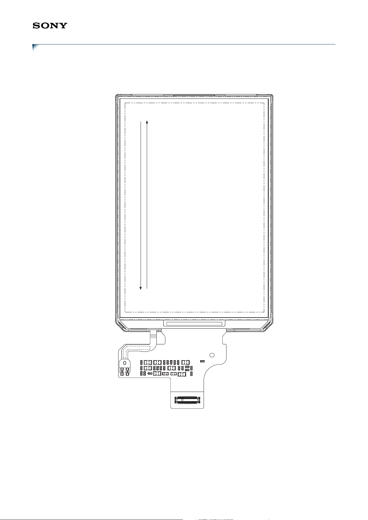
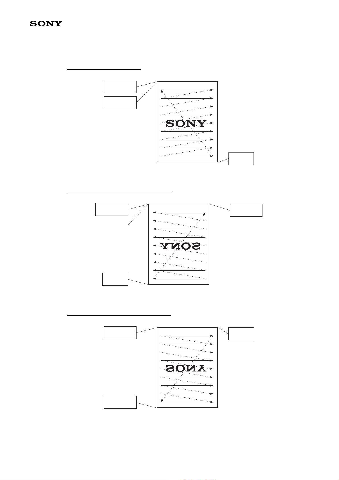
Scanning Direction
The scanning direction for the vertical period are A as shown below.
This scanning directions is from a front view.
ACX567AKM-7
Active Area
320 × RGB × 480
Vertical Direction (DWN = L)
Vertical Direction (DWN = H)
- 8 -
Page 9
ACX567AKM-7
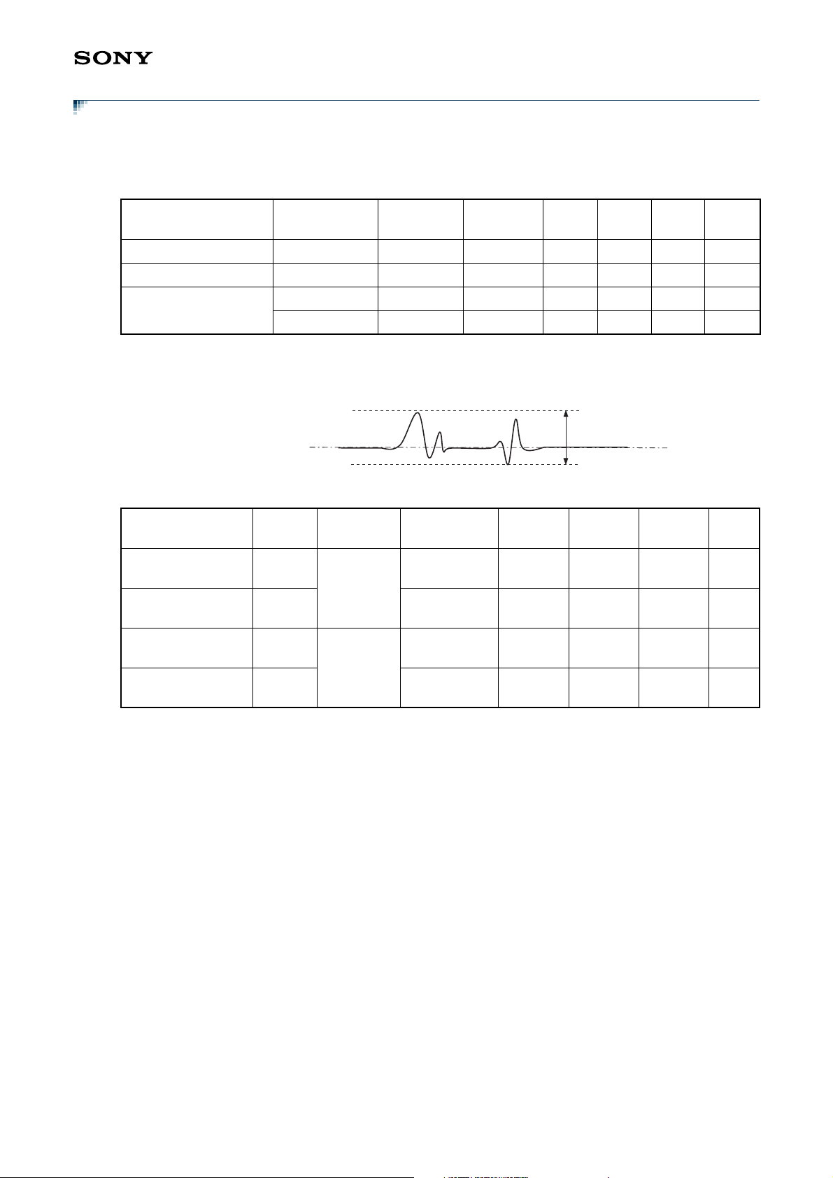
Electrical Characteristics
DC Characteristics
(VBATT = 3.0V 3%, VDD_18 = 1.8V 5%, Ta = –30 to +70C (no damage at –40 to +85C))
Item Symbol
Application
pins
Condition Min. Typ. Max. Unit
Power supply voltage 1 VBATT VBATT –3% 3.0 3% V
Power supply voltage 2 V
Power supply voltage
noise
*1
This value is not symmetric amplitude which center point is VDD_18. The value of VDD_18 is an average
DD_18 VDD_18 –5% 1.80 5% V
DD_NOISE VDD_18
V
V
BATT_NOISE VBATT ——300mVp-p
*1
——100mVp-p
value. See example below. These values are valid up to 100MHz.
DD_18 (average)
V
BATT = 3.0V 3%, VDD_18 = 1.8V 5%, Ta = –30 to +70
(V
Item Symbol
Logic High level
input voltage 1
Logic Low level
input voltage 1
Logic OUT High
level output voltage
V
IH1
V
IL1 VSS —
V
DOH
Application
pins
SPI_CS,
SPI_DI,
SPI_CLK,
RESETX,
Condition Min. Typ. Max. Unit
OUT = –1mA
I
C (no damage at –40 to +85C))
0.7
DD_18
V
0.8
VDD_18
100mVp-p
—VDD_18 V
—VDD_18 V
PWM_LCD
Logic OUT Low
level output voltage
V
DOL IOUT = +1mA VSS —
0.3
VDD_18
0.2
DD_18
V
V
V
- 9 -
Page 10
ACX567AKM-7
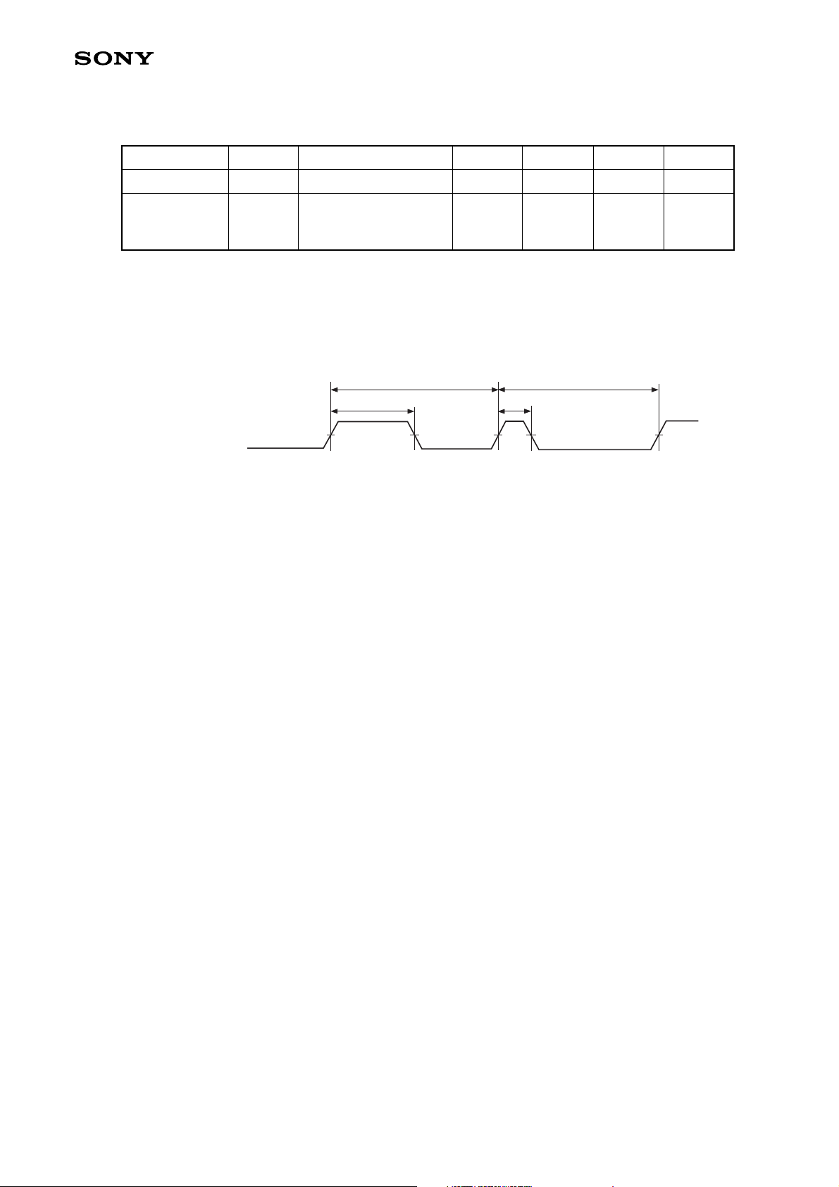
PWM Outputs
(VBATT = 3.0V 3%, VDD_18 = 1.8V 5%, Ta = –30 to +70C (no damage at –40 to +85C))
Item Symbol Condition Min. Typ. Max. Unit
500 Hz
LBV[7:0] = 00h to FFh
PWM_LBL duty d
lpwm
No Load
0—100%
Note2
Note 1: The PWM frequency for LCD B/L is adjustable by internal 8bits register that is programmed to NVM in
Sony’s factory.
Note 2: User can adjust PWM Duty for LCD B/L by register (WRLBV / 51h).
PWM Output for LCD
PWM_LBL
50%
tlcyc
A
50%
dlpwm = A/tlcyc
A'
50%
tlcyc
- 10 -
Page 11
Input Timing
FlatLink3G Interface
ACX567AKM-7
Introduction
The number of data channels between TX and RX is programmable from 1 to 2 depending on bandwidth
needed. The data link speed is defined according to pixel clock (PCLK) of RGB I/F and the number of data
channels. FlatLink3G has 2 different power modes; shutdown and active. In shutdown mode, FlatLink3G
is totally inactive and assumed to consume least power (order of A). In active mode, FlatLink3G works as
a High-speed data link as defined.
TX adds odd parity bit in every data frame and RX checks the pixel data according to the sent parity.
System Block Diagram and Link Protocol
System Block Diagram of FlatLink3G
FlatLink3G consists of three parts; TX, RX and High-speed signaling channels, as shown below.
SET Side
Receiver Block (RX)
VDDI
V
DD
V3G_LDO
D1+/D1–
converter
Parallel to serial
PLL
DDI is a link power and logic level supply and GND is a ground level of all circuits from a system power
V
D0+/D0–
CLK+/CLK1–
V
DD
_PLL
IC Side
PLL
To Internal Circuit
8
8
8
converter
Serial to parallel
3
RX_CPO
RX_LS
RX_SD
RX_R[7:0]
RX_G[7:0]
RX_B[7:0]
RX_HS, VS, DE
RX_PCLK
supply.
TX_R[7:0], TX_G[7:0], TX_B[7:0], TX_VS, TX_HS, TX_DE and TX_PCLK are RGB I/F parallel CMOS
signals provided for TX. PLL of TX provides necessary multiplied clock internally based on TX_PCLK.
TX serializes TX_R[7:0], TX_G[7:0], TX_B[7:0], TX_VS, TX_HS and TX_DE into High-speed data
channels, D0+/D0–, D1+/D1–, D2+/D2–, based on the multiplied clock. TX transfers TX_PLCK into a
High-speed clock channel, CLK+/CLK–, with its original rate. The number of data channels is
programmed by TX_LS and RX_LS.
PLL of RX provides necessary multiplied clock internally based on the High-speed clock channel
inputs. RX desterilizes the High-speed data channel inputs into RX_R[7:0], RX_G[7:0], RX_B[7:0],
RX_VS, RX_HS and RX_DE based on the multiplied clock. TX transfers the High-speed clock channel
into RX_PCLK. RX_R[7:0], RX_G[7:0], RX_B[7:0], RX_VS, RX_HS, RX_DE and RX_PCLK construct
RGB I/F parallel CMOS signals as output.
RX_XSD are CMOS signals for shutdown of TX and RX.
- 11 -
Page 12
ACX567AKM-7
Link Programmability
The number of High-speed data channels is programmed in NVM by CM[2:0].
Table 1 shows the relation among CM, the number of High-speed data channels, the supported
RX_PCLK range and the guaranteed data bandwidth per channel.
Table 1. Link programmability
CM[2:0]
The number of High-speed
data channels
Supported
RX_PCLK range
[MHz]
Supported guaranteed data
bandwidth per channel
[Mbits/sec]
(0, 0, 1) 2 8.0 - 30.0 120 - 450
Option 1: The number of High-speed data channels is 2;
D0 Channel
D1 Channel
CLK Channel (∗)
D0 Channel
CP
res
CP
R4 R3
G0
G2 G1
G3
Protocol for 2-channel deta (16-bit Mode)
R5
R4 R3
R2
B4 B3
R0
R1
R0
R2 R1
B2 B1
G5
B0
G5
G4
G4
VS
HS
VS
res
DE
res
CP
res
CP
G3
R7
D1 Channel
CLK Channel (∗)
D0 Channel
D1 Channel
CLK Channel (∗)
res
CP
res
G3
R7 R6
G3
G0
G0
G2 G1
Protocol for 2-channel deta (18-bit Mode)
R5
R4 R3
G0
G2
G1
Protocol for 2-channel deta (24-bit Mode)
R2
B7 B6
B5
R1
B5
B4 B3
R0
B4 B3
G7
B2
G6
B2
B1
G5
B1
B0
G4
B0
HS
VS
HS
DE
res
DE
res
CP
res
G3
R7
G3
- 12 -
Page 13
ACX567AKM-7
Two Data Channel Case
Item Symbol Condition Min. Typ. Max. Unit
Pixel clock frequency PCLK 8.0 — 30.0 MHz
Pixel clock cycle t
Clock-to-clock
position jitter
Clock-to-data
posittion jitter
CLK Ideal tCLK 60 — 125 ns
t
CLKjitter 0—300ps
t
DATAjitter 0—330ps
Ideal tpos0 position tpos0 Note 2 0 0 0 ns
Ideal tpos1 position tpos1 Note 2 (1/15) tCLK (1/15) tCLK (1/15) tCLK ns
Ideal tpos2 position tpos2 Note 2 (2/15) t
Ideal tpos3 position tpos3 Note 2 (3/15) t
CLK (2/15) tCLK (2/15) tCLK ns
CLK (3/15) tCLK (3/15) tCLK ns
Ideal tpos4 position tpos4 Note 2 (4/15) t
Ideal tpos5 position tpos5 Note 2 (5/15) t
Ideal tpos6 position tpos6 Note 2 (6/15) t
Ideal tpos7 position tpos7 Note 2 (7/15) t
Ideal tpos8 position tpos8 Note 2 (8/15) t
Ideal tpos9 position tpos9 Note 2 (9/15) t
Ideal tpos10 position tpos10 Note 2 (10/15) t
Ideal tpos11 position tpos11 Note 2 (11/15) t
Ideal tpos12 position tpos12 Note 2 (12/15) t
Ideal tpos13 position tpos13 Note 2 (13/15) t
Ideal tpos14 position tpos14 Note 2 (14/15) t
CLK (4/15) tCLK (4/15) tCLK ns
CLK (5/15) tCLK (5/15) tCLK ns
CLK (6/15) tCLK (6/15) tCLK ns
CLK (7/15) tCLK (7/15) tCLK ns
CLK (8/15) tCLK (8/15) tCLK ns
CLK (9/15) tCLK (9/15) tCLK ns
CLK (10/15) tCLK (10/15) tCLK ns
CLK (11/15) tCLK (11/15) tCLK ns
CLK (12/15) tCLK (12/15) tCLK ns
CLK (13/15) tCLK (13/15) tCLK ns
CLK (14/15) tCLK (14/15) tCLK ns
Note 1: Ta = –30 to +70C (to +85C no damage), VDDI = 1.65 to 1.95V, VSS (DGND) = 0V
Note 2: The reference point is when the CLK channel is changing from logical “0” to logical “1” at the 50%
level. This reference point is used to defined ideal t
POSn (n = 0, 1, 2, 3, ... ,14) positions.
- 13 -
Page 14
One Pixel
t
CLK
ACX567AKM-7
CLK Channel
D0 Channel
D1 Channel
Differential CLK
VS
HS
Res
DE
CLK+
D18
5
D17 D16 D15
D6
D5 D4
t
POS
tPOS
6
tPOS
7
8
D19
D7
4
t
POS
tPOS
D23
CP
Res
D11
0
t
POS
D21
D22
D10
POS
t
1
D20
D9
D8
POS
t
2
3
tPOS
Data Position - Two Data Channel Case
CLK_jitter
t
tCLK_jitter
CLK–
D13
D1
POS
t
11
D12
D0
POS
t
12
D14
D3
D2
POS
t
9
tPOS
10
HS
tPOS
13
Res
DE
t
POS
14
CP
Res
D23
D11
VS
D22
D10
D21
D9
50%
0
Differential Data
50%
50%
50%
tDATA_jitter
tDATA_jitter
Ideal Data Position
(tPOSn) n = 0, 1, 2..., 14
Clock and Data Jitters - Two Data Channel Case
0
- 14 -
Page 15
DC Characteristics for FlatLink3G
Module
ACX567AKM-7
IC
V3G_LDO
SS_LVS
V
Vdiff_rx
InP
Rinp
R_rx
InN
Rinn
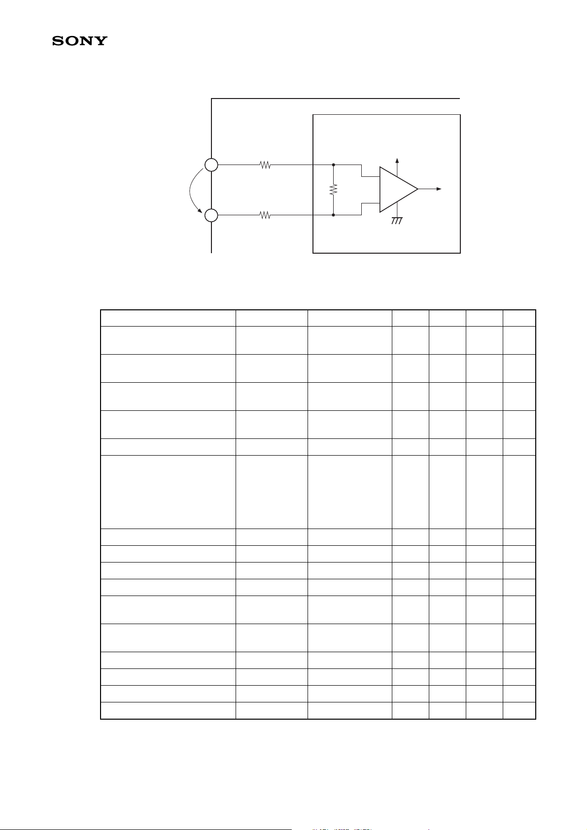
SubLVDS Receiver
SubLVDS Receiver Electrical Characteristics
Item Symbol Condition Min. Typ. Max. Unit
Input differential voltage range
*1
Input Low level threshold
voltage
*1
Input High level threshold
voltage
*1
Input common mode voltage
*1
range
Common mode ripple
*1
Vdiff_rx 70 — 200
mVp-p
VTHL –40 — — mV
VTHH — — 40 mV
Vcm_rx 0.6 0.9 1.2 V
Vcm_rx_ripple –75 — 75 mV
Rinp: 2 (min),
3 (typ),
Differential termination
resistor
R_rx
7.5 (max)
Rinn: 2 (min),
80 100 120
3 (typ),
7.5 (max)
Self bias resistor R_self — — 500 k
*1
Vdiff_rx rise time (20-80%)
Vdiff_rx fall time (20-80%)
tr — — 800 ps
*1
tf — — 800 ps
Operating frequency — — 225 MHz
Amplitude mismatch
(Vdiff _tx/Vdiff_tx)
*2
Common mode mismatch
(Vcm _tx)
Rise time difference
Fall time difference
*3
*4
*4
–10 — 10 %
–0.1 — 0.1 V
–100 — 100 ps
–100 — 100 ps
Input leakage current +/– IIN+/– — — 90 A
Output leakage current +/– IOUT+/– Note — — 3.0 A
Note)
This current is what the host can supply when its differential outputs are in Hi-Z state.
- 15 -
Page 16
ACX567AKM-7
*1
Single-ended
InP
Vcm_rx
Vdiff_rx
0
0
InN
VTHH
Differential (Inp – InN)
tf
20%
60%
20%
Differential (Inp – InN)
VTHL
Vcm_rx_ripple
tr
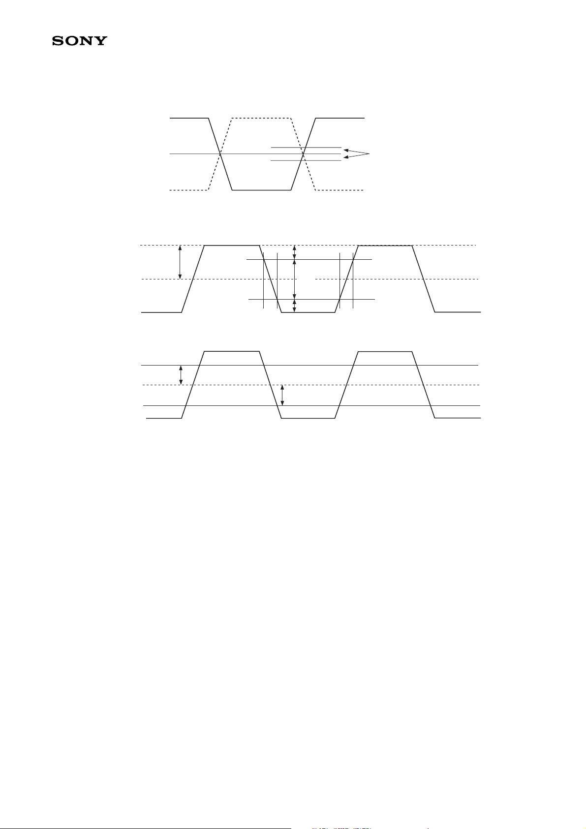
Mismatch is Signal Properties at TX Output Causes Same Mismatches to RX Input
- 16 -
Page 17
*2
Vdiff_tx = Vdiff_CLK – Vdiff_DATA
*3
Vcm_tx = Vcm_CLK – Vcm_DATA
CLKP
ACX567AKM-7
Receiver
CLK:
VDD
Vdiff_CLK
R_rx
CLKN
DATA:
D0/D1/D2
DATAP
Vdiff_DATA
*4
Rise time difference = tr1 – tr2, Fall time difference = tf1 – tf2
R_rx
DATAN
CLK
Vdiff_CLK
tf1
20%
Out_CLK
GND
VDD
Out_DATA
GND
tr1
0
Vdiff_DATA
0
60%
20%
DATA (D0/D1/D2)
tf2
20%
60%
20%
- 17 -
tr2
Page 18
ACX567AKM-7
The FlatLink3G receiver is understanding that there is logical “1” when a differential voltage is more than
VTHH and the FlatLink3G receiver is understanding that there is logical “0” when a differential voltage is
more than VTHH. There is undefined state if the differential voltage is less than VTHH and less than VTHH.
A reference figure is below.
Vdiff_rx
0V Reference
for
Differential Inputs
Vdiff_rx
"1"
"0"
"Undefined"
"1""Undefined"
VTHH
CLK+/–, D1+/–, D0+/–
VTHL
Differential Inputs Logical “0”s and “1”s, Threshold High/Low, Differential Voltage Range
The FlatLink3G transmitter can be driven to Hi-Z on the host side, when the FlatLink3G interface is not used.
Therefore, there is implemented pull-down or pull-up resistor(s) (RSELFBIAS) to avoid e.g. unstable
situations for differential inputs of the FlatLink3G receiver.
Therefore, those two examples, which are shown below, are only for reference purposes, when there is
defined an implementation of the pull-up or pull-down resistor(s) (RSELFBIAS).
V3G_LDO
(R_rx)/2
+
(R_rx)/2
Note)
1. R_self is used if a transmitter is not driven Clock (CLK+/–) or Data (D1+/–, D0+/–) channels.
R_self
–
V
SS_LVS
2. R_self can be implemented as pull-up or pull-down.
- 18 -
Page 19

RGB Interface
General Timing Diagram
ACX567AKM-7
VS
Blanking area (Timing information
that is not possible to see on display)
DE = 0 (Low)
Active area (Image which can
be seen on display)
DE = 1 (High)
HS
Note)
The horizontal and vertical blanking number (also sync widths,
front and back poach number) are unsettled value in this system,
therefore internal synchronization is operated by only DE pulse,
HS and VS are only used reset for H system and V system.
General Timing Diagram
The image information must be correct on the display, when the timings are in range on the interface.
However, the image information can be incorrect on the display, when timings are out of the range on the
interface (Out of the range timings cannot cause any damage on the display module or it cannot cause any
damage on the host side). The correct image information must be displayed automatically (by the display
module) on the next frame (vertical sync.), when there is returned from out of the range to in range interface
timings.
- 19 -
Page 20
ACX567AKM-7
Updating Order on Display Active Area (Normal Display Mode On + Sleep Out)
There is defined different kind of updating orders for Display. These updating orders are controlled by bits.
Normal Scan Direction Mode
Physical point
(0, 0)
Start point
(0, 0)
Updating order when MADCTL's B7 = 0 and B6 = 0
Active area of LCD
Vertical counter (0 - 479)
Horizontal counter (0 - 319)
Left/Right Inversion Scan Direction Mode
Physical point
(0, 0)
Active area of LCD
End point
(319, 479)
Start point
(0, 0)
Vertical counter (0 - 479)
End point
(319, 479)
Horizontal counter (0 - 319)
Updating order when MADCTL's B7 = 0 and B6 = 1
Up/Down Inversion Scan Direction Mode
Physical point
(0, 0)
Vertical counter (0 - 479)
Start point
(0, 0)
Horizontal counter (0 - 319)
Updating order when MADCTL's B7 = 1 and B6 = 0
Active area of LCD
End point
(319, 479)
- 20 -
Page 21
Up/Down and Left/Right Inversion Scan Direction Mode
ACX567AKM-7
Physical point
(0, 0)
End point
(319, 479)
Updating order when MADCTL's B7 = 1 and B6 = 1
Active area of LCD
Vertical counter (0 - 479)
Start point
(0, 0)
Horizontal counter (0 - 319)
Rules for Updating the Display
Condition Horizontal counter Vertical counter
An active VS signal is received Return to 0 Return to 0
Single pixel information of active area is received Increment by 1 No change
An active HS signal is received after a falling edge of DE signal Return to 0 Increment by 1
Rules for Updating Order
Condition Horizontal counter Vertical counter
An active VS signal is received Return to 0 Return to 0
Single pixel information of the active area is received Increment by 1 No change
An active HS signal between two active area lines Return to 0 Increment by 1
The Horizontal counter value is larger than 319 and the vertical
counter value is larger than 479 (In case of 320 480 mode)
Note)
1. Pixel order is RGB on the display.
Return to 0 Return to 0
2. Data streaming direction from the host to the display is described in the following figure.
B
E
Data stream from
Video I/F is
like in this figure.
Data streaming order from RGB I/F
- 21 -
Page 22
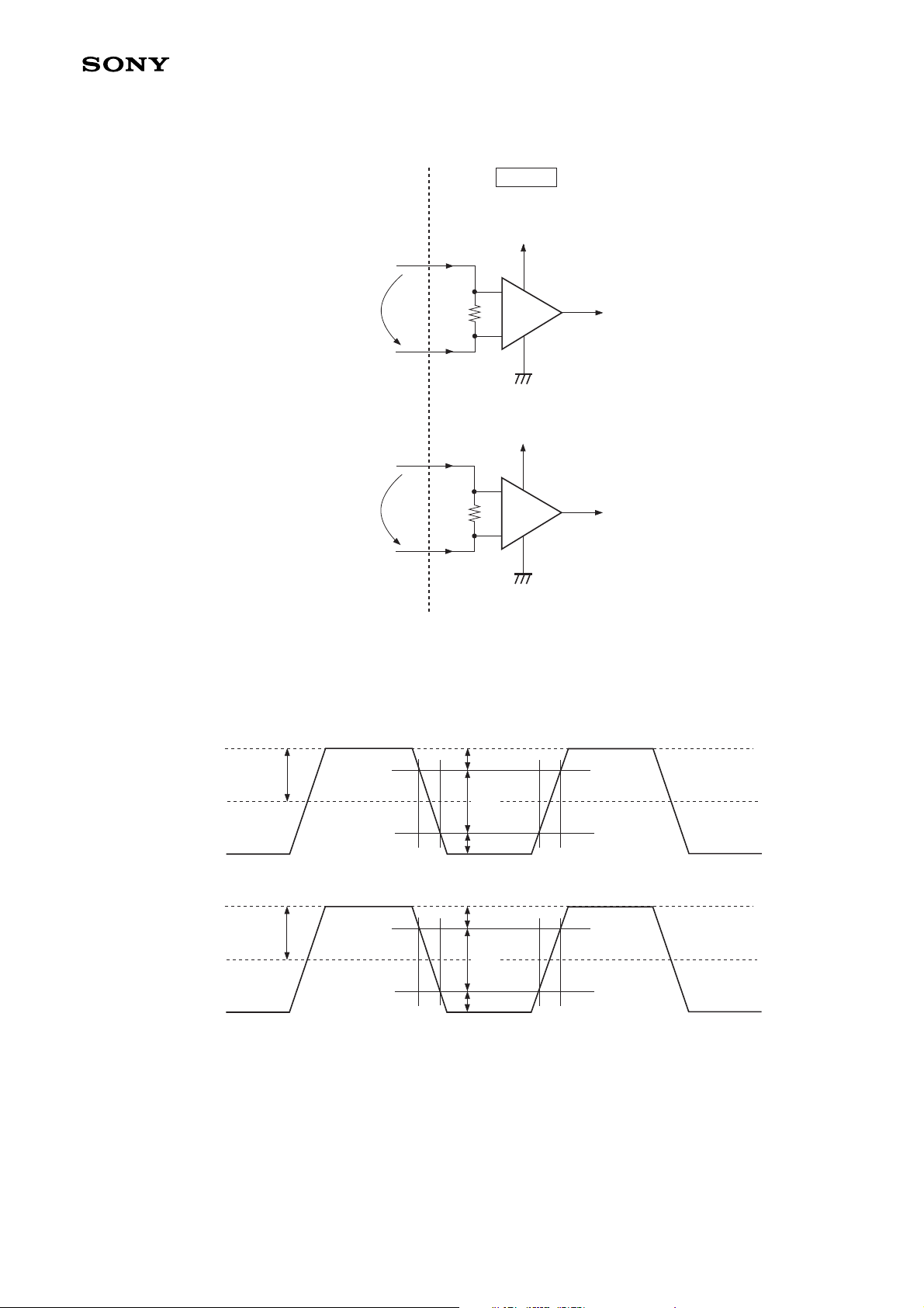
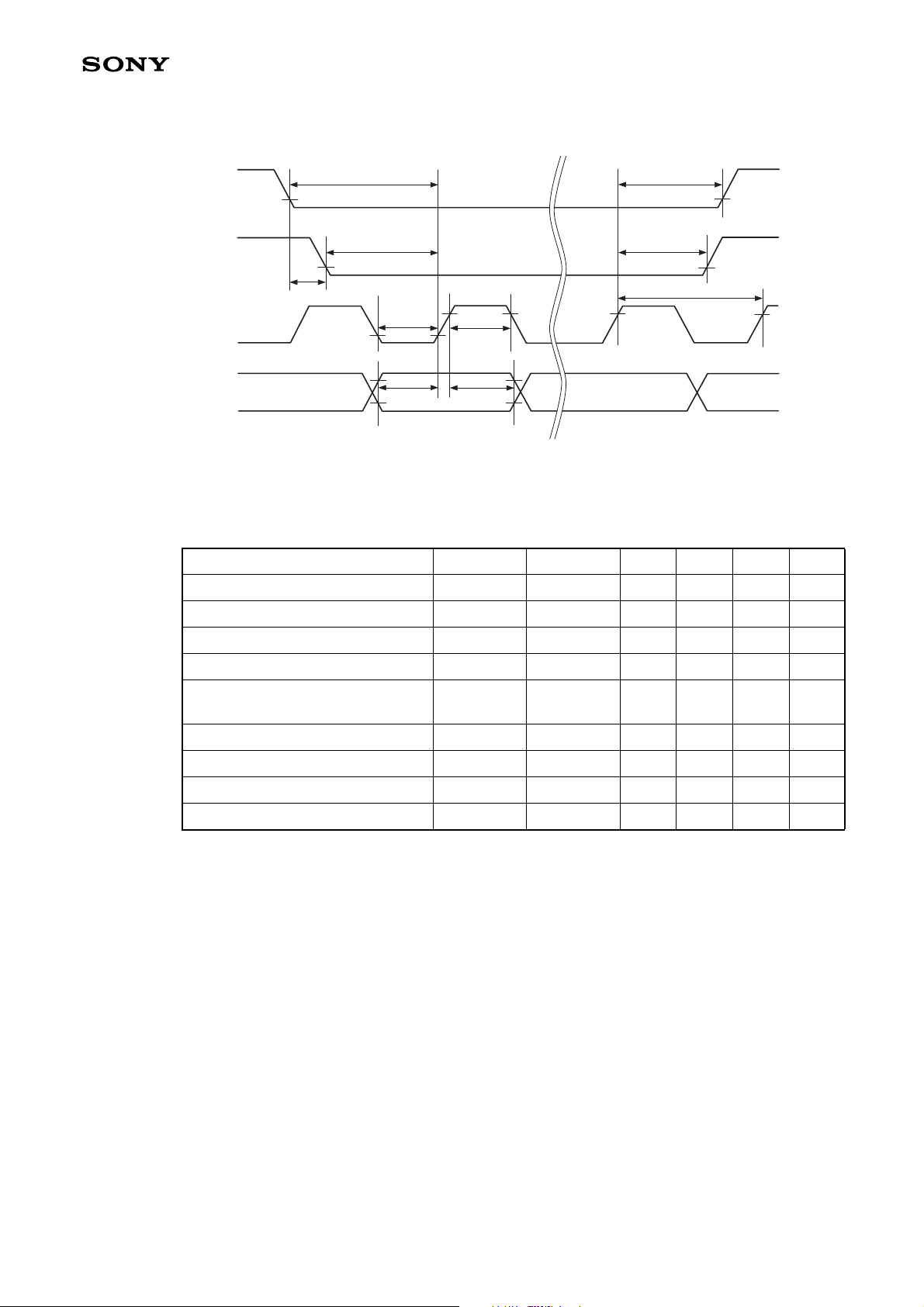
Vertical Timing of RGB Interface (RGB I/F / FlatLink3G)
ACX567AKM-7
VS
Data
DE
HS
VFP
VSW
VBL
VBP
VDISP
VP
Vertical Timing Diagram of RGB Interface (RGB I/F)
Vertical Timing of RGB Interface (320 480 Mode)
(Ta = –30 to +70C, VDDI = 1.65 to 1.95V, VDD = 2.3 to 4.3V, VSS = 0V)
480 Mode
320
Item Symbol Condition Min. Typ. Max. Unit
Vertical cycle VP Normal Mode 486 488 490 lines
Vertical Low pulse width VSW Normal Mode 2 2 4 lines
Vertical front porch VFP Normal Mode 2 3 4 lines
Vertical back porch VBP Normal Mode 2 3 4 lines
Vertical blanking period VBL Normal Mode 6 8 10 lines
Vertical active area VDSIP Normal Mode — 480 — lines
Vertical frequency Normal Mode 50 60 65 Hz
Note)
1. Signal rise and fall times are equal or less than 20ns.
2. Measuring of input signals are using 0.30 V
DDI for Low state and 0.70 VDDI for High state.
3. Data lines can be set to “High” or “Low” during blanking time — Don’t care.
- 22 -
Page 23
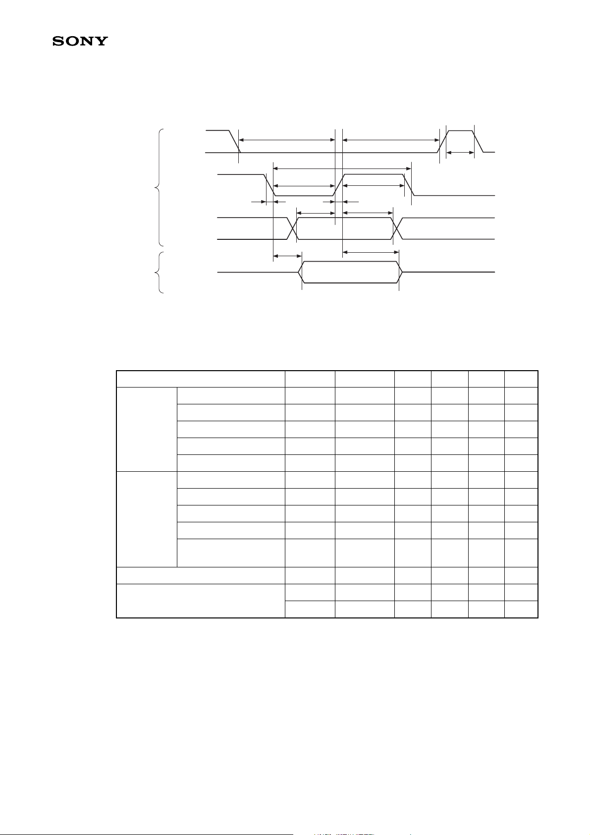
Horizontal Timing of RGB Interface (RGB I/F / FlatLink3G)
ACX567AKM-7
DE
HS
Data
PCLK
HFP
HBL
HDISP
HSW
HBP
HP
Horizontal Timing Diagram of RGB Interface
Horizontal Timing of RGB Interface (320 480 Mode)
(Ta = –30 to +70C, VDDI = 1.65 to 1.95V, VDD = 2.3 to 2.9V, VSS = 0V)
320 480 Mode
Item Symbol Condition Min. Typ. Max. Unit
Horizontal cycle HP Normal Mode 344 352 376 dots
Horizontal Low pulse width HSW Normal Mode 2 4 52 dots
Horizontal front porch HFP Normal Mode 2 16 52 dots
Horizontal back porch HBP Normal Mode 2 12 52 dots
Horizontal blanking period HBL Normal Mode 24 32 56 dots
Horizontal active area HDISP Normal Mode — 320 — dots
Pixel clock frequency PCLK Normal Mode 8.36 10.31 11.98 MHz
Note)
1. Signal rise and fall times are equal or less than 20ns.
2. Measuring of input signals are using 0.30 V
DDI for Low state and 0.70 VDDI for High state.
3. HP is multiples of eight PCLK.
4. Data lines can be set to “High” or “Low” during blanking time — Don’t care.
- 23 -
Page 24
General Timing Diagram of RGB Interface
ACX567AKM-7
VS
HS
PCLK
Data, DE
30%
HVPD
VSSU
30%
30%
70%
30%
HSSU
PCLKL
30%
DSU
70%
PCLKH
DHO
70%
70%
30%
70%
VSHO
30%
HSHO
30%
PCLKCYC
70%
General Timing Diagram of RGB Interface
General Timing of RGB Interface
Item Symbol Condition Min. Typ. Max. Unit
VS setup time VSSU 5 — — ns
VS hold time VSHO 5 — — ns
HS setup time HSSU 5 — — ns
HS hold time HSHO 5 — — ns
Phase difference of sync. signal
falling edge
HVPD — 0 — ns
Pixel clock Low time PCLKL 15 — — ns
Pixel clock High time PCLKH 15 — — ns
Data setup time DSU 5 — — ns
Data hold time DHO 5 — — ns
Note)
1. Signal rise and fall times are equal or less than 20ns.
2. Measuring of input signals are using 0.30 V
DDI for low state and 0.70 VDDI for High state.
- 24 -
Page 25
Serial Interface
Timing of Serial Interface
ACX567AKM-7
tcsh
tshw
tsdh
toh
Host
Driver
SPI_CS
SPI_CLK
SPI_DI
(Host)
SPI_DO
(Driver)
Hi-Z
tcss
tscyc
tslw
tf
tsds
tacc
tr
Timing Diagram of Serial Interface
Timing of Serial Interface
(Ta = –30 to +70C, VDDI = 1.65 to 1.95V, VDD = 2.3 to 2.9V, VSS = 0V)
Item Symbol Condition Min. Typ. Max. Unit
Serial clock cycle tscyc SPI_CLK 100 — — ns
SCL High pulse width tshw SPI_CLK 35 — — ns
Write mode
SCL Low pulse width tslw SPI_CLK 30 — — ns
tchw
Data setup time (write) tsds SPI_DI 20 — — ns
Data hold time tsdh SPI_DI 20 — — ns
Serial clock cycle tscyc SPI_CLK 150 — — ns
SCL High pulse width tshw SPI_CLK 60 — — ns
Read mode
SCL Low pulse width tslw SPI_CLK 60 — — ns
Access time (Note 1) tacc SPI_DO 10 — 50 ns
Output disable time
(Note 1)
toh SPI_DO 15 — 50 ns
XSC High pulse width tchw SPI_CS 40 — — ns
tcss SPI_CS 30 — — ns
XSC - SCL time
tcsh SPI_CS 35 — — ns
Note)
1. The output signal’s rise and fall times are to be stipulated maximum 15ns.
2. The input signal’s rise and fall times are equal or less than 15ns.
3. Logic High and Low levels of input signals are specified as 0.3 V
DDI for High state.
V
DDI for Low state and 0.7
4. SPI_CLK can be High or Low during off state.
- 25 -
Page 26
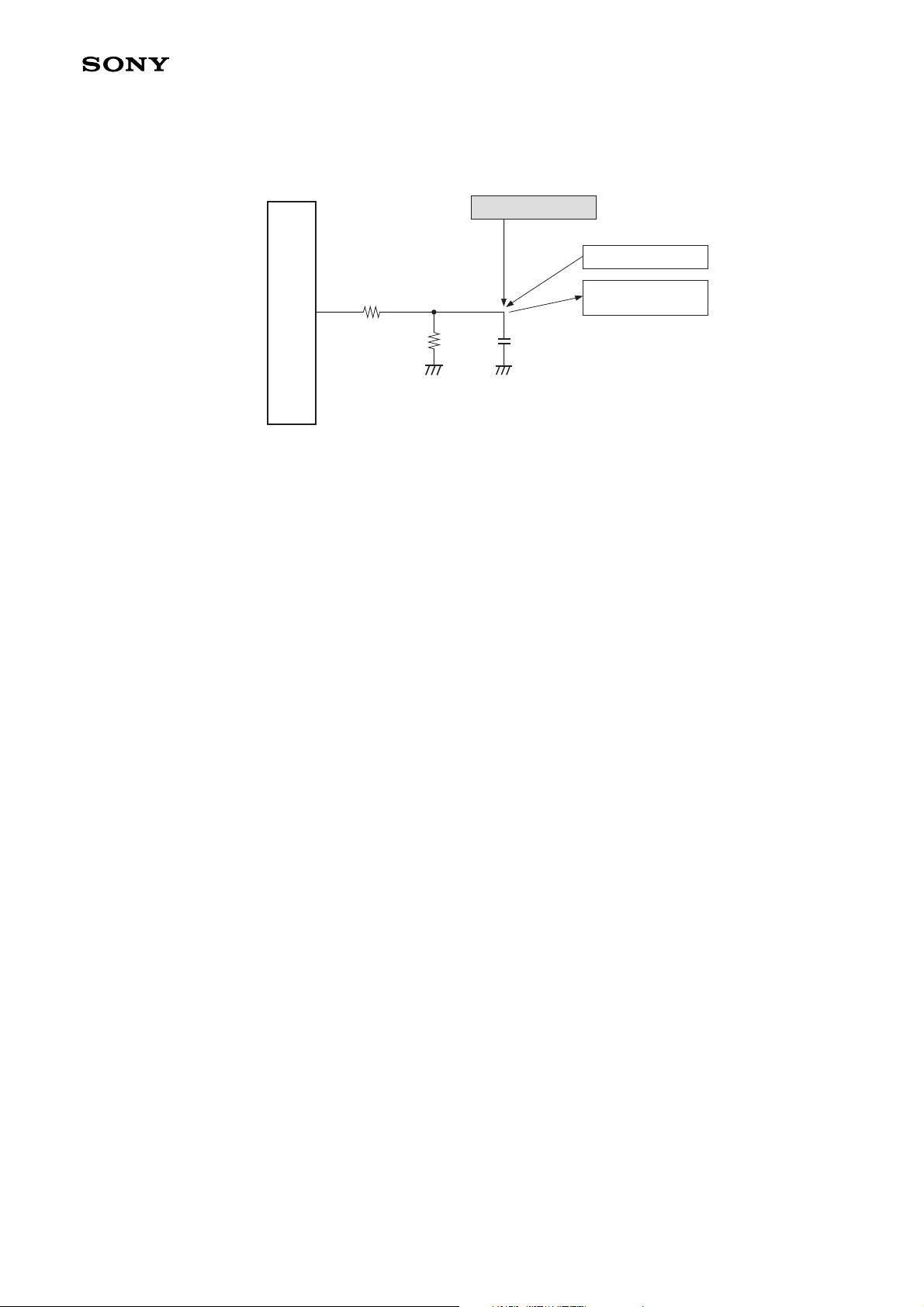
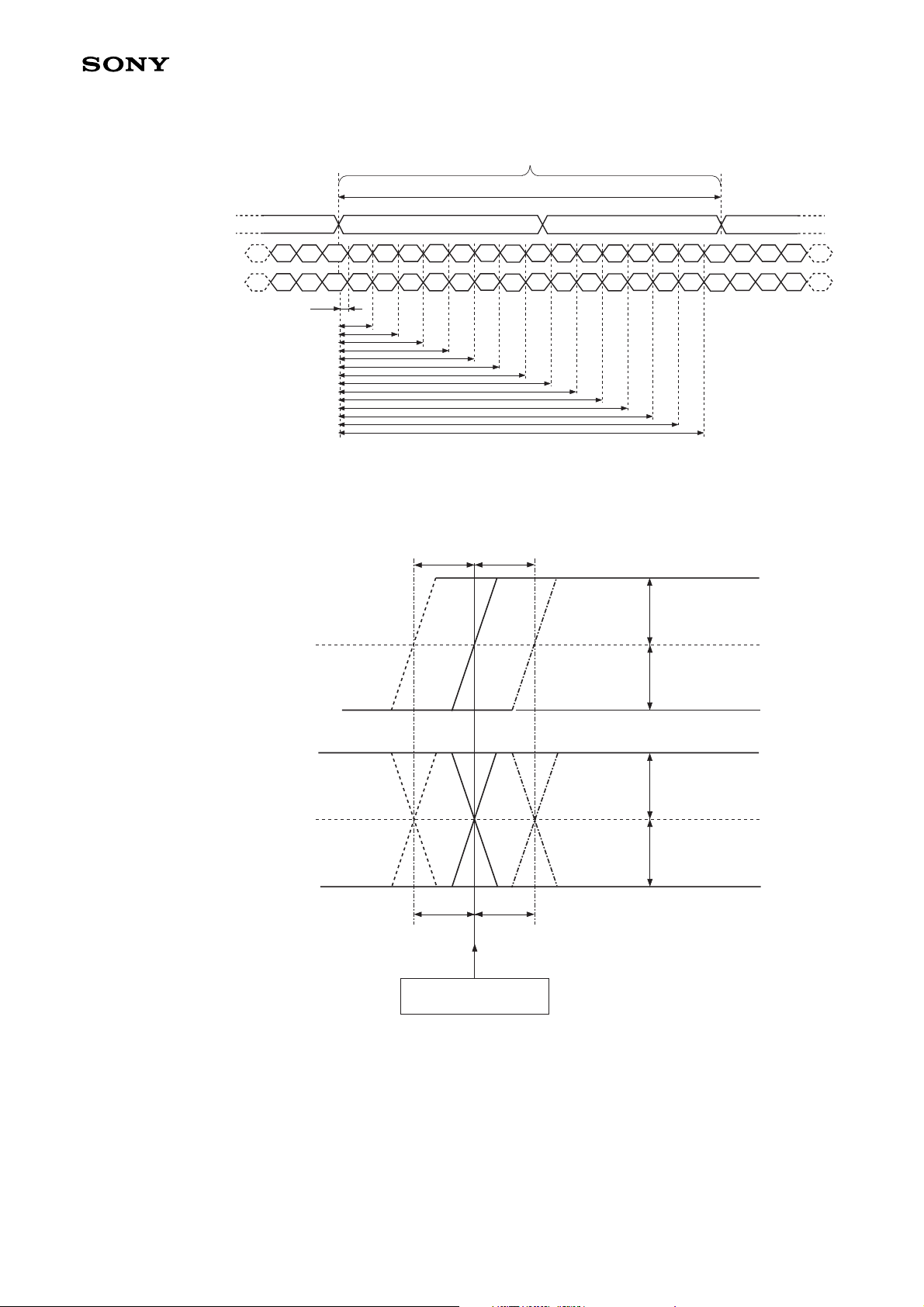
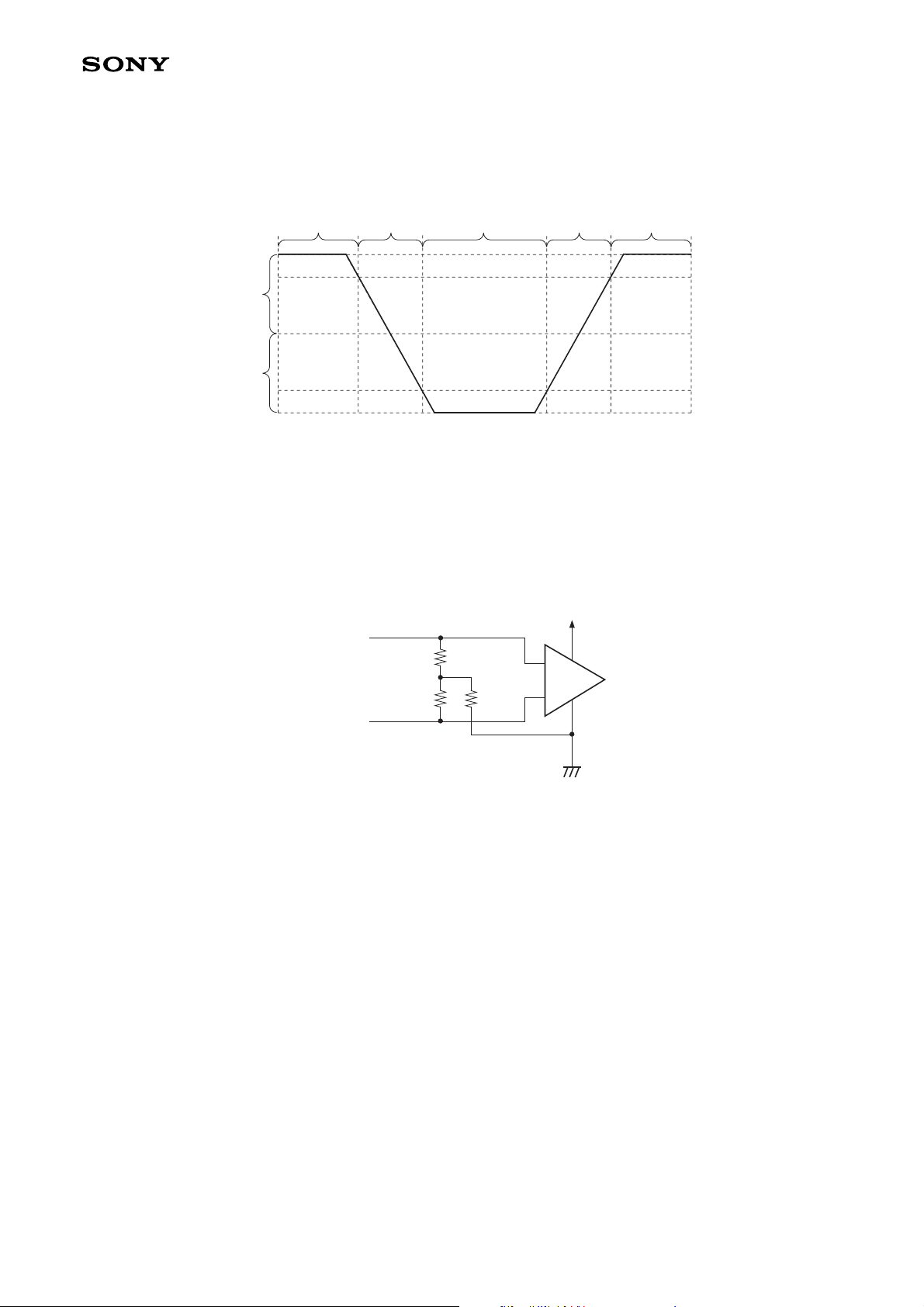
tACC and tOH Measurement Condition for Serial Interface
Measurement Condition and Setup
Measurement point
IC
Measurement Condition and Setup
Note)
Capacitances and resistances of the oscilloscope’s probe must be included in external
components in these measurements.
ACX567AKM-7
Data generator
Oscilloscope
(Note)
- 26 -
Page 27

Minimum Measurement
ACX567AKM-7
SCL
SDA
(Pulled-up)
SDA
(Pulled-down)
SPI_DO
30%
100%
t
ACC
0%
Minimum Measurement Timing
20Ω (±5%)
3kΩ (±5%)
8pF (±10%)
70%
t
CH
Measurement point
0%
100%
SPI_DO
Measurement Circuit (Pull-down Resistor)
Measurement point
8pF (±10%)
20Ω (±5%)
VDDI
3kΩ (±5%)
Measurement Circuit (Pull-up Resistor)
- 27 -
Page 28

Maximum Measurement
ACX567AKM-7
SCL
SDA
(Pulled-up)
SDA
(Pulled-down)
SPI_DO
70%
30%
t
ACC
20%
80%
Maximum Measurement Timing
20Ω (±5%)
3kΩ (±5%)
30pF (±10%)
tCH
0%
100%
Measurement point
SPI_DO
Measurement Circuit (Pull-down Resistor)
Measurement point
30pF (±10%)
20Ω (±5%)
VDDI
3kΩ (±5%)
Measurement Circuit (Pull-up Resistor)
- 28 -
Page 29

ACX567AKM-7
One Pixel Data Memory
The display module includes one pixel (24 bit: 8 bits for R, G and B). This memory includes information of
the first active pixel on the frame (pixel: 0, 0 = first active line and pixel on the display) from RGB I/F.
The purpose of this memory is that there is possible the check that D[23:0]-lines are working correctly.
The information of this memory is read via serial interface.
There will not be any abnormal visible effect on the display when there is written RGB information to this
memory or read RGB information via the serial interface from this memory at the same time.
Note)
Data read from the one pixel memory not guaranteed if read during the period when first pixel is
being written to the display from the FlatLink3G /RGB interface as indicated below: -
VS
Data
DE
HS
DE
HS
Data
VFP
VSW
VBL
VBP
VP
Zoom Image
1 pixel data
VDISP
1 line data
PCLK
Data invalid
Note)
There will be no abnormal visible effects on the display when RGB data is written to the one pixel
memory or when data is read from the one pixel memory via the read registers.
- 29 -
Page 30

ACX567AKM-7
Serial Interface (SPI)
General Description
The Module uses a 3-wire 9-bit serial interface. The chip-select SPI_CS (active Low) enables and disables
the serial interface. RESETX (active Low) is an external reset signal.
SPI_CLK is the serial data clock and SPI_DI/DO is serial data.
Serial data must be input to SPI_DI/DO in the sequence D/CX, D7 to D0. The Graphics Controller Chip
reads the data at the rising edge of SPI_CLK signal. The first bit of serial data D/CX is data/command flag.
When D/CX = “1”, D7 to D0 bits are display RAM data or command parameters. When D/CX = “0” D7 to
D0 bits are commands.
Command Write
The host CPU drives the SPI_CS pin Low and starts by setting the D/CX-bit on SPI_DI/DO. The bit is read
by the display on the first rising edge of SPI_CLK. On the next falling edge of SPI_CLK the MSB data bit
(D7) is set on SPI_DI by the CPU. On the next falling edge of SPI_CLK the next bit (D6) is set on SPI_DI.
This continues until all 8 Data bits have been transmitted as shown below.
Command
Command or parameter
XCS
Host
SDA
0
D7
D6
D5
D4 D3
D2
D1
D0
D/C
D7
D6
D5
D4
D3
D2
D1
D0
SCL
There is a possibility of Low level input at first SPI_CLK.
Command Write
Read Functions
The host read mode means that the host reads information from the display module (display driver) via the
serial interface. The display driver sends data to the host on a falling edge of SCL and the host reads data
on a rising edge of SCL. After reading operation there is a XCS High pulse before next command is sent.
Reading Commands 05h, 06h, 07h, 08h, DAh, DBh, DCh
Host
Driver
CSX
SCL
MPU SDA
LCD SDA
Read command
0 D7 D6 D5 D4 D3 D2 D1 D0
Hi-Z
D7 D6 D5 D4 D3 D2 D1 D0
ID data Next command
Hi-Z
0 D7 D6 D5 D4 D3 D2 D1 D0
MCU data Tx start
LCD data Tx start MCU data Tx start
8-bit Reading Function without Dummy Clock Cycle
- 30 -
Page 31

ACX567AKM-7
Display Module Data Transfer Recovery
If there is a break in data transmission while transferring command, Frame Memory Data or Multiple
Parameter command Data, before a whole byte has been completed, then the Display Module will have
reset the interface such that it will be ready to receive the same byte re-transmitted when the chip select
line (SPI_CS) is next activated.
See the following example:
Host
SPI_CS
SPI_DI/DO
SPI_CLK
Command/
Parameter
D7 D6 D5 D4
D/C
Break
Command or Parameter
D7 D6 D5 D4 D3 D2 D1 D0
D/C
Serial Interface Break
If a 1 or more parameter command is being sent and a break occurs while sending any parameter before
the last one and if the host then sends a new command rather than retransmitting the parameter that was
interrupted, then the parameters that were successfully sent are stored and the parameter where the break
occurred is rejected. The interface is ready to receive next byte as shown below:
1. Middle of frame
Brake
Command
Parameter 1
Stored to register
Parameter 2
The old value is
kept on the register
Command
2. Bitween frames
Without break
Command 1
With break
Command 1
Parameter 1
Parameter 1
Stored to register
Parameter 2
Parameter 2
The old value is
kept on the register
Break
Command 2
Serial Interface Break During Parameter
Parameter 3
Parameter 2
The old value is
kept on the register
Parameter
Command 2
for
- 31 -
Page 32

ACX567AKM-7
Display Module Data Transfer Pause
It will be possible when transferring Frame Memory Data, Command or Multiple Parameter Data to invoke
a pause in the data transmission. If the Chip Select Line is released after a whole byte of Frame Memory
Data, Command or Multiple Parameter Data has been completed, then the Display Module will wait and
continue the Frame Memory Data, Command or Parameter Data Transmission from the point where it was
paused as shown below:
Pause
Host
SPI_CS
SPI_DI/DO
SPI_CLK
Command/Parameter
D3 D2 D1 D0
D4
Serial Interface Pause
There are 4 cases when this kind of pause is possible:
(1) Command - Pause - Command
(2) Command - Pause - Parameter
(3) Parameter - Pause - Command
(4) Parameter - Pause - Parameter
Command or Parameter
D7 D6 D5 D4 D3 D2 D1 D0
D/C
- 32 -
Page 33

ACX567AKM-7
Display Module Data Transfer Modes
The Module has one color mode for transferring data to the display RAM. This is 3-bit color per pixel.
The data format is described for the interface. Data can be downloaded to the Frame Memory by 2 methods.
Method 1
The Image data is sent to the Frame Memory in successive Frame writes, each time the Frame Memory
is filled, the Frame Memory pointer is reset to the start point and the next Frame is written.
Start
Stored partial
frame memory
write
Image data
frame 1
Image data
frame 2
Image data
frame 3
Stop
Any
command
Method 2
Image Data is sent and at the end of each Frame Memory download, a command is sent to stop Frame
Memory Write. Then Start Memory Write command is sent, and a new Frame is downloaded.
Start
Stored partial
frame memory
write
Note)
Image data
frame 1
These apply to Data Transfer Color mode on the Serial interface.
Any
command
Stored partial
frame memory
write
Image data
frame 2
Any
command
Stop
Any
command
- 33 -
Page 34

Power Functions
Power ON and OFF Sequences
VDD_18 and VBATT can be applied in any order.
BATT and VDD_18 can be powered down in any order.
V
During power off, if LCD is in the Sleep Out mode, V
after RESETX has been released.
During power off, if LCD is in the Sleep In mode, V
RESETX has been released.
SPI_CS can be applied at any timing or can be permanently grounded. RESETX has priority over SPI_CS.
Note)
1. There will be no damage to the display module if the power sequences are not met.
2. There will be no abnormal visible effects on the display panel during the Power On/Off Sequences.
3. There will be no abnormal visible effects on the display between end of Power On Sequence and
4. If RESETX line is not held stable by host during Power On Sequence as defined in Sections P.35
ACX567AKM-7
BATT and VDD_18 must be powered down minimum 120ms
DD_18 or VBATT can be powered down minimum 0ms after
before receiving Sleep Out command. Also between receiving Sleep In command and Power Off
Sequence.
and P.36, then it will be necessary to apply a Hardware Reset (RESETX) after Host Power On
Sequence is complete to ensure correct operation.
Otherwise function is not guaranteed.
- 34 -
Page 35

ACX567AKM-7
Case-1. RESETX line is held High or unstable by host at power on
If RESETX line is held High or unstable by the host during power on, hardware reset will be applied after both
BATT and VDD_18 have been applied - otherwise correct functionality is not guaranteed. There is no timing
V
restriction upon this hardware reset.
PW = +/– no limit
tr
tfPW = +/– no limit
VDD_18
V
BATT
Time when the latter power voltage signal rises up to 90% of
its typical value. e.g. when V
defined at a cross point of 90% of 2.5/2.75V, not 90% of 2.3V.
Time when the former power voltage signal falls down to 90%
of its typical value. e.g. when V
defined at a cross point of 90% of 2.5/2.75V, not 90% of 2.3V.
BATT
comes later. This time is
BATT
falls earlier. This time is
PWXCS = +/– no limit
tf
trPWXCS = +/– no limit
SPI_CS
tr
PWXRES = + no limit
RESETX
(Power down in
Sleep Out mode)
tr
PWXRES = + no limit
30%
PWXRES1 = Min. 120ms
tf
RESETX
(Power down in
Sleep In mode)
30%
tf
PWXRES2 = Min. 0ns
tfPWXRES1 is applied to RESETX falling in Sleep Out mode.
tf
PWXRES2 is applied to RESETX falling in Sleep In mode.
Note: Unless otherwise specified, timings herein show cross point at 50% of signal/power level.
Power ON/OFF Sequence in Case 1
- 35 -
Page 36

ACX567AKM-7
Case-2. RESETX line is held Low by host at power on
If RESETX line is held Low (and stable) by the host during power on, then the RESETX must be held Low for
minimum 10s after both V
BATT and VDD_18 have been applied.
PW = +/– no limit
tr
VDD_18
tf
PW = +/– no limit
V
BATT
Time when the latter power voltage signal rises up to 90% of
its typical value. e.g. when VBATT comes later. This time is
defined at a cross point of 90% of 2.5/2.75V, not 90% of 2.3V.
Time when the former power voltage signal falls down to 90%
of its typical value. e.g. when VBATT falls earlier. This time is
defined at a cross point of 90% of 2.5/2.75V, not 90% of 2.3V.
PWXCS = +/– no limit
tf
trPWXCS = +/– no limit
SPI_CS
tr
PWXRES = Min. 10µs
RESETX
(Power down in
Sleep Out mode)
tr
PWXRES = Min. 10µs
tf
PWXRES1 = Min. 120ms
RESETX
(Power down in
Sleep In mode)
tf
PWXRES2 = Min. 0ns
tfPWXRES1 is applied to RESETX falling in Sleep Out mode.
PWXRES2 is applied to RESETX falling in Sleep In mode.
tf
Note: Unless otherwise specified, timings herein show cross point at 50% of signal/power level.
Power ON/OFF Sequence in Case 2
- 36 -
Page 37

Sleep Out Sequence 1 (I/F: FlatLink3G, Sleep Mode Normal Mode)
VBATT
VDD_18
RESETX
ACX567AKM-7
SPI_CS
SPI_CLK/
SPI_DI
CLK/D+/–
Display Image
Unsettled
Sleep Out (11h) and Display On (29h) Command
Active
Active
6 Frames
Black (Display Off) Image
Sleep In Sequence 1 (I/F: FlatLink3G, Normal Mode Sleep Mode)
VBATT
VDD_18
RESETX
SPI_CS
SPI_CLK/
SPI_DI
CLK/D+/–
Display Image
Active
Active
Sleep In (10h) Command
2 Frames (Min.)
Black (Display Off) Image
Active
Unsettled
- 37 -
Page 38

Reset Timing
ACX567AKM-7
RESX
Display Status
Tnr
Normal operation
Tst
Trw
Resetting
Tr t
Initial condition
(Default for HW reset)
Reset Timing
Reset Timings
Symbol Item Min. Typ. Max. Unit
Tnr Negative noise pulse — — < 5 s
Trw Reset pulse width 10 — — s
——< 5 (Note 1)ms
Trt Reset cancel time
——120 (Note 2, 3)ms
Tst Reset start time 5 — 10 s
Note)
1. When reset applied during Sleep in mode.
2. When reset applied during Sleep out mode.
3. It is necessary to wait 5ms after releasing XRES before sending commands.
Also Sleep out command cannot be sent for 120ms.
4. The reset cancel time includes also required time for loading ID bytes (or similar) from NVM to ID (or
similar) registers.
This loading is done every time within 5ms when HW reset is applied.
5. During the resetting period (at the end of Tst period), the display will be blanked immediately and
then return to default condition for hardware reset.
6. Spike rejection also applies during a valid reset pulse as shown below:
10 to 20µs
"RESET" is accepted.
10 to 20µs
20ns
Lass than 20ns width positive spike will be rejected.
Positive Noise Spike During Reset
- 38 -
Page 39

In-Panel Photo Sensing Device Controller
Block Diagram (Signal Flow Chart)
ACX567AKM-7
Output Interface
Manual B/L Control
(command I/F)
(video I/F)
Control
Registers
Picture Analyzer
IC supplier’s Intellectual Property
Backlight brightness
Picture Enhancer
Dimming controller
PWM_LBL
integrator
Backlight switch
Backlight PWM driver
reduction coefficient
Gamma Correction
- 39 -
Page 40

ACX567AKM-7
Interface
Software Interface
The In-panel Light Sensor has some optional function provided by register setting. Some of the resister is
public and open to LCD module interface.
Register name Size of registers Function Default Access
LBV[7:0] 8bit Write LCD brightness 00h
0x51 (Write)
0x52 (Read)
BCTRL 1bit Control display 0b
LD 1bit Control display 0b
BL 1bit Control display 0b
LB 1bit Control display 0b
CM[1:0] 2bits Content auto backlight control 00b
CMB[7:0] 8bit CABC minimum brightness 00h
Register Connection Overview
Public/Private Control registers are connected to each blocks as shown below.
Host Commands
PWM_LBL
Image Data
WRLCDBV
WRCTRLL Bit D5
WRCTRLL Bit D1 (DB) auto/manual
WRCTRLL Bit D3 (DD) LCD dimming
WRCTRLL Bit D2 (BL) final on/off
C[1:0]
WRCABC[7:0]
PWM
SW
NVM
Manual
B/L
Control
Dimming
CABC
Integrator
Dimming
Bright info
CABC
Block
CABC &
Gamma
Integrator
Gamma info
Image Data
0x53 (Write)
0x54 (Read)
0x55 (Write)
0x56 (Read)
0x5E (Write)
0x5F (Read)
Gamma
8bit resolution
D/A converter
PanelDriver ICFPC
Source Data
- 40 -
Page 41

Backlight Brightness Selector
User can select to use either manual B/L values (WRLCDBV[7:0]) or 8’b0.
Manual B/L values (WRLCDBV[7:0]) can set between 0 (minimum) and 255 (maximum).
In case of using external ALS, user should be set DB = “0”.
DB
ACX567AKM-7
8’b0
WRLCDBV[7:0]
To dimming controller
Dimming Controller
A dimming function is used when changing form one brightness level to another.
Dimming function is control 0x53 register for display and 0x63 register for keyboard respectively.
Dimming Off
Luminance
Hysteresis step up
Time
Dimming On
Luminance
Dimming on (divided by 28 frames)
Time
- 41 -
Page 42

ACX567AKM-7
Contents Auto Backlight Function
Contents Adaptive Function is provided by IC vender’s IP.
Use can control only CM[1:0] setting defined by 0x55 register.
CM[1:0] is defined by below table.
CM1 CM0 Function Reduction ratio
00CABC off 0
01Desk top mode < 10%
10Still image mode > 30%
11Moving image mode > 30%
Definition of mode:
CM[1:0] = 00 (Off mode): Content Auto Backlight control is totally off.
CM[1:0] = 01 (Desk top mode): Optimized for UI image. It is kept image quality as much as possible.
Target power consumption reduction ratio 10% or less.
CM[1:0] = 10 (Still image mode): Optimized for still picture. Some image quality degradation would be
acceptable. Target power consumption reduction ratio more than 30%.
CM[1:0] = 11 (Moving image mode): Optimized for moving image. If is focused on the biggest power
reduction with image quality degradation. Target power consumption reduction ratio more than 30%.
LCD Backlight Control Integrator
Configuration
When CM[1:0] is 00, Contents adaptive function is turned off and minimum brightness limitation;
CMB[7:0] must not applied to the result.
When CM[1:0] is not 00, Contents adaptive function is turned on and calculated CABC and LABC must
not be smaller than CMB[7:0].
C[1:0] > 0 C[1:0] = 0
WRLCDBV < WRCABC WRLCDBV WRLCDBV
CABC WRLCDBV < WRCABC
WRLCDBV WRCABC WRCABC WRLCDBV
WRLCDBV < WRCABC — —
CABC WRLCDBV WRCABC
WRLCDBV WRCABC WRLCDBV CABC WRLCDBV
- 42 -
Page 43

Commands for Serial Interface
Command Set
ACX567AKM-7
Operational code
[HEX]
Function
Number of
parameter bytes
Parameters
0No operation 0 —
1Software reset 0 —
5
Read number of parity
errors
1—
6Read red color 1Red information from one pixel memory
7Read green color 1Green information from one pixel memory
8Read blue color 1Blue information from one pixel memory
10 Sleep in 0 —
11 Sleep out 0 —
28 Display off 0 —
29 Display on 0 —
36 Memory access control 1 1 byte for memory access definition
3A Interface color format 1 1 byte for color format
51 Write LCD brightness 1
52 Read LCD brightness 1
53 Write CTRL LCD 1
54 Read CTRL LCD 1
55
56
5E
5F
Write content auto
backlight control
Read content auto
backlight control
Write CABC minimum
brightness
Read CABC minimum
brightness
1
1
1
1
DA Read ID1 1 Fixed value (10h)
DB Read ID2 1 Module version
DC Read ID3 1 Module ID (XXh)
Note)
1. Undefined commands are working as a NOP (00h) command.
2. B0h to D9h and DEh to FFh are for factory use (Display manufacturer area).
After shipping these commands are acting as same as NOP (00h) commands for end customer.
3. Commands 10h, 28h, 29h, and 36h (Bits: B4, only) are updated during V-sync when the display
module is in Sleep Out mode to avoid abnormal visual effects.
During Sleep In mode, these commands are updated immediately.
- 43 -
Page 44

Command Description
NOP (00h)
ACX567AKM-7
00H
NOP (No operation)
D/CX D7 D6 D5 D4 D3 D2 D1 D0 HEX
Command 0 0 0 0 0 0 0 0 0 00
Parameter No parameter
Description This command is an empty command. It does not have any effect on the display module.
Restrictions
Register
availability
Default
Status
Normal mode, Sleep out
Partial mode, Sleep out
Sleep in
Status
Power on sequence
SW reset
HW reset
Availability
Yes
Yes
Yes
Default value
N/A
N/A
N/A
Flow chart
- 44 -
Page 45

ACX567AKM-7
Software Reset (01h)
01H SWRESET (Software reset)
D/CX D7 D6 D5 D4 D3 D2 D1 D0 HEX
Command 0 0 0 0 0 0 0 0 1 01
Parameter No parameter
When software reset command is applied, it causes software reset. It resets the
commands and parameters to their SW reset default values. (See default tables in each
Description
command description.) The display is blank (white in case of normally white display,
black in case of normally black display) immediately.
Note)
The single pixel memory content is unaffected by this command.
It is necessary to wait 5ms before sending new command following software reset.
If SW reset is applied during Sleep out mode, it is necessary to wait 120ms before
Restrictions
sending Sleep out command. Factory default settings are loaded from NVM during the
first 5ms after S/W reset command is sent.
SW reset command cannot be sent during Sleep out sequence.
Register
availability
Default
Flow chart
Status
Normal mode, Sleep out
Partial mode, Sleep out
Sleep in
Status
Power on sequence
SW reset
HW reset
SWRESET
Display whole
white screen
Set registers
to the SW
reset default
values
Sleep-in mode
Availability
Yes
Yes
Yes
Default value
N/A
N/A
N/A
Legend
Command
Parameter
Display
Action
Mode
Sequential
transfer
- 45 -
Page 46

ACX567AKM-7
Read Number of Parity Errors (05h)
05H RDNUMPE (Read Number of Parity Errors)
D/CX D7 D6 D5 D4 D3 D2 D1 D0 HEX
Command 0 0 0 0 0 0 1 0 1 05
1st parameter — P7 P6 P5 P4 P3 P2 P1 P0 xx
The first parameter returns the number of detected errors on the FlatLink3G interface: -
Description
Bits P[6:0] indicate the number of parity errors.
Bit P7 indicate there is an overflow in bits P[6:0].
Restrictions
Register
availability
Default
Flow chart
Status
Normal mode, Sleep out
Partial mode, Sleep out
Sleep in
Status
Power on sequence
SW reset
HW reset
RDBLUE
Send 1st
parameter
Reset P[7:0] to 00
Reset RDDST (09H) Bit D0 to "0"
Reset RDDSM (0E
H
H
) Bit D0 to "0"
Host
Display
Availability
Yes
Yes
Yes
Default value
00h
00h
00h
Legend
Command
Parameter
Display
Action
Mode
Sequential
transfer
- 46 -
Page 47

ACX567AKM-7
Read Red Color (06h)
06H RDRED (Read red color)
D/CX D7 D6 D5 D4 D3 D2 D1 D0 HEX
Command 0 0 0 0 0 0 1 1 0 06
1st parameter — R7 R6 R5 R4 R3 R2 R1 R0 xx
The first parameter is telling red color value of the first pixel of the frame when there is
used RGB I/F.
Description
16 bit format: R5 is MSB and R1 is LSB. R7, R6 and R0 are set to “0”.
18 bit format: R5 is MSB and R0 is LSB. R7 and R6 are set to “0”.
24 bit format: R7 is MSB and R0 is LSB.
See: P.29
Restrictions
Register
availability
Default
Flow chart
Status
Normal mode, Sleep out
Partial mode, Sleep out
Sleep in
Status
Power on sequence
SW reset
HW reset
RDRED
Send 1st
parameter
Display
Host
Availability
Yes
Yes
Yes
Default value
00h
00h
00h
Legend
Command
Parameter
Display
Action
Mode
Sequential
transfer
- 47 -
Page 48

ACX567AKM-7
Read Green Color (07h)
07H RDGREEN (Read green color)
D/CX D7 D6 D5 D4 D3 D2 D1 D0 HEX
Command 0 0 0 0 0 0 1 1 1 07
1st parameter — G7 G6 G5 G4 G3 G2 G1 G0 xx
The first parameter is telling green color value of the first pixel of the frame when there
is used RGB I/F.
Description
16 and 18 bit formats: G5 is MSB and G0 is LSB. G7 and G6 are set to “0”.
24 bit format: G7 is MSB and G0 is LSB.
See: P.29
Restrictions
Register
availability
Default
Flow chart
Status
Normal mode, Sleep out
Partial mode, Sleep out
Sleep in
Status
Power on sequence
SW reset
HW reset
RDGREEN
Send 1st
parameter
Display
Host
Availability
Yes
Yes
Yes
Default value
00h
00h
00h
Legend
Command
Parameter
Display
Action
Mode
Sequential
transfer
- 48 -
Page 49

ACX567AKM-7
Read Blue Color (08h)
08H RDBLUE (Read blue color)
D/CX D7 D6 D5 D4 D3 D2 D1 D0 HEX
Command 0 0 0 0 0 1 0 0 0 08
1st parameter — B7 B6 B5 B4 B3 B2 B1 B0 xx
The first parameter is telling blue color value of the first pixel of the frame when there is
used RGB I/F.
Description
16 bit format: B5 is MSB and B1 is LSB. B7, B6 and B0 are set to “0”.
18 bit format: B5 is MSB and B0 is LSB. B7 and B6 are set to “0”.
24 bit format: B7 is MSB and B0 is LSB.
See: P.29
Restrictions
Register
availability
Default
Flow chart
Status
Normal mode, Sleep out
Partial mode, Sleep out
Sleep in
Status
Power on sequence
SW reset
HW reset
RDGREEN
Send 1st
parameter
Host
Display
Availability
Yes
Yes
Yes
Default value
00h
00h
00h
Legend
Command
Parameter
Display
Action
Mode
Sequential
transfer
- 49 -
Page 50

ACX567AKM-7
Sleep In (10h)
10H SLPIN (Sleep in)
D/CX D7 D6 D5 D4 D3 D2 D1 D0 HEX
Command 0 0 0 0 1 0 0 0 0 10
Parameter No parameter
This command causes the LCD module to enter the minimum power consumption
mode. In this mode the DC/DC converter is stopped and panel scanning is stopped.
SPI and RGB I/F as well as Single Pixel Memory and Frame Memory are still working
and the memory keeps its contents. The FlatLink3G receiver is Low power mode.
Description
MCU will send PCLK, HS and VS information on FlatLink3G (if FlatLink3G mode is
used) or RGB I/F (if RGB I/F Mode is used) for Blank display after Sleep In command
and this information is valid during 2 frames after Sleep In command if there is used
Normal Display Mode On in Sleep Out -mode. The FlatLink3G receiver is powered
down after these 2 frames if FlatLink3G mode is used.
There is used an internal oscillator for blank display in Partial Mode On.
This command has no effect when module is already in Sleep in mode. Sleep in mode
can only be exit by the Sleep out command (11h). It is necessary to wait 5ms before
Restrictions
sending next command, this is to allow time for supply voltages and clock circuit to
stabilize. It is necessary to wait 120ms after sending Sleep out command (when in
Sleep in mode) before Sleep in command can be sent.
Register
availability
Default
Flow chart
SLPIN
Display whole
white screen
(No effect to
DISPON/DISPOFF
commands
Status
Normal mode, Sleep out
Partial mode, Sleep out
Sleep in
Status
Power on sequence
SW reset
HW reset
Drain charge
from LCD panel
Stop DC-DC converter
Stop internal oscillator
Sleep in mode
Availability
Yes
Yes
Yes
Default value
Sleep in mode
Sleep in mode
Sleep in mode
Legend
Command
Parameter
Display
Action
Mode
Sequential
transfer
- 50 -
Page 51

ACX567AKM-7
Sleep Out (11h)
11H SLPOUT (Sleep out)
D/CX D7 D6 D5 D4 D3 D2 D1 D0 HEX
Command 0 0 0 0 1 0 0 0 1 11
Parameter No parameter
This command turns off Sleep mode. In this mode the DC/DC converter is enabled and
panel scanning is started. MCU will start to send PCLK, HS and VS information on
FlatLink3G (if FlatLink3G mode is used) or RGB I/F (if RGB I/F mode is used) before
Sleep Out command and this information is valid at least 2 frames before Sleep Out
Description
command, if there is left Sleep In -mode to Sleep Out -mode in Normal Display Mode
On. The FlatLink3G receiver is High power mode and stabilized within 2 image frames
(2 VS) after this command, if there is left Sleep In -mode to Sleep Out -mode in Normal
Display Mode On and FlatLink3G mode is used.
There is used an internal oscillator for blank display in Partial Mode On.
This command has no effect when module is already in Sleep out mode. Sleep out
mode can only be exit by the Sleep in command (10h). It is necessary to wait 5ms
Restrictions
before sending next command, this is to allow time for supply voltages and clock circuit
to stabilize. It is necessary to wait 120ms after sending Sleep In command (when in
Sleep out mode) before Sleep out command can be sent.
Register
availability
Default
Flow chart
SLPOUT
Start internal oscillator
Start up
DC-DC converter
Charge offset voltage
for LCD panel
Status
Normal mode, Sleep out
Partial mode, Sleep out
Sleep in
Status
Power on sequence
SW reset
HW reset
Display whole
white screen
(No effect to
DISPON/DISPOFF
commands
Display image
according to the
current command
setting
Sleep out mode
Availability
Yes
Yes
Yes
Default value
Sleep in mode
Sleep in mode
Sleep in mode
Legend
Command
Parameter
Display
Action
Mode
Sequential
transfer
- 51 -
Page 52

ACX567AKM-7
Display Off (28h)
28H DISPOFF (Display off)
D/CX D7 D6 D5 D4 D3 D2 D1 D0 HEX
Command 0 0 0 1 0 1 0 0 0 28
Parameter No parameter
This command is used for entering into Display off mode. In this mode the output from
RGB I/F is disabled and white page inserted. Also the output of partial frame memory
is disabled. This command does not change contents of RGB I/F nor partial frame
memory. This command does not change any other status. There will be no abnormal
visible effect on the display when Display off command is sent. Exit from this command
by Display on (29h).
Description
Example:
RGB interface/
Partial framememory
Display
Restrictions This command has no effect when module is already in display off mode.
Register
availability
Default
Status
Normal mode, Sleep out
Partial mode, Sleep out
Sleep in
Status
Power on sequence
SW reset
HW reset
Availability
Yes
Yes
Yes
Default value
Display off
Display off
Display off
Legend
Command
Flow chart
Display on
DISPOFF
Display off
- 52 -
Parameter
Display
Action
Mode
Sequential
transfer
Page 53

ACX567AKM-7
Memory Access Control (36h)
36H MADCTL (Memory access control)
D/CX D7 D6 D5 D4 D3 D2 D1 D0 HEX
Command 0 0 0 1 1 0 1 1 0 36
Parameter 1 B7 B6 B5 B4 B3 00 00 00 xx
This command defines the updating order of panel in the normal mode, updating order
of partial frame memory and scanning order in partial mode. This command makes no
change on the other driver status.
Description
Bit
B7
Page address order
B6
Column address order
B5
Page (colmun selection)
B4
Vertical order
B3
RGB/BGR order
Name
Default value
B7, B6 and B5 control writing direction to partial frame memory.
B7 and B6 control the updating order of the panel in normal
mode.
B4 controls vertical refresh direction in partial mode.
Color selector switch control.
(0 = RGB color filter panel, 1 = BGR color filter panel)
All five bits (B7 - B3) affects to partial mode. The description of B3 is below.
Only bits B7, B6 and B3 affect to normal mode. Behavior of B7 and B6 in normal mode
is explained in P.20 and 21. The description of B3 is below.
B3 – RGB - BGR Order
B3 = "0" B3 = "1"
Driver IC
RGB RGB
RGB
LCD Panel
RGB RGB
RGB
LCD Panel
Driver IC
Restrictions D2, D1 and D0 are set to “000” internally.
Status
Normal mode, Sleep out
Partial mode, Sleep out
Sleep in
MADCTL command affects the display module according to the current mode of
operation. The table below summaries the action of MADCTL for each mode: Register
availability
Bit
B7
Panel Scan Direction
B6
B5
Updates Road Register 09h Bits D28, D27
and 0Bh Bits D5, D4 only
B4
B3
Update Read Register 09h Bit D26 and 0Bh Bit D3 only
Normal Mode On
In both modes, the status register 09h and 0Bh are always updated immediately.
- 53 -
Availability
Yes
Yes
Yes
Partial Mode On
Partial Frame Memory Pointer Control
Frame Memory Read and
Panel Scanning Direction Control
Page 54

36H MADCTL (Memory access control)
ACX567AKM-7
Default
Flow chart
Status
Power on sequence
SW reset
HW reset
Default value
B7 = 0, B6 = 0, B5 = 0, B4 = 0, B3 = 0, B2 = 0, B1 = 0, B0 = 0
No change
B7 = 0, B6 = 0, B5 = 0, B4 = 0, B3 = 0, B2 = 0, B1 = 0, B0 = 0
Legend
Command
Parameter
MADCTL
Parameter
B[7:0]
Display
Action
Mode
Sequential
transfer
- 54 -
Page 55

ACX567AKM-7
Interface Color Format (3Ah)
3AH COLMOD (Interface color format)
D/CX D7 D6 D5 D4 D3 D2 D1 D0 HEX
Command 0 0 0 1 1 1 0 1 0 3A
Parameter 1 xx D6 D5 D4 xx xx xx xx xx
This command defines the format of FlatLink3G /RGB I/F image data, which is
transferred via interface. The formats are shown in the table below.
Description
Restrictions
Register
availability
Default
Interface format
Not defined
Not defined
Not defined
Not defined 0
Not defined 1
16 bits/pixel 1
18 bits/pixel 1
24 bits/pixel 1
D6
D5
D4
0
0
0
0
0
1
0
1
0
1
1
0
0
0
1
1
0
1
1
Not defined in the table above are invalid and will not change the current interface color
format until valid value is received.
Status
Normal mode, Sleep out
Partial mode, Sleep out
Sleep in
Status
Power on sequence
SW reset
HW reset
Availability
Yes
Yes
Yes
Default value
24 bits/pixel
No change
24 bits/pixel
Flow chart
18 bits/pixel
COLMOD
Parameter
[x101xxxx]
16 bits/pixel
Legend
Command
Parameter
Display
Action
Mode
Sequential
transfer
- 55 -
Page 56

ACX567AKM-7
Write LCD Brightness (51h)
51H WRLCDBV (Write LCD Brightness)
D/CX D7 D6 D5 D4 D3 D2 D1 D0 HEX
Command 0 0 1 0 1 0 0 0 1 51
Parameter 1 LBV7 LBV6 LBV5 LBV4 LBV3 LBV2 LBV1 LBV0
00..FF
This command is used to adjust the brightness value of the display when in Manual
Brightness Mode. (When WRCTLL (53H) Bits D5 (BCTRL) = “1” and D1 (DB) = “0”
The relationship between this value and output brightness of the display in luminance
Description
terms is defined in the Display Module Specification.
Principally LBV[7:0] = 00H means minimum brightness, LBV[7:0] = FFH means
maximum brightness.
X = Don’t care
Restrictions
Register
availability
Default
Flow chart
Status
Normal Mode On, Idle Mode Off, Sleep Out
Normal Mode On, Idle Mode On, Sleep Out
Partial Mode On, Idle Mode Off, Sleep Out Yes
Partial Mode On, Idle Mode On, Sleep Out Yes
Sleep In
Status
Power on sequence
SW reset
HW reset
WRPFD
WRPFD
LBV[7:0]
LBV[7:0]
New display
New display
brightness value
brightness value
loaded
loaded
Default value
Command
Command
Parameter
Parameter
Sequential
Sequential
00h
00h
00h
Legend
Legend
Display
Display
Action
Action
Mode
Mode
transfer
transfer
Availability
Yes
Yes
Yes
- 56 -
Page 57

ACX567AKM-7
Read LCD Brightness Value (52h)
52H RDLCDBV (Read LCD Brightness Value)
D/CX D7 D6 D5 D4 D3 D2 D1 D0 HEX
Command 0 0 1 0 1 0 0 1 0 52
Parameter 1 LBV7 LBV6 LBV5 LBV4 LBV3 LBV2 LBV1 LBV0 xx
This command returns the brightness value of the LCD.
The relationship between this value and output brightness of the LCD in luminance
terms is defined in the LCD Module Specification.
Principally LBV[7:0] = 00H means minimum brightness, LBV[7:0] = FFH means
maximum brightness.
When WRCTRLL (53H) Bits D5 (BCTRL) = “1” and D1 (DB) = “0” (Manual Brightness
Mode), then RDLCDBV LBV[7:0] returns the value of WRLCDBV (51H) LBV[7:0].
When WRCTRLL (53H) Bits D5 (BCTRL) = “1”, D4 (A) = “1” and D1 (LB) = “1”
Description
(Automatic Brightness Mode), then RDLCDBV LBV[7:0] returns the current value of
LCD Brightness after the dimming function.
When WRCTRLL (53H) Bits D5 (BCTRL) = “1” and D4 (A) = “0” and DB = “1”, then
RDLCDBV LBV[7:0] returns then RDLCDBV LBV[7:0] returns the current value of LCD
Brightness after the dimming function.
When WRCTRLL (53H) Bit D5 (BCTRL) = “0” then RDLCDBV LBV[7:0] returns 00H.
When in Sleep In Mode, RDLCDBV LBV[7:0] returns 00H.
Restrictions
Register
availability
Default
Flow Chart
X = Don’t care
Status
Normal Mode On, Idle Mode Off, Sleep Out
Normal Mode On, Idle Mode On, Sleep Out
Partial Mode On, Idle Mode Off, Sleep Out Yes
Partial Mode On, Idle Mode On, Sleep Out Yes
Sleep In
Status
Power on sequence
SW reset
HW reset
Read RDLCDBV
Send 1st
parameter
Default value
Host
Display
Availability
Yes
Yes
Yes
00h
00h
00h
Legend
Command
Parameter
Display
Action
Mode
- 57 -
Sequential
transfer
Page 58

ACX567AKM-7
Write CTRL LCD (53h)
53H WRCTRLL (Write CTRL LCD)
D/CX D7 D6 D5 D4 D3 D2 D1 D0 HEX
Command 0 0 1 0 1 0 0 1 1 53
Parameter 1 X X
BCTRL
XLDBLX X
00..FF
This command is used to control ambient light and brightness.
Bit D5 - BCTRL (Brightness Control Block On/Off)
“0” = Off (Brightness registers RDLCDBV (52H) LBV[7:0] = 00H PWM outputs
PWM_LBL is Low).
“1” = On (Brightness registers RDLCDBV (52H)
Bit D3 - LD (LCD Dimming)
“0” = LCD Dimming is Off
Description
“1” = LCD Dimming is On
Bit D2 - BL (Backlight On/Off)
“0” = Off
(Completely turn off backlight circuit. Control Lines PWM_LBL must be Low).
“1” = On
If B it D5 (B CTRL) i s chang ed whi l e Bit D 3 (DD) = “1” (Dimming On), then dimming will
be applied to PWM_LBL and the read register values for RDLCDBV (52H).
When Bit D 1 (LB) is changed from 1 0 ( On Off), the backlight is turned off without
any dimming, even if Bit D3(LD) is set to “1” (Dimming On).
Restriction
Register
Availability
Default
Flow Chart
Status
Normal Mode On, Idle Mode Off, Sleep Out
Normal Mode On, Idle Mode On, Sleep Out
Partial Mode On, Idle Mode Off, Sleep Out Yes
Partial Mode On, Idle Mode On, Sleep Out Yes
Sleep In
Status
Power on sequence
SW reset
HW reset
WRCTRLL
BCTRL, A, DD, BL, DB, G
New control
value loaded
Default value
Availability
Yes
Yes
Yes
00h
00h
00h
Legend
Command
Parameter
Display
Action
Mode
- 58 -
Sequential
transfer
Page 59

ACX567AKM-7
Read CTRL Value LCD (54h)
54H RDCTRLL (Read CTRL Value LCD)
D/CX D7 D6 D5 D4 D3 D2 D1 D0 HEX
Command 0 0 1 0 1 0 1 0 0 54
Parameter 1 0 0
BCTRL
0 LD BL 0 0 xx
This command is used to control ambient light and brightness settings.
Bit D6 - ACS (Checksum Function On/Off)
“0” = Off
“1” = On
Bit D5 - BCTRL (Brightness Control Block On/Off)
“0” = Off
Description
“1” = On
Bit D3 - LD (LCD Dimming)
“0” = LCD Dimming is Off
“1” = LCD Dimming is On
Bit D2 - BL (Backlight On/Off)
“0” = Off
“1” = On
Restrictions
Register
Availability
Default
Flow Chart
Status
Normal Mode On, Idle Mode Off, Sleep Out
Normal Mode On, Idle Mode On, Sleep Out
Partial Mode On, Idle Mode Off, Sleep Out Yes
Partial Mode On, Idle Mode On, Sleep Out Yes
Sleep In
Status
Power on sequence
SW reset
HW reset
RDCTRLL
Send 1st
parameter
Default value
Host
Display
Availability
Yes
Yes
Yes
00h
00h
00h
Legend
Command
Parameter
Display
Action
Mode
- 59 -
Sequential
transfer
Page 60

ACX567AKM-7
Write Content Auto Backlight Control (55h)
55H WRCABC (Write Content Auto Backlight Control)
D/CX D7 D6 D5 D4 D3 D2 D1 D0 HEX
Command 0 0 1 0 1 0 1 0 1 55
Parameter 1 X X X X X X C1 C0 xx
This command is used to adjust the mode of the image content based auto backlight
control function.
It is possible to select 4 modes of content adaptive image functionality: -
Description
Restrictions
Register
availability
Default
X = Don’t care
C1
C0
0
0
0
1
1
0
1
1 Moving Image Mode
Status
Normal Mode On, Idle Mode Off, Sleep Out
Normal Mode On, Idle Mode On, Sleep Out
Partial Mode On, Idle Mode Off, Sleep Out Yes
Partial Mode On, Idle Mode On, Sleep Out Yes
Sleep In
Status
Power on sequence
SW reset
HW reset
Function
CABC Off
Desk Top Mode
Still Image Mode
Availability
Yes
Yes
Yes
Default value
00h
00h
00h
Legend
Flow chart
WRCABC
C[1:0]
New adaptive
image mode
Command
Parameter
Display
Action
Mode
Sequential
transfer
- 60 -
Page 61

ACX567AKM-7
Read Content Auto Backlight Control (56h)
56H RDCABC (Read Content Auto Backlight Control)
D/CX D7 D6 D5 D4 D3 D2 D1 D0 HEX
Command 0 0 1 0 1 0 1 0 1 55
Parameter 1 X X X X X X C1 C0 xx
This command returns the setting for image content based auto backlight control function.
The setting can be one of 4 possible modes: -
Description
Restrictions
Register
availability
Default
X = Don’t care
C1
C0
0
0
0
1
1
0
1
1 Moving Image Mode
Status
Normal Mode On, Idle Mode Off, Sleep Out
Normal Mode On, Idle Mode On, Sleep Out
Partial Mode On, Idle Mode Off, Sleep Out Yes
Partial Mode On, Idle Mode On, Sleep Out Yes
Sleep In
Status
Power on sequence
SW reset
HW reset
Function
CABC Off
Desk Top Mode
Still Image Mode
Availability
Yes
Yes
Yes
Default value
00h
00h
00h
Legend
Flow chart
Read RDLCDBV
Send 1st
parameter
Host
Display
Command
Parameter
Display
Action
Mode
Sequential
transfer
- 61 -
Page 62

ACX567AKM-7
Write CABC Minimum Brightness (5Eh)
5EH WRCABC (Write Content Auto Backlight Control)
D/CX D7 D6 D5 D4 D3 D2 D1 D0 HEX
Command 0 0 1 0 1 1 1 1 1 5F
Parameter 1 CMB7 CMB6 CMB5 CMB4 CMB3 CMB2 CMB1 CMB0 xx
This command is used to set the minimum brightness value of the LCD for the CABC
part of the ABC function.
Description
When CMB[7:0] = 00H this means the lowest brightness for CABC.
When CMB[7:0] = FFH this means the Highest brightness for CABC.
X = Don’t care
Restrictions
Register
availability
Default
Flow chart
Status
Normal Mode On, Idle Mode Off, Sleep Out
Normal Mode On, Idle Mode On, Sleep Out
Partial Mode On, Idle Mode Off, Sleep Out Yes
Partial Mode On, Idle Mode On, Sleep Out Yes
Sleep In
Status
Power on sequence
SW reset
HW reset
WRCABCMB
CMB[7:0]
New minimum
value set for
CABC function
Default value
Command
Parameter
Availability
Yes
Yes
Yes
00h
00h
00h
Legend
Display
Action
Mode
- 62 -
Sequential
transfer
Page 63

ACX567AKM-7
Read CABC Minimum Brightness (5Fh)
5FH RDCABCMB (Read CABC minimum brightness)
D/CX D7 D6 D5 D4 D3 D2 D1 D0 HEX
Command 0 0 1 0 1 1 1 1 1 5F
Parameter 1 CMB7 CMB6 CMB5 CMB4 CMB3 CMB2 CMB1 CMB0 xx
This command returns the minimum brightness value setting of CABC function.
Description
The represents the value written by WRCABCMB (5EH).
X = Don’t care
Restrictions
Register
availability
Default
Flow chart
Status
Normal Mode On, Idle Mode Off, Sleep Out
Normal Mode On, Idle Mode On, Sleep Out
Partial Mode On, Idle Mode Off, Sleep Out Yes
Partial Mode On, Idle Mode On, Sleep Out Yes
Sleep In
Status
Power on sequence
SW reset
HW reset
Read RDCABCMB
Send 1st
parameter
Default value
Host
Display
Availability
Yes
Yes
Yes
00h
00h
00h
Legend
Command
Parameter
Display
Action
Mode
- 63 -
Sequential
transfer
Page 64

ACX567AKM-7
Read ID1 (DAh)
DAH RDID1 (Read ID1)
D/CX D7 D6 D5 D4 D3 D2 D1 D0 HEX
Command 0 1 1 0 1 1 0 1 0 DA
1st parameter — 0 0 0 1 0 0 0 0 10
Description This command returns the same information as “10h” of RDDIDIF command (04h).
Restrictions
Register
availability
Default
Flow chart
Status
Normal mode, Sleep out
Partial mode, Sleep out
Sleep In Yes
Status
Power on sequence
SW reset
HW reset
RDID1
Send 1st
parameter
Host
Display
Availability
Yes
Yes
Default value
10h
10h
10h
Legend
Command
Parameter
Display
Action
Mode
Sequential
transfer
- 64 -
Page 65

ACX567AKM-7
Read ID2 (DBh)
DBH RDID2 (Read ID2)
D/CX D7 D6 D5 D4 D3 D2 D1 D0 HEX
Command 0 1 1 0 1 1 0 1 1 DB
1st parameter — 1 V6 V5 V4 V3 V2 V1 V0
80..FF
This read byte identifies version of LCD module. It is specified by Sony (with end
customer agreement) and changes every time a revision is made to the LCD, material
or construction. This command returns the same information as 2nd parameter of
RDDIDIF command (04h). See table below:
Description
Restrictions
Register
availability
Default
ID byte value
80h
81h
82h
83h
Status
Normal mode, Sleep out
Partial mode, Sleep out
Sleep In Yes
Status
Power on sequence
SW reset
HW reset
Version Changes
Availability
Yes
Yes
Default value
HEX
XX
XX
HEX
XX
HEX
Legend
Command
Flow chart
RDID2
Send 1st
parameter
- 65 -
Host
Display
Parameter
Display
Action
Mode
Sequential
transfer
Page 66

ACX567AKM-7
Read ID3 (DCh)
DCH RDID3 (Read ID3)
D/CX D7 D6 D5 D4 D3 D2 D1 D0 HEX
Command 0 1 1 0 1 1 1 0 0 Dc
1st parameter — I7 I6 I5 I4 I3 I2 I1 I0 I7
This read byte identifies the LCD module. It is specified by end customer.
Description
This command returns the same information as 3rd parameter of RDDIDIF command
(04h).
Restrictions
Register
availability
Default
Flow chart
Status
Normal mode, Sleep out
Partial mode, Sleep out
Sleep In Yes
Status
Power on sequence
SW reset
HW reset
RDID3
Send 1st
parameter
Display
Default value
Host
Availability
Yes
Yes
HEX
XX
XX
HEX
XX
HEX
Legend
Command
Parameter
Display
Action
Mode
Sequential
transfer
- 66 -
Page 67

ACX567AKM-7
Electrooptical Characteristics Measurement
Electrooptical Characteristics (Reflective)
(Ta = 25C, typ. condition)
Item Symbol Condition Min. Typ. Max. Unit
Viewing angle range
VAtb
CR 2
—130—
VAlr — 115 —
Contrast ratio CRbloff Diffusion 8 17 —
Refelectivity Rdiff Diffusion 1.1 1.7 — %
White Chromaticity
Wxbloff
CIE 1931
0.300 0.340 0.380
Wybloff 0.325 0.365 0.405
Note)
Except where uniformity of brightness is affected by ground tab features on the backlight back metal frame.
Electrooptical Characteristics (Transmissive mode)
(Ta = 25C, typ. condition)
Item Symbol Condition Min. Typ. Max. Unit
T: 80
B: 80
L: 80
R: 80
—
—
Viewing angle range
VAtb
—
CR 10
VAlr —
Contrast ratio CRblon Optimal 350 700 —
Luminance Lcenter
280 400 — cd/m
Iled = 16.5mA
Luminance uniformity Lunif 80 — — %
Color purity Optimal — 70 — % (CIE area)
Response time Ton + Toff
—3550 ms
(degree)
CIE 1931
(degree)
2
White chromaticity
Wxblon 0.263 0.303 0.343
Wyblon 0.295 0.335 0.375
Rxblon 0.610 0.640 0.670
Red chromaticity
Ryblon 0.323 0.353 0.383
Ta = 25C
= 0
Gxblon 0.263 0.298 0.333
Green chromaticity
Gyblon 0.593 0.628 0.663
Bxblon 0.112 0.142 0.172
Blue chromaticity
Byblon 0.052 0.092 0.132
Note)
Except where uniformity of brightness is affected by ground tab features on the backlight back metal frame.
CIE 1931
- 67 -
Page 68

White Chromaticity Range
ACX567AKM-7
0.400
0.390
0.380
0.370
0.360
0.350
0.340
y
0.330
0.320
0.310
0.300
0.290
0.280
(6)
(1)
0.250
0.260
0.270
(5) (4)
typ. (0.303, 0.335)
(2)
0.280
0.290
0.300
0.310
0.320
0.330
x
0.340
(3)
0.350
0.360
0.370
xy
(1) 0.263 0.295
(2) 0.313 0.295
(3) 0.343 0.335
(4) 0.343 0.375
(5) 0.297 0.375
(6) 0.263 0.335
typ. 0.303 0.335
- 68 -
Page 69

Measurement Conditions
Basic measurement conditions
1. Driving voltage
Typical conditions
2. Measurement temperature
+25 5
C unless otherwise specified
3. Measurement humidity
50 10% unless otherwise specified
4. Measurement point
One point on the center of panel unless otherwise specified
5. Light source
D65 unless otherwise specified
ACX567AKM-7
- 69 -
Page 70

Measurement setup, systems and equipment
“R1” for reflective mode
Test description : A (Fig. 1)
Test equipment : CM2002
Test illumination : Integration-sphere, specular excluded
Detector : 2 = 8
, = 270
Temperature : Room temperature measurements
Test patterns : RGB, white, black
“R2” for reflective mode
Test description : B (Fig. 2)
Test equipment : LCD7200
Test illumination : Parallel illumination, 1 = 30
Detector : Perpendicular
Temperature : All temperature measurements
Test patterns : White, black
“R3” for reflective mode
Test description : C (Fig. 3)
Test equipment : DMS703
Test illumination : Parallel illumination, perpendicular
Detector : 2 = 25-60
(step 2), = 270 (step 90)
Temperature : Room temperature measurements
Test patterns : White, black
ACX567AKM-7
“T1” for transmissive mode
Test description : D (Fig. 4)
Test equipment : MCPD7000
Test illumination : Display own lighting
Detector : Perpendicular (2 = 0
)
Temperature : All temperature measurements
Test patterns : RGB, white, black
“T2” for transmissive mode
Test description : D (Fig. 4)
Test equipment : LCD7200
Test illumination : Parallel illumination (perpendicular) or display own lighting
Detector : Perpendicular
Temperature : All temperature measurements
Test patterns : RGB, white, black
“T3” for transmissive mode
Test description : D (Fig. 4)
Test equipment : DMS703
Test illumination : Display own lighting or external diffused backlight
Detector : 2 = 0-70
(step 1), = 270 (step 90)
Temperature : Room temperature measurements
Test patterns : White, black
- 70 -
Page 71

Measurement equipment
1. MCPD7000
Otsuka Electronics Co.,LTD.
(http://www.photal.co.jp/english/product/mcpd7.html)
2. LCD7200
Otsuka Electronics Co.,LTD.
(http://www.photal.co.jp/english/product/lcd.html)
3. DMS703
autronic MELCHERS Gmbh
(http://www.autronic-melchers.com/products/measurement/dms/501.htm)
4. CM2002
KONICA MINOLTA Holdings, INC.
ACX567AKM-7
- 71 -
Page 72

8mm
k
6 o’clock
(φ = 270˚)
Light source
φ = 180˚
Detector
ACX567AKM-7
φ = 90˚
θ1
φ = 0˚
6 o’clock
(φ = 270˚)
θ2
Detector
LCD
6 o’clock
(φ = 270˚)
Detector
Light source
θ1
Light source
12 o’clock 6 o’clock
Light trap
40mm
12 o’clock
(φ = 90˚)
Fig. 1. Setup for Measurement A Fig. 2. Setup for Measurement B
12 o’clock
φ
9 o’clock 3 o’clock
θ2
9 o’clock 3 o’cloc
12 o’clock
θ2
LCD
φ
Detector
6 o’clock
Light source
Detector
θ2
LCD
12 o’clock 6 o’clock
Detector
6 o’clock
Detector
θ2
LCD
12 o’clock 6 o’clock
Fig. 3. Setup for Measurement C Fig. 4. Setup for Measurement D
- 72 -
Page 73

ACX567AKM-7
Definition of optical characteristics
Reflectance [R] at backlight turning off [Measurement setup R2]
Reflectance of a white full screen and reflectance of a black full screen are defined below as:
L
wbloff
----------------
R
w
L
L
bbloff
--------------- -
R
b
L
std
std
=
std
=
std
Where:
R
w = Reflectance of a full white screen
b = Reflectance of a full black screen
R
std = Reflectance of a white diffuse reflectance standard (Labsphere SRS-99-020 or equivalent)
wbloff = Reflected luminance of full screen white state of powered on panel
L
bbloff = Reflected luminance of full screen black state of powered on panel
L
std = Reflected luminance of white diffuse reflectance standard (Labsphere SRS-99-020 or equivalent)
L
Contrast ratio [CRbloff] and [CRblon]
Contrast ratio for reflective mode is defined below as:
CRbloff
w
-------=
R
b
(Defined above)
[Measurement setup R2]
R
Contrast ratio for transmissive mode is defined below as:
CRblon
wblon
----------------=
L
bblon
[Measurement setup T1]
L
Where:
L
wblon = Luminance of full screen white with backlight turning on
bblon = Luminance of full screen black with backlight turning on
L
- 73 -
Page 74

ACX567AKM-7
Definition of color chromaticity with backlight turning on
[
Rxblon, Ryblon, Gxblon, Gyblon, Bxblon, Byblon, Wxblon, Wyblon][Measurement setup T1]
The R, G, B, W are specified by x and y co-ordinate on the 1931 CIE chromaticity diagram.
Definition of viewing angle [Vatb, Valr] [Measurement setup R3], [Measurement setup T3]
For all optical characteristics theta and phi are defined as in the figure below.
θ = 0˚
θ
90˚
180˚
φ
270˚
Main viewing direction of 6 o'clock
φ = 0˚
Fig. 5. Definition of and
In the measurement system above (see Fig.5), viewing area is defined by the area which makes the CR 2
at Reflective mode, CR 10 at Transmissive mode.
[Vatb] = Total amount of viewing angle of the [Top direction] + [Bottom direction]
[Valr] = Total amount of viewing angle of the [Left direction] + [Right direction]
Note) “Bottom” is defined to the direction of the “Lower Edge” of product.
Definition of response time [Ton, Toff] [Measurement setup T2]
Ton is defined as the time from ON timing to 10% transmittance.
Toff is defined as the time from OFF timing to 90% transmittance.
Light Source
LCD Panel
Display Data
Optical
Instruments
Response
Oscilloscope Optical Detector
Black (000000) Black (000000)White (111111)
Ton
100%
90%
10%
0%
Fig. 6. Normally White Mode
- 74 -
30˚
Toff
Time
Page 75

ACX567AKM-7
Definition of luminance [Lcenter] and uniformity [Lunif] at backlight turning on
[Measurement setup T1]
Detector : Perpendicular (2 = 0)
Test patterns : White
Measurement point : Defined in the below figure
[Lcenter] = Luminance at the center point (#5).
Luminance uniformity ratio [Lunif] = (1 – |L (higher value) – L (lower value)| / L (higher value)) 100 [%]
L
–
maxLmin
% Uniformity 1
--------------------------------–
L
max
100 [%]=
Top
L/6L/3
L
L/3L/6
1 2 3
4 5 6
7 8 9
W/6
W/3 W/3 W/6
W
Bottom
Fig. 7. The Spot Locations for Luminance Measurement
Note) FPC direction in the figure above is different in each product.
- 75 -
Page 76

Picture Image for Measuring Power Consumption
Standby Mode
ACX567AKM-7
All black screen
Normal Mode
Note)
Power consumption is measured under typical condition except V
Black/White stripe pattern
Black
1pixel
BATT which is set at 3.7V.
White
1pixel
- 76 -
Page 77

Cosmetic Specification
Polarizer Defect
ACX567AKM-7
Polarizer defect Size [mm]
Acceptable quantity in
active area
Check pattern
0.1 < D 0.2 2 White (B/L off), (R)
Bubble
D > 0.2 0
Scratch W > 0.06 and L > 2.0 White (B/L off), (R)
Dent D > 0.15 N > 5 White (B/L off), (R)
Black or White Lines
Defect Size [mm]
Acceptable quantity in
active area
D 0.1 Disregard
Spots
0.1 D 0.25 N > 2
D > 0.25 0
W 0.03 Disregard
L 1.0 Disregard
Black and White
lines
0.03 < W 0.1
1.0 < L 5.0 2
L > 5.0 0
Cosmetic Criteria
W > 0.1 See Spots Vriteria (#C01)
W
L
D = [Length (L) + Width (W)] / 2
Average Diameter of Spots and Bubbles
W
L
Length and Width of Lines and Scratches
- 77 -
Page 78

Observer
Viewing cone
LCD Module
Inspection conditions
Ambient light: 20W fluorescent lamp
Viewing distance: 30cm
Viewing angle: within viewing cone defined in the LCD specifications
ACX567AKM-7
- 78 -
Page 79

Functional Failures
The table contains a list of known dot failures while the other table contains a list of known functional failures.
The LCD modules are to be inspected by the manufacture before the module is shipped out of the factory.
The codes in each tables are to used by the LCD vendors, the Contract Manufactures and Palm Quality to
identify failures.
Visual defects Acceptable quantity Check patterns
Bright dot
Dark dot
Dark and bright lines 0 RGBW and Black raster (RT)
All dot defect Total number 3 RGBW and Black raster (RT)
Electrical defects Allowable [mm]
Bright dot S 5
Dark dot S 5
Any allowable defects S 5
ACX567AKM-7
Single Total number 1 RGBW and Black raster (RT)
2 adjacent 0 RGBW and Black raster (RT)
3 adjacent 0 RGBW and Black raster (RT)
Single Total number 3 RGBW and Black raster (RT)
2 adjacent Total number 1 RGBW and Black raster (RT)
Definitions:
Pixel = 3 sub-pixels (R + G + B)
Dot = 1 sub-pixel (R or G or B)
Dark dot = 1 non-functioning sub-pixel (R or G or B)
Code Failure Description
One or more permanent horizontal black on white screen,
F01 Missing lines
one or more permanent vertical black lines on a white screen,
one or more horizontal white lines on a black screen,
one or more vertical lines on a black screen.
F02 No display
F03 Bad display
No pixels are active when power and valid data are applied to the
display.
All pixels are active when power and valid data are applied to the
display.
F04 No backlight No backlight is illuminated when the backlight is active.
F06 Low backlight The backlight brightness is below the specified level.
The contrast is either too light or too dark when set to a nominal
F07 High or Low contrast
position. The tolerance of this is defined in the LCD specifications.
Vision tests should be calibrated to the LCD specification limits.
F08 Cracked or broken LCD Visible crack on the LCD.
F09 Damaged components
One or more visibly damaged components on the LCD interface
board that can cause the LCD to function incorrectly.
F10 Intermittent flicker Flicker of the LCD during the display of information.
SONY does not guarantee or accept any failures caused which SONY considers related on GND-Tabs on back
metal frame.
- 79 -
Page 80

FPC Circuit
ACX567AKM-7
CN001 30P
1
N.C.
3
BL LED CATHODE
5
PWM_LCD
7
N.C.
9
N.C.
11
GND
13
SPI_CLK
15
GND
17
RESETX
19
GND
21
VBATT
23
VBATT
25
VDD_18
27
VDD_18
29
From Mother Board
NVM
BL LED ANODE
SPI_CS
SPI_DI/DO
GND
GND
FL3G D0–
FL3G D0+
GND
FL3G CK–
FL3G CK+
GND
FL3G D1–
FL3G D1+
GND
N.C.
2
4
6
8
10
12
14
16
18
20
22
24
26
28
30
To Backlight
ANODE
LND202
CATHODE
LND201
LND001
VCOMO
LND002
VCOMO
LND003
C005
1005
10V
1µ
C
C006
1005
1005
10V
6.3V
XX
C
1005
6.3V
C010
2012
1005
6.3V
16V
1µ
C
C012
2012
16V
1µ
C
C011
2012
16V
XX
C
C014
1005
6.3V
2012
16V
1µ
B
C003
1608
2.2µ
16V
C
0.001µ
C004
1005
50V
B
C015
1005
10V
1µ
C
C016
1005
10V
XX
1005
C
C019
1608
2.2µ
16V
C
C018
1005
6.3V
1µ
B
C020
2012
16V
XX
C
1005
6.3V
B
C023
2012
6.3V
4.7µ
C
1005
6.3V
B
C024
1005
1005
1005
1005
C029
1005
50V
XX
B
R001
1005
1W
0
1005
1005
6.3V
6.3V
XX
B
C026
6.3V
1µ
B
C027
2012
6.3V
4.7µ
B
C001
6.3V
1µ
B
C028
6.3V
1µ
B
0.001µ
C002
50V
B
HVSS
LND004
HV
SS
LND005
CCO
V6
LND006
V6
CCO
C007
1µ
B
C008
1µ
B
C009
1µ
B
C013
1µ
C
C017
10V
1µ
C
C021
1µ
C022
1µ
C025
1µ
B
JL001
JL002
P6C3–
P6C3+
P6C2–
P6C2+
P6C1–
P6C1+
CCP
V6
CCP
V6
NV4
CCP
N4C1–
N4C1+
NV4CCO
VPNL
VPNL
VPNL
VPNL
VSS
VSS
VSS
VSS
VSS
VDDI
DDI
V
VDDI
NV3CCP
N3C1–
N3C1+
NV3CCO
V4
CCP
V4CCP
P4C2–
P4C2–
P4C2+
P4C2+
P4C1–
P4C1–
P4C1+
P4C1+
V4CCO
CCO
V4
VCS
CCO
VCSH
VCOMH
VCOM
VCOM
VCOM
VCOML
VCOML
KBBC
EDPO
XCS
DOUT
DIN
SCL
XRES
DDI
V
VDDI
VSSI
VSSI
D0–
D0+
CLK–
CLK+
VSSI_PLL
VDDI_PLL
D1–
D1+
D2–
D2+
DDI
V
VDDI
SSI
V
V
SSI
BC
TESTO
D0
D1
D2
D3
D4
D5
D6
D7
D8
D9
D10
D11
D12
D13
D14
D15
D16
D17
D18
D19
D20
D21
D22
D23
PCLK
VS
HS
DE
CPO
VSSI
VDDI
NVMD
NVMD
VCSL
VCSL
VVSS
SS
VV
LND007
LND008
LND009
LND010
LND011
LND012
LND013
LND014
LND015
LND016
LND017
LND018
LND019
LND020
LND021
LND022
LND023
LND024
LND025
LND026
LND027
LND028
LND029
LND030
LND031
LND032
LND033
LND034
LND035
LND036
LND037
LND038
LND039
LND040
LND041
LND042
LND043
LND044
LND045
LND046
LND047
LND048
LND049
LND050
LND051
LND052
LND053
LND054
LND055
LND056
LND057
LND058
LND059
LND060
LND061
LND062
LND063
LND064
LND065
LND066
LND067
LND068
LND069
LND070
LND071
LND072
LND073
LND074
LND075
LND076
LND077
LND078
LND079
LND080
LND081
LND082
LND083
LND084
LND085
LND086
LND087
LND088
LND089
LND090
LND091
LND092
LND093
LND094
LND095
LND096
LND097
LND098
LND099
LND100
LND101
LND102
LND103
LND104
LND105
LND106
LND107
LND108
LND109
LND110
LND111
LND112
LND113
LND114
LND115
LND116
LND117
LND118
To LCD Panel
- 80 -
Page 81

Reliability test items and conditions
Item Conditions Acceptance criteria
High temperature
1
operating
High temperature
2
storage
Low temperature
3
operating
Low temperature
4
storage
High temperature and
5
humidity operating
High temperature and
6
humidity storage
Thermal shock
7
Non-operating
Static electricity
8
discharge
ACX567AKM-7
+60
C, 240h Normal performance after recovery time
+70
C, 240h Normal performance after recovery time
–10
C, 240h Normal performance after recovery time
–30
C, 240h Normal performance after recovery time
+40
C, 95%RH, 240h Normal performance after recovery time
+60
C, 90%RH, 240h Normal performance after recovery time
–30
C/+70C, 05h,
100cycles
Normal performance after recovery time
200V, 200pF, 0 FPC pin one time
Note)
1. Tested module shall be inspected after keeping under room temperature (15 to 35C) and humidity
(45 to 65%RH) for 2 hours.
2. In item 1, 2, 5 , 6 and 7, the degradation of polarizer are ignored.
3. There shall be no function defects in the high temperature operation, low temperature operation or
high temperature and high humidity operation tests
- 81 -
Page 82

Marking
ACX567AKM-7
(17)(36)
(17)
(13)
ACX567AKM-7
Printing Contents
W: 160-10043-00
X: Rivision Code "EVT1" e.t.c.
Y: YYYY-MM-DD
غغغغغغ
Z:
F
Control No.(Internal use)
Week manufactured
Year manufactured
- 82 -
Page 83

ACX567AKM-7
Notes On Handling
1. Static charge prevention
Be sure to take the following protective measures. TFT-LCD panels are easily damaged by static charges.
(1) Use non-chargeable gloves, or simply use bare hands.
(2) Use an earth-band when handling.
(3) Do not touch any electrodes of a panel.
(4) Wear non-chargeable clothes and conductive shoes.
(5) Install grounded conductive mats on the working floor and working table.
(6) Keep panels away from any charged materials.
(7) Use ionized air to discharge the panels.
2. Protection from dust and dirt
(1) Operate in a clean environment.
(2) Do not touch the polarizer surface. The surface is easily scratched. When cleaning, use a clean-room
wiper with isopropyl alcohol. Be careful not to leave stains on the surface.
(3) Use ionized air to blow dust off the panel.
3. Other handling precautions
(1) Do not drop the panel.
(2) Do not twist or bend the panel.
(3) Keep the panel away from heat sources.
(4) Do not dampen the panel with water or other solvents.
(5) Avoid storage or using the panel at High temperatures or High humidity, as this may result in panel
damage.
- 83 -
Page 84

ACX567AKM-7
F
K
F
I
G
E-E
G
D-D
C-C
B-B
A
A
K
H
J
I
D
E
D
E
B
B
C
C
Package Outline
(Unit: mm)
DETAIL G
(0.04 Dif)
(0.45 LG)
1.64 ± 0.15
(0.065 ESR)
(0.005 Space)
(0.2 Metal Frame)
(55.22)
J
(20.77)
(0.181 PL)
(0.06 T-BEF)
(0.06 T-BEF)
(0.049 Space)
GND
(0.4 LCD)
(0.131 PL)
(0.03 LCD_Adhesive)
(1.55 Metal Frame)
(1.05 Metal Frame)
(1.64 MF-PL)
DETAIL A
(24.29)
(14.533)
(10.5)
(32.25)
(2)
(3.05)
(7)
(12.45)
(11.65)
(6)
(7.95)
(2.25)
(2.25)
(2.25) (2)
(7.15)
(4.85)(2)
(31.25)
(34.25)
(2)
(35.25)
DETAIL HHlayout line
Note) 1. This point is Tilt mesurement point.
2. Tilt specification |X1-X2|҇0.35.
(13)
(17)
(17)(36)
K
(0.6)
(0.8)
2.6 ± 0.3
(24.22)
(61.72)
G
(35.72)
(69.34 PL)
(2.6(Note.1))
A
(73.94 TFT)
(70.94 CF)
(66.24 A.A.)
(68.84(Note.1))
(0.8)
2.85 ± 0.3(X1)
(24.93)
(46.96 PL)
(44.16 A.A.)
(0.8)
(2.85)
(4.93)
I
(0.65)
(48.56 LCD)
49.86 ± 0.15 (Metal Frame)
(0.65)
H
E-E
D-D
75.19 ± 0.15 (Metal Frame)
0.65
3
(0.8)
(6.35)
22.26 ± 0.85 (panel-Connector)
(14.805)
Pin 29
Pin 30
Pin 2
(21.61)
(2.68 max.)
Pin 1
(48.93)
(21.93)
2.85 ± 0.3(X2)
(3.9)
(13.9)
(1.1)
(2)
(0.7)
31.78 ± 0.45(panel-FPC)
14.155 ± 0.6(panel-FPC)
27.13 ± 0.5
(22.73)
(10)
(12.1)
B-B
(10)
DETAIL JJlayout line
DETAIL K
C-C
(3.075)
DETAIL I
(65.94)
(1.555 max.)
(1.165 max.)
B/L FPC
LCD FPC
DETAIL F
Reference Drawing
F
B to B Connector
501594 (Molex)
- 84 -
Page 85

Packing Specification
ACX567AKM-7
1
2
Aluminum laminated bag
5 trays + cover
Front side
Sony barcode label
Module assembly
Packing tray
∗
6 panels per tray
Cushion
3
Packing trays packed in
an aluminium laminated bag
Cushion
Packing trays packed in
an aluminium laminated bag
Cushion (Two-ply)
Carton (cardboard)
∗
Contains four aluminum packs
∗
30 panels per pack
4
Sealing tape
Sony barcode label
Packing procedure.
1. Place the modules on a packing tray facing the direction shown in the figure.
2. Put the five packing trays and a cover (empty tray) in an aluminum laminated bag and seal the opening after degassing.
Put the packing trays in the bag with the upper side of the modules facing the direction shown in the figure.
Affix the label to the aluminum laminated bag.
3. Put the cardboard cushions and the aluminum packs in a carton as shown in the figure.
Put the aluminum packs in the carton with the label facing the direction shown in the figure.
4. Seal the carton. (Affix sealing tape in an H-shape to the top and bottom of the outer carton.)
Affix the specified label.
- 85 -
Sony Corporation
 Loading...