

MVC-FD91
SERVICE MANUAL
Ver 1.1 2000. 10
With SUPPLEMENT-1
(9-974-119-81)
SPECIFICATIONS
US Model
Canadian Model
AEP Model
UK Model
E Model
Australian Model
Hong Kong Model
Tourist Model
Chinese Model
MICROFILM
DIGITAL STILL CAMERA

SAFETY-RELATED COMPONENT WARNING!!
COMPONENTS IDENTIFIED BY MARK ! OR DOTTED LINE WITH
MARK ! ON THE SCHEMATIC DIAGRAMS AND IN THE PARTS
LIST ARE CRITICAL TO SAFE OPERATION. REPLACE THESE
COMPONENTS WITH SONY PARTS WHOSE PART NUMBERS
APPEAR AS SHOWN IN THIS MANUAL OR IN SUPPLEMENTS
PUBLISHED BY SONY.
SAFETY CHECK-OUT
After correcting the original service problem, perform the following
safety checks before releasing the set to the customer.
ATTENTION AU COMPOSANT AYANT RAPPORT
À LA SÉCURITÉ!
LES COMPOSANTS IDENTIFÉS PAR UNE MARQUE ! SUR LES
DIAGRAMMES SCHÉMATIQUES ET LA LISTE DES PIÈCES SONT
CRITIQUES POUR LA SÉCURITÉ DE FONCTIONNEMENT. NE
REMPLACER CES COMPOSANTS QUE PAR DES PIÈSES SONY
DONT LES NUMÉROS SONT DONNÉS DANS CE MANUEL OU
DANS LES SUPPÉMENTS PUBLIÉS P AR SONY.
1. Check the area of your repair for unsoldered or poorly-soldered
connections. Check the entire board surface for solder splashes
and bridges.
2. Check the interboard wiring to ensure that no wires are
"pinched" or contact high-wattage resistors.
3. Look for unauthorized replacement parts, particularly
transistors, that were installed during a previous repair . Point
them out to the customer and recommend their replacement.
4. Look for parts which, through functioning, show obvious signs
of deterioration. Point them out to the customer and
recommend their replacement.
5. Check the B+ voltage to see it is at the values specified.
6. Flexible Circuit Board Repairing
• Keep the temperature of the soldering iron around 270˚C
during repairing.
• Do not touch the soldering iron on the same conductor of the
circuit board (within 3 times).
• Be careful not to apply force on the conductor when soldering
or unsoldering.
— 2 —

T ABLE OF CONTENTS
SERVICE NOTE ·····································································5
1. GENERAL
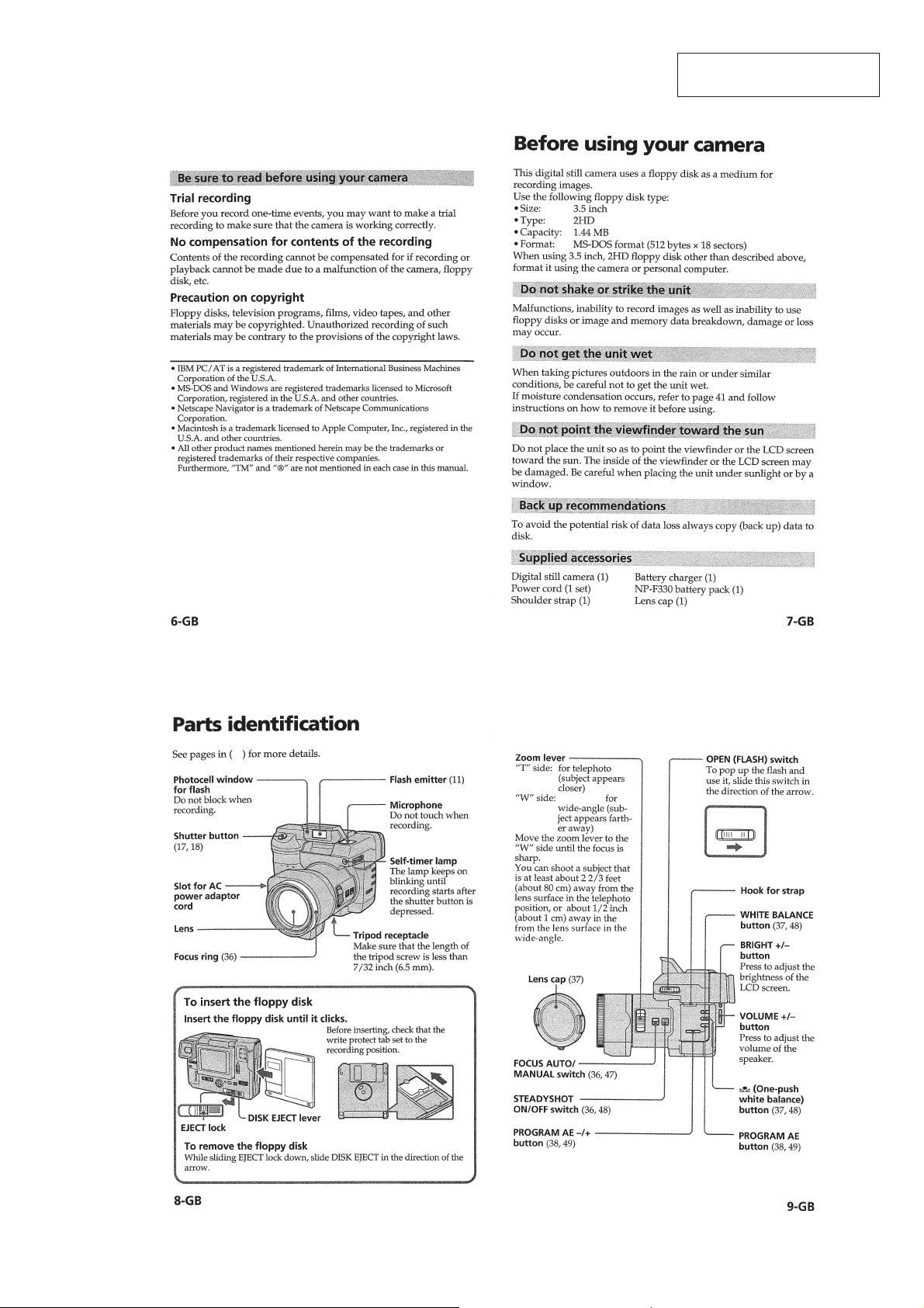
Before using your camera..........................................................1-1
Parts identification..................................................................... 1-1
Basic operations
Preparation .............................................................................1-2
1: Charging the battery pack..................................................1-2
2: Installing the battery pack..................................................1-2
3: Setting the date and time ...................................................1-3
Recording and playing back images ......................................1-3
1: Recording still images .......................................................1-3
2: Recording moving images .................................................1-4
3: Playing back still images ...................................................1-4
4: Playing back moving images .............................................1-4
Battery life/No. of images that can be recorded/
played back ............................................................................1-5
Viewing images using a personal computer ..........................1-5
Advanced operations
Changing the mode settings...................................................1-6
Setting the mode of each item ............................................... 1-6
Using various functions for recording ...................................1-8
Focusing manually................................................................. 1-8
Releasing the Steady Shot function .......................................1-8
Adjusting the white balance...................................................1-8
Using the PROGRAM AE function .......................................1-9
Additional information
Charging the lithium battery in the camera ...........................1-9
Precautions.............................................................................1-9
Troubleshooting ...................................................................1-10
Self-diagnosis display ..........................................................1-10
Warning messages ...............................................................1-10
Function guide .....................................................................1-11
2. DISASSEMBLY
2-1. EVF Block (1), RL-52 Board ..........................................2-1
2-2. EVF Block (2) .................................................................2-2
2-3. VF-131 Board..................................................................2-2
2-4. Cabinet (ST) Assembly, FLASH Unit, MA-348 Board ..2-3
2-5. LCD Unit, PD-104 Board................................................2-3
2-6. Lens Block.......................................................................2-4
2-7. CD-207 Board, VP-49 Board, SE-78 Board ...................2-5
2-8. FC-67 Board, DD-119 Board ..........................................2-6
2-9. PK-45 Board, FDD Block Assembly ..............................2-7
2-10. Circuit Boards Location ..................................................2-8
2-11. Flexible Boards Location ................................................2-8
3. BLOCK DIAGRAMS
3-1. Overall Block Diagram ...................................................3-1
3-2. Camera/FDD Interface Block Diagram........................... 3-5
3-3. Mode Control Block Diagram .........................................3-9
3-4. LCD Block Diagram .....................................................3-13
3-5. Color EVF Block Diagram............................................3-15
3-6. Power Block Diagram ...................................................3-18
4. PRINTED WIRING BOARDS AND
SCHEMATIC DIAGRAMS
4-1. Frame Schematic Diagram ..............................................4-1
4-2. Printed Wiring Boards and Schematic Diagrams ............4-6
• CD-207 (CCD Imager)
Printed Wiring Board ......................................4-7
• CD-207 (CCD Imager)
Schematic Diagram .........................................4-8
• SE-78 (YAW, Pitch Sensor)
Printed Wiring Board and
Schematic Diagram .........................................4-9
• VP-49 (Steady Shot Control)
Schematic Diagram .......................................4-12
• VP-49 (Steady Shot Control, Active Prism Actuator
Drive) Printed Wiring Board.......................................4-15
• FC-67 (Camera Y/C Process, DRAM Control,
Lens Motor Drive, D/A Converter, Audio A/D.D/A
Converter, FD/System Control, HI Control)
Printed Wiring Board ....................................4-17
• FC-67 (Camera Y/C Process)(1/7)
Schematic Diagram .......................................4-22
• FC-67 (DRAM Control)(2/7)
Schematic Diagram .......................................4-25
• FC-67 (Lens Motor Drive)(3/7)
Schematic Diagram .......................................4-29
• FC-67 (D/A Converter)(4/7)
Schematic Diagram .......................................4-31
• FC-67 (Audio D/A.A/D Converter)(5/7)
Schematic Diagram .......................................4-35
• FC-67 (FD/System Control)(6/7)
Schematic Diagram .......................................4-37
• RL-52 (Release Switch)
Printed Wiring Board ....................................4-41
• FC-67 (HI Control)(7/7)
Schematic Diagram .......................................4-42
• PK-45 (REC/PB AMP, Motor Drive)(1/4)
Schematic Diagram .......................................4-45
• PK-45 (LCD Drive)(2/4)
Schematic Diagram .......................................4-49
• PK-45 (Timing Generator)(3/4)
Schematic Diagram .......................................4-51
• PK-45 (Mode Switch)(4/4)
Schematic Diagram .......................................4-55
• PK-45 (REC/PB AMP, Motor Drive, LCD Drive,
Timing Generator, Mode Switch)
Printed Wiring Board ....................................4-57
• PD-104 (Back-Light Drive)
Printed Wiring Board and
Schematic Diagram .......................................4-62
• MA-348 (MIC AMP, ALC)
Printed Wiring Board and
Schematic Diagram .......................................4-65
• VF-131 (LCD Drive, Timing Generator)
Printed Wiring Board ....................................4-69
• VF-131 (LCD Drive, Timing Generator)(1/2)(2/2)
Schematic Diagram .......................................4-71
• DD-119 (DC/DC Converter)
Schematic Diagram .......................................4-75
• DD-119 (DC/DC Converter)
Printed Wiring Board ....................................4-79
• MF Block, ZM Block, SW Block
Schematic Diagram .......................................4-82
5. ADJUSTMENTS
5-1. Camera Section Adjustment ............................................5-1
1-1. Preparations before Adjustment (Camera Section) ......... 5-1
1-1-1.List of Service Tools........................................................5-1
1-1-2.Preparations .....................................................................5-2
1-1-3.Discharging of the flashlight power supply.....................5-2
1-1-4.Precaution ........................................................................5-4
1. Setting the Switch............................................................5-4
2. Order of Adjustments ......................................................5-4
3. Subjects ...........................................................................5-4
1-2. Initialization of F, E Page Data........................................5-5
1. Initializing the F, E Page Data .........................................5-5
2. Modification of F, E Page Data .......................................5-5
3. F Page Table ....................................................................5-5
4. E Page Table .................................................................... 5-7
— 3 —

1-3. Camera System Adjustments.........................................5-10
1. Picture Frame Setting .................................................... 5-10
2. HALL Adjustment .........................................................5-11
3. Flange Back Adjustment ...............................................5-11
4. Flange Back Check........................................................5-12
5. Light Level Adjustment .................................................5-12
6. Auto White Balance Standard Data Input ..................... 5-13
7. Auto White Balance Adjustment ................................... 5-13
8. Color Reproduction Adjustment....................................5-14
9. White Balance Check .................................................... 5-15
10. Strobe Light Level Adjustment .....................................5-15
11. Strobe White Balance Adjustment.................................5-16
12. Strobe Light Level and White Balance Check ..............5-16
13. Steady Shot Adjustment ................................................5-17
13-1. Steady Shot Adjustment (1)........................................... 5-17
13-2. Steady Shot Adjustment (2)........................................... 5-18
14. CCD Defect Compensation ...........................................5-19
14. CCD Defect Compensation Check................................5-19
1-4. Color Electronic Viewfinder System Adjustment..........5-20
1. EVF Initial Data Input ...................................................5-20
2. VCO Adjustment (VF-131 board).................................5-21
3. Bright Adjustment (VF-131 board) ...............................5-21
4. Contrast Adjustment (VF-131 board) ............................5-22
5. Backlight Consumption Current Adjustment
(VF-131 board)..............................................................5-22
6. White Balance Adjustment (VF-131 Board) .................5-23
1-5. LCD System Adjustment...............................................5-24
1. LCD Initial Data Input ..................................................5-24
2. VCO Adjustment (PK-45 board) ...................................5-25
3. D range Adjustment (PK-45 board)...............................5-25
4. Bright Adjustment (PK-45 board).................................5-26
5. Contrast Adjustment (PK-45 board) ..............................5-26
6. Color Adjustment (PK-45 board) ..................................5-27
7. V-COM Level Adjustment (PK-45 board) .................... 5-27
8. V-COM Adjustment (PK-45 board) ..............................5-28
9. White Balance Adjustment (PK-45 board)....................5-28
1-6. System Control System Adjustment..............................5-29
1. Battery End Adjustment (FC-67 board) ........................ 5-29
2. Alignment Check (FDD Unit) .......................................5-30
5-2. Service Mode.................................................................5-31
2-1. Adjustment Remote Commander ..................................5-31
1. Using the Adjustment Remote Commander..................5-31
2. Precautions upon using the adjustment remote
commander ....................................................................5-31
2-2. Data Process ..................................................................5-32
2-3. Service Mode.................................................................5-33
1. Setting the Test Mode ....................................................5-33
2. Bit value discrimination ................................................5-33
3. Switch Check (1) ...........................................................5-33
4. Switch Check (2) ...........................................................5-34
5. Self Diagnosis Log Check.............................................5-34
6. REPAIR PARTS LIST
6-1. Exploded Vie ws ...............................................................6-1
6-1-1.Cabinet (RL) Section.......................................................6-1
6-1-2.EVF Section ....................................................................6-2
6-1-3.Cabinet (Front) Section ...................................................6-3
6-1-4.Cabinet (Rear) Section ....................................................6-4
6-1-5.LCD Panel Section ..........................................................6-5
6-1-6.Lens Block Section.......................................................... 6-6
6-2. Electrical Parts List ......................................................... 6-7
* The color reproduction frame is shown on page 185.
— 4 —
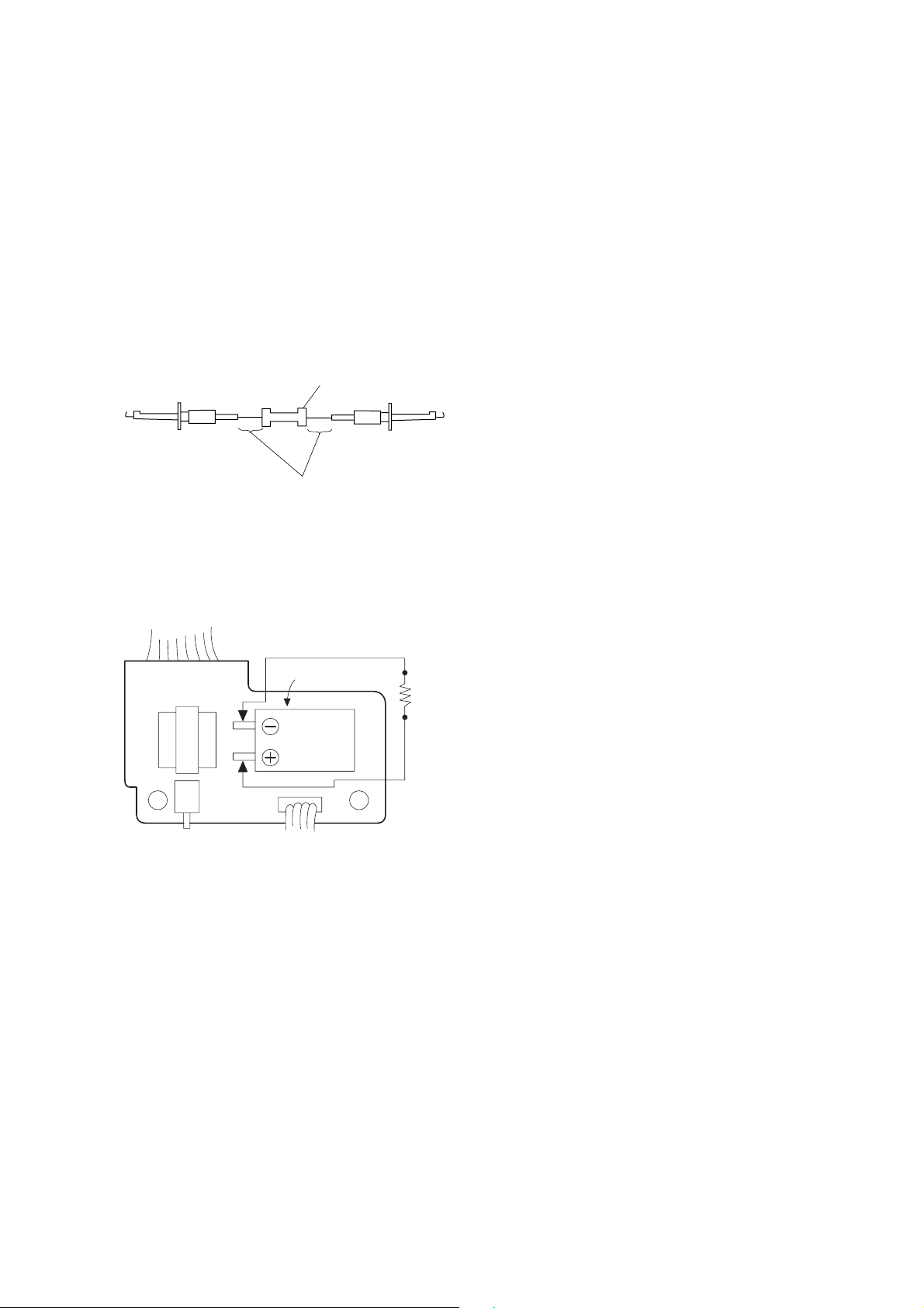
SERVICE NOTE
[Discharging of the FLASH unit’s charging capacitor]
The charging capacitor of the FLASH unit is charged up to the
maximum 300 V potential.
There is a danger of electric shock by this high voltage when the
battery is handled by hand. The electric shock is caused by the
charged voltage which is kept without discharging when the main
power of the MVC-FD91 is simply turned off. Therefore, the
remaining voltage must be discharged as described below.
Preparing the Short Jig
To preparing the short jig. a small clip is attached to each end of a
resistor of 1kΩ /1W (1-215-869-11)
Wrap insulating tape fully around the leads of the resistor to prevent
electrical shock.
1kΩ/1W
Wrap insulating tape.
Discharging the Capacitor
Short circuits between the positive and the negative terminals of
charged capacitor with the short jig about 10 seconds.
Capacitor
Short jig
FLASH UNIT
— 5 —
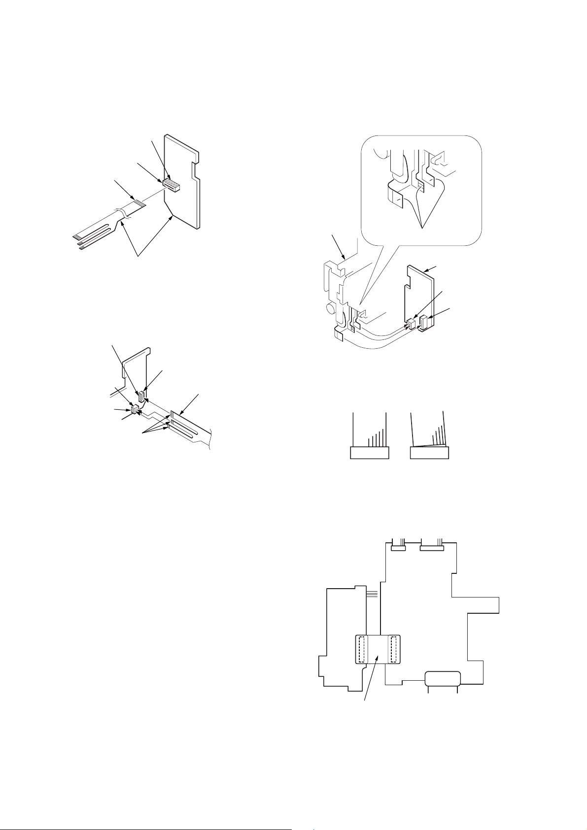
[How to connect the extension cable]
e
1. Connection between the FDD unit and PK-45 board.
1) Connection of the extension cable (J-6082-427-A)
Conductor side
CN013
Conductor side
Extension cable
(J-6082-427-A)
Fig.1
2) Connection between the PK-45 board and extension cable
Conductor side
CN601
CN602
For both two cables,
the conductor points
are on this side.
Conductor side
Extension cable
(J-6082-427-A)
3) Connection between the FDD unit and extension cable
FDD unit
Conductor side
Extension cabl
(J-6082-427-A)
CN011
CN012
Fig.3
Note : The floppy disk drive and PK-45 board could be destroyed unless
the flexible board is connected normally to the connector.
(See Fig. 4.)
Fig.2
Good NG
Fig.4
2. Connection between the DD-119 board and FC-67
board
FC-67
DD-119
board
CN303
Extension cable (50P)
(J-6082-434-A)
board
CN603
Fig.5
— 6 —

[Description on Self-diagnosis Display]
Self-diagnosis display
• C: ππ: ππ
The contents which can be handled
by customer, are displayed.
• E: ππ: ππ
The contents which can be handled
by engineer, are displayed.
Note : The “Self-diagnosis” data is backed up by the coin lithium
battery.The data will be lost and initialized when the coin lithium
battery is removed.
Display Code
C:32:01
C:13:01
E:91:01
E:61:00
E:61:10
Countermeasure
Change the disk and turn off the main
power then back on.
Replace the floppy disk.
Format the floppy disk with the MVCFD91.
Checking of flash unit or replacement of
flash unit
Checking of lens drive circuit
Cause
Defective floppy disk.
• The type of floppy disk that cannot be
used by this machine, is inserted.
(Such as 2DD)
• Data is damaged.
• Unformatted disk is inserted.
Abnormality when flash is being
charged.
When failed in the focus initialization.
Caution Display During Error
DRIVE ERROR
DISK ERROR
Flash LED
Flash display
Flashing at 3.2 Hz
—
— 7 —
SECTION 1
GENERAL
MVC-FD91
This section is extracted from
instruction manual.
1-1
1-2
1-3
1-4
1-5
1-6
1-7
1-8
1-9
1-10
1-11E
SECTION 2
DISASSEMBLY
NOTE: Follow the disassembly procedure as shown in the flow chart below.
MVC-FD91
LCD unit,
2-5.
PD-104 board
EVF block (1),
2-1. 2-2.
RL-52 board
Cabinet (ST) assembly,
2-4.
FLASH unit, MA-348 board
2-6.
LENS block
MVC-FD91 MAVICA
CD-207 board, VP-49 board,
2-7.
SE-78 board
2-8.
FC-67 board, DD-119 board
2-9.
PK-45 board,
FDD block assembly
EVF block (2)
2-3.
VF-131 board
NOTE: Follow the disassembly procedure in the numerical order given.
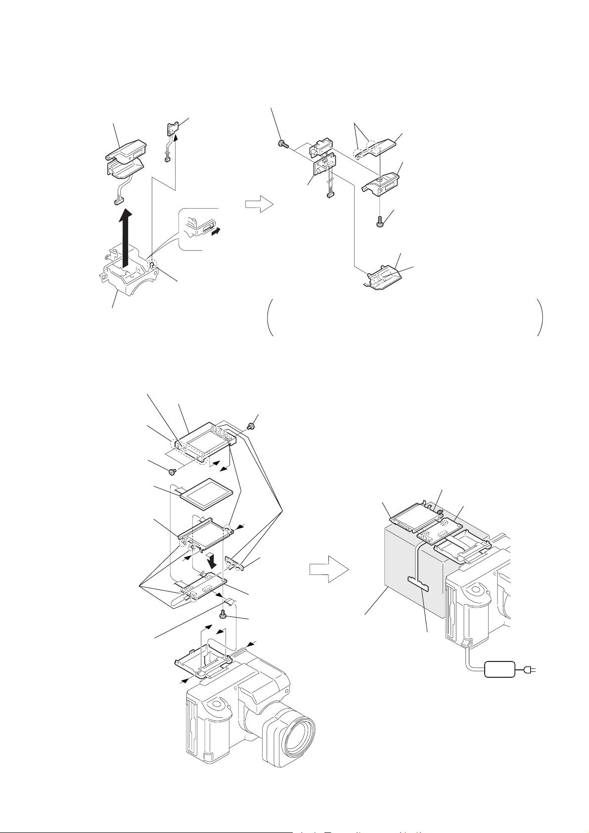
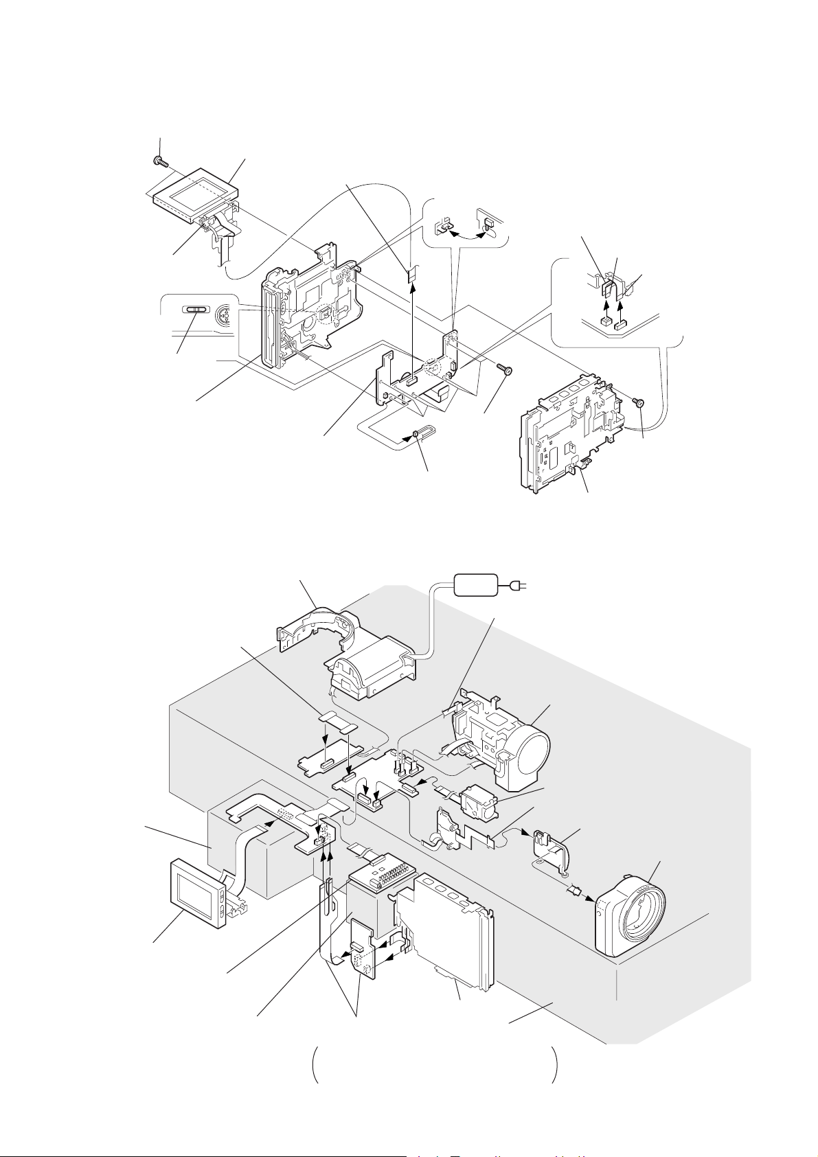
2-1. EVF BLOCK (1), RL-52 BOARD
LCD check
Service position
EVF check
Service position
FLASH UNIT
replacement
LENS unit check
Service position
MAIN (FC-67) board check
Service position
Overall check
Service position
!¢
Cabinet (EVF) assembly
0
Screw (M2 × 4),
lock ace, P2
1
lock ace, P2
In case of removing
the RL-52 board
RL-52 board
!∞
EVF block
Remove the FP-68 flexible board
from the cabinet (ST) assembly
with care so that the board must
not be caught.
!£
Remove
the claws
Cabinet (ST)
assembly
(See page 2-3)
Two screws (M2 × 4),
5
Shaft (POP)
a
4
Cabinet (microphone) assembly
a
8
Screw (M2 × 4)
7
Open the flash lid.
!™
Screw (M1.7)
8
lock ace, P2
6
Pull the knob
in the direction
of the arrow.
8
Screw (M2 × 4)
!¡
FP-68 flexible
board (21P)
Screw (M2 × 4),
Claws
3
Cabinet (RL) assembly
2
Tapping screw (B2 × 5)
9
Pull up the LCD block assembly
2-1
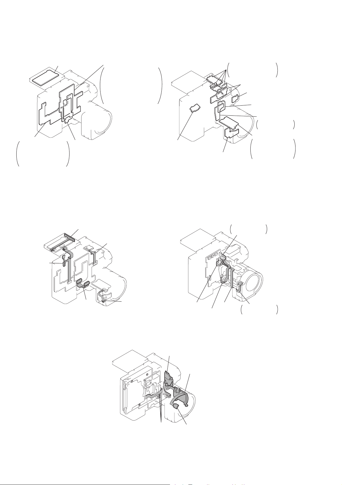
2-2. EVF BLOCK (2)
)
1
Remove the claws
2
VF-131 board (1)
7
Lens holder
assembly
5
VF-131 board (2)
4
Remove
the claws
3
Cover the cushion and diffusion plate
with a piece of paper and adhesive
tape or the like so that the parts must
not be scattered.
[EVF CHECK SERVICE POSITION]
6
VF-131 board (3)
Base
(Use box or the like.)
VF-131 board
FP-68 flexible board
CN601 21P (FC-63 board)
Conductor side
2-3. VF-131 BOARD
9
LENS holder assembly
Shining surface
Rough surface
Shining surface
6
1
LCD cushion (3)
2
BL illuminator
3
LCD cushion
7
LCD
LCD flexible (16P)
5
Remove the claws
8
VF-131 board
4
FP-68 flexible board (21P
AC
ADAPTOR
AC IN
2-2
2-4. CABINET (ST) ASSEMBLY, FLASH UNIT, MA-348 BOARD
!£
FLASH unit
1
Remove the claw
3
Slide the knob in the
direction of the arrow
a
to raise the flash
unit.
Note : Before starting to disassemble, confirm how harnesses are routed.
When re-assembling the parts, route the harnesses in the original
position. If the harnesses are not routed corrected, it can break down
the harnesses when the Cabinet (ST) assembly is re-assembled.
2
MA-348 board
(Note)
4
Cabinet (upper) (POP)
assembly
5
Cabinet (ST) assembly
6
Two tapping screws (B2 × 5)
7
Remove the claw
8
ST blind cabinet
9
Tapping screw (B2 × 5)
!º
Remove the claws
!¡
Cabinet (upper) (POP)
!™
Cabinet (lower) (POP) assembly
a
a
c
d
a
b
d
c
b
PD-104
0
Slide the board
in the direction
of the arrow
e
to disengage the
claws.
1
Screws (M1.4)
2
Screws (M1.4)
When re-assembling
put in the LCD this
side before.
5
Screw (M2 × 3)
6
Remove
the claws
3
Remove the claw
7
FP-70 flexible
FP-70 flexible
4
Remove the FP-69 flexible
8
P cabinet (front) assembly
9
Remove
the claws
!¡
LCD
!™
Cold cathode
florescent tube
!£
PD-104 board
e
Back light
(Cold cathode florescent tube)
PD-104 board
LCD
AC IN
AC
ADAPTOR
Base
(Use box or the like.)
2-5. LCD UNIT, PD-104 BOARD
[LCD CHECK SERVICE POSITION]
2-3
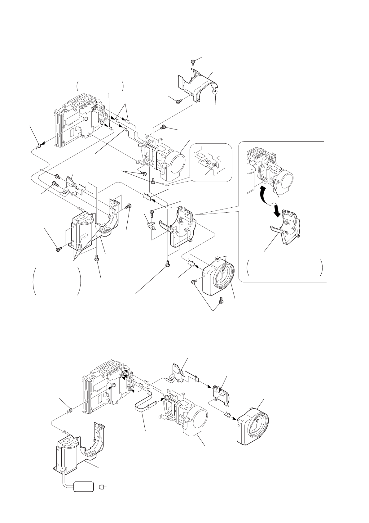
2-6. LENS BLOCK
!•
Cable (4P)
@º
Screw
(M2
×
3)
@¡
Tapping screw
(B2
×
5)
!¢
Two screws (M2 × 4),
lock ace, P2
!¶
Remove the claws
Remove the claws
gradually because
the flexible wire
can be cut if it is
removed at once.
@™
SW block
(side sw)
!ª
SW block (side sw)
flexible board (10P)
Be careful that the
board is very short.
FC-67
DD-119
@¶
FP-67 flexible
board (16P)
@∞
Screws
(M2
×
3)
!§
(M2
lock ace, P2
@£
Cabinet (front)
assembly
!∞
Two screws (M2 × 4),
lock ace, P2
!™
lock ace, P2
6
Screw (M2 × 4),
lock ace, P2
@§
Flexible board
(from lens block)
!¡
Plate (A)
fixed
Two screws
×
4),
3
ZM block
flexible board
Screws (M2 × 4),
5
@¢
Screw (M2 × 3)
@•
Lens block assembly
Screw
9
SW block (side sw)
flexible board
0
Tapping screw
(B2
×
5)
Screw (M2 × 3)
8
Cabinet (LT)
7
Remove the claw
2
Remove
the claws
4
Cabinet (VP) assembly
Be careful that it can
be easily caught.
a
!£
Cabinet (LB) assembly
Remove gently the cabinet (LB)
assembly in the direction of the
a
arrow
.
[LENS BLOCK CHECK SERVICE POSITION]
FC-67
Battery cable (4P)
CN301 (DD-119 board)
ADAPTOR
Cabinet (front) assembly
AC
DD-119
Extension cable
(J-6082-357-A)
AC IN
1
Screws (M2 × 4), lock ace, P2
SW block (side sw)
LENS block
ZM block (front sw)
Cabinet (VP) assembly
2-4
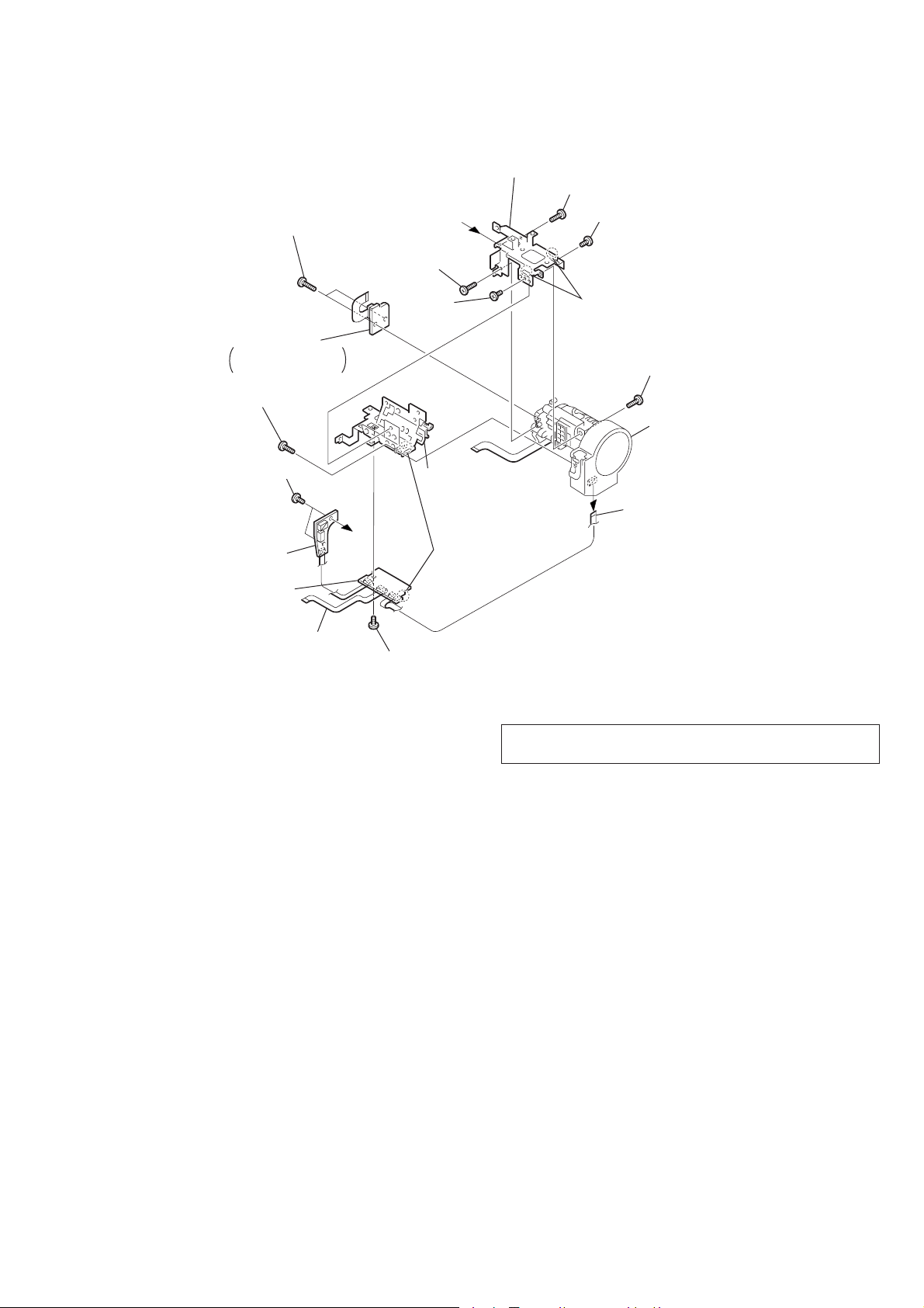
2-7. CD-207 BOARD, VP-49 BOARD, SE-78 BOARD
2
!∞
LENS flame (upper)
1
Tite (2), +B Tapping (P)
2
CD-207 board
Remove soldering
of the CCD imager.
!§
Tapping screw (B2 × 5)
3
Screws (M2 × 3)
4
SE-78 board
8
VP-49 board
9
(B2 × 5)
a
VP-49
Tapping screw
!º
(M2 × 3)
a
Screw
!¶
LENS frame (lower)
assembly
7
Remove the claws
!¡
Tapping screw (B2 × 5)
!™
Screw (M2 × 3)
!¢
Remove the claws
!£
Screw (M1.7), 0-No. +P
!•
LENS assembly
5
FP-71 flexible board (13P)
FP-73
6
Screw (M2 × 3)
Be sure to read “Note on the CCD imager replacement” on
page 4-8 when changing the CCD Imager.
2-5
2-8. FC-67 BOARD, DD-119 BOARD
6
a
[MAIN (FC-67) BOARD CHECK SERVICE POSITION]
Remove the claws
7
FC-67 board
Slide it in the direction of the
arrow
FC-67
Board
2
Board to board connector (50P)
4
FP-65 flexible board (70P)
a
, then remove it.
5
Screws (M2 × 3)
3
DD-119 (110) board
DD-119
1
Screws (M2 × 3)
Extension cable
(J-6082-434-A)
Cabinet (front) assembly
DD-119
FC-67
FP-65 flexible board
AC
ADAPTOR
AC IN
Extension cable (J-6082-357-A)
Lens block
SW block (side sw)
ZM block (front sw)
Cabinet (VP) assembly
CPC-12 jig (J-6082-436-A)
Base
(Use box or the like.)
2-6
2-9. PK-45 BOARD, FDD BLOCK ASSEMBLY
!º
Two tapping screws (B2 × 5)
!¡
LCD block assembly
7
FP-69 flexible board (28P)
S691
(PANEL REV)
When re-assembling
set this knob the center
!™
Cabinet (rear) assembly
9
PK-45 board
PK-45
Board
6
8
Eight tapping
screws (B2 × 5)
Cable (2P)
3
FDD flexible board (side 1) (5P)
2
FDD flexible board (side 0) (5P)
1
FDD flexible board (18P)
4
Screw (M2 × 3)
5
FDD block assembly
[OVERALL CHECK SERVICE POSITION]
Cabinet (front) assembly
Extension cable
(J-6082-434-A)
DD-119
Base
(Use box or the like.)
PK-45
FC-67
AC
ADAPTOR
AC IN
Extension cable (J-6082-357-A)
Lens block
EVF block
SW block (side sw)
ZM block (front sw)
Cabinet (VP) assembly
LCD block assembly
CPC-12 jig
(J-6082-436-A)
Base
(Use box or the like.)
FDD block assembly
Extension cable
(J-6082-427-A)
Base
(Use box or the like.)
Note : When connecting the extension cable,
refer to “1. Connection between the FDD
unit and PK-45 board” of page 6.
2-7
)
2-10.CIRCUIT BOARDS LOCATION
PD-104
(BACK LIGHT DRIVE)
PK-45
REC PB AMP,
MOTOR DRIVE,
LCD DRIVE,
TIMING GENERATOR,
MODE SWITCH
DD-119 (110)
(DC/DC CONVERTER)
FC-67
CAMERA Y/C PROCESS,
DRAM CONTROL, LENS
MOTOR DRIVE, D/A
CONVERTER, AUDIO
A/D.D/A CONVERTER,
FD/SYSTEM CONTROL,
HI CONTROL
2-1 1.FLEXIBLE BOARDS LOCATION
RL-52
(RELEASE SWITCH)
CS UNIT (Included VAP UNIT)
(STEADY SHOT DRIVE)
VF-131
LCD DRIVE,
TIMING GENERATOR,
BACK LIGHT DRIVE
FLASH UNIT
MA-348
(MIC AMP, ALC)
CD-207
(CCD IMAGER)
SE-78
YAW,
PITCH SENSOR
VP-49
STEADY SHOT
CONTROL,
ACTIVE PRISM
ACTUATOR DRIVE
FP-69
FP-70
(BRIGHT/VOLUME)
FP-68
FP-65
FP-71
SW block
(SIDE SW)
FP-67
ZM block
(FRONT SW
FP-72
FP-73
FROM FOCUS/
ZOOM MOTOR
FROM STEADY
SHOT MOTOR
(FROM FDD)
MF block
2-8E
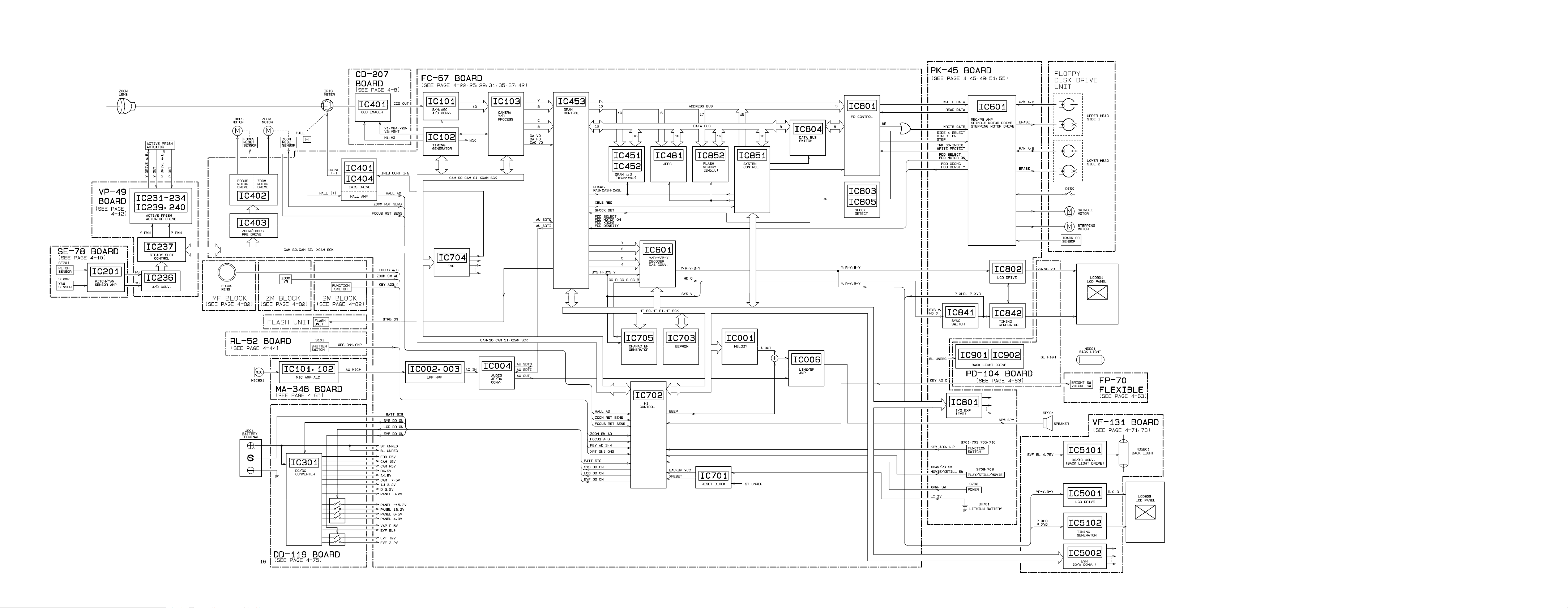
3-1. OVERALL BLOCK DIAGRAM
SECTION 3
BLOCK DIAGRAMS
MVC-FD91
MVC-FD91
3-1 3-2 3-3
MVC-FD91
3-2. CAMERA/FDD INTERFACE BLOCK DIAGRAM
IC401 2,4
IC401 8
IC101 @§ CAMERA REC
IC101 2 – !¡
CAMERA REC/PB
IC103 #§,$∞
CAMERA REC/PB
78µsec
IC401 !¢
60nsec
IC401 1,3
IC401 !∞,!§
60nsec
78µsec
7.5Vp-p
3Vp-p
8Vp-p
5Vp-p
78µsec
1.8Vp-p
IC102 $º,$¡
CAMERA REC
78µsec
IC102 $™,$¢
CAMERA REC
IC102 !™,!£
CAMERA REC
60nsec
IC102 9
CAMERA REC
60nsec
78µsec
8Vp-p
7.5Vp-p
3Vp-p
4Vp-p
IC102 4
CAMERA REC/PB
30nsec
IC102 @∞
CAMERA REC/PB
60nsec
3.8Vp-p
4.0Vp-p
78µsec
1.4Vp-p
IC101 !§
CAMERA REC/PB
60nsec
4.0Vp-p
60nsec
3.1Vp-p
60nsec
3.8Vp-p
IC801 *£
16.26MHz
5.0Vp-p
IC601 $™
CAMERA REC/PB
IC601 !ª
IC601 @£
IC601 !¢
IC601 $¶
78µsec
78nsec
78µsec
78µsec
0.16Vp-p
0.18Vp-p
0.1Vp-p
3.3Vp-p
IC601 $§
20msec
3.3Vp-p
IC601 5
60nsec
3.8Vp-p
IC601 #¶
60nsec
3.8Vp-p
IC851 *º
7.41MHz
2.0Vp-p
4.0MHz
3.2Vp-p
3-5 3-6 3-7 3-8
3-3. MODE CONTROL BLOCK DIAGRAM
MVC-FD91
IC702 $º
IC237 @¢
12MHz
2.8Vp-p
IC702 %£
20MHz
32.768kHz
3.8Vp-p
3.4Vp-p
3-9 3-10 3-11
MVC-FD91
MVC-FD91
3-4. LCD BLOCK DIAGRAM
IC802 8
78µsec
0.3Vp-p
IC802 @º
156µsec
4Vp-p
IC802 @™
156µsec
4Vp-p
IC802 @¢
156µsec
4Vp-p
IC901 1
CAMERA REC/PB
2µsec
5Vp-p
IC802 9
IC802 !º
IC841 4
78µsec
78µsec
20msec
0.45Vp-p
0.25Vp-p
3.3Vp-p
IC841 1
78µsec
3.3Vp-p
IC842 @§
150nsec
4.5Vp-p
IC802 @•,@ª
IC842 #¶
1.5msec
78µsec
3.2Vp-p
IC843 7
4.5Vp-p
156µsec
3.3Vp-p
3-13 3-14

3-5. COLOR EVF BLOCK DIAGRAM
IC5001 9
MVC-FD91
MVC-FD91
IC5001 8
IC5001 !º
IC5001 @º
0.35Vp-p
H
2H
H
0.35Vp-p
7.6Vp-p
IC5001 @™
2H
7.6Vp-p
IC5001 @¢
7.6Vp-p
2H
IC5101 !∞
78µsec
14.0Vp-p
IC5102 #∞
IC5102 $∞
0.2Vp-p
H
3.2Vp-p
H
IC5102 @¶
3.2Vp-p
V
3.2Vp-p
H
IC5102 $¡
16.4MHz
2.5Vp-p
3-15 3-16 3-17

MVC-FD91
3-6. POWER BLOCK DIAGRAM
IC301 $§
2.1µsec
IC301 $¢
2.2µsec
2.0Vp-p
0.8Vp-p
3-18 3-19 3-20E

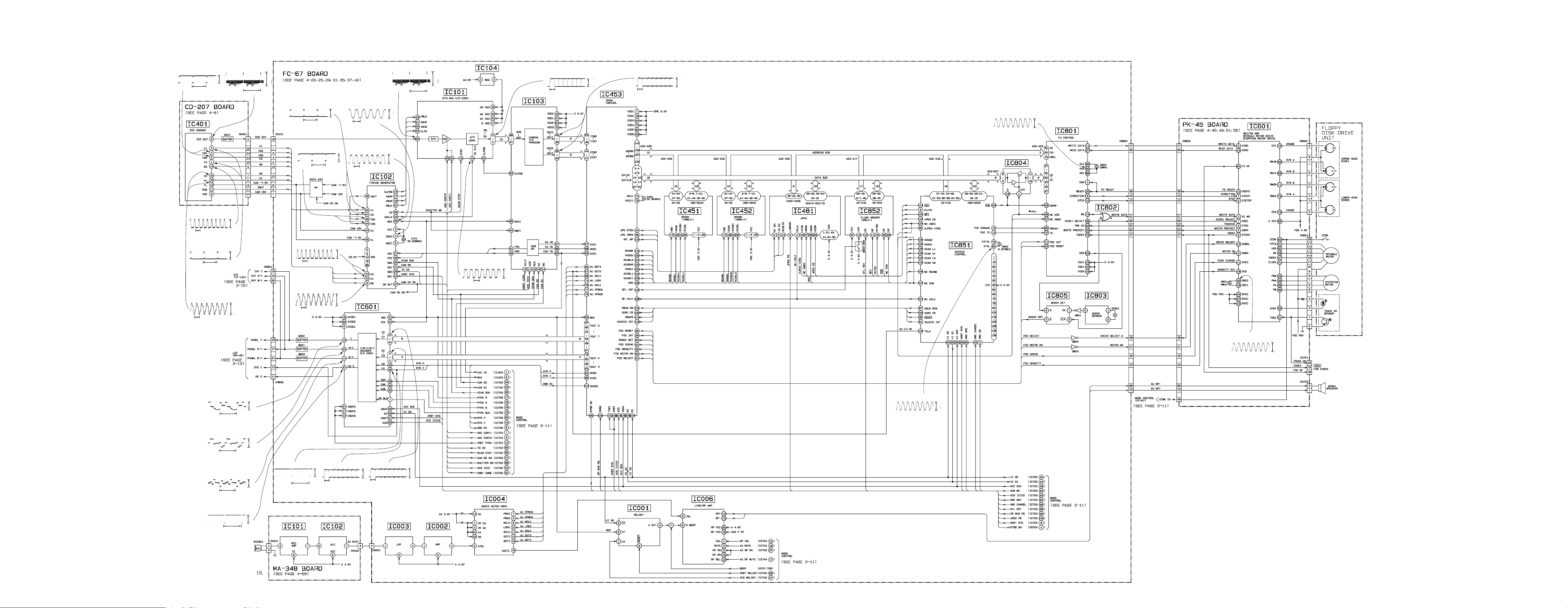
PRINTED WIRING BOARDS AND SCHEMATIC DIAGRAMS
4-1. FRAME SCHEMATIC DIAGRAM
SECTION 4
MVC-FD91
4-1 4-2 4-3
4-4
FRAME SCHEMATIC DIAGRAM

MVC-FD91
MVC-FD91
4-2. PRINTED WIRING BOARDS AND SCHEMATIC DIAGRAMS
THIS NOTE IS COMMON FOR WIRING BOARDS AND SCHEMATIC DIAGRAMS
(In addition to this, the necessary note is printed in each block)
(For printed wiring boards)
• b: Pattern from the side which enables seeing.
(The other layers' patterns are not indicated.)
• Through hole is omitted.
• Circled numbers refer to waveforms.
• There are few cases that the part printed on diagram
isn’t mounted in this model.
• Chip parts.
Transistor Diode
C
5
BE
64
2
13
5
46
2
31
45
2
31
12
4
53
3
21321321
(For schematic diagrams)
• All capacitors are in µF unless otherwise noted. pF : µµF.
50V or less are not indicated except for electrolytics and
tantalums.
• Chip resistors are 1/10W unless otherwise noted.
kΩ=1000Ω, MΩ=1000kΩ.
• Caution when replacing chip parts.
New parts must be attached after removal of chip.
Be careful not to heat the minus side of tantalum capacitor, Because it is damaged by the heat.
• Some chip part will be indicated as follows.
Example C541 L452
22U 10UH
TA A 2520
(Measuring conditions voltage and waveform)
• Voltages and waveforms are measured between the measurement points and ground when camera shoots color bar chart of
pattern box. They are reference values and reference waveforms. *
(VOM of DC 10 MW input impedance is used.).
• Voltage values change depending upon input impedance of VOM
used.) *
1. Connection
Pattern box
Front of the protection glass
1.5m
CD-207 BOARD
C401 A-4
C402 B-4
C403 A-4
C404 B-4
C405 A-4
C406 A-4
CN401 B-4
IC401 A-1
L401 B-4
Q401 B-4
R401 B-4
R402 B-4
R403 B-4
R404 A-4
R405 A-3
R406 B-4
CD-207 (CCD IMAGER) PRINTED WIRING BOARD
— Ref. No. CD-207 Board; 2,000 Series —
CD-207
CAMERA REC
1
IC401 1,3
78µsec
2
IC401 2,4
78µsec
3
IC401 8
4
IC401 !∞,!§
BOARD
8Vp-p
7.5Vp-p
1.8Vp-p
78µsec
Kinds of capacitor
Temperature characteristics
External dimensions (mm)
• Constants of resistors, capacitors, ICs and etc with XX indicate
that they are not used.
In such cases, the unused circuits may be indicated.
• Parts with ★ differ according to the model/destination.
Refer to the mount table for each function.
• All variable and adjustable resistors have characteristic curve
B, unless otherwise noted.
• Signal name
XEDIT→ EDIT PB/XREC → PB/REC
• 2 : non flammable resistor
• 1 : fusible resistor
• C : panel designation
• A : B+ Line *
• B : B– Line *
• J : IN/OUT direction of (+,–) B LINE. *
• C : adjustment for repair. *
• Circled numbers refer to waveforms. *
*Indicated by the color red.
Note :
The components identified by
mark ! or dotted line with mark
! are critical for safety.
Replace only with part number
specified.
Note :
Les composants identifiés par
une marque ! sont critiques
pour la sécurité.
Ne les remplacer que par une
pièce portant le numéro spécifié.
2. Adjust the distance so that the output waveform of Fig. a and
the Fig. b can be obtain.
A=B
A
B
C=D
C
H
D
H
Fig. a (CPC-12 jig TP-VG output waveform)
Electron beam
scanned frame
Yellow
Cyan
White
Green
Red
Blue
Magenta
LCD picture frame
Fig.b (Picture on LCD)
When indicating parts by reference number, pleas include
the board name.
For printed wiring boards
• This board is six-layer print board. However, the patterns of layers two to five have not been included in
the diagram.
• Chip parts
Transistor
C
BE
There are few cases that the part printed on this
diagram isn’t mounted in this model.
RL-52
(RELEASE SWITCH)
CS UNIT (Included VAP UNIT)
(STEADY SHOT DRIVE)
VF-131
LCD DRIVE,
TIMING GENERATOR,
BACK LIGHT DRIVE
FLASH UNIT
MA-348
(MIC AMP, ALC)
CD-207
(CCD IMAGER)
SE-78
YAW,
PITCH SENSOR
VP-49
STEADY SHOT
CONTROL,
ACTIVE PRISM
ACTUATOR DRIVE
60nsec
5
60nsec
5Vp-p
IC401 !¢
3Vp-p
4-6
CCD IMAGER
CD-207
4-7 4-8

SE-78 (YAW, PITCH SENSOR) PRINTED WIRING BOARD
— Ref. No. SE-78 Board; 1,000 Series —
SE-78 BOARD
C201 C-5
C202 B-6
C203 C-5
C204 A-5
C205 B-2
C206 B-1
C207 B-5
C208 C-5
C209 B-5
C210 C-5
C211 A-1
C212 C-2
C213 B-5
C214 C-5
C215 B-6
C216 B-6
CN201 A-5
IC201 B-5
L201 B-6
R201 C-5
R202 B-5
R203 B-5
R204 C-5
R205 B-1
R206 B-5
R207 B-5
R208 C-5
R209 C-5
R210 B-5
R211 C-5
SE201 C-1
SE202 B-1
MVC-FD91
For printed wiring boards
• This board is six-layer print board. However, the patterns of layers two to five have not been included in
the diagram.
There are few cases that the part printed on this
diagram isn’t mounted in this model.
VF-131
LCD DRIVE,
TIMING GENERATOR,
BACK LIGHT DRIVE
FLASH UNIT
MA-348
(MIC AMP, ALC)
CD-207
(CCD IMAGER)
SE-78
YAW,
PITCH SENSOR
VP-49
RL-52
(RELEASE SWITCH)
CS UNIT (Included VAP UNIT)
(STEADY SHOT DRIVE)
STEADY SHOT
CONTROL,
ACTIVE PRISM
ACTUATOR DRIVE
4-9 4-10 4-11
YAW, PITCH SENSOR
SE-78

MVC-FD91
VP-49
1
IC237 @¢
12MHz
BOARD
2.8Vp-p
STEADY SHOT CONTROL
VP-49
4-12 4-13 4-14

VP-49 (STEADY SHOT CONTROL, ACTIVE PRISM ACTUATOR DRIVE) PRINTED WIRING BOARD
— Ref. No. VP-49 Board; 2,000 Series —
VP-49 BOARD
C231 C-4
C232 C-4
C234 D-2
C235 C-4
C236 C-3
C237 C-5
C238 C-3
C238 D-4
C239 B-2
C240 D-1
C241 D-1
C242 D-2
C243 D-2
C244 D-3
C245 D-3
C246 D-2
C247 D-3
C248 D-2
C249 D-3
C250 E-3
C251 D-3
C252 E-3
C253 D-3
C254 D-3
C255 E-2
C257 D-2
C258 C-2
C259 C-2
C261 B-2
C262 A-2
C263 A-4
C264 D-3
CN231 B-4
CN232 B-1
CN233 B-3
FB231 A-4
IC231 C-4
IC232 C-3
IC233 A-4
IC233 D-2
IC234 D-3
IC235 E-2
IC236 C-1
IC237 A-3
IC239 E-1
IC240 E-1
L231 B-2
L232 A-2
L233 C-2
L234 B-2
L235 B-2
Q231 B-1
Q232 A-2
Q233 B-2
Q234 B-2
Q235 A-2
Q236 A-2
Q237 A-3
R231 C-3
R232 D-4
R234 D-4
R235 D-3
R235 D-4
R236 C-2
R236 C-4
R237 D-3
R239 D-4
R240 D-4
R241 C-3
R242 D-3
R243 C-3
R244 C-3
R245 D-2
R246 D-1
R247 D-2
R248 D-3
R249 D-2
R250 D-2
R251 D-3
R252 D-3
R253 D-3
R254 D-2
R255 D-2
R256 D-3
R257 E-3
R258 E-3
R259 D-3
R260 D-3
R261 E-3
R262 E-3
R263 A-1
R264 B-1
R265 A-2
R266 B-2
R267 A-2
R268 B-2
R269 B-2
R270 A-2
R271 A-2
R272 A-2
R273 A-2
R274 B-2
R275 D-2
R276 D-3
R277 B-2
R278 D-3
R279 A-4
R280 A-4
R281 A-4
R282 D-3
R283 D-3
R284 B-2
R285 B-2
R286 E-1
R287 E-1
R288 E-1
R289 E-1
R290 A-4
R291 A-2
X231 A-4
MVC-FD91
For printed wiring boards
• This board is six-layer print board. However, the patterns of layers two to five have not been included in
the diagram.
• Chip parts
Transistor
C
BE
There are few cases that the part printed on this
diagram isn’t mounted in this model.
VF-131
LCD DRIVE,
TIMING GENERATOR,
BACK LIGHT DRIVE
FLASH UNIT
MA-348
(MIC AMP, ALC)
CD-207
(CCD IMAGER)
SE-78
YAW,
PITCH SENSOR
VP-49
RL-52
(RELEASE SWITCH)
CS UNIT (Included VAP UNIT)
(STEADY SHOT DRIVE)
STEADY SHOT
CONTROL,
ACTIVE PRISM
ACTUATOR DRIVE
4-15 4-16
STEADY SHOT CONTROL
VP-49

MVC-FD91
FC-67 BOARD (SIDE A)
C001 A-3
C002 B-3
C003 A-3
C004 B-3
C005 B-2
C006 A-1
C007 A-1
C008 A-2
C009 B-2
C010 A-2
C011 A-2
C028 B-2
C029 A-2
C030 B-2
C031 B-2
C032 B-2
C037 A-2
C111 F-3
C112 F-2
C116 F-3
C117 F-3
C119 F-3
C120 F-3
C121 F-3
C122 F-3
C123 F-3
C124 F-3
C125 F-3
C126 G-2
C127 G-3
C131 F-3
C132 F-2
C135 G-2
C401 F-4
C405 G-4
C407 G-4
C409 G-4
C411 G-4
C412 G-3
C417 G-3
C701 C-2
C702 C-2
C703 B-2
C704 C-2
C705 B-2
C706 B-2
C707 B-2
C708 C-3
C709 B-3
C710 C-5
C711 C-5
C712 C-5
C713 B-5
C714 A-3
C715 A-4
C716 B-4
C717 B-4
C718 C-2
C719 C-5
C722 B-5
C724 B-2
C725 B-3
C726 B-3
C727 B-2
C728 A-5
C729 A-5
C730 B-5
C731 B-5
C732 E-4
C733 D-5
C734 D-4
C735 E-4
C736 F-4
C821 C-2
C853 D-2
C856 C-3
C858 D-4
C859 D-4
C861 D-4
C862 D-4
C865 E-2
C866 E-4
C867 C-1
C868 D-4
C869 E-4
C870 E-4
C871 E-4
C872 E-4
C873 E-4
C874 D-4
C875 D-4
CN001 G-2
CN101 F-4
CN401 G-4
CN601 E-6
CN602 A-4
CN603 C-1
CN701 F-4
CN702 G-1
CN703 A-6
CN704 G-3
D001 A-5
D002 G-4
D003 E-1
D701 C-2
D702 B-2
D703 C-2
D705 B-2
D706 E-3
FB102 F-3
FB801 C-2
FB803 C-1
IC001 A-1
IC005 A-2
IC006 A-3
IC101 F-3
IC103 F-2
IC402 G-4
IC403 G-3
IC701 C-2
IC702 C-4
IC703 C-3
IC704 E-5
IC851 D-3
IC852 D-1
L001 B-3
L002 B-3
L004 B-1
L102 G-2
L401 G-3
L402 G-3
L701 B-2
L702 E-4
L703 D-5
L802 C-2
L803 C-1
Q401 G-3
Q701 B-2
Q702 B-2
Q703 A-4
Q704 B-4
Q705 B-4
Q706 E-3
Q707 B-3
Q708 B-3
Q804 E-1
Q1005 B-1
R006 A-3
R007 A-2
R008 B-3
R009 A-1
R010 B-2
R011 A-1
R012 A-2
R013 A-2
R014 B-2
R015 B-2
R016 B-2
R018 A-2
R019 B-2
R026 B-1
R027 B-2
R028 B-1
R029 B-1
R030 A-2
R031 A-3
R032 A-2
R033 B-1
R034 B-1
R038 A-1
R041 B-1
R042 B-1
R111 F-2
R119 G-2
R122 F-3
R124 F-3
R125 F-3
R135 G-2
R136 G-2
R137 G-2
R401 F-4
R403 G-3
R404 G-3
R405 G-3
R430 G-4
R602 D-6
R603 D-6
R604 D-6
R607 D-6
R608 D-6
R609 D-6
R625 D-6
R626 D-6
R627 A-5
R628 A-5
R701 B-2
R702 B-2
R704 C-2
R705 D-4
R706 D-4
R707 C-3
R708 C-3
R709 C-3
R710 B-3
R711 B-3
R712 D-4
R713 B-3
R714 D-4
R715 C-5
R716 B-5
R717 C-4
R718 C-3
R719 A-5
R720 B-5
R721 C-4
R722 C-4
R723 C-4
R724 C-4
R725 C-4
R726 A-5
R727 A-5
R728 A-5
R729 A-5
R730 C-3
R731 B-5
R732 B-3
R733 F-4
R734 E-4
R735 B-3
R736 B-3
R737 A-5
R738 A-5
R739 A-5
R740 B-5
R741 B-5
R742 A-4
R743 B-5
R744 A-4
R745 B-5
R746 D-4
R747 B-4
R748 B-4
R749 C-2
R751 C-2
R752 A-4
R753 A-4
R754 D-4
R755 D-4
R756 F-4
R758 F-4
R759 B-2
R760 F-4
R761 B-3
R762 B-3
R763 B-3
R764 B-3
R765 B-3
R766 B-3
R769 B-3
R770 G-3
R771 G-3
R772 G-3
R773 A-4
R774 B-5
R775 C-5
R776 C-3
R777 C-3
R778 E-3
R779 A-5
R780 A-5
R781 C-2
R784 G-1
R785 G-2
R786 G-2
R824 E-4
R828 D-4
R855 E-2
R856 E-4
R857 E-4
R858 E-4
R863 D-4
R868 C-1
R871 E-4
R876 C-2
R877 C-2
R878 C-2
R879 C-3
R880 C-3
R881 C-3
R882 C-3
R883 C-3
R884 C-3
R885 E-4
R886 E-1
R888 E-4
R889 E-4
R890 E-4
R891 E-4
R892 E-3
R893 E-3
R894 E-2
R895 E-2
R896 E-4
R897 E-2
R898 E-2
R899 E-1
X701 C-3
X702 B-4
X802 D-4
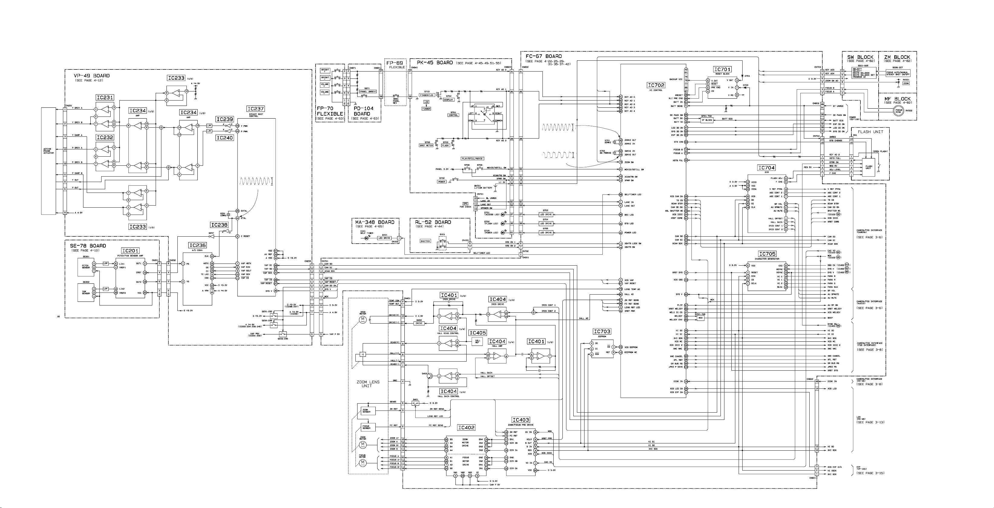
FC-67 (CAMERA Y/C PROCESS, DRAM CONTROL, LENS MOTOR DRIVE, D/A CONVERTER, AUDIO A/D.D/A CONVERTER, FD/SYSTEM CONTROL, HI CONTROL)
PRINTED WIRING BOARD
— Ref. No. FC-67 Board; 10,000 Series —
4-17
CAMERA PROCESS, AUDIO PROCESS, MOTOR DRIVE, MODE CONTROL
FC-67
4-18

FC-67 BOARD (SIDE B)
DD-119 (110)
(DC/DC CONVERTER)
PD-104
(BACK LIGHT DRIVE)
PK-45
REC PB AMP,
MOTOR DRIVE,
LCD DRIVE,
TIMING GENERATOR,
MODE SWITCH
FC-67
CAMERA Y/C PROCESS,
DRAM CONTROL, LENS
MOTOR DRIVE, D/A
CONVERTER, AUDIO
A/D.D/A CONVERTER,
FD/SYSTEM CONTROL,
HI CONTROL
C012 G-13
C013 G-13
C014 G-13
C015 G-13
C016 G-13
C017 G-13
C019 G-12
C020 G-12
C021 G-13
C022 G-12
C023 G-12
C024 F-12
C025 G-12
C026 G-12
C027 F-12
C033 G-12
C034 G-12
C035 G-13
C102 G-11
C103 F-10
C104 E-10
C107 E-10
C108 F-11
C109 F-11
C110 G-10
C113 F-10
C114 F-10
C128 G-12
C129 G-11
C130 F-10
C133 E-10
C134 E-10
C137 G-12
C138 G-10
C139 G-10
C402 G-9
C403 G-10
C404 G-10
C406 G-10
C408 G-10
C410 G-10
C413 G-10
C414 G-11
C415 G-11
C416 G-11
C418 G-11
C419 G-10
C420 G-10
C421 G-11
C451 C-11
C452 C-10
C453 F-12
C454 D-12
C455 C-10
C456 E-11
C457 E-13
C458 D-13
C459 F-11
C481 B-11
C482 B-11
C483 B-11
C484 A-11
C485 C-10
C486 E-9
C487 E-10
C488 C-11
C601 B-9
C602 B-9
C603 A-9
C604 A-9
C605 A-10
C606 A-9
C607 A-10
C608 A-10
C609 A-10
C610 A-9
C611 A-9
C612 A-9
C720 C-9
C721 B-10
C804 B-13
C805 D-13
C806 B-13
C807 D-13
C808 D-13
C809 D-13
C810 D-12
C811 B-13
C812 A-13
C813 A-13
C814 A-12
C815 E-13
FB101 F-11
FB103 F-11
FB451 D-11
FB452 D-13
FB453 E-13
FB454 F-12
FB455 F-11
FB456 E-11
FB457 D-12
FB481 B-11
FB482 E-9
FB483 C-10
FB484 E-10
FB485 C-10
FB486 B-10
FB487 B-11
FB488 C-11
FB489 C-10
FB490 D-12
FB491 D-12
FB802 E-13
IC002 G-12
IC003 G-13
IC004 G-13
IC102 F-10
IC104 G-12
IC401 G-10
IC404 G-10
IC405 G-11
IC451 D-10
IC452 D-11
IC453 E-12
IC481 B-11
IC601 B-9
IC705 B-9
IC801 C-12
IC802 A-12
IC803 A-13
IC804 D-13
IC805 A-12
IC852 D-1
L003 F-12
L005 G-13
L007 F-12
L101 G-12
L103 G-12
L104 G-12
L105 G-11
L403 G-11
L451 D-11
L452 A-11
L601 B-9
L602 A-10
L603 A-10
L604 A-9
L801 D-13
Q101 G-11
Q102 G-11
Q103 G-11
Q104 G-11
Q402 G-9
Q403 G-10
Q601 A-10
Q602 A-10
Q603 A-9
Q801 A-13
Q802 D-11
Q803 D-11
R017 G-12
R020 G-13
R021 G-13
R022 G-13
R023 G-13
R024 G-13
R025 F-13
R035 G-12
R036 G-12
R037 G-12
R039 F-12
R040 G-13
R102 F-11
R103 E-10
R104 G-10
R106 F-11
R112 G-11
R113 G-11
R115 E-10
R116 E-10
R117 G-11
R118 G-11
R120 G-11
R121 F-11
R127 G-11
R128 G-11
R132 F-11
R133 F-11
R134 F-11
R138 G-11
R139 G-12
R140 G-10
R141 G-11
R402 G-9
R406 G-9
R407 G-10
R408 G-9
R409 G-10
R410 G-10
R411 G-10
R412 G-10
R413 G-10
R414 G-10
R415 G-10
R416 G-11
R417 G-11
R418 G-11
R419 G-10
R420 G-11
R421 G-11
R422 G-11
R423 G-11
R424 G-11
R425 G-11
R426 G-11
R428 G-11
R429 G-11
R431 G-10
R451 E-11
R452 F-12
R453 F-12
R454 F-12
R455 F-11
R456 E-13
R457 C-11
R601 A-9
R605 A-10
R606 A-9
R610 A-10
R611 A-10
R612 A-10
R613 A-10
R614 A-10
R615 A-9
R616 A-9
R617 A-9
R618 A-9
R619 A-9
R620 A-9
R621 A-9
R622 A-9
R623 A-9
R624 A-9
R629 B-10
R630 A-10
R757 C-9
R802 B-12
R803 B-12
R804 B-12
R805 B-12
R806 B-12
R807 B-12
R808 C-12
R809 B-13
R810 B-13
R811 A-12
R812 D-13
R813 D-13
R814 D-13
R815 D-13
R816 C-12
R817 C-12
R818 C-12
R819 C-12
R820 C-12
R821 C-12
R822 C-12
R823 C-12
R825 A-13
R826 A-13
R827 A-13
R830 A-12
R831 A-12
R832 A-12
R870 B-12
R887 D-11
SE801 A-12
X101 F-10
X451 F-11
X803 B-12
MVC-FD91
For printed wiring boards
• This board is six-layer print board. However, the patterns of layers two to five have not been included in
the diagram.
• Chip parts
Transistor
C
BE
There are few cases that the part printed on this
diagram isn’t mounted in this model.
MVC-FD91
4-19
4-20
CAMERA PROCESS, AUDIO PROCESS, MOT OR DRIVE, MODE CONTROL
FC-67

MVC-FD91
For schematic diagram
• Refer to page 4-17 for printed wiring board.
FC-67
1
CAMERA REC/PB
60nsec
2
CAMERA REC/PB
3
4
CAMERA REC/PB
BOARD
IC101 2 – !¡
IC101 !§
60nsec
IC101 @§ CAMERA REC
78µsec
IC102 4
(1/7)
3.1Vp-p
4.0Vp-p
1.4Vp-p
9
IC102 !™,!£
CAMERA REC
60nsec
!º
IC103 #§,$∞
CAMERA REC/PB
60nsec
3Vp-p
3.8Vp-p
30nsec
5
IC102 @∞
CAMERA REC/PB
60nsec
6
IC102 $º,$¡
CAMERA REC
78µsec
7
IC102 $™,$¢
CAMERA REC
78µsec
8
IC102 9
CAMERA REC
3.8Vp-p
4.0Vp-p
8Vp-p
7.5Vp-p
60nsec
CAMERA Y/C PROCESS
FC-67 (1/7)
4Vp-p
4-22 4-23 4-24

For schematic diagram
• Refer to page 4-17 for printed wiring board.
MVC-FD91
4-25 4-26 4-27
DRAM CONTROL
FC-67 (2/7)

MVC-FD91
MVC-FD91
For schematic diagram
• Refer to page 4-17 for printed wiring board.
LENS MOTOR DRIVE
FC-67 (3/7)
4-29 4-30

For schematic diagram
• Refer to page 4-17 for printed wiring board.
MVC-FD91
FC-67
CAMERA REC/PB
!¡
60nsec
!™
!£
!¢
BOARD
IC601 5
IC601 !¢
78µsec
IC601 !ª
78µsec
IC601 @£
(4/7)
3.8Vp-p
0.1Vp-p
0.16Vp-p
!ª
@º
Q602 E
78µsec
Q603 E
78µsec
0.16Vp-p
0.1Vp-p
!∞
60nsec
!§
!¶
!•
78nsec
IC601 #¶
IC601 $§
IC601 $¶
Q601 E
0.18Vp-p
3.8Vp-p
3.3Vp-p
20msec
3.3Vp-p
78µsec
4-31 4-32 4-33
78nsec
0.18Vp-p
D/A CONVERTER
FC-67 (4/7)

MVC-FD91
MVC-FD91
For schematic diagram
• Refer to page 4-17 for printed wiring board.
AUDIO A/D.D/A CONVERTER
FC-67 (5/7)
4-35 4-36
For schematic diagram
• Refer to page 4-17 for printed wiring board.
MVC-FD91
MVC-FD91
FC-67
CAMERA REC/PB
@¡
@™
BOARD
IC801 *£
16.26MHz
IC851 *º
7.41MHz
(6/7)
5.0Vp-p
2.0Vp-p
4-37 4-38 4-39 4-40
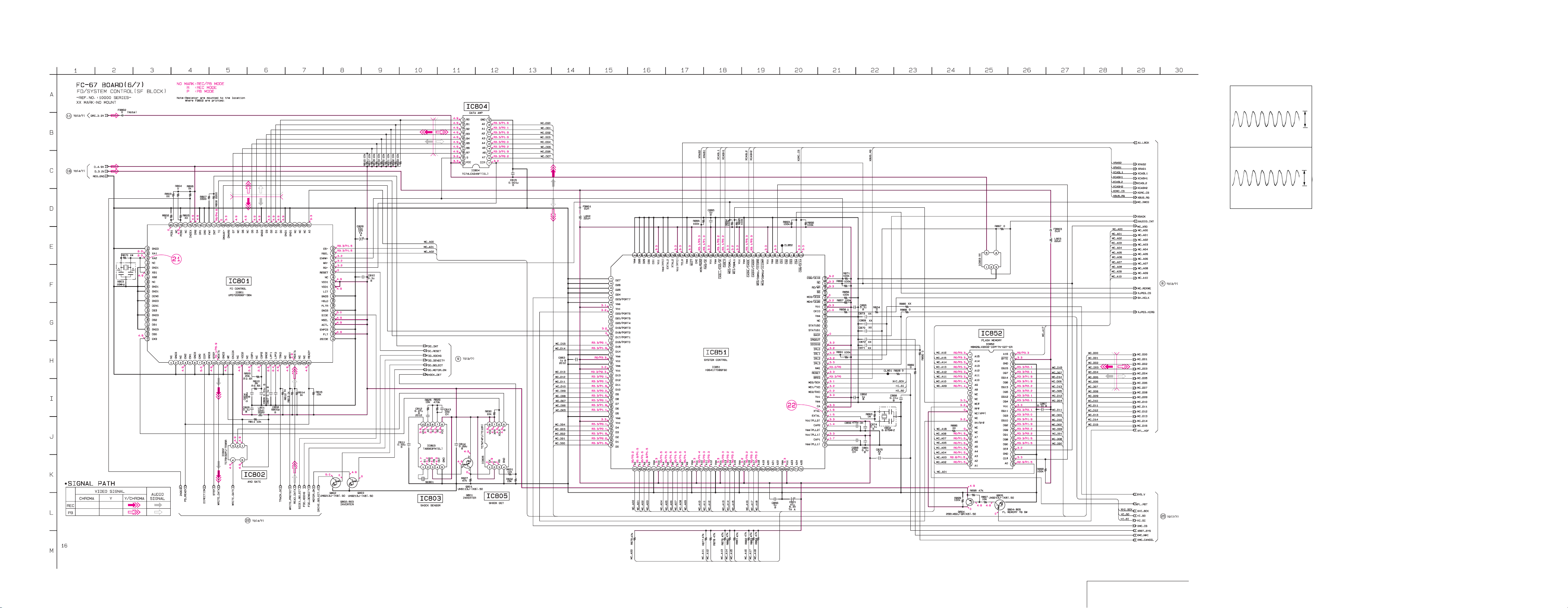
FC-67 (6/7)
FD/SYSTEM CONTROL

MVC-FD91
RL-52 BOARD
CN103 A-2
D103 A-1
D104 A-1
R121 A-1
R122 A-2
R123 A-2
R124 A-2
S101 A-2
RL-52 (RELEASE SWITCH) PRINTED WIRING BOARD
— Ref. No. RL-52 Board; 2,000 Series —
FC-67
BOARD
CAMERA REC/PB
@£
IC702 $º
20MHz
@¢
IC702 %£
32.768kHz
For schematic diagram
• Refer to page 4-17 for printed wiring board.
(7/7)
3.8Vp-p
3.4Vp-p
For printed wiring boards
• This board is six-layer print board. However, the patterns of layers two to six have not been included in the
diagram.
• Chip parts
Diode
3
21
There are few cases that the part printed on this
diagram isn’t mounted in this model.
VF-131
LCD DRIVE,
TIMING GENERATOR,
BACK LIGHT DRIVE
FLASH UNIT
MA-348
(MIC AMP, ALC)
CD-207
(CCD IMAGER)
SE-78
YAW,
PITCH SENSOR
VP-49
RL-52
(RELEASE SWITCH)
CS UNIT (Included VAP UNIT)
(STEADY SHOT DRIVE)
STEADY SHOT
CONTROL,
ACTIVE PRISM
ACTUATOR DRIVE
HI CONTROL, RELEASE SWITCH
FC-67 (7/7), RL-52
4-41 4-42 4-43 4-44

For schematic diagram
• Refer to page 4-57 for printed wiring board.
MVC-FD91
PK-45
1
CAMERA REC/PB
BOARD
IC601 $™
4.0MHz
(1/4)
3.2Vp-p
4-45 4-46 4-47
REC/PB AMP, MOTOR DRIVE
PK-45 (1/4)

MVC-FD91
MVC-FD91
For schematic diagram
• Refer to page 4-57 for printed wiring board.
PK-45
CAMERA REC/PB
2
3
4
5
BOARD
IC802 8
78µsec
IC802 9
78µsec
IC802 !º
78µsec
IC802 @º
(2/4)
0.3Vp-p
0.45Vp-p
0.25Vp-p
6
7
8
156µsec
IC802 @™
156µsec
IC802 @¢
156µsec
IC802 @•,@ª
1.5msec
4Vp-p
4Vp-p
4Vp-p
3.2Vp-p
LCD DRIVE
PK-45 (2/4)
4-49 4-50

For schematic diagram
• Refer to page 4-57 for printed wiring board.
MVC-FD91
PK-45
CAMERA REC/PB
9
!º
!¡
!™
BOARD
IC841 1
78µsec
IC841 4
20msec
IC842 @§
150nsec
IC842 #¶
(3/4)
3.3Vp-p
3.3Vp-p
4.5Vp-p
!£
IC843 7
78µsec
156µsec
3.3Vp-p
4.5Vp-p
4-534-51 4-52
PK-45 (3/4)
TIMING GENERATOR

MVC-FD91
MVC-FD91
For schematic diagram
• Refer to page 4-57 for printed wiring board.
MODE SWITCH
PK-45 (4/4)
4-55 4-56

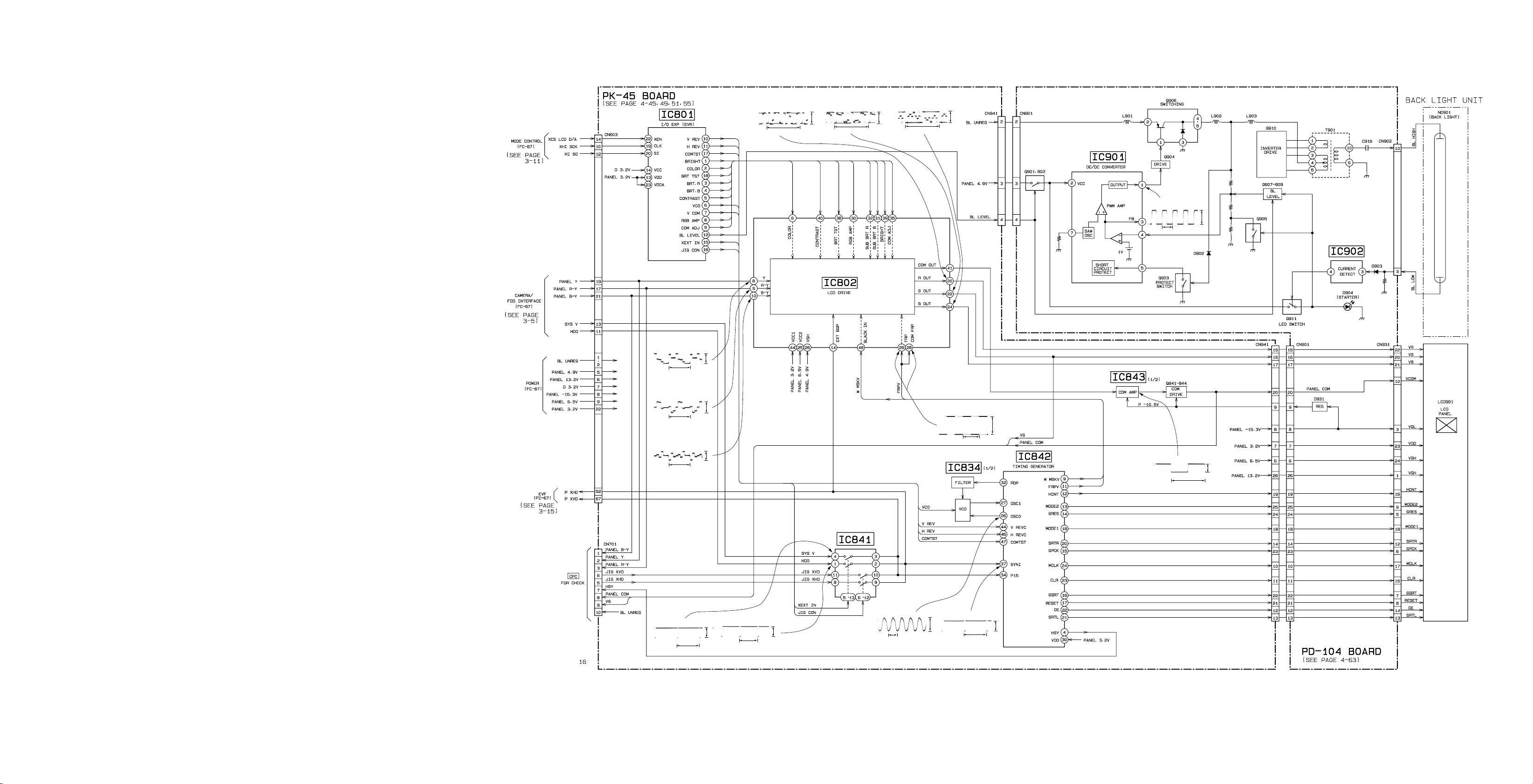
PK-45 (REC/PB AMP, MOTOR DRIVE, LCD DRIVE, TIMING GENERATOR, MODE SWITCH) PRINTED WIRING BOARD
— Ref. No. PK-45 Board; 2,000 Series —
PK-45 BOARD
BH701 D-9
C601 E-12
C602 D-12
C603 D-12
C604 C-11
C605 E-12
C606 E-12
C704 E-13
C705 E-13
C801 C-20
C802 C-20
C803 C-20
C804 A-2
C805 A-2
C806 A-19
C807 C-19
C808 C-19
C810 B-1
C811 C-19
C812 C-19
C813 C-19
C814 B-19
C815 B-19
C816 B-19
C819 B-1
C841 E-14
C842 E-14
C843 E-15
C844 E-16
C845 E-14
C846 F-17
C847 E-15
C848 F-16
C849 F-17
C850 E-14
C851 F-16
C852 E-14
C854 E-4
C857 D-14
CN601 E-11
CN602 F-12
CN603 E-6
CN701 D-10
CN702 D-19
CN941 D-16
D601 C-9
D701 D-4
D702 E-2
D703 B-9
D704 F-5
D705 D-3
D706 D-3
D707 C-1
D709 E-13
D710 E-13
D711 F-5
D712 B-9
D713 D-2
D714 F-13
D715 A-2
D841 E-16
D842 E-15
IC601 C-11
IC801 B-1
IC802 B-19
IC841 F-4
IC842 E-16
IC843 D-14
L601 E-12
L602 E-12
L801 C-19
L802 C-19
L841 E-6
L842 E-6
L843 E-15
L844 E-14
L845 F-16
Q841 D-14
Q842 D-13
Q843 D-13
Q844 E-13
R601 E-12
R602 D-11
R603 D-11
R604 E-12
R605 E-12
R606 D-11
R607 D-11
R608 D-11
R609 D-11
R610 D-11
R612 D-12
R613 D-12
R614 D-11
R615 D-11
R616 D-11
R617 D-11
R618 D-11
R619 D-11
R620 C-9
R621 D-12
R622 D-12
R623 C-11
R624 D-11
R625 C-9
R626 C-9
R627 C-9
R628 C-9
R629 E-12
R630 E-12
R631 C-12
R632 D-12
R633 D-11
R634 C-12
R635 F-12
R701 D-5
R702 D-4
R703 E-14
R704 B-9
R705 E-5
R707 E-5
R708 C-10
R708 E-2
R709 A-1
R710 D-5
R711 C-9
R712 D-4
R713 C-9
R714 E-13
R801 A-19
R802 A-19
R803 A-19
R804 A-20
R805 B-20
R806 A-19
R807 A-19
R808 A-20
R809 A-20
R810 A-19
R811 A-19
R812 A-19
R813 B-20
R814 A-20
R815 A-19
R816 A-19
R817 B-1
R818 B-1
R819 B-19
R820 B-19
R821 B-19
R822 B-19
R841 F-5
R842 D-20
R843 E-15
R844 E-15
R845 F-15
R846 F-15
R847 E-15
MVC-FD91
R848 E-16
R849 E-16
R850 E-15
R851 E-16
R852 E-15
R853 E-14
R854 E-6
R855 E-6
R856 E-15
R857 E-14
R858 F-17
R859 F-16
R861 E-14
R862 E-14
R863 E-14
R864 E-5
R865 E-14
R866 E-5
R866 E-14
R867 F-15
R869 E-14
R870 E-14
R871 E-4
R872 D-14
R873 D-14
R874 E-17
R875 D-13
R876 D-13
R877 D-13
R878 D-13
R879 E-4
R880 E-17
R881 D-14
R882 D-14
R883 E-5
R884 E-4
R885 E-15
R886 E-15
R887 E-15
R888 E-16
R889 E-16
R890 E-16
R891 E-16
S701 E-5
S702 C-1
S703 D-2
S704 D-3
S705 C-10
S708 E-7
S709 E-6
S710 B-9
X601 B-11
For printed wiring boards
• This board is six-layer print board. However, the patterns of layers two to five have not been included in
the diagram.
• Chip parts
Transistor
C
BE
There are few cases that the part printed on this
diagram isn’t mounted in this model.
4-57 4-58 4-59 4-60
PD-104
(BACK LIGHT DRIVE)
PK-45
REC PB AMP,
MOTOR DRIVE,
LCD DRIVE,
TIMING GENERATOR,
MODE SWITCH
FC-67
CAMERA Y/C PROCESS,
DRAM CONTROL, LENS
MOTOR DRIVE, D/A
CONVERTER, AUDIO
A/D.D/A CONVERTER,
FD/SYSTEM CONTROL,
HI CONTROL
DD-119 (110)
(DC/DC CONVERTER)
REC/PB AMP, LCD DRIVE, TIMING GENERAT OR
PK-45

MVC-FD91
PD-104 BOARD
C901 C-3
C901 E-3
C902 E-3
C903 D-3
C904 C-3
C905 C-3
C906 C-2
C907 C-3
C908 C-3
C909 C-2
C910 C-3
C912 D-3
C913 C-4
C914 E-3
C915 C-5
C916 E-5
C932 C-2
C933 B-1
C934 C-2
C935 B-1
C936 C-2
C991 F-1
CN901 F-3
CN902 D-4
CN931 D-1
CN971 E-1
D901 A-4
D902 D-3
D903 C-5
D904 C-5
D931 B-1
IC901 C-3
IC902 C-4
L901 E-2
L902 E-2
L903 E-3
Q901 C-4
Q902 C-4
Q903 C-4
Q904 B-2
Q905 C-4
Q906 E-2
Q907 C-4
Q908 C-4
Q909 C-4
Q910 E-3
Q911 C-5
R901 A-4
R903 C-3
R904 C-3
R905 B-3
R906 B-2
R907 B-2
R908 C-2
R909 C-4
R910 C-4
R911 C-4
R912 B-4
R913 C-4
R914 C-4
R915 B-4
R916 C-4
R917 E-3
R918 E-3
R919 C-4
R920 C-4
R921 C-5
R922 C-5
R923 C-5
R931 C-2
R932 C-2
R933 A-1
R934 B-1
R935 F-1
R936 B-1
R937 B-1
R938 B-1
R939 B-1
R940 F-1
R941 C-2
R942 C-1
R943 C-1
R944 C-1
R945 C-1
R946 C-2
R947 C-1
R948 C-1
R949 B-1
R950 C-1
R951 B-1
R952 B-1
R953 F-1
R954 B-1
R955 B-1
R956 C-1
R957 C-1
R958 C-1
R959 C-1
R960 C-1
R961 C-1
R962 C-1
R963 C-2
R971 E-1
R972 F-1
R973 E-1
R974 E-1
R975 A-2
S971 A-2
T901 F-4
MVC-FD91
PD-104 (BACK LIGHT DRIVE) PRINTED WIRING BOARD
— Ref. No. PD-104 Board; 2,000 Series —
For printed wiring boards
• This board is six-layer print board. However, the patterns of layers two to five have not been included in
the diagram.
• Chip parts
Transistor
C
BE
There are few cases that the part printed on this
diagram isn’t mounted in this model.
PD-104
(BACK LIGHT DRIVE)
PK-45
REC PB AMP,
MOTOR DRIVE,
LCD DRIVE,
TIMING GENERATOR,
MODE SWITCH
FC-67
CAMERA Y/C PROCESS,
DRAM CONTROL, LENS
MOTOR DRIVE, D/A
CONVERTER, AUDIO
A/D.D/A CONVERTER,
FD/SYSTEM CONTROL,
HI CONTROL
DD-119 (110)
(DC/DC CONVERTER)
PD-104
1
BOARD
IC901 1
CAMERA REC/PB
2µsec
5Vp-p
4-61 4-62 4-63 4-64
PD-104
BACK LIGHT DRIVE

MVC-FD91
MA-348 (MIC AMP, ALC) PRINTED WIRING BOARD
— Ref. No. MA-348 Board; 1,000 Series —
MA-348 BOARD
C101 C-1
C102 C-1
C103 C-1
C104 C-2
C105 A-2
C106 A-2
C107 C-2
C108 A-2
C109 C-2
C111 B-1
C112 B-1
C113 A-1
C114 A-1
C115 A-1
CN101 A-1
CN102 B-1
D101 C-2
D102 C-1
IC101 C-1
IC102 C-1
L101 B-1
Q101 C-2
R101 C-1
R102 C-1
R103 A-2
R105 C-1
R106 A-2
R107 A-2
R108 C-2
R109 A-2
R110 C-2
R111 A-1
R112 A-1
R113 A-1
R114 A-1
R115 A-2
R116 A-2
R117 A-2
R118 C-1
R119 C-1
R120 A-2
MVC-FD91
For printed wiring boards
• This board is six-layer print board. However, the patterns of layers two to five have not been included in
the diagram.
• Chip parts
Transistor
C
BE
There are few cases that the part printed on this
diagram isn’t mounted in this model.
VF-131
LCD DRIVE,
TIMING GENERATOR,
BACK LIGHT DRIVE
FLASH UNIT
MA-348
(MIC AMP, ALC)
CD-207
(CCD IMAGER)
SE-78
YAW,
PITCH SENSOR
VP-49
RL-52
(RELEASE SWITCH)
CS UNIT (Included VAP UNIT)
(STEADY SHOT DRIVE)
STEADY SHOT
CONTROL,
ACTIVE PRISM
ACTUATOR DRIVE
MIC AMP, ALC
MA-348
4-674-65 4-66

MVC-FD91
VF-131 BOARD
C5001 G-4
C5002 G-4
C5003 H-4
C5004 G-3
C5005 G-3
C5006 G-3
C5007 G-8
C5008 G-3
C5009 G-3
C5010 G-8
C5011 F-3
C5012 G-3
C5013 G-3
C5015 G-8
C5016 G-8
C5101 E-8
C5102 E-8
C5103 E-8
C5104 E-8
C5105 D-8
C5106 E-8
C5107 E-8
C5108 E-8
C5109 D-8
C5110 E-8
C5111 D-8
C5112 D-8
C5113 E-8
C5114 E-8
C5115 F-7
C5116 F-3
C5117 F-4
C5118 F-4
C5119 F-4
C5120 F-8
C5121 G-8
C5122 F-4
C5123 G-8
C5201 D-3
C5202 E-3
C5203 D-3
C5204 E-3
C5205 E-3
C5206 E-3
C5207 D-3
C5208 D-3
C5209 D-8
CN5001 F-4
CN5202 G-11
D5101 D-8
D5102 F-4
D5201 D-8
D5202 A-3
IC5001 G-4
IC5002 G-8
IC5101 E-8
IC5102 F-8
IC5103 F-3
L5001 G-4
L5002 G-8
L5101 D-8
L5102 F-8
L5103 F-8
L5201 E-3
L5202 D-3
ND5201 A-4
Q5046 G-8
Q5101 E-8
Q5102 E-8
Q5103 E-8
Q5104 E-8
Q5201 D-3
R5005 G-7
R5008 G-7
R5009 G-7
R5017 G-7
R5020 G-4
R5021 G-4
R5022 H-4
R5024 G-7
R5025 G-7
R5026 G-7
R5030 G-3
R5031 G-3
R5033 F-3
R5033 G-3
R5034 F-3
R5040 G-3
R5041 G-3
R5044 G-3
R5046 G-9
R5048 G-4
R5049 G-4
R5050 G-8
R5051 G-3
R5052 G-3
R5102 D-8
R5103 E-8
R5104 E-8
R5105 D-8
R5106 D-8
R5107 D-8
R5108 E-8
R5109 D-8
R5110 D-8
R5111 E-8
R5113 D-8
R5114 E-8
R5115 E-8
R5116 D-8
R5117 D-8
R5118 E-8
R5119 F-3
R5120 F-3
R5121 F-3
R5123 F-7
R5122 E-3
R5124 E-3
R5125 F-4
R5126 E-3
R5128 F-4
R5132 E-9
R5201 D-3
R5202 D-8
R5204 F-3
R5205 F-3
R5206 F-3
R5207 F-3
R5208 F-8
T5201 A-5
MVC-FD91
VF-131 (LCD DRIVE, TIMING GENERATOR) PRINTED WIRING BOARD
— Ref. No. VF-131 Board; 10,000 Series —
For printed wiring boards
• This board is six-layer print board. However, the patterns of layers two to five have not been included in
the diagram.
• Chip parts
Transistor
C
BE
There are few cases that the part printed on this
diagram isn’t mounted in this model.
VF-131
LCD DRIVE,
TIMING GENERATOR,
BACK LIGHT DRIVE
FLASH UNIT
MA-348
(MIC AMP, ALC)
CD-207
(CCD IMAGER)
SE-78
YAW,
PITCH SENSOR
VP-49
RL-52
(RELEASE SWITCH)
CS UNIT (Included VAP UNIT)
(STEADY SHOT DRIVE)
STEADY SHOT
CONTROL,
ACTIVE PRISM
ACTUATOR DRIVE
4-68 4-69 4-70
VF-131
LCD DRIVE, TIMING GENERATOR

MVC-FD91
VF-131
CAMERA REC/PB
1
2
3
4
BOARD
IC5001 8
H
IC5001 9
H
IC5001 !º
H
IC5001 @º
(1/2)
0.35Vp-p
0.35Vp-p
0.2Vp-p
VF-131
CAMERA REC/PB
7
8
9
!º
BOARD
IC5101 !∞
78µsec
IC5102 @¶
H
IC5102 #∞
H
IC5102 $¡
(2/2)
14.0Vp-p
3.2Vp-p
3.2Vp-p
5
IC5001 @™
6
IC5001 @¢
7.6Vp-p
2H
!¡
7.6Vp-p
2H
7.6Vp-p
2H
16.4MHz
IC5102 $∞
V
2.5Vp-p
3.2Vp-p
4-71 4-72 4-73 4-74
LCD DRIVE, TIMING GENERATOR
VF-131 (1/2), VF-131 (2/2)

MVC-FD91
DD-119
CAMERA REC/PB
1
2.2µsec
2
BOARD
IC301 $¢
IC301 $§
2.1µsec
0.8Vp-p
2.0Vp-p
DC/DC CONVERTER
DD-119
4-75 4-76 4-77 4-78

DD-119 (DC/DC CONVERTER) PRINTED WIRING BOARD
DD-119 (110)
(DC/DC CONVERTER)
PD-104
(BACK LIGHT DRIVE)
PK-45
REC PB AMP,
MOTOR DRIVE,
LCD DRIVE,
TIMING GENERATOR,
MODE SWITCH
FC-67
CAMERA Y/C PROCESS,
DRAM CONTROL, LENS
MOTOR DRIVE, D/A
CONVERTER, AUDIO
A/D.D/A CONVERTER,
FD/SYSTEM CONTROL,
HI CONTROL
— Ref. No. DD-119 Board; 2,000 Series —
DD-119 BOARD
C302 E-1
C303 E-1
C304 D-1
C305 D-1
C306 D-1
C307 D-1
C308 E-1
C309 D-1
C310 E-1
C311 D-2
C312 E-1
C313 D-1
C314 E-1
C315 D-1
C316 E-2
C318 E-2
C319 D-2
C320 B-2
C321 B-2
C322 E-2
C323 D-2
C324 B-2
C325 E-2
C326 E-2
C327 E-2
C328 D-2
C329 E-2
C330 E-2
C331 E-3
C332 E-3
C333 D-3
C334 A-5
C335 D-5
C336 A-4
C337 B-4
C338 D-4
C339 D-3
C340 D-4
C342 B-4
C343 E-5
C344 B-5
C345 B-4
C346 B-5
C347 B-5
C348 A-5
C349 B-5
C350 D-5
C352 D-5
C353 E-5
C354 B-6
C357 A-4
C358 A-4
C359 A-4
C360 B-6
C361 A-5
C363 B-2
C364 C-5
C365 B-6
C390 B-6
C393 B-6
CN301 A-1
CN302 E-6
CN303 E-4
D304 B-4
D305 B-4
D306 B-4
D307 B-5
D308 E-2
F301 B-2
F302 B-2
F303 B-2
F304 C-2
IC301 E-1
L301 B-3
L302 B-3
L303 A-3
L304 B-3
L305 B-3
L306 A-5
L307 D-4
L308 A-4
L309 D-3
L310 E-4
L311 D-4
L312 E-4
L313 A-5
L314 A-4
L315 A-4
L316 A-3
L317 A-4
LF301 B-2
Q306 E-3
Q307 E-4
Q308 E-3
Q309 D-3
Q310 B-4
Q311 B-5
Q312 A-5
Q313 B-5
Q314 B-5
Q315 B-5
Q316 B-5
Q317 B-5
Q318 C-6
Q319 C-5
Q320 B-5
Q321 B-5
Q322 C-6
Q323 C-5
Q324 B-5
Q325 B-5
Q326 B-5
Q327 B-5
Q328 C-5
Q329 C-5
Q330 C-5
Q331 B-5
Q332 B-5
Q333 B-6
Q334 B-6
Q335 B-6
Q336 A-5
Q337 B-6
R308 B-5
R309 E-1
R310 D-1
R312 D-1
R314 E-1
R315 E-1
R316 E-1
R317 E-1
R318 E-1
R319 E-1
R320 E-1
R321 D-1
R324 D-1
R325 D-1
R326 D-1
R327 E-1
R328 E-1
R330 E-2
R331 E-1
R332 E-1
R333 E-1
R334 E-2
R335 E-2
R336 E-1
R337 D-1
R340 D-1
R341 D-1
R342 D-1
R343 E-2
R344 A-5
R346 E-2
R347 E-2
R348 E-2
R349 D-2
R352 A-4
R353 A-4
R356 B-4
R357 B-4
R358 B-4
R360 B-5
R361 B-5
R362 B-5
R363 B-5
R364 B-5
R365 B-5
R366 B-5
R367 B-5
R368 C-6
R369 C-5
R370 A-5
R371 B-5
R372 B-6
R373 C-5
R374 B-5
R375 B-5
R376 C-5
R377 C-5
R378 C-5
R379 C-5
R380 C-5
R381 C-5
R387 B-6
R388 B-6
R389 B-6
R391 B-6
R392 B-6
R394 A-6
T301 B-4
MVC-FD91
For printed wiring boards
• This board is six-layer print board. However, the patterns of layers two to five have not been included in
the diagram.
• Chip parts
Transistor
C
BE
There are few cases that the part printed on this
diagram isn’t mounted in this model.
4-79 4-80
DC/DC CONVERTER
DD-119

MVC-FD91
MVC-FD91
MF/ZM/SW BLOCK
4-82E

SECTION 5
ADJUSTMENTS
5-1. CAMERA SECTION ADJUSTMENT
1-1. PREPARATIONS BEFORE ADJUSTMENT (CAMERA SECTION)
1-1-1. List of Service T ools
• Oscilloscope • Regulated power supply • Digital voltmeter
• Frequency counter • AC power adapter
Ref. No.
J-1
Filter for color temperature correction (C14)
ND filter 1.0
J-2
ND filter 0.3
J-3
Pattern box PTB-450
J-4
Color chart for pattern box
J-5
Siemens star chart
Adjustment remote commander (RM-95 upgraded).
J-6
(Note 2)
J-7
Clear chart for pattern box
J-8
CPC-12 jig (22P, 0.5mm)
J-9
Extension cable (10P, 0.8mm and 18P, 0.5mm)
J-10
Extension cable (50P, 0.5mm)
Alignment disk TFD2-1(+)
J-11
(Two disks as pair) TFD2-2(–)
Cleaning disk (OR-D29WA)
J-12
Cleaning disk
J-13
Personal computer with Windows95/98 installed
J-14
Power cord
J-15
Extension cable (16P, 0.5mm)
Note 1: Usage and operating note
One or two seconds of momentary use of cleaning disk is sufficient
such that FD is accessed momentarily by system control when
main power is turn on. After cleaning, insert a FD for playback.
When cleaning is insufficient, use a cleaning disk again.
Caution: Avoid using a cleaning disk excessively. Head can be
broken.
J-1 J-2
Name
J-3
Parts Code
J-6080-058-A
J-6080-808-A
J-6080-818-A
J-6082-200-A
J-6020-250-A
J-6080-875-A
J-6082-053-B
J-6080-621-A
J-6082-436-A
J-6082-427-A
J-6082-434-A
8-967-990-01
8-967-990-11
8-960-009-39
Av aila ble on market
J-6082-223-A
J-6082-357-A
Note 2: If the micro processor IC in the adjustment remote commander is
Auto white balance adjustment/check
White balance adjustment/check
White balance check
White balance check
For checking the flange back
For connecting the adjustment remote commander and
the measuring instruments
For extension between the FDD UNIT and PK-45 board
(CN601, 602)
For extension between the DD-119 board (CN303) and
the FC-67 board (CN603)
For FDD dynamic inspection and LCD system
adjustments
For FDD head cleaning (Note 1)
For checking the recorded picture
For the battery end adjustment
For extension between the CD-207 board (CN401) and
the FC-67 board (CN101)
not the new micro processor (UPD7503G-C56-12), The pages
cannot be switched. In this case, replace with the new micro
processor (8-759-148-35).
J-4 J-5
MVC-FD91
Usage
J-6
J-11 J-12
J-7 J-8
J-9 J-10
J-13 J-14 J-15
Fig. 5-1-1.
5-1

1-1-2. Preparations
Note 1: For details of how remove the cabinet and boards, refer to “2.
DISASSEMBLY”.
Note 2: When performing only the adjustments, the lens block and boards
need not be disassembled.
1) Connect the equipment for adjustments according to Fig. 5-1-5.
2) Connect the Adjustment remote commander to PK-45 board
CN701 via CPC-12 jig (J-6082-436-A). (See Fig. 5-1-3.)
3) The shutter button (RL-52 board) is need not be connected. To
remove it, disconnect the following connectors.
FC-67 board CN702 (7P, 1.0mm)
4) The ST block (Electronic viewfinder , FLASH UNIT and MIC
UNIT) is need not be connected except during “Strobe White
Balance Adjustment” and “Strobe Light Level and White
Balance Check”. To remove, disconnect the following
connectors.
1. FC-67 board CN001 (5P, 1.0mm)
2. FC-67 board CN704 (13P, 1.0mm)
3. FC-67 board CN601 (21P, 0.5mm)
Pattern box
1.5m
Front of the protection glass
Note 3: As disconnecting the FC-67 board CN602 means disconnecting
the lithium 3V power supply (PK-45 board BH701), data such as
date, time, user-set menus will be lost. After completing
adjustments, reset these data. If the FC-67 board CN602 has been
disconnected, the self-diagnosis data will be lost. Before
disconnecting, note down the self-diagnosis data (data of page: 3,
address: 2A to 3C). (Refer to “SELF-DIAGNOSIS FUNCTION”
and “5-4.Service Mode” for the self-diagnosis data.)
Note 4: Setting the “Forced Camera Power ON” Mode
1) Select page: 0, address: 01, and set data: 01.
2) Select page: F, address: 10, set data: 01, and press the PAUSE
button of the adjustment remote commander.
The above procedure will enable the camera power to be turned
on. After completing adjustments, be sure to exit the “Forced
Camera Power ON Mode”.
Note 5: Exiting the “Forced Camera Power ON” Mode
1) Select page: 0, address: 01, and set data: 01.
2) Select page: F, address: 10, set data: 00, and press the PAUSE
button of the adjustment remote commander.
3) Select page: 0, address: 01, and set data: 00.
Fig. 5-1-2.
1-1-3. Discharging of the flashlight power supply
The capacitor which is used as power supply of flashlight is charged
with 200V to 300V voltage. Discharge this voltage before starting
adjustments in order to protect service engineers from electric shock
during adjustment.
Discharge procedure
1. Press the FLASH button (PK-45 board S703) and turn off the
FLASH LED (PK-45 board D702).
2. F abricate the dischar ging jig as shown in F ig. 5-1-4 locally by
yourself. Connect the discharging jig to the positive (+) and
negative (-) terminal of the flash voltage char ge capacitor. Allo w
ten seconds to discharge the voltage.
PK-45 board
CN701
Fig. 5-1-3.
Insulator side
CPC-12 jig
22 pin flexible
Capacitor
R : 1kΩ 1W
Parts code :
1-215-869-11
FLASH UNIT
Fig. 5-1-4.
5-2

Adjustment
remote commander
CPC-12
(J-6082-436-A)
LANC
jack
Oscilloscope
CH1
EXT.TRIG.
VG
COM
GND
8
4
9
Must be connected
when the electronic
viewfineder
is used.
Must be connected
when the FLASH UNIT
is used.
Must be connected
when the MIC UNIT is used.
PK-45
board
CN941
CN603
CN602
CN601
CN701
FDD UNIT
CN013
CN012
CN011
Extension cable
(J-6082-427-A)
Extension cable
(16P, 0.5mm)
(J-6082-357-A)
CD-207 board
Lens block
SW
BLOCK
ZM
BLOCK
CN702
CN704
CN401
CN001
CN101
CN701
CN601
CN603
FC-67
board
CN703
CN602
CN301
DD-119
board
CN303
RL-52 board
CN103
AC power adaptor
(BC-V615)
Extension cable (50P, 0.5mm)
(J-6082-434-A)
BATTERY
HOLDER
MF UNIT
CN401
Note 1: When connecting the extension cable,
refer to “1. Connection between the FDD
unit and PK-45 board” of page 6.
Note 2: In changing data, wait for more than 5 seconds
after the set was turned on, then change the data.
Note 3: Connect the GND terminal to Floppy disk drive unit
frame when check the RF signal waveform.
Fig. 5-1-5.
5-3

m
1-1-4. Precaution
1. Setting the Switch
Unless otherwise specified, set the switches as follows and perform
adjustments without loading cassette.
1. PLAY/STILL/MOVIE switch
(PK-45 board S708, 709) ............................................. STILL
2. FOCUS switch (FRONT SW block)..................... MANUAL
3. STEADY SHOT switch (FRONT SW block).................. OFF
4. PROGRAM AE switch (SIDE SW block)
........................................ Auto (No mark indicated on LCD)
5. WHITE BALANCE switch (SIDE SW block)
........................................ Auto (No mark indicated on LCD)
2. Order of Adjustments
Basically carry out adjustments in the order given.
Color bar chart standard picture frame
A=B
A
B
Cyan
Yellow
White
Green
C=D
C
Red
Magenta
D
0 ± 0.1msec
Blue
H
External trigger : CN701
Fig. a VG signal waveform (CN701 9 pin of PK-45 board)
Electron beam scan frame size
Red
White
Cyan
Green
Yellow
Fig. b (LCD screen)
Magenta
8
LCD picture frame
Blue
H
pin (COM) External trigger : CN701 !¡ pin (LANC IN)
3. Subjects
1) Color bar chart (Standard picture frame)
When performing adjustments using the color bar chart, adjust
the picture frame as shown in Fig. 5-1-6. (Standard picture
frame)
2) Clear chart (Standard picture frame)
Remove the color bar chart from the pattern box and insert a
clear chart in its place. (Do not perform zoom operations during
this time.)
3) Flange back adjustment chart
Make the chart shown in Fig. 5-1-7 using A0 size
(1189mm × 841mm) black and white vellum paper.
V
Adjust the camera zoom and direction to
obtain the output waveform shown in Fig. a
and the LCD screen shown in Fig. b.
Fig.5-1-6.
White
841m
Black
1189mm
Note: Use matte vellum paper bigger than A0, and make sure the edges of
the black and white paper joined together are not rough.
5-4
Fig. 5-1-7.

1-2. INITIALIZATION OF F, E PAGE DATA
1. Initializing the F, E Page Data
Note: If the F, E page data is initialized, all adjustments must be performed
again.
Adjusting page
Adjusting Address
Adjusting page
Adjusting Address
Initializing Method:
1) Select page: 0, address: 01, and set data: 01.
2) Select page: 3, address: 00, and set data: 2D.
3) Select page: 3, address: 01, set data: 2D, and press the PAUSE
button of the adjustment remote commander.
4) Select page: 3, address: 00, and check that the data is “00”.
5) Perform “Modification of F, E Page Data”.
2. Modification of F, E Page Data
If the F, E Page data has been initialized, change the data of the
“Fixed data-2” address shown in the following tables by manual
input.
Modifying Method:
1) Before changing the data, select page: 0, address: 01, and set
data: 01.
2) New data for changing are not shown in the tables because
they are different in destination. When chang ing the data, copy
the data built in the same model.
Note :If copy the data built in the different model, the camcorder may
not operate.
3) When changing the data, press the PAUSE button of the
adjustment remote commander each time when setting new
data to write the data in the non-volatile memory.
4) Check that the data of adjustment addresses is the initial value.
If not, change the data to the initial value.
Processing after Completing Modification of F, E Page data
1) Select page: 3, address: 00, and set data: 29.
2) Select page: 3, address: 01, and set data: 29, and press the
PAUSE button of the adjustment remote commander.
3) Perform all adjustments.
3. F Page Table
Note: Fixed data-1 : Initialized data. (Refer to “1. Initializing the F, E
Page Data”.)
Fixed data-2 : Modified data. (Refer to “2. Modification of F, E
Page Data”.)
Address
Initial value
00 to 0F
10
00
11
12
13
14
15
16
17
18
19
1A
1B
1C
80
88
AD
C2
CD
F
00 to FF
E
00 to FF
Remark
Test mode
Fixed data-1
Fixed data-2
Fixed data-1
(Initialized data)
Battery end adj.
Address
1D
1E
1F
20
21
22
23
24
25
26
27
28
29
2A
2B
2C
2D
2E
2F
30
31
32
33
34
35
36
37
38
39
3A
3B
3C
3D
3E
3F
40
41
42
43
44
45
46
47
48
49
4A
4B
4C
4D
4E
4F
50
51
52
53
54
Initial value
BB
6F
77
7A
DB
6F
97
78
7C
Remark
Fixed data-1
(Initialized data)
Fixed data-2
Fixed data-1
(Initialized data)
Fixed data-2
Fixed data-1
(Initialized data)
Fixed data-2
Fixed data-1
Bright adj. (LCD)
Color adj. (LCD)
White balance adj. (LCD)
Contrast adj. (LCD)
VCO adj. (LCD)
V-COM adj. (LCD)
D range adj. (LCD)
V-COM level adj. (LCD)
Fixed data-1
(Initialized data)
Fixed data-2
Fixed data-1
(Initialized data)
Fixed data-2
Fixed data-1
(Initialized data)
Fixed data-2
Fixed data-1
(Initialized data)
Fixed data-2
Fixed data-1
(Initialized data)
Fixed data-2
Fixed data-1
(Initialized data)
5-5

Address
55
56
57
58
59
5A
5B
5C
5D
5E
5F
60
61
62
63
64
65
66
67
68
69
6A
6B
6C
6D
6E
6F
70
71
72
73
74
75
76
77
78
79
7A
7B
7C
7D
7E
7F
80
81
82
83
84
85
86
87
88
89
8A
8B
8C
Initial value
80
80
30
B0
98
80
Remark
Fixed data-1
(Initialized data)
Fixed data-2
Fixed data-1
Fixed data-2
Fixed data-1
Fixed data-2
(Modified data, copy the data built in
the same model.)
Fixed data-1
(Initialized data)
Fixed data-2
White balance adj. (EVF)
Fixed data-1
Fixed data-2
VCO adj. (EVF)
Back light consumption current adj. (EVF)
Fixed data-1
Fixed data-2
Bright adj. (EVF)
Contrast adj. (EVF)
Fixed data-1
(Initialized data)
Fixed data-2
Fixed data-1
(Initialized data)
Fixed data-2
Fixed data-1
Fixed data-2
Fixed data-1
(Initialized data)
Address
8D
8E
8F
90
91
92
93
94
95
96
97
98
99
9A
9B
9C
9D
9E
9F
A0
A1
A2
A3
A4
A5
A6
A7
A8
A9
AA
AB
AC
AD
AE
AF
B0
B1
B2
B3
B4
B5
B6
B7
B8
B9
BA
BB
BC
BD
BE
BF
C0
C1
C2
C3
C4
Initial value
56
19
E0
21
E7
11
00
00
23
00
19
00
11
Remark
Fixed data-1
(Initialized data)
Fixed data-2
Fixed data-1
(Initialized data)
Flange back adj.
Fixed data-1
(Initialized data)
Flange back adj.
5-6

Address
C5
C6
C7
C8
C9
CA
CB
CC
CD
CE
CF
D0
D1
D2
D3
D4
D5
D6
D7
D8
D9
DA
DB
DC
DD
DE
DF
E0
E1
E2
E3
E4
E5
E6
E7
E8
E9
EA
EB
EC
ED
EE
EF
F0
F1
F2
F3
F4
F5
F6
F7
F8
F9
FA
FB
FC
Initial value
00
78
80
70
73
45
39
06
60
B2
46
Remark
Flange back adj.
Fixed data-1
HALL adj.
Fixed data-1
Light level adj.
AWB standard data input
Fixed data-1
Fixed data-2
Auto white balance adj.
Fixed data-2
Fixed data-1
(Initialized data)
Fixed data-2
Fixed data-1
(Initialized data)
Fixed data-2
(Modified data, copy the data built in
the same model.)
Fixed data-1
(Initialized data)
Fixed data-2
Fixed data-1
(Initialized data)
Fixed data-2
Fixed data-1
(Initialized data)
Fixed data-2
Fixed data-1
Address
FD
FE
Initial value
Fixed data-1
(Initialized data)
Remark
FF
Table. 5-1-1.
4. E Page table
Note: Fixed data-1 : Initialized data. (Refer to “1. Initializing the F, E
Page Data”.)
Fixed data-2 : Modified data. (Refer to “2. Modification of F, E
Page Data”.)
Address
00
01
02
Initial value
Fixed data-2
(Modified data, copy the data built in
the same model.)
Remark
03
04
05
Fixed data-1
Fixed data-2
06
07
08
09
0A
0B
0C
0D
0E
Fixed data-1
(Initialized data)
0F
10
11
12
13
14
15
16
17
18
19
1A
1B
1C
Fixed data-2
Fixed data-1
(Initialized data)
1D
1E
1F
20
21
22
23
24
25
26
27
28
29
2A
2B
2C
14
F8
ED
FF
03
F1
3B
27
08
HALL adj.
Fixed data-1
(Initialized data)
Fixed data-2
Fixed data-1
Color reproduction adj.
Fixed data-1
(Initialized data)
5-7

Address
2D
2E
2F
30
31
32
33
34
35
36
37
38
39
3A
3B
3C
3D
3E
3F
40
41
42
43
44
45
46
47
48
49
4A
4B
4C
4D
4E
4F
50
51
52
53
54
55
56
57
58
59
5A
5B
5C
5D
5E
5F
60
61
62
63
64
Initial value
27
77
Remark
Fixed data-1
(Initialized data)
Strobe white balance adj.
Fixed data-1
(Initialized data)
Fixed data-2
Fixed data-1
(Initialized data)
Fixed data-2
Fixed data-1
(Initialized data)
Address
65
66
67
68
69
6A
6B
6C
6D
6E
6F
70
71
72
73
74
75
76
77
78
79
7A
7B
7C
7D
7E
7F
80
81
82
83
84
85
86
87
88
89
8A
8B
8C
8D
8E
8F
90
91
92
93
94
95
96
97
98
99
9A
9B
9C
Initial value
00
Remark
Fixed data-1
(Initialized data)
Fixed data-2
Fixed data-1
(Initialized data)
Fixed data-2
Fixed data-1
Fixed data-2
Fixed data-1
(Initialized data)
Fixed data-2
Fixed data-1
Strobe light level adj.
Fixed data-1
(Initialized data)
Fixed data-2
Fixed data-1
(Initialized data)
Fixed data-2
Fixed data-1
5-8

Address
9D
9E
9F
A0
A1
A2
A3
A4
A5
A6
A7
A8
A9
AA
AB
AC
AD
AE
AF
B0
B1
B2
B3
B4
B5
B6
B7
B8
B9
BA
BB
BC
BD
BE
BF
C0
C1
C2
C3
C4
C5
C6
C7
C8
C9
CA
CB
CC
CD
CE
CF
D0
D1
D2
D3
D4
Initial value
62
62
00
00
00
00
00
00
00
00
00
00
00
00
00
00
00
00
00
00
00
Remark
Fixed data-1
(Initialized data)
Steady shot adj.
Fixed data-1
(Initialized data)
Fixed data-2
Fixed data-1
(Initialized data)
Fixed data-2
Fixed data-1
(Initialized data)
CCD defect compensation
Address
D5
D6
D7
D8
D9
DA
DB
DC
DD
DE
DF
E0
E1
E2
E3
E4
E5
E6
E7
E8
E9
EA
EB
EC
ED
EE
EF
F0
F1
F2
F3
F4
F5
F6
F7
F8
F9
FA
FB
FC
FD
FE
FF
Initial value
00
Remark
CCD defect compensation
Fixed data-1
(Initialized data)
Fixed data-2
Fixed data-1
Fixed data-2
Fixed data-1
(Initialized data)
Fixed data-2
Fixed data-1
(Initialized data)
Table. 5-1-2.
5-9

1-3. CAMERA SYSTEM ADJUSTMENTS
e
1. Picture Frame Setting
Subject Color bar chart standard picture frame
(1.5m from the front of the protection
glass)
Measurement Point Pin 9 of CN701 (VG) of PK-45 board
External trigger (Horizontal period) :
Pin 8 of CN701 (COM) of PK-45 board
External trigger (Vertical period) :
Pin !¡ of CN701 (LANC IN) of PK-45
board
Measuring Instrument Oscilloscope and LCD screen
Specified Value A=B, C=D, t=0 ± 0.1msec
Setting method:
1) Adjust the focus using the focus ring.
2) Adjust the zoom and the camera direction, and set to the
specified position.
3) Mark the position of the picture frame on the LCD screen, and
adjust the picture frame to this position in following adjustments
using “Color bar chart standard picture frame”.
Check on the oscilloscope
1. Horizontal period
A=B
A
B
C=D
C
H
Fig. 5-1-8.
2. Vertical period
D
H
t
Fig. 5-1-9.
Check on the LCD screen
Electronic beam scanning frame
Cyan
White
Green
Yellow
Magenta
Fig. 5-1-10.
V
Red
Blue
LCD picture fram
5-10

2. HALL Adjustment
For detecting the position of the lens iris, adjust the hall AMP gain
and offset.
Subject Not required
Adjustment Page F E
Adjustment Address C7, C8 1E
Note: Check that the data of page: 2, address: 02 is 00. If not, select page:
2, address: 01, set data: 00 and press the PAUSE button of the
adjustment remote commander.
Adjusting method:
1) Select page: 0, address: 01, and set data: 01.
2) Select page: 2, address: 01, set data: 6D, and press the PAUSE
button of the adjustment remote commander. (The HALL
adjustment is performed and the adjustment data is stored in
page: F, address: C7, C8 and page: E, address: 1E.)
3) Select page: 2, address: 02, and check that the data is “01”.
Processing after Completing Adjustments
1) Select page: 2, address: 01, set data: 00, and press the P AUSE
button of the adjustment remote commander.
2) Select page: 0, address: 01, and set data: 00.
3. Flange Back Adjustment
The inner focus lens flange back adjustment is carried out
automatically. In whiche v er case, the focus will be de viated during
auto focusing/manual focusing.
Subject Flange back adjustment chart
(2.0 m from the front of the protection
glass)
(Luminance: 350 ± 50 lux)
Measurement Point Check operation on LCD screen
Measuring Instrument
Adjustment Page F
Adjustment Address B6 to BB, BE to C5
Adjusting method:
1) Check that at both the zoom lens TELE end and WIDE end,
the center of the chart for the flange back adjustment and center
of the exposure screen coincide.
2) Select page: 0, address: 01, and set data: 01.
3) Check that the data of page: F, addr ess: B6 to BB, BE to C5 is
the initial value (See table below).
Address
B6
B7
B8
B9
BA
BB
BE
Data
56
19
E0
21
E7
11
00
Address
BF
C0
C1
C2
C3
C4
C5
Data
00
23
00
19
00
11
00
4) Select page: 2, address: 02, and check that the data is “00”.
5) Select page: 2, address: 01, set data: 13, and press the P AUSE
button of the adjustment remote commander.
6) Select page: 2, address: 01, set data: 15, and press the P AUSE
button of the adjustment remote commander.
(The adjustment data will be automatically input to page: F,
addresses: B6 to BB, BE to C5.)
7) Select page: 2, address: 02, and check that the data is “01”.
Processing after Completing Adjustments
1) Select page: 2, address: 01, set data: 00, and press the P AUSE
button of the adjustment remote commander.
2) Select page: 0, address: 01, and set data: 00.
5-11

4. Flange Back Check
Subject Siemens star
(2.0 m from the front of the protection
glass)
(Luminance : approx. 200 lux)
Measurement Point Check operation on LCD screen
Measuring Instrument
Specified Value Focused at the TELE end and WIDE
end.
Checking method:
1) Place the siemens star 2.0m from the front of the protection
glass).
2) Shoot the siemens star with the zoom TELE end.
3) Turn on the auto focus.
4) Check that the lens is focused.
5) Select page: 2, address: 21, and set data: 10.
6) While observe the LCD screen, change the zoom to the WIDE
end and check that the lens is focused.
Processing after Completing Adjustments
1) Select page: 2, address: 21, and set data: 00.
5. Light Level Adjustment
Adjust the standard LV value.
Subject Clear chart
(Color bar standard picture frame)
Adjustment Page F
Adjustment Address CA, CB
Note: Check that the data of page: 2, address: 02 is 00. If not, select page:
2, address: 01, set data: 00 and press the PAUSE button of the
adjustment remote commander.
Adjusting method:
1) Select page: 0, address: 01, and set data: 01.
2) Select page: 2, address: 10, and set data: 58.
3) Select page: 2, address: 01, set data: 0D, and press the P AUSE
button of the adjustment remote commander.
(When the adjustment data is take in, the data will be
automatically input to page: F, address: CA and CB.)
4) Select page: 2, address: 02, and check that the data is “01”.
Processing after Completing Adjustments
1) Select page: 2, address: 01, set data: 00, and press the PAUSE
button of the adjustment remote commander.
2) Select page: 2, address: 10, and set data: 00.
3) Select page: 0, address: 01, and set data: 00.
5-12

6. Auto White Balance Standard Data Input
Subject Clear chart
(Color bar standard picture frame)
Adjustment Page F
Adjustment Address CC to CF
Note: Check that the data of page: 2, address: 02 is 00. If not, select page:
2, address: 01, set data: 00 and press the PAUSE button of the
adjustment remote commander.
Adjusting method:
1) Select page: 0, address: 01, and set data: 01.
2) Select page: E, address: 11, set data: 0A, and press the PAUSE
button of the adjustment remote commander.
3) Select page: 2, address: 10, and set data: 58.
4) Select page: 2, address: 01, set data: 11, and press the P AUSE
button.
5) Select page: 2, address: 01, set data: 0B, and press the P AUSE
button.
(When the standard data is take in, the data will be automatically
input to page: F, address: CC to CF.)
6) Select page: 2, address: 02, and check that the data is “01”.
Processing after Completing Adjustments
1) Select page: 2, address: 01, and set data: 00, and press the
PAUSE button of the adjustment remote commander.
2) Select page: E, address: 11, set data: 18, and press the PAUSE
button.
3) Select page: 2, address: 10, and set data: 00.
4) Select page: 0, address: 01, and set data: 00.
7. Auto White Balance Adjustment
Adjust to the proper auto white balance output data.
If it is not correct, auto white balance and color reproducibility will
be poor.
Subject Clear chart
(Color bar standard picture frame)
Filter Filter C14 for color temperature
correction
Measurement Point DDS display of LCD screen (Note 2)
Measuring Instrument
Adjustment Page F
Adjustment Address D3, D4
Specified Value R ratio: 2B40 to 2BC0
B ratio: 5E40 to 5EC0
Note 1: Perform “Auto White Balance Standard Data Input” before this
adjustment.
Note 2: The right four digits of the display data is the object data.
00:XX:XX
Object data
Adjusting method:
1) Place the C14 filter for color temperature correction on the
lens.
2) Select page: 0, address: 01, and set data: 01.
3) Select page: E, address: 11, set data: 0A, and press the P A USE
button of the adjustment remote commander.
4) Select page: F, address: 11, set data: 02, and press the PAUSE
button.
5) Select page: 2, address: 10, and set data: 58.
6) Select page: 2, address: 01, and set data: 3F, and press the
PAUSE button.
7) Select page: 0, address: 03, and set data: 04.
8) Select page: F, address: D3, change the data and adjust the
average value of the DDS display data (Note 2) to the R ratio
specified value.
9) Press the PAUSE button.
10) Select page: 0, address: 03, and set data: 05.
11) Select page: F, address: D4, change the data and adjust the
average value of the DDS display data (Note 2) to the B ratio
specified value.
12) Press the PAUSE button.
Processing after Completing Adjustments
1) Select page: E, address: 11, set data: 18, and press the PAUSE
button of the adjustment remote commander.
2) Select page: F, address: 11, set data: 00, and press the PAUSE
button.
3) Select page: 0, address: 01, and set data: 00.
4) Select page: 0, address: 03, and set data: 00.
5) Select page: 2, address: 01, set data: 00, and press the P AUSE
button.
6) Select page: 2, address: 10, and set data: 00.
5-13

8. Color Reproduction Adjustment
Adjust the color separation matrix coefficient so that proper color
reproduction is produced.
Subject Color bar chart standard picture frame
Measurement Point CHX: Pin 1 of CN701 of PK-45
board (PANEL B-Y)
CHY: Pin 3 of CN701 of PK-45
board (PANEL R-Y)
Measuring Instrument Oscilloscope (X-Y mode)
Adjustment Page E
Adjustment Address 23, 24, 25, 26, 27, 28, 29. 2A
Specified Value All color luminance points should
settle within each color reproduction
frame.
Note 1: This adjustment should be carried out upon completion of “6. Auto
White Balance Standard Data Input”.
Switch setting:
1) FINDER/LCD ................................................................. LCD
Preparations before adjustments
1) Set to the PLAY mode.
2) Playback the color bar signal (MVC-001C.JPG) of the
alignment disk (TFD2-1(+) or TFD2-2(–)).
3) Select page: 0, address: 01, and set data: 01.
4) Select page: 3, address: 02, and set data: 01.
5) Select page: F , address: E0, set data: 40, and press the PAUSE
button of the adjustment remote commander.
6) Adjust the X POSITION and Y POSITION of the oscilloscope,
and adjust the black luminance point to the center of the CRT
screen.
7) Adjust the Xch GAIN and Yc h GAIN of the oscilloscope, and
settle each color luminance point in each color reproduction
frame (frame of the thin line).
8) Repeat steps 6) to 7) until each color luminance point settled
in each color reproduction frame (frame of the thin line).
9) Set to the camera (STILL) mode.
Adjusting method:
1) Select page: 0, address: 01, and set data: 01.
2) Select page: 2, address: 10, and set data: 59.
3) Select page: 2, address: 01, set data: 0F, and press the PAUSE
button.
4) Adjust the X POSITION and Y POSITION of the oscilloscope,
and adjust the black luminance point to the center of the CRT
screen.
5) Change the data of page: E, address: 23, 24, 27 and 28, and
settle the yellow and blue luminance points in each color
reproduction frame (frame of the thick line).
Note 2:Be sure to press the PAUSE button of the adjustment remote
commander before changing the addresses. If not, the new
data will not be written to the memory.
6) Adjust the X POSITION and Y POSITION of the oscilloscope,
and adjust the black luminance point to the center of the CRT
screen.
7) Change the data of page: E, address: 25, 26, 29 and 2A, and
settle the red, magenta,cyan and green luminance points in each
color reproduction frame (frame of the thick line).
Note 2:Be sure to press the PAUSE button of the adjustment remote
commander before changing the addresses. If not, the new
data will not be written to the memory.
8) Repeat steps 4) to 7) until all color luminance point settled
within each color reproduction frame (frame of the thick line).
Processing after Completing Adjustments
1) Select page: F , address: E0, set data: 1B, and press the PA USE
button .
2) Select page: 0, address: 01, set data: 00.
3) Select page: 2, address: 01, and set data: 00, and press the
PAUSE button .
4) Select page: 2, address: 10, set data: 00.
5) Select page: 3, address: 02, and set data: 00.
: For preparation
: For adjustment
Black luminance point
Fig. 5-1-11.
5-14

9. White Balance Check
Subject Clear chart
(Color bar standard picture frame)
Filter ND filter 1.0 and 0.3
Measurement Point Display data of page: 1
Measuring Instrument Adjustment remote commander
Specified V alue R-Y data:
FC to FF or 00 to 04 (Note1)
B-Y data:
FC to FF or 00 to 04 (Note1)
Light level data:
Without ND filter:
0E10 or more (Note2)
With ND filter 1.3:
0D00 or less (Note2)
Note 1: Displayed data of page 1 of the adjustment remote commander.
1 : XX : XX
R-Y data
B-Y data
Note 2: Displayed data of page 1 of the adjustment remote commander.
1 : XX : XX
Light level data
Checking method:
1) Check that the lens is not covered with the ND filter.
2) Select page: 0, address: 01, and set data: 01.
3) Select page: E, address: 11, set data: 15, and press the PAUSE
button of the adjustment remote commander.
4) Select page: 0, address: 03, and set data: 02.
5) Select page: 2, address: 10, and set data: 58.
6) Select page: 2, address: 56, and set data: 56.
7) Select page: 2, address: 01, set data: 0F, and press the PAUSE
button.
8) Select page: 1, and check that the R-Y data satisfies the specified
value and the B-Y data satisfies the specified value. (Note1)
9) Select page: 0, address: 03, and set data: 06.
10) Select page: 1, and check that the light level data satisfies the
specified value. (Note2)
11) Place the ND 1.3 filter on the lens.
12) Select page: 1, and check that the light level data satisfies the
specified value. (Note2)
Processing after Completing Adjustments
1) Select page: 2, address: 01, set data: 00, and press the P AUSE
button of the adjustment remote commander.
2) Select page: 2, address: 10, and set data: 00.
3) Select page: 2, address: 56, and set data: 00.
4) Select page: E, address: 11, set data: 18, and press the PAUSE
button.
5) Select page: 0, address: 01, and set data: 00.
6) Select page: 0, address: 03, and set data: 00.
10. Strobe Light Level Adjustment
Adjust the minimum gain when the strobe light flashes.
Subject Clear chart
(Color bar standard picture frame)
Measurement Point Display data of page : 1
Measuring Instrument Adjustment remote commander
Adjustment Page E
Adjustment Address 81
Specified Value 01E7 to 0267
Note: Displayed data of page 1 of the adjustment remote commander.
1 :XX:XX
Object data
Adjusting method:
1) Select page: 0, address: 01, and set data: 01.
2) Select page: E, address: 70, set data: 03, and press the PAUSE
button of the adjustment remote commander.
3) Select page: E, address: 71, set data: 00, and press the PAUSE
button.
4) Select page: 2, address: 10, and set data: 58.
5) Select page: 2, address: 01, set data: 9D, and press the P A USE
button.
6) Select page: 1, and read the display data (Note). If the display
data lies within the “0207” to “0247” range, perform
“Processing after Completing Adjustments”.
7) Select page: E, address: 81, change the data, and press the
PAUSE button.
8) Select page: 1, and check that the display data lies within the
“0207” to “0247” range. If not, repeat steps 7) to 8).
9) Select page: 2, address: 01, set data: 00, and press the P AUSE
button.
10) Select page: 2, address: 01, set data: 9D, and press the PA USE
button.
11) Select page: 1, and check that the display data satisfies the
specified value.
Processing after Completing Adjustments
1) Select page: E, address: 70, set data: 00, and press the PAUSE
button of the adjustment remote commander.
2) Select page: E, address: 71, set data: 00, and press the PAUSE
button.
3) Select page: 0, address: 01, and set data: 00.
4) Select page: 2, address: 01, set data: 00, and press the P AUSE
button of the adjustment remote commander.
5) Select page: 2, address: 10, and set data: 00.
5-15

11. Strobe White Balance Adjustment
Adjust the white balance when the strobe light flashes.
Subject A plate which reflection rate is 18%
(1.0m from the front of the protection
glass)
Measurement Point Display data of page : 1
Measuring Instrument Adjustment remote commander
Adjustment Page E
Adjustment Address 42, 43
Note 1: Perform this adjustment in the dark room or use a dark box.
Note 2: An y light other than the strobe light should not light up the plate.
Note 3: Displayed data of page 1 of the adjustment remote commander.
1 :XX:XX
Strobe B data
Strobe R data
Switch setting:
1) Flash emitter .................................................................. Open
Adjusting method:
1) Select page: 0, address: 01, and set data: 01.
2) Select page: E, address: 11, set data: 15, and press the P AUSE
button of the adjustment remote commander.
3) Select page: 2, address: 10, and set data: 58.
4) Select page: 2, address: 56, and set data: 89.
5) Select page: 2, address: 90, and set data: 00.
6) Select page: 2, address: 91, and set data: 00.
7) Select page: 2, address: 92, and set data: 00.
8) Select page: 2, address: 93, and set data: 80.
9) Select page: 2, address: 01, set data: 79, and press the PAUSE
button.
10) Select page: 2, address: 01, set data: 67, and press the PAUSE
button.
11) Check the flashing of the strobe light.
12) Select page: 0, address: 03, and set data: 05.
13) Select page: 1, and read the strobe R data and strobe B data.
14) Select page: E, address: 42, set the strobe R data, and press the
PAUSE button.
15) Select page: E, address: 43, set the strobe B data, and press the
PAUSE button.
Processing after Completing Adjustments
1) Select page: E, address: 11, set data: 18, and press the P AUSE
button of the adjustment remote commander.
2) Select page: 0, address: 01, and set data: 00.
3) Select page: 0, address: 03, and set data: 00.
4) Select page: 2, address: 01, set data: 00, and press the PAUSE
button of the adjustment remote commander.
5) Select page: 2, address: 10, and set data: 00.
6) Select page: 2, address: 56, and set data: 00.
7) Select page: 2, address: 90, and set data: 00.
8) Select page: 2, address: 91, and set data: 00.
9) Select page: 2, address: 92, and set data: 00.
10) Select page: 2, address: 93, and set data: 00.
12. Strobe Light Level and White Balance Check
Check the light level regulation and the white balance when the
strobe light flashes.
Subject A plate which reflection rate is 18%
(1.0m from the front of the protection
glass)
Measurement Point Display data of page : 1
Measuring Instrument Adjustment remote commander
Specified Value Y level data : 70 to 95 (Note 3)
R-Y data : F A t o F F o r 0 0 t o 0 6 (Note 4)
B-Y data : F A t o F F o r 0 0 t o 0 6 (Note 4)
Note 1: Perform this adjustment in the dark room or use a dark box.
Note 2: An y light other than the strobe light should not light up the plate.
Note 3: Display data of page 1 of the adjustment remote commander.
1 :00:XX
Y level data
Note 4: Display data of page 1 of the adjustment remote commander.
1 :XX:XX
B-Y data
R-Y data
Switch setting:
1) Flash emitter .................................................................. Open
Adjusting method:
1) Select page: 0, address: 01, and set data: 01.
2) Select page: E, address: 11, set data: 15, and press the P AUSE
button of the adjustment remote commander.
3) Select page: 2, address: 10, and set data: 58.
4) Select page: 2, address: 56, and set data: 89.
5) Select page: 2, address: 90, and set data: 00.
6) Select page: 2, address: 91, and set data: 00.
7) Select page: 2, address: 92, and set data: 00.
8) Select page: 2, address: 93, and set data: 80.
9) Select page: 2, address: 01, set data: 79, and press the PAUSE
button.
10) Select page: 2, address: 01, set data: 67, and press the PAUSE
button.
11) Check the flashing of the strobe light.
12) Select page: 0, address: 03, and set data: 01.
13) Select page: 1, and check that the Y level data satisfies the
specified value. (Note 3).
14) Select page: 0, address: 03, and set data: 04.
15) Select page: 1, and check that the R-Y data satisfies the specified
value and the B-Y data satisfies the specified value. (Note 4)
Processing after Completing Adjustments
1) Select page: E, address: 11, set data: 18, and press the P AUSE
button of the adjustment remote commander.
2) Select page: 0, address: 01, and set data: 00.
3) Select page: 0, address: 03, and set data: 00.
4) Select page: 2, address: 01, set data: 00, and press the PAUSE
button of the adjustment remote commander.
5) Select page: 2, address: 10, and set data: 00.
6) Select page: 2, address: 56, and set data: 00.
7) Select page: 2, address: 90, and set data: 00.
8) Select page: 2, address: 91, and set data: 00.
9) Select page: 2, address: 92, and set data: 00.
10) Select page: 2, address: 93, and set data: 00.
5-16

13. Steady shot adjustment
• Perform the steady shot adjustment only when replacing the
angular velocity sensor. When the microprocessor, circuit, etc.
malfunctions, do not perform this adjustment but check operations
only.
• Record the sensitivity label of the angular velocity sensor (repair
part), including to which side of the board it was attached to, etc.
If it has been attached incorrectly, the image will move up and
down or to the left and right during steady shot operation. Be
sure to take note of this.
Precautions on the Parts Replacement
There are two types of repair parts.
T ype A ENC03JA
Type B ENC03JB
Replace the broken sensor with a same type sensor. If replace with
other type parts, the image will vibrate up and down or left and
right during hand-shake correction operations. After replacing, readjust according to the adjusting method after replacement.
Precautions on Angular Velocity Sensor
The sensor incorporates a precision oscillator. Handle it with care
as if it dropped, the balance of the oscillator will be disrupted and
operations will not be performed properly.
Adjusting method:
1) Expose pattern A with the zoom TELE end.
2) Adjust the inclination of the camera so that the vertical black
line comes to the center of the screen.
3) Select page: 0, address: 01, and set data: 01.
4) Select page: E, address: BF, set data: 08, and press the pause
button of the adjustment remote commander.
5) Adjust to the falling edge of the waveform with vertical scale
on the oscilloscope. (Oscilloscope is H period).
6) Select page: E, address: BF, set data: 09, and press the pause
button of the adjustment remote commander.
At this time, measure the moving amount t1 (µsec) of the falling
edge of the waveform.
7) Obtain DAD’ using the following equation (decimal calculation).
DAD’ = (4.0/t1)×[1.01/(SE202 sensor sensitivity)]×94
Note: The SE202 sensor sensitivity of the SE-78 board is labeled only
on the repair part.
8) Raise DAD’ to a whole number , con vert it to a hexadecimal digit
and take this as DAD. (Refer to Table 5-2-1. “Hexadecimal Decimal conversion table” of “5-2. SERVICE MODE”.)
9) Select page: F, address: AD, set data: DAD, and press the pause
button of the adjustment remote commander.
10) Select page: E, address: BF, set data: 08, and press the pause
button.
Switch setting:
1) Steady Shot (FRONT SW block)...................................... ON
13-1. Steady Shot Adjustment (1)
Subject Pattern A
(1.5m from the front of the protection
glass)
Measurement Point Pin 2 of CN701 of PK-45 board
(P ANEL Y)
External trigger: Pin 7 of CN701 of
PK-45 board (HSY)
Measuring Instrument Oscilloscope (H period)
Adjustment Page E
Adjustment Address AD
Pattern A
White
A4 size (297mm
Black
×
White
210mm)
Fig. 5-1-12.
Procedure after adjustment
1) Select page: 0, address: 01, and set data: 00.
2) Check that the steady shot operation is performed normally.
H
Falling edge of
waveform when
data is “08”
t1 (µsec)
Falling edge of
waveform when
data is “09”
Fig. 5-1-13.
5-17

13-2. Steady Shot Adjustment (2)
V
t2 (msec)
Falling edge of
waveform when
data is “09”
Falling edge of
waveform when
data is “08”
Subject Pattern B
(1.5m from the front of the protection
glass)
Measurement Point Pin 2 of CN701 of PK-45 board
(P ANEL Y)
External trigger: Pin !¡ of CN701 of
PK-45 board (LANC IN)
Measuring Instrument Oscilloscope (V period)
Adjustment Page E
Adjustment Address AC
Pattern B
White
Black
White
A4 size (297mm
×
210mm)
Fig. 5-1-14.
Adjusting method:
1) Expose pattern B with the zoom TELE end.
2) Adjust the inclination of the camera so that the horizontal black
line comes to the center of the screen.
3) Select page: 0, address: 01, and set data: 01.
4) Select page: E, address: BE, set data: 08, and press the pause
button of the adjustment remote commander.
5) Adjust to the falling edge of the waveform with vertical scale
on the oscilloscope. (Oscilloscope is V period).
6) Select page: E, address: BE, set data: 09, and press the pause
button of the adjustment remote commander.
At this time, measure the moving amount t2 (msec) of the falling
edge of the waveform.
7) Obtain DAC’ using the following equation (decimal calculation).
DAC’ = (2.5/t2)×[1.00/ (SE201 sensor sensitivity)]×94
Note: The SE201 sensor sensitivity of the SE-78 board is labeled only
on the repair part.
8) Raise DAC’ to a whole number , con vert it to a hexadecimal digit
and take this as DAC. (Refer to Table 5-2-1. “Hexadecimal Decimal conversion table” of “5-2. SERVICE MODE”.)
9) Select page: F , address: AC, set data: DAC, and press the pause
button of the adjustment remote commander.
10) Select page: E, address: BE, set data: 08, and press the pause
button.
Fig. 5-1-15.
Procedure after adjustment
1) Select page: 0, address: 01, and set data: 00.
2) Check that the steady shot operation is performed normally.
5-18

14. CCD Defect Compensation
Subject Clear chart
(40 cm from the front of the protection
glass)
Adjustment Page E
Adjustment Address C2 to D5
Note 1: Check that there are no dust, no dirt and no reflection on the clear
chart.
Note 2: An y subject other than the clear chart should not be in the screen.
Adjusting method:
1) Select page: 0, address: 01, and set data: 01.
2) Check that the data of page: E, address: C2 to D5 is “00”. If
not, change the data to “00”, and press the PAUSE button.
3) Turn the power of the unit OFF and then ON.
4) Wait until the camera picture appear on the LCD screen.
5) Select page: 0, address: 01, and set data: 01.
6) Select page: E, address: 11, set data: 56, and press the PAUSE
button of the adjustment remote commander.
7) Select page: E, address: C0, set data: 14, and press the P A USE
button.
8) Select page: 2, address: 01, set data: 8D, and press the PAUSE
button.
(When the compensation data is take in, the data will be
automatically input to page: F, address: C2 to D5.)
9) Select page: 2, address: 02, and check that the data is “01”.
Processing after Completing Adjustments
1) Select page: E, address: 11, set data: 18, and press the PAUSE
button.
2) Select page: 0, address: 01, and set data: 00.
3) Select page: 2, address: 01, and set data: 00, and press the
PAUSE button of the adjustment remote commander.
15. CCD Defect Compensation Check
Subject Clear chart
(40 cm from the front of the protection
glass)
Measurement Point Display data of page : 3, address : FF
Measuring Instrument Adjustment remote commander
Specified Value 00
Note 1: Check that there are no dust, no dirt and no reflection on the clear
chart.
Note 2: Any subject other than the clear chart should not be in the screen.
Note 3: This adjustment should be carried out upon completion of “14.
CCD Defect Compensation”.
Adjusting method:
1) Turn the power of the unit OFF and then ON.
2) Wait until the camera picture appear on the LCD screen.
3) Select page: 0, address: 01, and set data: 01.
4) Select page: E, address: 11, set data: 56, and press the PAUSE
button of the adjustment remote commander.
5) Select page: 3, address: FA, and set data: 45.
6) Select page: 2, address: 01, set data: 89, and press the P AUSE
button.
7) Select page: 3, address: 4C, and check that the data changed to
“01”.
8) Select page: 3, address: FF, and check that the data is “00”.
Note: If the data of page: 3, address: FF is “01” to “0F”, the CCD
defect compensation is defective.
Processing after Completing Adjustments
1) Select page: E, address: 11, set data: 18, and press the PAUSE
button.
2) Select page: 0, address: 01, and set data: 00.
3) Select page: 2, address: 01, and set data: 00, and press the
PAUSE button of the adjustment remote commander.
5-19

1-4. COLOR ELECTRONIC VIEWFINDER
SYSTEM ADJUSTMENT
Note 1: The back light (fluorescent tube) is driven by a high voltage AC
Note 2: When replacing the LCD unit, be careful to prevent damages
Note 3: Set the FINDER/LCD switch to the FINDER side.
[Adjusting connector]
Most of the measuring points for adjusting the color electronic
viewfinder system are concentrated in CN701 of the PK-45 board.
Connect the Measuring Instruments via the CPC-12 jig (J-6082436-A).
The following table shows the Pin No. and signal name of CN701.
power supply. Therefore, do not touch the back light holder to
avoid electrical shock.
caused by static electricity.
Pin No.
1
2
3
4
5
6
7
8
9
10
11
Signal Name
PANEL B-Y
P ANEL Y
PANEL R-Y
REG GND
JIG XHD
JIG XVD
HSY
COM
VG
UNREG
LANC IN
Pin No.
12
13
14
15
16
17
18
19
20
21
22
Signal Name
LANC OUT
XPOWER SW
MAKER RECOG
INDEX
TRACK 00
JIG VCO
FDD RF
EVF BL+
EVF BL 4.75V
EVF VG
EVF VCO
Table 5-1-9.
[Alignment disk]
Use the alignment disks (two disks as pair) shown in below.
Disk-1: TFD2-1(+) (Parts code; 8-967-990-01)
Disk-2: TFD2-2(–) (Parts code; 8-967-990-11)
Contents of alignment disk
TFD2-1(+): (Common signal) + (+17.5 µm alignment)
TFD2-2(–): (Common signal) + (–17.5 µm alignment)
Common signal
File name Signal
MVC-001C.JPG Color bars
MVC-002M.JPG Monoscope
MVC-003V.JPG V-COM adjustment signal
MVC-004W.JPG 100% white
MVC-005H.JPG 50% white
MVC-006T.JPG Stair-step signal of 10 step
MVC-007R.JPG Red single color
MVC-008G.JPG Green single color
MVC-009B.JPG Blue single color
MVC-010D.JPG Camera color bars
MVC-011N.JPG Camera monoscope
PK-45 board
CN701
CPC-12 jig
22 pin flexible
Insulator side
Fig. 5-1-16.
5-20

1. EVF Initial Data Input
Mode Playback
Signal Arbitrary
Adjustment Page F
Adjustment Address 6B, 6C, 6F, 70, 74, 75, E0
Adjusting method:
1) Select page: 0, address:01, and set data: 01.
2) Select page: F, and input the data in the following table.
Note: To write in the non-volatile memory (EEPROM), press the
P A USE b utton of the adjustment remote commander each time
to set the data.
2. VCO Adjustment (VF-131 board)
Set the VCO free-run frequency. If deviated, the LCD screen will
be blurred.
Mode Playback
Signal Arbitrary
Measurement Point Pin @™ of CN701 (EVF VCO) on PK-
45 board
Measuring Instrument Oscilloscope (DC range)
Adjustment Page F
Adjustment Address 6F
Specified Value A = 1.8 ± 0.1V
Address
6B
6C
6F
70
74
75
E0
Data
80
80
30
B0
98
80
1B
Remark
White balance adjustment
White balance adjustment
VCO adjustment
Backlight consumption current
adjustment
Bright adjustment
Contrast adjustment
Fixed value
Processing after Completing Adjustment
1) Select page: 3, address: 00, and set data: 29.
2) Select page: 3, address: 01, and set data: 29, and press the
PAUSE button of the adjustment remote commander.
Adjusting method:
1) Select page: 0, address: 01, and set data: 01.
2) Select page: 3, address: 02, and set data: 01.
3) Check the GND level of the oscilloscope.
4) Select page: F, address: 6F, change the data and set the v oltage
(A) to the specified value.
5) Press the P A USE button of the adjustment remote commander .
6) Select page: 3, address: 02, and set data: 00.
7) Select page: 0, address: 01, and set data: 00.
A
H
GND level (0 Vdc)
Fig. 5-1-17.
5-21

3. Bright Adjustment (VF-131 board)
Set the level of the VIDEO signal for driving the LCD to the specified
value. If deviated, the screen image will be blackish or saturated
(whitish).
Mode Playback
Signal Alignment disk (TFD2-1(+) or TFD2-
2(–)):
Stair step signal of 10 steps (MVC006T.JPG)
Measurement Point Pin @¡ of CN701 (EVF VG) on PK-45
board
Measuring Instrument Oscilloscope
Adjustment Page F
Adjustment Address 74
Specified Value A = 7.2 ± 0.1V
4. Contrast Adjustment (VF-131 board)
Set the level of the VIDEO signal for driving the LCD to the specified
value. If deviated, the screen image will be blackish or saturated
(whitish).
Mode Playback
Signal Alignment disk (TFD2-1(+) or TFD2-
2(–)):
Stair step signal of 10 steps (MVC006T.JPG)
Measurement Point Pin @¡ of CN701 (EVF VG) on PK-45
board
Measuring Instrument Oscilloscope
Adjustment Page F
Adjustment Address 75
Specified Value A = 2.12 ± 0.1V
Adjusting method:
1) Select page: 0, address: 01, and set data: 01.
2) Select page: 3, address: 02, and set data: 01.
3) Select page: F , address: 74, change the data and set the voltage
(A) between the reversed wav eform pedestal and non-reversed
waveform pedestal to the specified value.
4) Press the P A USE button of the adjustment remote commander .
5) Select page: 3, address: 02, and set data: 00.
6) Select page: 0, address: 01, and set data: 00.
Pedestal
A
Adjusting method:
1) Select page: 0, address: 01, and set data: 01.
2) Select page: 3, address: 02, and set data: 01.
3) Select page: F , address: 75, change the data and set the voltage
(A) between the pedestal and 10 steps peak to the specified
value.
4) Press the P A USE button of the adjustment remote commander .
5) Select page: 3, address: 02, and set data: 00.
6) Select page: 0, address: 01, and set data: 00.
10 steps peak
Pedestal
2H
Fig. 5-1-18.
A
2H
Pedestal
Fig. 5-1-19.
5-22

5. Backlight Consumption Current Adjustment
(VF-131 board)
Set the backlight luminance and color temperature.
If deviated, the image may become dark or bright.
Mode Playback
Signal Alignment disk (TFD2-1(+) or TFD2-
2(–)):
Stair step signal of 10 steps (MVC006T.JPG)
Measurement Point + Probe: Pin !ª of CN701 (EVF
BL+) on PK-45 board
– Probe: Pin @º of CN701 (EVF BL
4.75V) on PK-45 board
Measuring Instrument Digital voltmeter
Adjustment Page F
Adjustment Address 70
Specified Value A = 20 ± 1mVdc
Note: Adjust 30 seconds after running on the power supply.
Adjusting method:
1) Select page: 0, address: 01, and set data: 01.
2) Select page: F, address: 70, change the data and set the v oltage
difference (A) between Pin !ª of CN701 (EVF BL+) and Pin
@º of CN701 (EVF BL 4.75V) to the specified value.
3) Press the P A USE button of the adjustment remote commander .
4) Select page: 0, address: 01, and set data: 00.
6. White Balance Adjustment (VF-131 board)
Correct the white balance.
If deviated, the EVF screen color cannot be reproduced.
Mode Playback
Signal No signal
Measurement Point Check on EVF screen
Measuring Instrument
Adjustment Page F
Adjustment Address 6B, 6C
Specified Value The EVF screen should not be
colored.
Adjusting method:
1) Select page: 0, address: 01, and set data: 01.
2) Select page: 3, address: 02, and set data: 01.
3) Select page: 3, address: 18, and set data: 01.
4) Select page: 3, address: 19, and set data: 00.
5) Select page: F, address: 6B and 6C, set the data to the initial
value.
Note: Press the PAUSE button of the adjustment remote commander
each time to set the data.
Address
Data
6B
80
6C
80
6) Check that the EVF screen is not colored. If colored, change
the data of page: F , address: 6B and 6C so that the EVF screen
is not colored.
Note: To write in the non-volatile memory (EEPROM), press the
P A USE b utton of the adjustment remote commander each time
to set the data.
7) Select page: 3, address: 02, and set data: 00.
8) Select page: 3, address: 18, and set data: 00.
9) Select page: 0, address: 01, and set data: 00.
5-23

1-5. LCD SYSTEM ADJUSTMENT
Note 1: The back light (fluorescent tube) is driven by a high voltage AC
power supply. Therefore, do not touch the back light holder to
avoid electrical shock.
Note 2: When replacing the LCD unit, be careful to prevent damages
caused by static electricity.
Note 3: Set the LCD BRIGHT to the center.
Set the FINDER/LCD switch to the LCD side.
Note 4: The shutter button (RL-52 board) is need not be connected. To
remove it, disconnect the following connectors.
FC-67 board CN702 (7P, 1.0mm)
Note 5: The ST block (Electronic viewfinder, FRASH UNIT and MIC
UNIT) is need not be connected. To remove, disconnect the
following connectors.
1. FC-67 board CN001 (5P, 1.0mm)
2. FC-67 board CN704 (13P, 1.0mm)
3. FC-67 board CN601 (21P, 0.5mm)
Note 6: The lens block (LENS UNIT, CD-207 board, VP-49 board and
SE-78 board) and operation switch block (MF UNIT , FRONT SW
and SIDE SW) are need not be connected. To remove them ,
disconnect the following connectors.
1. FC-67 board CN703 (10P, 0.5mm)
2. FC-67 board CN401 (20P, 0.5mm)
3. FC-67 board CN701 (14P, 0.5mm)
4. FC-67 board CN101 (16P, 0.5mm)
[Adjusting connector]
Most of the measuring points for adjusting the LCD system are
concentrated in CN701 of the PK-45 board.
Connect the Measuring Instruments via the CPC-12 jig (J-6082436-A).
Refer to “1-4. COLOR ELECTRONIC VIEWFINDER SYSTEM
ADJUSTMENT” for further details.
[Alignment disk]
Use the alignment disks (two disks as pair) shown in below.
Disk-1: TFD2-1(+) (Parts code; 8-967-990-01)
Disk-2: TFD2-2(–) (Parts code; 8-967-990-11)
Refer to “1-4. COLOR ELECTRONIC VIEWFINDER SYSTEM
ADJUSTMENT” for the contents of alignment disk.
1. LCD Initial Data Input
Mode Playback
Signal Arbitrary
Adjustment Page F
Adjustment Address 30 to 38, 3B to 46, 4A, E0
Adjusting method:
1) Select page: 0, address:01, and set data: 01.
2) Select page: F, and input the data in the following table.
Note: To write in the non-volatile memory (EEPROM), press the
P A USE b utton of the adjustment remote commander each time
to set the data.
Address
30
31
32
33
34
35
36
37
38
3B
3C
3D
3E
3F
40
41
42
43
44
45
46
4A
E0
Data
BB
6F
77
7A
DB
6F
97
78
7C
5E
22
11
2E
00
11
15
00
00
44
48
33
9A
1B
Remark
Bright adjustment
Color adjustment
White balance adjustment
White balance adjustment
Contrast adjustment
VCO adjustment
V-COM adjustment
D range adjustment
V-COM level adjustment
Fixed value
Fixed value
Fixed value
Fixed value
Fixed value
Fixed value
Fixed value
Fixed value
Fixed value
Fixed value
Fixed value
Fixed value
Fixed value
Fixed value
Processing after Completing Adjustment
1) Select page: 3, address: 00, and set data: 29.
2) Select page: 3, address: 01, and set data: 29, and press the
PAUSE button of the adjustment remote commander.
5-24

2. VCO Adjustment (PK-45 board)
Pedestal
Pedestal
A
2H
Set the VCO free-run frequency. If deviated, the LCD screen will
be blurred.
Mode Playback
Signal arbitrary
Measurement Point Pin 7 of CN701 (HSY)
Measuring Instrument Frequency counter
Adjustment Page F
Adjustment Address 35
Specified Value f = 13200 ± 30Hz
Adjusting method:
1) Select page: 0, address: 01, and set data: 01.
2) Select page: 3, address: 02, and set data: 01.
3) Select page: 3, address: 19, and set data: 20.
4) Select page: F, address: 35, change the data and set the
frequency (f) to the specified value.
5) Press the P A USE button of the adjustment remote commander .
6) Select page: 3, address: 02, and set data: 00.
7) Select page: 3, address: 19, and set data: 00.
8) Select page: 0, address: 01, and set data: 00.
3. D range Adjustment (PK-45 board)
Set the D range of the LCD driver to the specified v alue. If deviated,
the LCD screen will become blackish or saturated (whitish).
Mode Playback
Signa Alignment disk (TFD2-1(+) or TFD2-
2(–)):
Stair step signal of 10 steps (MVC006T.JPG)
Measurement Point Pin 9 of CN701 (VG)
External trigger: Pin 8 of CN701
(COM)
Measuring Instrument Oscilloscope
Adjustment Page F
Adjustment Address 37
Specified Value A = 3.20 ± 0.05V
Adjusting method:
1) Select page: 0, address: 01, and set data: 01.
2) Select page: 3, address: 02, and set data: 01.
3) Select page: F, address: 37, change the data and set the voltage
(A) between the reversed wa veform pedestal and non-reversed
waveform pedestal to the specified value.
4) Press the P A USE button of the adjustment remote commander .
5) Select page: 3, address: 02, and set data: 00.
6) Select page: 0, address: 01, and set data: 00.
Fig. 5-1-20.
5-25

4. Bright Adjustment (PK-45 board)
Set the level of the VIDEO signal for driving the LCD to the specified
value. If deviated, the screen image will be blackish or saturated
(whitish).
Mode Playback
Signal Alignment disk (TFD2-1(+) or TFD2-
2(–)):
Stair step signal of 10 steps (MVC006T.JPG)
Measurement Point Pin 9 of CN701 (VG)
External trigger: Pin 8 of CN701
(COM)
Measuring Instrument Oscilloscope
Adjustment Page F
Adjustment Address 30
Specified Value A = 2.00 ± 0.05V
5. Contrast Adjustment (PK-45 board)
Set the level of the VIDEO signal for driving the LCD to the specified
value. If deviated, the screen image will be blackish or saturated
(whitish).
Mode Playback
Signal Alignment disk (TFD2-1(+) or TFD2-
2(–)):
Stair step signal of 10 steps (MVC006T.JPG)
Measurement Point Pin 9 of CN701 (VG)
External trigger: Pin 8 of CN701
(COM)
Measuring Instrument Oscilloscope
Adjustment Page F
Adjustment Address 34
Specified Value A = 3.05 ± 0.07V
Adjusting method:
1) Select page: 0, address: 01, and set data: 01.
2) Select page: 3, address: 02, and set data: 01.
3) Select page: 3, address: 19, and set data: 08.
4) Select page: F , address: 30, change the data and set the voltage
(A) between the pedestal and white level to the specified v alue.
5) Press the P A USE button of the adjustment remote commander .
6) Select page: 3, address: 02, and set data: 00.
7) Select page: 3, address: 19, and set data: 00.
8) Select page: 0, address: 01, and set data: 00.
White
A
Adjusting method:
1) Select page: 0, address: 01, and set data: 01.
2) Select page: 3, address: 02, and set data: 01.
3) Select page: F , address: 34, change the data and set the voltage
(A) between the 0 IRE (pedestal) and 100 IRE to the specified
value.
4) Press the P A USE button of the adjustment remote commander .
5) Select page: 3, address: 02, and set data: 00.
6) Select page: 0, address: 01, and set data: 00.
100 IRE
A
Pedestal
2H
0 IRE
2H
Fig. 5-1-21. Fig. 5-1-22.
5-26

6. Color Adjustment (PK-45 board)
A
2H
Set the color saturation to the standard value. If deviated, the color
will be to dark or light.
Mode Playback
Signal Alignment disk (TFD2-1(+) or TFD2-
2(–)):
Color bar signal (MVC-001C.JPG)
Measurement Point Pin 9 of CN701 (VG)
External trigger: Pin 8 of CN701
(COM)
Measuring Instrument Oscilloscope
Adjustment Page F
Adjustment Address 31
Specified Value A = 0.00 ± 0.05V
Adjusting method:
1) Select page: 0, address: 01, and set data: 01.
2) Select page: 3, address: 02, and set data: 01.
3) Select page: F, address: 31, change the data and set the v oltage
(A) between the white and green to the specified value.
4) Press the P A USE button of the adjustment remote commander .
5) Select page: 3, address: 02, and set data: 00.
6) Select page: 0, address: 01, and set data: 00.
7. V-COM Level Adjustment (PK-45 board)
Set the common electrode drive signal lev el of LCD to the specified
value.
Mode Playback
Signal No signal
Measurement Point Pin 8 of CN701 (COM)
Measuring Instrument Oscilloscope
Adjustment Page F
Adjustment Address 38
Specified Value A = 6.25 ± 0.05V
Adjusting method:
1) Select page: 0, address: 01, and set data: 01.
2) Select page: 3, address: 02, and set data: 01.
3) Select page: F, address: 38, change the data and set the V-COM
signal level (A) to the specified value.
4) Press the P A USE button of the adjustment remote commander .
5) Select page: 3, address: 02, and set data: 00.
6) Select page: 0, address: 01, and set data: 00.
White
Green
A
Fig. 5-1-24.
2H
Fig. 5-1-23.
5-27

8. V-COM Adjustment (PK-45 board)
Set the DC bias of the common electrode drive signal of LCD to the
specified value.
If deviated, the LCD display will move, producing flicker and
conspicuous vertical lines.
Mode Playback
Signal No signal
Measurement Point Check on LCD screen
Measuring Instrument
Adjustment Page F
Adjustment Address 36
Specified Value The brightness difference between the
section A and section B is minimum.
Note 1: Perform “Bright Adjustment” and “Contrast Adjustment” before
this adjustment.
Adjusting method:
1) Select page: 0, address: 01, and set data: 01.
2) Select page: 3, address: 02, and set data: 01.
3) Select page: 3, address: 18, and set data: 01.
4) Select page: 3, address: 19, and set data: 10.
5) Select page: F, address: 36, change the data so that the
brightness of the section A and that of the section B is equal.
6) Press the P A USE button of the adjustment remote commander .
7) Select page: 3, address: 02, and set data: 00.
8) Select page: 3, address: 18, and set data: 00.
9) Select page: 3, address: 19, and set data: 00.
10) Select page: 0, address: 01, and set data: 00.
B
A
B
A
B
A
9. White Balance Adjustment (PK-45 board)
Correct the white balance.
If deviated, the LCD screen color cannot be reproduced.
Mode Playback
Signal No signal
Measurement Point Check on LCD screen
Measuring Instrument
Adjustment Page F
Adjustment Address 32, 33
Specified Value The LCD screen should not be
colored.
Note 1: Check the white balance only when replacing the follo wing parts.
If necessary, adjust them.
1. LCD panel
2. Light induction plate
3. IC802
Adjusting method:
1) Select page: 0, address: 01, and set data: 01.
2) Select page: 3, address: 02, and set data: 01.
3) Select page: 3, address: 18, and set data: 01.
4) Select page: 3, address: 19, and set data: 00.
5) Select page: F, address: 32 and 33, set the data to the initial
value.
Note: Press the PAUSE button of the adjustment remote commander
each time to set the data.
Address
Data
32
77
33
7A
6) Check that the LCD screen is not colored. If colored, change
the data of page: F , address: 32 and 33 so that the LCD screen
is not colored.
Note: To write in the non-volatile memory (EEPROM), press the
P A USE b utton of the adjustment remote commander each time
to set the data.
7) Select page: 3, address: 02, and set data: 00.
8) Select page: 3, address: 18, and set data: 00.
9) Select page: 0, address: 01, and set data: 00.
A
Fig. 5-1-25.
B
5-28

1-6. SYSTEM CONTROL SYSTEM ADJUSTMENT
1. Battery End Adjustment (FC-67 board)
Set the battery end voltage.
If the voltage is incorrect, the life of the battery will shorten.
The image at the battery end will also be rough.
Mode Camera
Subject All black (Cover the lens with a black
cap)
Measurement Point LCD display of the adjustment remote
commander
Measuring Instrument
Adjustment Page F
Adjustment Address 18 to 1C
Switch setting
1) AUTO FOCUS / MANUAL ................................. MANUAL
Connection:
1) Connect the regulated power supply and the digital voltmeter
to the battery terminal as shown in Fig. 5-1-26.
Adjusting method:
1) Adjust the output voltage of the regulated power supply so that
the digital voltmeter display is 6.1 ± 0.1Vdc.
2) Turn on the HOLD switch of the adjustment remote commander.
3) Turn on the power.
4) Select page: 0, address: 01, and set data: 01.
5) Decrease the output voltage of the regulated power supply so
that the digital voltmeter display is 5.80 ± 0.01Vdc.
6) Select page: 3, address: 0D, read the data, and this data is named
Dref.
7) Select page: F, address: 18, set data: Dref, and then press the
PAUSE button of the adjustment remote commander.
8) Convert Dref to decimal notation, and obtain Dref’. (Refer to
Table 5-2-1. “Hexadecimal-decimal conversion table” of “5-
2.Service mode”)
9) Calculate D19’, D1A’, D1B’ and D1C’ using following equations
(decimal calculation), convert it to a he xadecimal number, and
input each adjustment address.
Address: 19 D19’ = Dref’+8
Address: 1A D1A’ = Dr ef’+23
Address: 1B D1B’ = Dref’+44
Address: 1C D1C’ = Dref’+55
Note 3: After setting each data, be sure to press the PAUSE button.
10) Select page: 0, address: 01, and set data: 00.
Regulated power supply
±
0.01Vdc
5.80
Fig. 5-1-26.
Digital voltmeter
Power cord
(J-6082-223-A)
5-29

2. Alignment check (FDD UNIT)
Confirm that the FDD alignment is within the specifications.
If deviated, reading and writing data from and to the floppy disk
become impossible. Or compatibility of the floppy disk with other
machines can be lost.
Mode Playback
Signal Alignment disks (TFD2-1(+) and
TFD2-2(–)):
Arbitrary signal
Measurement Point Check on LCD screen
Measuring Instrument
Specified Value The playback pictures should be
normal.
Adjusting method:
1) Disconnect the adjustment commander.
2) Insert the alignment disk TFD2-1(+) (+17.5 µm).
3) Playback arbitrary signal and check that the playback picture
is normal.
4) Insert the alignment disk TFD2-2(–) (–17.5 µm).
5) Playback arbitrary signal and check that the playback picture
is normal.
5-30

5-2. SERVICE MODE
2-1. ADJUSTMENT REMOTE COMMANDER
The adjustment remote commander is used for changing the
calculation coefficient in signal processing, EVR data, etc. The
adjustment remote commander performs bi-directional
communication with the unit using the remote commander signal
line (LANC). The resultant data of this bi-directional communication
is written in the non-volatile memory.
1. Using the adjustment remote commander
1) Connect the adjustment remote commander to CN701 of PK45 board via CPC-12 jig (J-6082-436-A).
2) Set the HOLD switch of the adjustment remote commander to
“HOLD” (SERVICE position). If it has been properly
connected, the LCD on the adjustment remote commander will
display as shown in Fig. 5-2-1.
Address
Page
Data
Fig. 5-2-1.
2. Precautions upon using
the adjustment remote commander
Mishandling of the adjustment remote commander may erase the
correct adjustment data at times. T o prev ent this, it is recommended
that all adjustment data be noted down before beginning adjustments
and new adjustment data after each adjustment.
3) Operate the adjustment remote commander as follows.
• Changing the page
The page increases when the EDIT SEARCH+ button is
pressed, and decreases when the EDIT SEARCH– button is
pressed. There are altogether 16 pages, from 0 to F.
Hexadecimal
notation
LCD Display
Decimal notation
conversion value
• Changing the address
The address increases when the FF ()) button is pressed,
and decreases when the REW (0) button is pressed. There
are altogether 256 addresses, from 00 to FF.
• Changing the data (Data setting)
The data increases when the PLAY (() button is pressed,
and decreases when the STOP (p) button is pressed. There
are altogether 256 data, from 00 to FF.
• Writing the adjustment data
The PAUSE button must be pressed to write the adjustment
data (E, F page) in the nonvolatile memory. (The new
adjusting data will not be recorded in the nonvolatile memory
if this step is not performed.)
4) After completing all adjustments, turn off the main power
supply once.
0123456789ABCDEF
0123456789AbcdEF
0123456789101112131415
5-31

2-2. DATA PROCESS
The calculation of the DDS display and the adjustment remote
commander display data (hexadecimal notation) are required for
obtaining the adjustment data of some adjustment items. In this
case, after converting the hexadecimal notation to decimal notation,
calculate and convert the result to hexadecimal notation, and use it
as the adjustment data. Indicates the hexadecimal-decimal
conversion table.
Hexadecimal-decimal Conversion Table
Lower digit of
hexadecimal
Upper digit
of hexadecimal
0
1
2
3
4
5
6
7
8
9
A (
)
A
)
B (
1
b
C (
)
c
D (
)
d
E (
)
E
)
F (
F
Note: The characters shown in the parenthesis ( ) shown the display on the adjustment remote commander.
(Example) If the DDS display or the adjustment remote commander shows BD (
0123456789A
0
0
)B(b)C(c)D(d)E(
(
A
0123456789101112131415
16 17 18 19 20 21 22 23 24 25 26 27 28 29 30 31
32 33 34 35 36 37 38 39 40 41 42 43 44 45 46 47
48 49 50 51 52 53 54 55 56 57 58 59 60 61 62 63
64 65 66 67 68 69 70 71 72 73 74 77 76 77 78 79
80 81 82 83 84 85 86 87 88 89 90 91 92 93 94 95
96 97 98 99 100 101 102 103 104 105 106 107 108 109 110 111
112 113 114 115 116 117 118 119 120 121 122 123 124 125 126 127
128 129 130 131 132 133 134 135 136 137 138 139 140 141 142 143
144 145 146 147 148 149 150 151 152 153 154 155 156 157 158
176
192 193 194 195 196 197 198 199 200 201 202 203 204 205 206 207
208 209 210 211 212 213 214 215 216 217 218 219 220 221 222 223
224 225 226 227 228 229 230 231 232 233 234 235 236 237 238 239
240 241 242 243 244 245 246 247 248 249 250 251 252 253 254 255
Because the upper digit of the adjustment number is B (
“189” of 1 and 2 in the above table is the corresponding decimal number.
178 179 180 181 182 183 184 185 186 187 188 189 190 191
177
);
bd
), and the lower digit is D (d), the meeting point
b
2
E
174
F
)
)
(
F
159
175160 161 162 163 164 165 166 167 168 169 170 171 172 173
Table. 5-2-1.
5-32

2-3. SERVICE MODE
1. Setting the Test Mode
Page F Address 10
Data
00
01
02
Normal
Forced camera power ON
Forced Player power ON
Function
• Before setting the data , select page: 0, address: 01, and set data:
01.
• For page F, the data set is recorded in the non-volatile memory
by pressing the PAUSE button of the adjustment remote
commander. In this case, take note that the test mode will not be
exited even when the main power is turned off.
• After completing adjustments/repairs, be sure to return the data
of this address to 00, and press the P A USE button of the adjustment
remote commander.
Select page: 0, address: 01, and set data: 00.
2. Bit value discrimination
Bit values must be discriminated using the display data of the
adjustment remote commander for following items. Use the table
below to discriminate if the bit value is “1” or “0”.
Display on the adjustment remote commander
3. Switch check (1)
Page 3 Address 23
Bit
0
Function
POWER SW
When bit value=1
OFF
When bit value=0
ON
(PK-45 board S702)
1
XCAM/PB SW
ON
OFF
(PK-45 board S708)
2
SHUTTER SW
OFF
ON
(RL-52 board S101)
SHUTTR AE LOCK
3
SW
OFF
ON
(RL-52 board S101)
4
DISK IN SW
DISK IN
NO DISK
(FDD UNIT)
5
6
7
MOVIE/XSTILL SW
ON
OFF
(PK-45 board S709)
Using method:
1) Select page:3, address: 23.
2) By discriminating the bit value of display data, the state of the
switches can be discriminated.
Address
Page
Display on the
adjustment
remote
commander
0
1
2
3
4
5
6
7
A
8
9
A (A)
B (b)
C (c)
D (d)
E (E)
B
F (F)
Example: If “8E” is displayed on the adjustment remote commander, the
bit values for bit7 to bit4 are shown in the A column, and the
bit values for bit3 to bit0 are shown in the B column.
bit3
or
bit7
0
0
0
0
0
0
0
0
1
1
1
1
1
1
1
1
bit3 to bit0 discrimination
bit7 to bit4 discrimination
Bit values
bit2
or
bit6
0
0
0
0
1
1
1
1
0
0
0
0
1
1
1
1
bit1
or
bit5
0
0
1
1
0
0
1
1
0
0
1
1
0
0
1
1
bit0
or
bit4
0
1
0
1
0
1
0
1
0
1
0
1
0
1
0
1
5-33

4. Switch check (2)
Page 3 Address 13 to 17
Using method:
1) Select page:3, address: 13 to 17.
2) By discriminating the display data, the pressed key can be
discriminated.
Address
13
(KEY AD0)
About“00”
VOLUME +
(FP-70 flexible)
About“29”
VOLUME –
(FP-70 flexible)
About“54”
BRIGHT +
(FP-70 flexible)
(IC702 *¡)
14
(KEY AD1)
(IC702 *™)
15
(KEY AD2)
(IC702 *£)
16
(KEY AD3)
CONTROL DOWN
(PK-45 board)
(S701)
CONTROL RIGHT
(PK-45 board)
(S701)
CONTROL UP
(PK-45 board)
(S701)
CONTROL LEFT
(PK-45 board)
(S701)
SELECT +
(SIDE SW block)
DISPLAY
(PK-45 board)
(S704)
CONTROL SET
(PK-45 board)
(S701)
SELECT –
(SIDE SW block)
(IC702 *¢)
17
(KEY AD4)
(IC702 *∞)
Data
About“82”
BRIGHT –
(FP-70 flexible)
FLASH
(PK-45 board)
(S703)
WHITE
BALANCE
(SIDE SW block)
About“A6”
SPOT METER
(PK-45 board)
(S705)
PROGRAM AE
(SIDE SW block)
W/B SET
(SIDE SW block)
About“E5”
PANEL REVERSE
(FP-69 flexible) and
(PK-45 board S971)
FINDER/LCD
FINDER/LCD
FINDER
(PK-45 board)
(PK-45 board)
(S710)
POP UP
ON
(FLASH UNIT)
STEADY SHOT
(FLASH UNIT)
STEADY SHOT
ON
(FRONT SW block)
FOCUS
MANUAL
(FRONT SW block)
FOCUS AUTO
(FRONT SW block)
(FRONT SW block)
About“FF”
No key input
LCD
(S710)
POP UP
OFF
OFF
5. Self Diagnosis Log check
Page 3 Address 2A to 3C
Address
2A
2B
Numbers pf error occurrence (0 to 6)
1st error occurrence code
Function
2C
2D
2E
2nd error occurrence code
2F
30
31
3rd error occurrence code
32
33
34
4th error occrrence code
35
36
37
5th error occurrence code
38
39
3A
6th error occrrence code
3B
3C
Example:
C : 32 : 01
Address: 2D, 30, 33, 36, 39, 3C
Address: 2C, 2F, 32, 35, 38, 3B
Address: 2B, 2E, 31, 34, 37, 3C (Note)
Note: “C” → ”01“
“E“ → “03”
Using method:
1) The self diagnosis log is displayed at page: 3, addresses: 2A to
3C.
Note: This data will be erased when the coin lithium battery (PK-45
board BH701) is removed (reset).
5-34E

6-1. EXPLODED VIEWS
NOTE:
• -XX, -X mean standardized parts, so they may
have some differences from the original one.
• Items marked “*” are not stocked since they
are seldom required for routine service. Some
delay should be anticipated when ordering these
items.
6-1-1.CABINET (RL) SECTION
SECTION 6
REP AIR PARTS LIST
• The mechanical parts with no reference number
in the exploded views are not supplied.
MVC-FD91
The components identified by mark ! or
dotted line with mark ! are critical for safety.
Replace only with part number specified.
Les composants identifiés par une marque
! sont critiques pour la sécurité.
Ne les remplacer que par une pièce portant
le numéro spécifié.
not
supplied
not
supplied
a
8
9
10
7
2
1
11
not
supplied
b
12
2
6
not
supplied
MIC901
14
2
1
2
13
15
2
4
5
3
a
b
16
1
Ref. No. Part No. Description Remarks Ref. No. Part No. Description Remarks
1 3-948-339-01 SCREW, TAPPING
2 3-968-729-01 SCREW (M2), LOCK ACE, P2
3 X-3949-131-1 CABINET ASSY, MICROPHONE
4 1-959-175-11 HARNESS (RL-51)
5 A-7073-748-A RL-52 BOARD, COMPLETE
6 3-948-339-61 TAPPING
7 X-3949-129-1 CABINET (RL) ASSY
8 3-053-049-01 SHEET, ST PROTECTION
! 9 1-418-067-11 FLASH UNIT (50110)
10 3-053-023-01 CABINET (UPPER), POP
11 X-3949-138-1 CABINET (LOWER) ASSY, POP
12 3-053-036-01 SHAFT, POP
13 3-053-022-01 CABINET, ST BLIND
14 3-053-048-01 SHEET, VIBRATION PROOF
15 X-3949-424-1 CAP ASSY, LENS
16 3-724-594-11 STRING, CAP
MIC901 1-542-312-11 MICROPHONE
6-1

6-1-2. EVF SECTION
not
supplied
59
56
LCD902
58
57
52
55
51
not
supplied
54
53
60
62
not
supplied
61
Ref. No. Part No. Description Remarks Ref. No. Part No. Description Remarks
51 3-713-791-81 SCREW (M1.7)
52 X-3949-130-1 CABINET (ST) ASSY
53 3-968-729-51 SCREW (M2), LOCK ACE, P2
54 3-718-233-01 NUT, PLATE
55 3-965-034-01 SPRING, COMPRESSION
56 X-3949-134-1 CABINET ASSY, EVF
* 57 X-3948-659-1 HOLDER ASSY, LENS
* 58 3-960-302-11 CUSHION (1), LCD
59 A-7073-754-A VF-131 BOARD, COMPLETE
60 1-671-875-11 FP-68 (VF-FC) FLEXIBLE BOARD
61 A-7073-752-A MA-348 BOARD, COMPLETE
62 1-959-176-11 HARNESS (MA-151)
LCD902 8-753-023-51 LCX027AK-1
6-2

6-1-3. CABINET (FRONT) SECTION
112
110
104
not
supplied
104
105
126
106
107
111
101
112
108
104
123
113
FC-67
116
114
DD-119
113
115
112
101
111
118
104
112
109
a
113
a
117
125
104
117
101
not
supplied
101
124
119
104
not
supplied
not supplied
120
121
101
103
102
101
not
supplied
122
101
Ref. No. Part No. Description Remarks Ref. No. Part No. Description Remarks
101 3-968-729-01 SCREW (M2), LOCK ACE, P2
102 3-968-729-11 SCREW (M2), LOCK ACE, P2
103 X-3949-125-1 CABINET (FRONT) ASSY
104 3-948-339-61 TAPPING
105 X-3949-052-1 SHAFT ASSY, HINGE
106 3-736-363-41 TAPPING
107 3-969-380-01 SPRING, BATTERY
108 3-052-574-01 CLAW, BT LOCK
109 3-052-978-01 SHEET METAL (L), STRAP
110 1-694-297-31 TERMINAL BOARD, BATTERY
111 3-948-339-01 SCREW, TAPPING
112 3-713-786-21 SCREW (M2X3)
113 1-418-069-11 BLOCK, SW
114 1-671-880-11 FP-73 (VP-FC) FLEXIBLE BOARD
115 1-671-874-11 FP-67 (FC-CD) FLEXIBLE BOARD
116 3-052-985-01 CABINET (LT)
117 1-418-070-11 BLOCK, ZM
* 118 3-052-974-01 PLATE (A), F FIXED
119 1-418-068-11 BLOCK (50110), MF
120 3-965-098-01 SCREW
121 3-965-060-01 PIN, MF FIXED
122 3-970-329-01 BAND, RING
123 3-050-468-01 SCREW, TRIPOD
124 X-3949-127-1 CABINET (VP) ASSY
125 X-3949-128-1 CABINET (LB) ASSY
126 X-3949-410-1 LID ASSY, BATTERY
6-3

6-1-4. CABINET (REAR) SECTION
174
157
S691
158
159
(Note)
not
supplied
170
b
177
169
c
(including S691)
179
175
178
a
176
PK-45
Board
174
168
167
b
not
supplied
165
166
not
supplied
171
172
164
163
173
not
supplied
not
supplied
163
162
161
c
151
not
supplied
SP901
a
181
180
174
151
151
FC-67
Board
154
DD-119
152
156
155
160
151
153
151
(Note) The FD block assembly is a mechanical unit which
has completely been adjusted in the factory.
Ref. No. Part No. Description Remarks Ref. No. Part No. Description Remarks
151 3-713-786-21 SCREW (M2X3)
152 A-7073-746-A DD-119 (110) BOARD, COMPLETE
153 1-671-864-21 FP-65 FLEXIBLE BOARD
154 A-7094-123-A FC-67 (110) BOARD, COMPLETE (SERVICE)
155 X-3949-135-1 FRAME ASSY, MAIN
156 3-050-457-01 LID, SIDE
157 3-050-458-01 SPRING (UPPER), SIDE
158 1-759-679-11 DRIVE, FLOPPY DISK (3.5 INCH)
159 X-3949-126-1 CABINET (REAR) ASSY
160 3-352-483-01 SCREW (M2), STEP
161 3-052-530-01 CABINET, SIDE
162 3-051-558-05 ACE (M1.7), LOCK
163 3-948-339-61 TAPPING
164 3-053-012-01 SHEET METAL (R), STRAP
165 3-052-997-01 HOLDER, POWER
166 3-052-958-01 SPRING, COMPRESSION
167 3-052-957-01 SLIDER, EJECT
168 3-052-954-01 KNOB, EJECT
169 3-052-956-01 LOCK, EJECT
170 3-969-387-01 FOOT, RUBBER
171 3-053-005-01 LID, LITHIUM
172 3-052-955-01 SHEET METAL, EJECT
173 3-052-537-01 SPRING, EXTENSION
174 3-948-339-01 SCREW, TAPPING
175 3-978-439-01 BUTTON, CONTROL
176 3-052-982-01 COVER, CPC
177 1-671-876-21 FP-69 (PD-PK) FLEXIBLE BOARD
(Including S691)
* 178 3-979-292-01 SHEET (CONTROL)
179 A-7073-749-A PK-45 BOARD, COMPLETE
180 1-958-571-11 HARNESS (SP-151)
181 3-053-011-01 RETAINER, SPEAKER
SP901 1-529-174-11 SPEAKER (2.0 CM)
6-4

6-1-5. LCD PANEL SECTION
209
210
a
c
LCD901
209
d
ND901
LCD901
not supplied
204
b
208
a
208
211
201
207
b
d
c
206
205
203
213
202
212
S691
(including S691)
201
Ref. No. Part No. Description Remarks Ref. No. Part No. Description Remarks
201 1-671-876-21 FP-69 (PD-PK) FLEXIBLE BOARD
(Including S691)
202 3-713-791-01 SCREW (M1.7X4), TAPPING, P2
203 3-052-986-01 COVER (FRONT), HINGE
204 X-3949-133-1 CABINET (REAR) ASSY, P
205 3-973-497-21 SCREW (M1.7), 0-NO. +P 2
* 206 3-977-686-01 LOCK, LCD
207 3-713-786-21 SCREW (M2X3)
208 1-671-877-21 FP-70 (PANEL) FLEXIBLE BOARD
209 4-969-980-11 SCREW (M1.4) (IB LOCK), PAN
210 X-3949-132-1 CABINET (FRONT) ASSY, P
211 A-7073-753-A PD-104 BOARD, COMPLETE
212 3-704-197-12 SCREW (M1.4X2.0), LOCKING
213 X-3949-411-1 BRACKET ASSY
LCD901 1-803-184-21 INDICATOR MODULE, LIQUID CRYST
! ND901 1-517-817-11 TUBE, FLUORESCENT,COLD CATHODE
6-5
Note :
The components identified by
mark ! or dotted line with mark
! are critical for safety.
Replace only with part number
specified.
Note :
Les composants identifiés par
une marque ! sont critiques
pour la sécurité.
Ne les remplacer que par une
pièce portant le numéro spécifié.

A
6-1-6. LENS BLOCK SECTION
259
258
257
IC401
266
265
264
252
251
251
260
252
a
251
not supplied
261
252
251
256
254
255
253
263
(Note)
268
a
VCL-5214W
Screw tapping
(B tight)
1.7
×
4.5
262
267
251
(Note) Never remove the motors from the lens block
because adjustments become necessary to
re-assemble them once they are removed.
Be sure to read “Note on the CCD imager replacement” on
page 4-8 when changing the CCD Imager.
Ref. No. Part No. Description Remarks Ref. No. Part No. Description Remarks
251 3-713-786-21 SCREW (M2X3)
252 3-948-339-01 SCREW, TAPPING
253 1-671-878-11 FP-71 (CS-VP) FLEXIBLE BOARD
254 1-671-880-11 FP-73 (VP-FC) FLEXIBLE BOARD
255 1-671-879-11 FP-72 (SE-VP) FLEXIBLE BOARD
256 A-7073-751-A SE-78 BOARD, COMPLETE
257 A-7073-745-A CD-207 BOARD, COMPLETE
258 1-671-874-11 FP-67 (FC-CD) FLEXIBLE BOARD
259 3-947-268-11 TITE (2), +B TAPPING (P)
* 260 X-3949-137-1 ARM ASSY, VP
261 3-973-497-31 SCREW (M1.7), 0-NO. +P 2
262 3-709-461-01 VAP UNIT
263 3-052-979-01 FRAME (LOWER), LENS
264 3-957-990-11 ADAPTOR (C), CCD FITTING
265 1-758-217-11 FILTER BLOCK, OPTICAL
266 3-949-283-01 RUBBER (2), SEAL
267 A-7073-750-A VP-49 BOARD, COMPLETE
268 3-709-462-01 TUBE, MIRROR UNIT, MAIN
IC401 A-7030-955-A CCD BLOCK ASSY (CCD IMAGER)
6-6

CD-207 DD-119
6-2. ELECTRICAL PARTS LIST
NOTE:
• Due to standardization, replacements in the
parts list may be different from the parts
specified in the diagrams or the components
used on the set.
• -XX, -X mean standardized parts, so they may
have some difference from the original one.
• Items marked “*” are not stocked since they
are seldom required for routine service. Some
delay should be anticipated when ordering these
items.
• CAPA CITORS:
uF: µF
Ref. No. Part No. Description Remarks Ref. No. Part No. Description Remarks
A-7073-745-A CD-207 BOARD, COMPLETE
**********************
(IC401 is not included in this complete board)
< CAPACITOR >
C401 1-107-826-11 CERAMIC CHIP 0.1uF 10% 16V
C404 1-113-981-11 TANTAL. CHIP 22uF 20% 20V
C405 1-135-210-11 TANTALUM CHIP 4.7uF 20% 10V
C406 1-162-966-11 CERAMIC CHIP 0.0022uF 10% 50V
• RESISTORS
All resistors are in ohms.
METAL: metal-film resistor
METAL OXIDE: Metal Oxide-film resistor
F: nonflammable
• COILS
uH: µH
• SEMICONDUCTORS
In each case, u: µ, for example:
uA...: µA... , uPA... , µPA... ,
uPB... , µPB... , uPC... , µPC... ,
uPD..., µPD...
(Ref.No.:2,000 Series)
When indicating parts by reference number,
please include the board name.
The components identified by mark ! or
dotted line with mark ! are critical for safety.
Replace only with part number specified.
Les composants identifiés par une marque
! sont critiques pour la sécurité.
Ne les remplacer que par une pièce portant
le numéro spécifié.
• Abbreviation
CND : Canadian model
CN : Chinese model
AUS : Australian model
JE : Tourist model
HK : Hong Kong model
C308 1-164-227-11 CERAMIC CHIP 0.022uF 10% 25V
C309 1-164-227-11 CERAMIC CHIP 0.022uF 10% 25V
C310 1-164-227-11 CERAMIC CHIP 0.022uF 10% 25V
C311 1-115-566-11 CERAMIC CHIP 4.7uF 10% 10V
C314 1-162-968-11 CERAMIC CHIP 0.0047uF 10% 50V
C315 1-164-227-11 CERAMIC CHIP 0.022uF 10% 25V
C316 1-107-826-11 CERAMIC CHIP 0.1uF 10% 16V
C318 1-162-962-11 CERAMIC CHIP 470PF 10% 50V
C319 1-162-962-11 CERAMIC CHIP 470PF 10% 50V
C320 1-104-913-11 TANTAL. CHIP 10uF 20% 16V
< CONNECTOR >
CN401 1-766-346-21 CONNECTOR, FFC/FPC 16P
< IC >
IC401 A-7030-955-A CCD BLOCK ASSY (CCD IMAGER)
< COIL >
L401 1-414-757-11 INDUCTOR 100uH
< TRANSISTOR >
Q401 8-729-117-73 TRANSISTOR 2SC4178-F13F14-T1
< RESISTOR >
R401 1-216-828-11 METAL CHIP 3.9K 5% 1/16W
R402 1-216-809-11 METAL CHIP 100 5% 1/16W
R403 1-216-809-11 METAL CHIP 100 5% 1/16W
R404 1-216-857-11 METAL CHIP 1M 5% 1/16W
R405 1-216-864-11 METAL CHIP 0 5% 1/16W
R406 1-216-295-91 SHORT 0
************************************************************
A-7073-746-A DD-119 (110) BOARD, COMPLETE
****************************
(Ref.No.:2,000 Series)
< CAPACITOR >
C302 1-164-218-11 CERAMIC CHIP 180PF 0.25PF 50V
C303 1-107-826-11 CERAMIC CHIP 0.1uF 10% 16V
C304 1-107-826-11 CERAMIC CHIP 0.1uF 10% 16V
C305 1-164-227-11 CERAMIC CHIP 0.022uF 10% 25V
C306 1-162-964-11 CERAMIC CHIP 0.001uF 10% 50V
Be sure to read “Note on the CCD imager replacement” on
page 4-8 when changing the CCD Imager.
C321 1-104-913-11 TANTAL. CHIP 10uF 20% 16V
C322 1-162-962-11 CERAMIC CHIP 470PF 10% 50V
C323 1-162-962-11 CERAMIC CHIP 470PF 10% 50V
C324 1-104-913-11 TANTAL. CHIP 10uF 20% 16V
C325 1-162-964-11 CERAMIC CHIP 0.001uF 10% 50V
C326 1-162-964-11 CERAMIC CHIP 0.001uF 10% 50V
C327 1-162-964-11 CERAMIC CHIP 0.001uF 10% 50V
C328 1-162-964-11 CERAMIC CHIP 0.001uF 10% 50V
C329 1-115-566-11 CERAMIC CHIP 4.7uF 10% 10V
C330 1-115-566-11 CERAMIC CHIP 4.7uF 10% 10V
C331 1-115-566-11 CERAMIC CHIP 4.7uF 10% 10V
C332 1-115-566-11 CERAMIC CHIP 4.7uF 10% 10V
C333 1-115-566-11 CERAMIC CHIP 4.7uF 10% 10V
C334 1-135-216-11 TANTALUM CHIP 10uF 20% 10V
C335 1-135-216-11 TANTALUM CHIP 10uF 20% 10V
C336 1-135-216-11 TANTALUM CHIP 10uF 20% 10V
C337 1-164-506-11 CERAMIC CHIP 4.7uF 16V
C338 1-164-506-11 CERAMIC CHIP 4.7uF 16V
C339 1-164-506-11 CERAMIC CHIP 4.7uF 16V
C340 1-135-214-21 TANTAL. CHIP 4.7uF 20% 20V
C342 1-164-227-11 CERAMIC CHIP 0.022uF 10% 25V
C343 1-135-216-11 TANTALUM CHIP 10uF 20% 10V
C344 1-107-823-11 CERAMIC CHIP 0.47uF 10% 16V
C345 1-165-319-11 CERAMIC CHIP 0.1uF 50V
C346 1-165-319-11 CERAMIC CHIP 0.1uF 50V
C347 1-107-823-11 CERAMIC CHIP 0.47uF 10% 16V
C348 1-135-177-21 TANTALUM CHIP 1uF 20% 20V
C349 1-164-337-11 CERAMIC CHIP 2.2uF 16V
C350 1-104-913-11 TANTAL. CHIP 10uF 20% 16V
C352 1-135-216-11 TANTALUM CHIP 10uF 20% 10V
C353 1-135-216-11 TANTALUM CHIP 10uF 20% 10V
C354 1-162-970-11 CERAMIC CHIP 0.01uF 10% 25V
C357 1-135-216-11 TANTALUM CHIP 10uF 20% 10V
C358 1-135-216-11 TANTALUM CHIP 10uF 20% 10V
C359 1-135-216-11 TANTALUM CHIP 10uF 20% 10V
6-7

DD-119
Ref. No. Part No. Description Remarks Ref. No. Part No. Description Remarks
C361 1-135-216-11 TANTALUM CHIP 10uF 20% 10V
C363 1-104-913-11 TANTAL. CHIP 10uF 20% 16V
C364 1-107-682-11 CERAMIC CHIP 1uF 10% 16V
C365 1-164-346-11 CERAMIC CHIP 1uF 16V
< CONNECTOR >
* CN301 1-580-057-11 PIN, CONNECTOR 4P
CN303 1-785-479-21 CONNECTOR, BOARD TO BOARD 50P
< DIODE >
Q316 8-729-037-52 TRANSISTOR 2SD2216J-QR(K8).SO
Q317 8-729-037-52 TRANSISTOR 2SD2216J-QR(K8).SO
Q318 8-729-037-53 TRANSISTOR 2SB1462J-QR(K8).SO
Q319 8-729-037-53 TRANSISTOR 2SB1462J-QR(K8).SO
Q320 8-729-037-52 TRANSISTOR 2SD2216J-QR(K8).SO
Q321 8-729-037-52 TRANSISTOR 2SD2216J-QR(K8).SO
Q322 8-729-037-53 TRANSISTOR 2SB1462J-QR(K8).SO
Q323 8-729-037-53 TRANSISTOR 2SB1462J-QR(K8).SO
Q324 8-729-037-53 TRANSISTOR 2SB1462J-QR(K8).SO
Q325 8-729-037-53 TRANSISTOR 2SB1462J-QR(K8).SO
D304 8-719-027-76 DIODE 1SS357-TPH3
D305 8-719-027-77 DIODE MA796-TX
D306 8-719-404-49 DIODE MA111-TX
D307 8-719-404-49 DIODE MA111-TX
< FUSE >
! F301 1-533-709-11 FUSE (SMD) (1.25A/24V)
! F302 1-533-709-11 FUSE (SMD) (1.25A/24V)
! F303 1-533-709-11 FUSE (SMD) (1.25A/24V)
! F304 1-533-709-11 FUSE (SMD) (1.25A/24V)
< IC >
IC301 8-759-060-94 IC MB3785APFV-G-BND-ER
< COIL >
L301 1-416-344-11 INDUCTOR 10uH
L302 1-416-344-11 INDUCTOR 10uH
L303 1-416-345-11 INDUCTOR 22uH
L304 1-416-345-11 INDUCTOR 22uH
L305 1-416-345-11 INDUCTOR 22uH
L306 1-414-396-21 INDUCTOR 4.7uH
L307 1-414-392-21 INDUCTOR 1uH
L308 1-414-396-21 INDUCTOR 4.7uH
L309 1-414-406-11 INDUCTOR 220uH
L310 1-414-396-21 INDUCTOR 4.7uH
L311 1-414-396-21 INDUCTOR 4.7uH
L312 1-414-396-21 INDUCTOR 4.7uH
L313 1-414-396-21 INDUCTOR 4.7uH
L314 1-414-396-21 INDUCTOR 4.7uH
L315 1-414-396-21 INDUCTOR 4.7uH
L316 1-416-344-11 INDUCTOR 10uH
L317 1-414-392-21 INDUCTOR 1uH
< LINE FILTER >
LF301 1-411-957-11 FILTER, COMMON MODE
< TRANSISTOR >
Q306 8-729-033-14 TRANSISTOR FP107-TL
Q307 8-729-804-41 TRANSISTOR 2SB1122-ST-TD
Q308 8-729-033-14 TRANSISTOR FP107-TL
Q309 8-729-033-14 TRANSISTOR FP107-TL
Q310 8-729-037-74 TRANSISTOR UN9213J-(K8).SO
Q311 8-729-037-52 TRANSISTOR 2SD2216J-QR(K8).SO
Q312 8-729-041-23 TRANSISTOR NDS356AP
Q313 8-729-037-74 TRANSISTOR UN9213J-(K8).SO
Q314 8-729-037-61 TRANSISTOR UN9113J-(K8).SO
Q315 8-729-037-74 TRANSISTOR UN9213J-(K8).SO
Q326 8-729-037-53 TRANSISTOR 2SB1462J-QR(K8).SO
Q327 8-729-037-53 TRANSISTOR 2SB1462J-QR(K8).SO
Q328 8-729-037-52 TRANSISTOR 2SD2216J-QR(K8).SO
Q329 8-729-037-52 TRANSISTOR 2SD2216J-QR(K8).SO
Q330 8-729-037-52 TRANSISTOR 2SD2216J-QR(K8).SO
Q331 8-729-037-74 TRANSISTOR UN9213J-(K8).SO
Q332 8-729-041-23 TRANSISTOR NDS356AP
Q333 8-729-037-53 TRANSISTOR 2SB1462J-QR(K8).SO
Q334 8-729-037-52 TRANSISTOR 2SD2216J-QR(K8).SO
Q335 8-729-037-52 TRANSISTOR 2SD2216J-QR(K8).SO
< RESISTOR >
R309 1-218-871-11 RES,CHIP 10K 0.50% 1/16W
R310 1-216-850-11 METAL CHIP 270K 5% 1/16W
R312 1-216-864-11 METAL CHIP 0 5% 1/16W
R314 1-216-829-11 METAL CHIP 4.7K 5% 1/16W
R315 1-218-879-11 RES,CHIP 22K 0.50% 1/16W
R316 1-218-852-11 RES,CHIP 1.6K 0.50% 1/16W
R317 1-218-863-11 RES,CHIP 4.7K 0.50% 1/16W
R318 1-216-840-11 METAL CHIP 39K 5% 1/16W
R319 1-216-838-11 METAL CHIP 27K 5% 1/16W
R320 1-216-825-11 METAL CHIP 2.2K 5% 1/16W
R321 1-216-829-11 METAL CHIP 4.7K 5% 1/16W
R324 1-218-871-11 RES,CHIP 10K 0.50% 1/16W
R325 1-218-837-11 RES,CHIP 390 0.50% 1/16W
R326 1-218-871-11 RES,CHIP 10K 0.50% 1/16W
R327 1-216-847-11 METAL CHIP 150K 5% 1/16W
R328 1-216-833-11 METAL CHIP 10K 5% 1/16W
R330 1-216-829-11 METAL CHIP 4.7K 5% 1/16W
R331 1-218-871-11 RES,CHIP 10K 0.50% 1/16W
R332 1-216-864-11 METAL CHIP 0 5% 1/16W
R333 1-218-870-11 RES,CHIP 9.1K 0.50% 1/16W
R334 1-216-841-11 METAL CHIP 47K 5% 1/16W
R335 1-216-843-11 METAL CHIP 68K 5% 1/16W
R336 1-216-821-11 METAL CHIP 1K 5% 1/16W
R337 1-216-821-11 METAL CHIP 1K 5% 1/16W
R340 1-216-864-11 METAL CHIP 0 5% 1/16W
R341 1-218-875-11 RES,CHIP 15K 0.50% 1/16W
R342 1-218-863-11 RES,CHIP 4.7K 0.50% 1/16W
R343 1-216-833-11 METAL CHIP 10K 5% 1/16W
R346 1-216-813-11 METAL CHIP 220 5% 1/16W
R347 1-216-819-11 METAL CHIP 680 5% 1/16W
R348 1-216-817-11 METAL CHIP 470 5% 1/16W
R349 1-216-817-11 METAL CHIP 470 5% 1/16W
R352 1-216-845-11 METAL CHIP 100K 5% 1/16W
R353 1-216-845-11 METAL CHIP 100K 5% 1/16W
R356 1-216-845-11 METAL CHIP 100K 5% 1/16W
6-8
Note :
The components identified by
mark ! or dotted line with mark
! are critical for safety.
Replace only with part number
specified.
Note :
Les composants identifiés par
une marque ! sont critiques
pour la sécurité.
Ne les remplacer que par une
pièce portant le numéro spécifié.
 Loading...