

Sony 777-ES Service manual

SCD-1/777ES
SERVICE MANUAL
For Technical service
TABLE OF CONTENTS
US Model
Canadian Model
AEP Model
3. SERVICING NOTES ............................................... 3
4. DISASSEMBLY-2 ..................................................... 5
5. TEST MODE.............................................................. 10
6. ELECTRICAL ADJUSTMENTS......................... 12
7. DIAGRAMS
7-1. Notes for Printed Wiring Board and
Schematic Diagram ......................................................... 17
7-2. Printed Wiring Boards – RF/SLD-FG/SLD-MOT
Boards –........................................................................... 18
7-3. Schematic Diagram – RF/SLD-FG/SLD-MOT
Boards –........................................................................... 19
7-4. Printed Wiring Boards – LOAD-CN/LOAD-MOT/
LOAD-SW/STB Boards – .............................................. 20
7-5. Schematic Diagram – LOAD-CN/LOAD-MOT/
LOAD-SW/STB Boards – .............................................. 21
7-6. Printed Wiring Board – MAIN Board
(component side) –.......................................................... 22
7-7. Printed Wiring Board – MAIN Board
(conductor side) – ........................................................... 23
7-8. Schematic Diagram – MAIN Board (1/7) – .................. 24
7-9. Schematic Diagram – MAIN Board (2/7) – .................. 25
7-10. Schematic Diagram – MAIN Board (3/7) – .................. 26
7-11. Schematic Diagram – MAIN Board (4/7) – .................. 27
7-12. Schematic Diagram – MAIN Board (5/7) – .................. 28
7-13. Schematic Diagram – MAIN Board (6/7) – .................. 29
7-14. Schematic Diagram – MAIN Board (7/7) – .................. 30
7-15. Printed Wiring Board – AUDIO Board – ...................... 31
7-16. Schematic Diagram – AUDIO Board (1/2) – ................ 32
7-17. Schematic Diagram – AUDIO Board (2/2) – ................ 33
7-18. Printed Wiring Boards – BAL(SCD-1)/COAX/
OPT/PIN/SW Boards – ................................................... 34
7-19. Schematic Diagram – BAL(SCD-1)/COAX/
OPT/PIN/SW Boards – ................................................... 35
7-20. Printed Wiring Boards – DISPLAY/SW-L/
SW-R Boards –................................................................ 36
7-21. Schematic Diagram – DISPLAY/SW-L/
SW-R Boards –................................................................ 37
7-22. Printed Wiring Boards – AC/POWER Boards – ........... 38
7-23. Schematic Diagram – AC/POWER Boards –................ 39
7-24. IC Pin Function Description ........................................... 43
8. EXPLODED VIEWS ................................................ 50
9. ELECTRICAL PARTS LIST ............................... 59
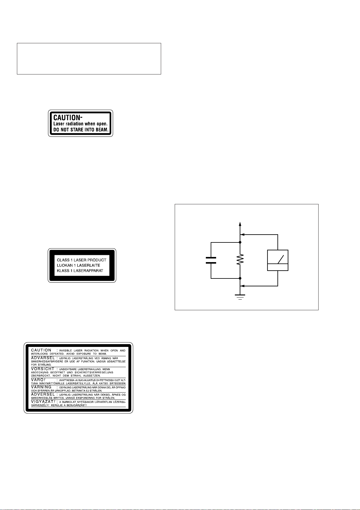
CAUTION
Use of controls or adjustments or performance of procedures
other than those specified herein may result in hazardous radiation exposure.
SAFETY CHECK-OUT
After correcting the original service problem, perform the following safety check before releasing the set to the customer:
Check the antenna terminals, metal trim, “metallized” knobs,
screws, and all other exposed metal parts for AC leakage.
Check leakage as described below.
The following caution label is located
inside of the unit.
For the customers in Canada
CAUTION
TO PREVENT ELECTRIC SHOCK, DO
NOT USE THIS POLARIZED AC PLUG
WITH AN EXTENSION CORD,
RECEPTACLE OR OTHER OUTLET
UNLESS THE BLADES CAN BE FULLY
INSERTED TO PREVENT BLADE
EXPOSURE.
For the customers in Europe
This appliance is classified as a CLASS 1
LASER product.
The CLASS 1 LASER PRODUCT
MARKING is located on the rear exterior.
LEAKAGE TEST
The AC leakage from any exposed metal part to earth ground and
from all exposed metal parts to any exposed metal part having a
return to chassis, must not exceed 0.5 mA (500 microamperes.).
Leakage current can be measured by any one of three methods.
1. A commercial leakage tester , such as the Simpson 229 or RCA
WT -540A. Follo w the manufacturers’ instructions to use these
instruments.
2. A battery-operated AC milliammeter. The Data Precision 245
digital multimeter is suitable for this job.
3. Measuring the voltage drop across a resistor by means of a
VOM or battery-operated AC voltmeter. The “limit” indication is 0.75 V, so analog meters must have an accurate lowvoltage scale. The Simpson 250 and Sanwa SH-63Trd are examples of a passive VOM that is suitable. Nearly all battery
operated digital multimeters that have a 2 V A C range are suitable. (See Fig. A)
To Exposed Metal
Parts on Set
AC
0.15 µF
1.5 k
Ω
voltmeter
(0.75 V)
Laser component in this product is capable of emitting radiation
exceeding the limit for Class 1.
The following caution label is located inside the unit.
SAFETY-RELATED COMPONENT WARNING!!
COMPONENTS IDENTIFIED BY MARK 0 OR DOTTED
LINE WITH MARK 0 ON THE SCHEMATIC DIAGRAMS
AND IN THE PARTS LIST ARE CRITICAL TO SAFE
OPERATION. REPLACE THESE COMPONENTS WITH
SONY PARTS WHOSE PART NUMBERS APPEAR AS
SHOWN IN THIS MANUAL OR IN SUPPLEMENTS PUBLISHED BY SONY.
Earth Ground
Fig. A. Using an AC voltmeter to check AC leakage.
Notes on chip component replacement
• Never reuse a disconnected chip component.
• Notice that the minus side of a tantalum capacitor may be damaged by heat.
Flexible Circuit Board Repairing
• Keep the temperature of the soldering iron around 270 ˚C during repairing.
• Do not touch the soldering iron on the same conductor of the
circuit board (within 3 times).
• Be careful not to apply force on the conductor when soldering
or unsoldering.
ATTENTION AU COMPOSANT AYANT RAPPORT
À LA SÉCURITÉ!
LES COMPOSANTS IDENTIFIÉS P AR UNE MARQUE 0
SUR LES DIAGRAMMES SCHÉMATIQUES ET LA LISTE
DES PIÈCES SONT CRITIQUES POUR LA SÉCURITÉ
DE FONCTIONNEMENT. NE REMPLACER CES COMPOSANTS QUE PAR DES PIÈCES SONY DONT LES
NUMÉROS SONT DONNÉS DANS CE MANUEL OU
DANS LES SUPPLÉMENTS PUBLIÉS PAR SONY.
2

SECTION 3
t
SERVICING NOTES
NOTES ON HANDLING THE OPTICAL PICK-UP
BLOCK OR BASE UNIT
The laser diode in the optical pick-up block may suffer electrostatic break-down because of the potential difference generated
by the charged electrostatic load, etc. on clothing and the human
body.
During repair, pay attention to electrostatic break-down and also
use the procedure in the printed matter which is included in the
repair parts.
The flexible board is easily damaged and should be handled with
care.
NOTES ON LASER DIODE EMISSION CHECK
The laser beam on this model is concentrated so as to be focused
on the disc reflective surface by the objective lens in the optical
pick-up block. Therefore, when checking the laser diode emission, observe from more than 30 cm away from the objecti ve lens.
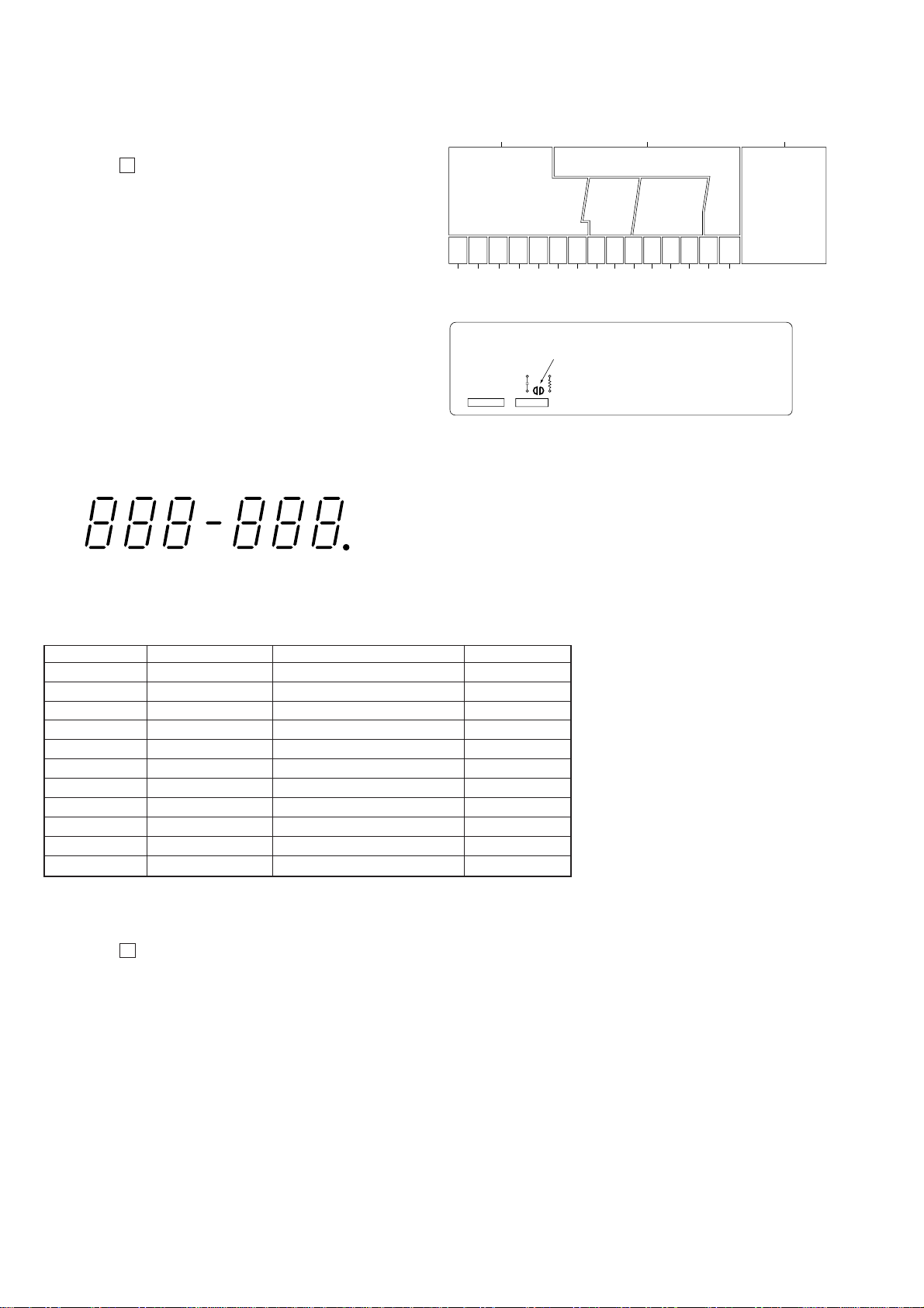
MODEL IDENTIFICATION
– Back Panel –
CHECKING METHOD OF MICROCOMPUTER ROM
VERSION
1. Set the CD1/CD2 switch on the remote commander to CD1.
2. With the power turned on, press the [CHECK] button on the
remote commander while pressing the [TEXT] button on the
set.
3. 15-digit numeric value will be displayed, and the top 4 digits
(left side) of the numeric value imply the microcomputer ROM
version.
Example: If “200006100FFFF3C” is displayed, the ROM ver sion is 2.000.
4. To cancel the ROM version check mode, press the [CHECK]
button on the remote commander while pressing the [TEXT]
button on the set.
DISPLAY OF TOC ERROR
Display Contents
TOC ERROR
TOC ERROR
Illegal SACD disc (pirate edition)
****
Not SACD (DVD disc etc.)
*
Part No.
Model Part No.
SCD-1: US, Canadian 4-215-784-1
SCD-1: AEP 4-215-784-2
SCD-777ES: AEP 4-221-854-0
SCD-777ES: US, Canadian 4-221-854-1
s
s
s
s
SERVICE POSITION
In checking the BU section, prepare two new jigs (extension cable J-2501-164-A: 1.00 mm 26 cores).
OP mechanism section (BU-23)
insulator
connect two jigs (extension cable J-2501-164-A) to the RF board
(CN001, 002) and Main board (CN501, 502).
Any board to pu
3
REPLACING OPTICAL PICK-UP
Handling
1) A red laser diode for Super Audio CD Player requires more
attention to static electricity than general infrared laser diodes
for CD.
Because its durability to static electricity is far weaker than
that of infrared laser diodes, always use an earth band when
handling the optical pick-up block as service parts.
2) As for the flexible board KHS-180A (RP) packed as service
parts, the short lands have been soldered to protect from static
electricity. Accordingly, remove solders when replacing optical pick-up. (See Fig. 1)
DVD short land
3) In handling the KHS-180A (RP), do not touch inhibited parts
shown in Fig. 2, but grip the slide base bearing and U-shaped
guide.
Slide base bearing
Skew sensor
Lens actuator
covers
Objective lenses
CD short land
Fig. 1 Flexible board
Laser holder
U-shaped guide
OEIC
Touch inhibited parts
• Objective lens
• Skew sensor
• Laser holder
• Laser coupler
• Flexible board
• OEIC
• Lens actuator covers
Flexible board
Connector
Laser coupler
Fig. 2 KHS-180A (RP)
4
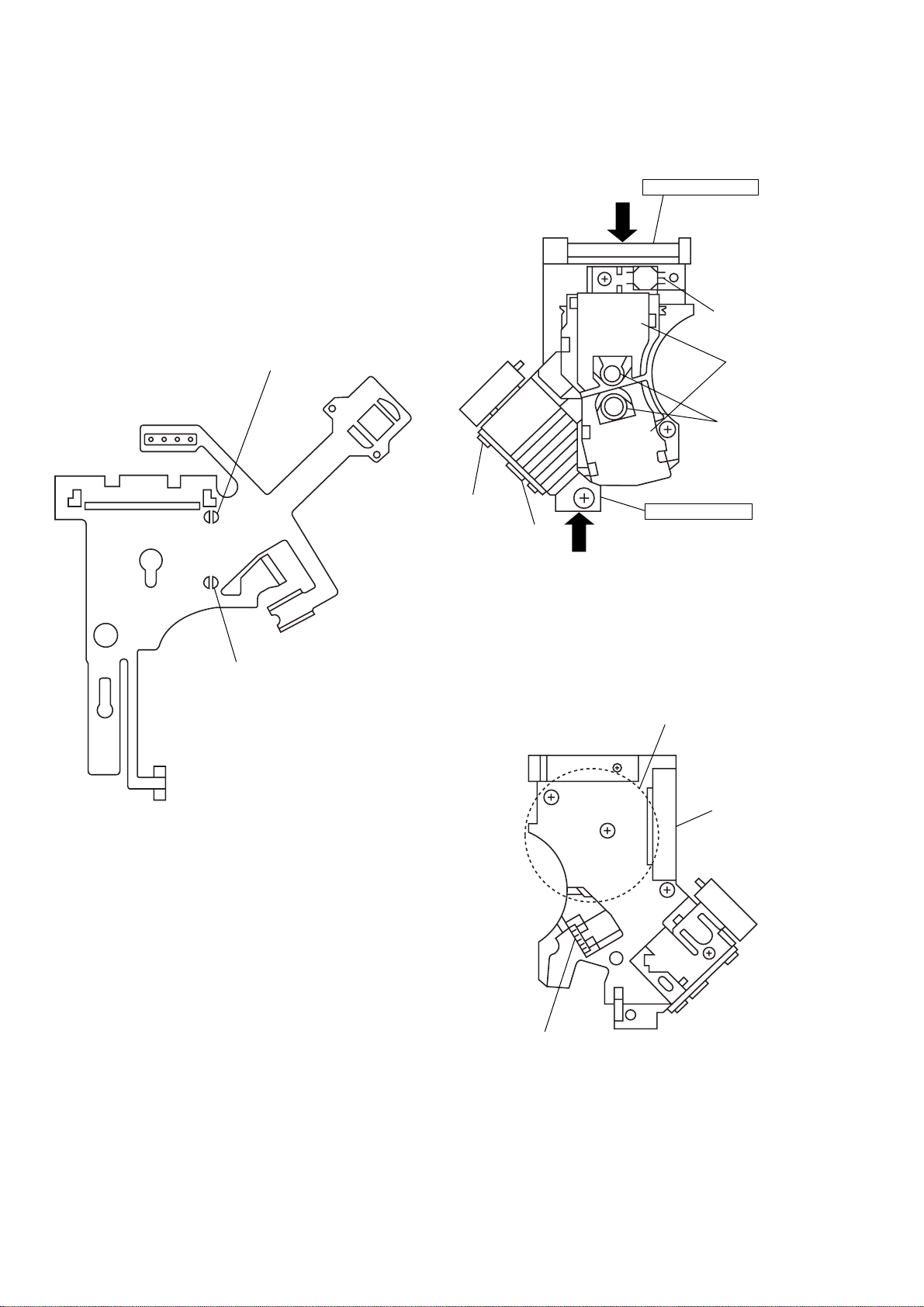
SECTION 4
OPTICAL PICK-UP
(KHS-180A/J1N) (Page 7)
RF BOARD (Page 7)
DISASSEMBLY-2
Note: Follow the disassembly procedure in the numerical order given.
OP MECHANISM SECTION (BU-23)
3
two screws
(B2.6
×
5)
4
4
1
screw (PS3 × 5)
two washers
2
lag
two washers
3
two screws
(B2.6
×
5)
5
Lift up OP mechanism section (BU-23).
6
two wires (flat type) (26 core)
(CN501, 502)
MAIN BOARD
3
MAIN board
2
five screws
(PS 3
1
two connectors
×
5)
(CN701, 708)
1
five connectors
(CN702-706)
5

s
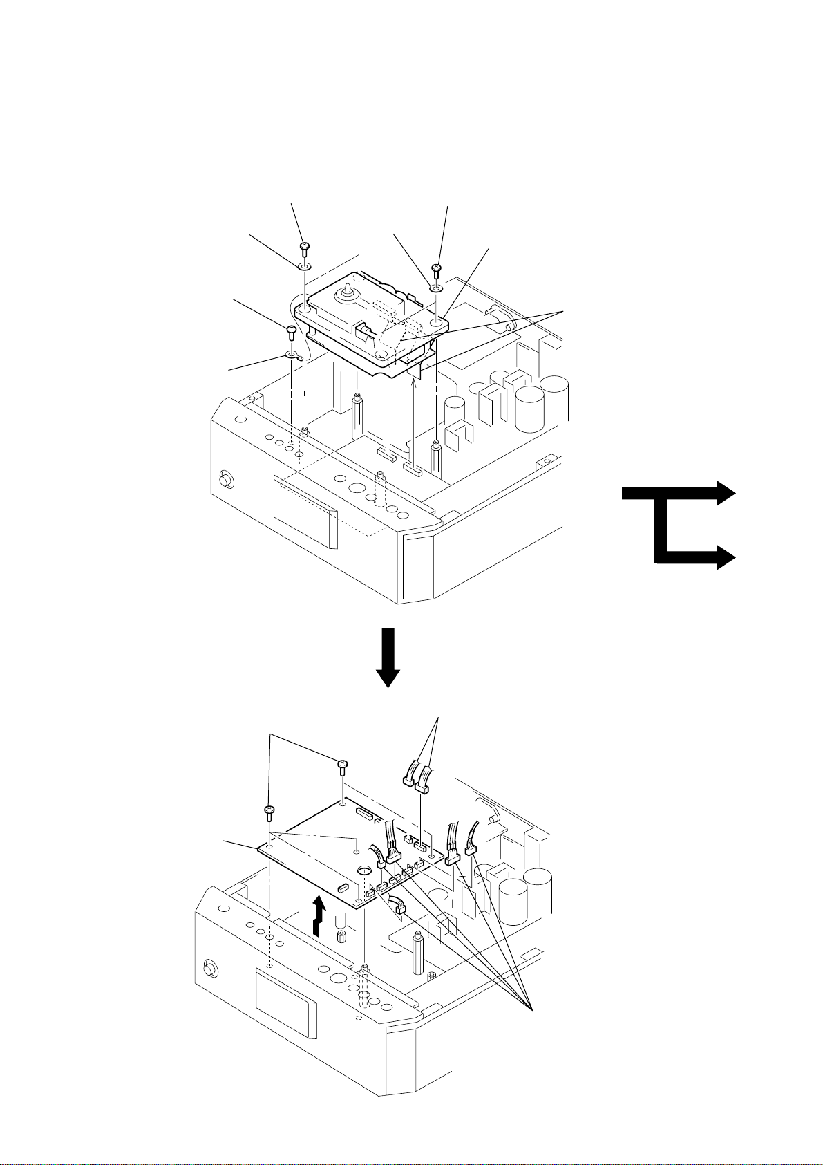
FRONT PANEL SECTION (SCD-1)
4
six screws
×
8)
(RK4
5
side plate (L)
7
two screws
×
(BVTT4
6)
3
push (control block) (wire) switch
8
front panel section
6
five screws
(BVTP3
×
5
10)
side plate (R)
2
two claws
2
1
4
six screws
(RK4
two claws
two connectors
(CN452, 702)
×
8)
FRONT PANEL SECTION (SCD-777ES)
4
six screws
(RK4
×
8)
5
side plate (R)
7
screw (BVTT3 × 6)
8
front panel section
3
push (control block) (wire) switch
2
two claws
2
two claws
1
two connectors
(CN452, 702)
4
six screw
(RK4 × 8)
7
screw (BVTT3 × 6)
6
four screws
(BVTP3
×
10)
5
side plate (L)
6

OPTICAL PICK-UP (KHS-180A/J1N)
y
)
2
3
holder (R2)
4
holder (R)
5
bracket (OP) ass'y
1
OP-15 flexible print board
(CN003)
screw
(PSW3
×
10)
6
two screws (B3 × 5)
9
7
retainer (OP) ass'
8
leaf spring (Y)
optical pick-up
(KHS-180A/J1N)
RF BOARD
1
OP-15 flexible print board
(CN003)
5
RF board
4
four spacers (3 × 5)
3
four screws
(B3
×
10)
2
connector
(CN005)
1
wire (flat type) (14 core
(CN007)
2
two connectors
(CN004, 006)
7

SLED MOTOR ASS'Y SECTION
d
1
2
cover (BU)
five screws
(B3 × 5)
3
three poly-slider washers
4
gear (D)
5
6
gear (B)
gear (C)
0
sled motor ass'y section
TILT MOTOR ASS'Y (M3)
2
bracket (tilt) ass'y
9
three screws
(B3 × 5)
7
8
SLD-MOT boar
screw
(B3 × 5)
4
tilt motor ass'y (M3)
3
two precision screws
(P2
×
2.5)
1
two screws
(B3
×
5)
8
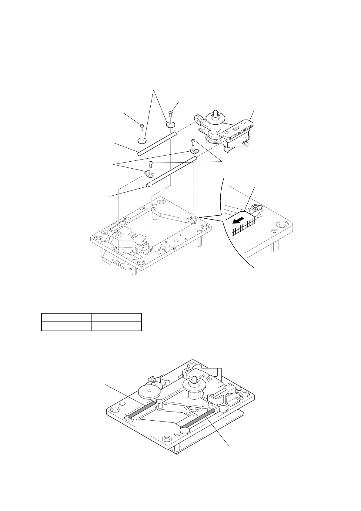
SPINDLE MOTOR BLOCK
2
screw
(B3
6
sled shaft (sub)
4
two shaft retainers (main)
7
sled shaft (main)
3
two shaft retainers (sub)
×
5)
2
screw
(B3
×
5)
2
two screws
(B3
5
spindle motor block
×
5)
1
slide the spindle motor block
toward the arrow.
APPLYING OIL AT REPLACEMENT OF MOTOR (SPINDLE) (M7)
When replacing the motor (spindle) (M7), apply a drop of oil to the
sled shaft (sub) and the sled shaft (main) respectively.
Part Name Part No
FLOIL (946P) 7-662-001-37
Notes:
• Do not attach oil to other than specified parts.
• Do not touch the lens and laser diode during work.
sled shaft (main)
sled shaft (sub)
9
SECTION 5
TEST MODE
5-1. FLUORESCENT INDICATOR TUBE MODE
Note: Set the CD1/CD2 switch on the remote commander to CD1.
Procedure:
1. Press the ! button while shorting the BP (TEST MODE) on
the DISPLA Y board with tweezers, etc. and turn on the po wer,
so that the following operation will be executed automatically.
(1) All segments from 1G to 19G light up in order, starting from
1G.
(2) Vertical one line (total 7) of all grids from 1G to 15G lights up
in order, starting from the left.
(3) Horizontal one line (total 5) of all grids from 1G to 15G lights
up in order, starting from the top.
(4) Grids from 1G to 15G go off, and all segments from 16G to
19G light up.
2. With the set in the 1-(4) status, pressing any ke y on the remote
commander changes the display as shown below , and acti vates
the key check standby mode.
ARTIST
STEP
INDEX
CD1 CD2 CD3
MIN
Geid Assignment
16G 19G 20G
18G17G
1G 2G 3G 4G 5G 6G 7G 8G 9G 10G 11G 12G 13G 14G 15G
– DISPLAY Board (Conductor Side) –
BP (TEST MODE)
CN1002
CN1001
3. When a key on the front panel is pressed, the corresponding
segment and LED light up. (See table below)
key on set Key Attribute Lighting segment (in 19 grids) Lightning LED
A EJECT 20 bit –
TIME TIME 24 bit –
TEXT TEXT __|_____ (DIGITAL FILTER) –
DIGITAL OUT DIGITAL OUT DIGITAL OUTPUT –
FILTER FILTER __|_____ (DIGITAL OUTPUT) –
SACD/CD SACD/CD NORM –
H PLAY WIDE PLAY LED
X PAUSE STD1234 PAUSE LED
x STOP DIGITAL FILTER –
l AMS-BACK 16 bit CD LED
L AMS-FORWARD OFF SACD LED
4. If “!%%TEST-END!!%%” is displayed after the keys listed
above were all pressed, the key check terminated successfully .
Note: As this test does not check the LEDs, check them visually.
5. Press the ! button to turn the power off, and disconnect the
plug from the socket.
10

5-2. ADJUSTMENT-1 MODE
This mode is a special mode used to perform overall adjustment,
optical pick-up height adjustment, and service check.
Note:
1. Wrong setting method can cause a trouble.
2. Never operate the set with the loading panel mounted, which otherwise
causes a trouble.
Setting Method:
1. With the power turned of f, press the ! button while pressing
the [DIGITAL OUT] button and l button.
2. Display of “bbb” implies that the set is now in the Adjust-
ment-1 Mode.
Resetting Method:
Press the ! button to turn the power off, and disconnect the plug
from the socket.
5-3. ADJUSTMENT-2 MODE
This mode is a special mode used to perform CL V jitter check and
usually movement check.
Note:
1. Wrong setting method can cause a trouble.
2. Never operate the set with the loading panel mounted, which otherwise
causes a trouble.
Setting Method:
1. With the power turned of f, press the ! button while pressing
the [TIME] button and H button.
2. Display of “# OPEN #” implies that the set is now in the Ad-
justment-2 Mode.
Resetting Method:
Press the
! button to turn the power off, and disconnect the plug
from the socket.
Adjustment item
Traverse check, S curve check,
Adjustment-1 RF level check, optical pick-up
Mode height adjustment, and see contents of
Adjustment-1 Mode list.
Adjustment-2 CLV jitter check and usually
Mode movemant check
Adjustment-1 Mode List
Note: Set the CD1/CD2 switch on the remote commander to CD1.
Codes Contents Remarks Disc
01 LD ON/OFF CD, SL, DL
02 Spindle ON/OFF CD, SL, DL
03 Forcus Search CD, SL, DL
04 Forcus Servo ON/OFF CD, SL, DL
05 Track Servo ON/OFF CD, SL, DL
06 CLV ON CD, SL, DL
07 Sled Servo ON/OFF CD, SL, DL
22 Tilt Servo ON/OFF CD, SL, DL
23 Tilt Bias Up CD, SL, DL
24 Tilt Bias Down CD, SL, DL
30 Disc Check CD, SL, DL
5: Thresholds
check
60 Overall Adjustment 9: No thresholds CD, SL, DL
61 Result Display
62 Adj. V alue Clear
PLAY PLAY CD, SL, DL
PAUSE PAUSE CD, SL, DL
STOP STOP CD, SL, DL
NEXT NEXT CD, SL, DL
PREV PREV CD, SL, DL
FILTER Focus Search/PLAY
Note:
1. Selection of an adjustment item where no disc is present could damage
the optical pick-up.
2. Do not use other than above listed codes.
check
0: Cancel
1: Proceed
2: Return
9: Go
0: Cancel
SACD select
(SACD/CD key)
CD select
(SACD/CD key)
Go
CD, SL, DL
CD, SL, DL
SL
CD
*1: Disc check list
Display Result of Disc Check
Discchk DO SL No disc
Discchk D1 SL SL
Discchk D2 CD CD
Discchk D3 CD Hybrid CD layer
Discchk D3 HD Hybrid HD layer
Discchk D4 D0 DL L0 layer
Discchk D4 D1 DL L1 layer
*1
11

SECTION 6
ELECTRICAL ADJUSTMENTS
Note on Adjustment
1. When the following parts were replaced, adjust and check the
items marked with a in the given order.
Parts
Adjustment & check pick-up MAIN board motor (M7)
1. Optical Pick-up
Height Adjustment
2. Overall Adjustment aa ×
3. Traverse Check a ××
4. S Curve Check a ××
5. RF Level Check a ××
6. CLV Jitter Check ×× a
Optical IC on RF or Spindle
a × a
2. Adjustment jigs
The following jigs are exclusively used for electrical adjustment and check of this set. Do not use them for other applications.
(1) Disc
Model Type*1 Category Applications
SATD-S1 SL 8cm disc Optical pic-kup H adj.
SATD-S2 SL Reference disc Overall adj. and check
SATD-S3 DL Reference disc Overall adj. and check
SATD-S4 SL Reference disc Audio characteristic check
TCD-784 CD Reference disc Overall adj. and check
*1 SL: Single Layer
DL: Dual Layer
(2) Remote commander: Assessory for set or RM-D950 (Part No.
1-473-944-1)
(3) Extension cable (Part No. J-2501-164-A) 2 pcs.
3. In making adjustment and check, set the CD1/CD2 switch on
the remote commander to CD1.
4. The impedance of oscilloscope should be more than 10M .
Traverse Check
Connection:
oscilloscope
(auto or normal mode)
MAIN board
TP516 (TE)
TP501 (VC)
+
–
Procedure:
1. Connect an oscilloscope to the TP516(TE) and TP501(VC) on
the MAIN board.
2. Set the Adjustment-1 Mode. (See 5-2. Adjustment-1 Mode in
SECTION 5 (page 11))
3. Set a disc (SATD-S2, SATD-S3, or TCD-784).
4. Press the 3 button and - button on the remote commander
to make the disc type checked.
Note: If the disc check was made in the Adjustment-1 Mode, pressing
another button immediately after pressing the 3 and - buttons
on the remote commander could cause the microcomputer to run
out of control, thus requiring extreme care.
5. Confirm that the disc was checked.
bbb
CD1
Discchk XX XX
Disc type (refer to Disc check list (page 11))
6. Press the H button.
7. Press the - button and 7 button, and the - button and 5
button on the remote commander successively to turn off the
tracking servo.
8. Check that the waveform on oscilloscope is within the level
A and B specifications.
9. After checking, press the x button.
10. Repeat steps 3 through 9 respective discs.
11. Press the ! button to turn the power off.
Specified Value:
Disc A
SATD-S2
SATD-S3 1.3 to 2.4 Vp-p - 0.1 to +0.1 V
TCD-784
B
12
Traverse waveform
VC
Adjustment Location : See page16.
Center fo the waveform
A
B
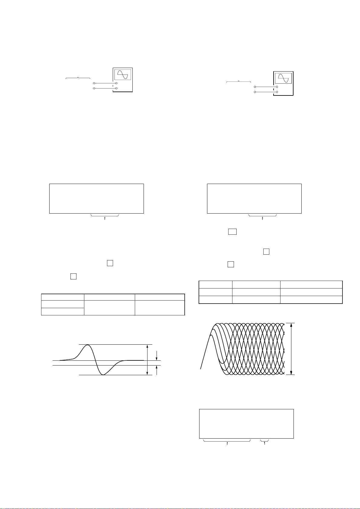
S Curve Check
)
MAIN board
TP503 (RF)
TP501 (VC)
+
–
oscilloscope
(auto mode)
VOLT/DIV: 200 mV
TIME/DIV: 500 ns
RF signal waveform
A
Connection:
MAIN board
TP524 (FE)
TP501 (VC)
RF Level Check
Connection:
oscilloscope
(normal mode
+
–
Procedure:
1. Connect an oscilloscope to the TP524(FE) and TP501(VC) on
the MAIN board.
2. Set the Adjustment-1 Mode. (See 5-2. Adjustment-1 Mode in
SECTION 5 (page 11))
3. Set a disc (SATD-S2 or TCD-784).
4. Press the 3 button and - button on the remote commander
to make the disc type checked.
Note: If the disc check was made in the Adjustment-1 Mode, pressing
another button immediately after pressing the 3 and - buttons
on the remote commander could cause the microcomputer to run
out of control, thus requiring extreme care.
5. Confirm that the disc was checked.
bbb
CD1
Discchk XX XX
Disc type (refer to Disc check list (page 11))
6. Press the - button and 1 button, the - button and 2 button, and the - button and 3 button on the remote commander
successively to execute the focus search.
7. Check that the waveform on oscilloscope is within the level
A and B specifications.
8. After checking, press the x button.
9. Repeat steps 3 through 8 for respective discs.
10. Press the ! button to turn the power off.
Specified V alue:
Disc
SA TD-S2
TCD-784
AB
1.5 to 2.3Vp-p - 0.1 to +0.1V
Procedure:
1. Connect an oscilloscope to the TP503(RF) and TP501(VC) on
the MAIN board.
2. Set the Adjustment-1 Mode. (See 5-2. Adjustment-1 Mode in
SECTION 5 (page 11))
3. Set a disc (SATD-S2 or TCD-784).
4. Press the 3 button and - button on the remote commander
to make the disc type checked.
Note: If the disc check was made in the Adjustment-1 Mode, pressing
another button immediately after pressing the 3 and - buttons
on the remote commander could cause the microcomputer to run
out of control, thus requiring extreme care.
5. Confirm that the disc was checked.
bbb
CD1
Discchk XX XX
Disc type (refer to Disc check list (page 11))
6. Press the H button.
7. Check that the waveform on oscilloscope is clear, and the le vel
and jitter of waveform satisfy the specifications.
8. After checking, press the x button.
9. Repeat steps 3 through 8 for respective discs.
10. Press the ! button to turn the power off.
Specified Value:
Disc A Jitter (displayed value)
SATD-S2 1.25 to 1.65 Vp-p 20 (Hex) or less
TCD-784 1.3 to 1.7 Vp-p 15 (Hex) or less
S curve waveform
A
VC
Note: For easier observation of this waveform, extend the sweep time
and raise the brightness.
B
Adjustment Location : See page16.
Note: Clear RF waveform refers to the waveform where ◊ shapes should
be distinctively observed in the center.
Display example:
bbb
CD1
+ 00 00 ~00 09
not fixed
Jitter value
(HEX)
Adjustment Location : See page16.
13
)
CLV Jitter Check
w
Connection:
MAIN board
TP702 (MNT4)
TP703 (MNT5)
TP521 (GND)
(normal mode
(CH2)
(CH1)
oscilloscope
+ +
–
Optical Pick-up Height Adjustment
Connection:
TP511 (FOUT)
MAIN board
TP515 (PI)
TP501 (VC)
(CH1)
(CH2)
storage
oscilloscope
(normal mode)
+
+
–
Procedure:
1. Connect an oscilloscope to the TP702(MNT4)(CH1),
TP703(MNT5)(CH2) and TP521(GND) on the MAIN board.
2. Set the Adjustment-2 Mode. (See 5-3. Adjustment-2 Mode in
SECTION 5 (page 11))
3. Set a disc (SATD-S2 or TCD-784).
4. Press the H button.
5. Move the sled to the middle track.
• Sled middle track
SATD-S2:TN05
TCD-784:TN05
6. Check that the A value of waveform on oscilloscope satisf ies
the specification.
7. After checking, press the x button.
8. Repeat steps 3 through 7 for respective discs.
9. Press the ! button to turn the power off.
Specified Value:
Disc A
SATD-S2
TCD-784
CLV jitter waveform
55 µsec or less
Procedure:
1. Connect an oscilloscope to the TP515(PI)(CH1),
TP511(FOUT) (CH2) and TP501(VC) on the MAIN board.
2. Set the Adjustment-1 Mode. (See 5-2. Adjustment-1 Mode in
SECTION 5 (page 11))
3. Set a disc (SATD-S1).
4. Press the [FILTER] button to set the Focus Search mode.
5. Loosen the OP height adjusting screw 1, and while shifting
the Holder (R2), adjust the height so that the waveform on
oscilloscope satisfies the specified value.
6. Press the [FILTER] button to set the Play mode.
7. Adjust the TAN skew 2 so as to attain most preferable jitter
value on the display.
8. Press the [FILTER] button to set the Focus Search mode.
9. Check that the B value of waveform on oscilloscope satisf ies
the specification.
10. Repeat steps 5 through 9.
11. Lock the OP height adjusting screw 1 when adjustment finished.
12. Press the x button.
13. Press the ! button to turn the power off.
Specified Value: B is more than 0, and less than A/3
B
Adjustment Location : See page16.
A
VC
A
VC
PI
FOUT
*1: Normal-trigger the oscilloscope using FOUT on CH2.
2
TAN skew
1
OP height
adjusting scre
*1
14
Adjustment Location : See page16.
Holder (R2)

Overall Adjustment
Procedure:
1. Set the Adjustment-1 Mode. (See 5-2. Adjustment-1 Mode in
SECTION 5 (page 11))
2. Press the 6 button and 2 button, then the 9 button on the
remote commander (to initialize data).
3. Set a disc (TCD-784).
4. Press the 6 button and - button, then the 5 button on the
remote commander. (Adjustment will take about 2 minutes.)
5. Remove the disc when "CD END" is displayed.
6. Set a disc (SATD-S2).
7. Press the 6 button and - button, then the 5 button on the
remote commander. (Adjustment will take about 1 minute 30
seconds.)
8. Remove the disc when "SL END" is displayed.
9. Set a disc (SATD-S3).
10. Press the 6 button and - button, then the 5 button on the
remote commander. (Adjustment will take about 1 minute.)
11. Remove the disc when "DL END" is displayed.
Note: If an error is displayed during the adjustment so far, press again the
6 button and - button on the remote commander to execute readjustment.
12. Press the 6 button and 1 button on the remote commander.
13. As the number and adjusted value are displayed, make sure
that it is within the threshold.
14. Press the 1 button on the remote commander to proceed to
the next item. (To return to the previous item, press the 2
button.)
15. Repeat steps 13 and 14.
16. After checking items up to No.43, press the ! button to turn
the power off.
Thresholds for Overall Adjustment
No. Description U limit L limit
00 PI Level SL 0 4
01 PI Level DL 3 7
02 PI Offset CD 15D 2A3
03 PI Offset SL 15D 2A3
04 PI Offset DL 15D 2A3
05 PI Offset Disc Check 100 2FF
06 Traverse Offset CD
07 Traverse Offset SL
08 Traverse Offset DL
09 Traverse Gain CD
10 Traverse Gain SL
11 Traverse Gain DL
12 For PI Level Disc Check 0 2
13 PI Reflectance SL 2D28 7333
14 PI Reflectance DL 936 4083
15 Surface Reflect to CD Layer Distance 82
16 Surface Reflect to DSD Layer Distance 41 82
17 Low Push-pull for Disc Check 4FDF 9999
18 High T Bal for Disc Check 0000 47AE
19 FE Offset CD
20 FE Offset SL
21 FE Offset DL
22 Focus Bias CD E0 20
23 Focus Bias SL E0 20
24 Focus Bias DL0 E0 20
25 AGC Focus Gain CD 1500 3000
26 AGC Focus Gain DL 0851 1A00
27 AGC Focus Gain SL 0C28 2500
28 AGC Tracking Gain CD 1A00 3C00
29 AGC Tracking Gain SL 1100 2500
30 AGC Tracking Gain DL 1400 2700
31 RF Loop Filter Offset CD F6 0A
32 RF Loop Filter Offset DSD F6 0A
33 Tilt Disordered Point CD +side
34 Tilt Disordered Point CD -side
35 Tilt Disordered Point SL +side
36 Tilt Disordered Point SL -side
37 Tilt Disordered Point DL +side
38 Tilt Disordered Point DL -side/
39 Tilt Offset CD F0 10
40 Tilt Offset SL F0 10
41 Tilt Offset DL F0 10
42 Focus Balance SL
43 Focus Balance DL
Note: 1. No threshold specified for items.
2. All thresholds are displayed in Hex.
15

Adjustment Location:
– MAIN Board (Component Side) –
TP524
(FE)
TP501
TP521
(GND)
(VC)
TP503
(RF)
TP703
(MNT5)
TP511
(FOUT)
TP515
(PI)
TP516
(TE)
TP702
(MNT4)
16
SECTION 7
)
d
DIAGRAMS
7-1. NOTES FOR PRINTED WIRING BOARD AND SCHEMATIC DIAGRAM
Note on Printed Wiring Board:
• X : parts extracted from the component side.
• Y : parts extracted from the conductor side.
a
•
• b : Pattern from the side which enables seeing.
(The other layers' patterns are not indicated.)
Caution:
Pattern face side: Parts on the pattern face side seen from
(Conductor Side) the pattern face are indicated.
Parts face side: Parts on the par ts face side seen from
(Component Side) the parts face are indicated.
• Indication of transistor
: Through hole.
C
Q
B
E
These are omitted.
Note on Schematic Diagram:
• All capacitors are in µF unless otherwise noted. pF: µµF
50 WV or less are not indicated except for electrolytics
and tantalums.
• All resistors are in Ω and 1/
specified.
• % : indicates tolerance.
f
•
• 5 : fusible resistor.
• C : panel designation.
Note:
The components identified by mark 0 or dotted
line with mark 0 are critical for safety.
Replace only with part
number specified.
• U : B+ Line.
• V : B– Line.
• Voltages and wav eforms are dc with respect to ground in
• Voltages are taken with a VOM (Input impedance 10 MΩ).
• Waveforms are taken with a oscilloscope.
• Circled numbers refer to waveforms.
• Signal path.
: internal component.
adjustment mode.
no mark :STOP
( ) :SACD
〈〈 〉〉 :CD
Voltage variations may be noted due to normal production tolerances.
Voltage variations may be noted due to normal production tolerances.
J : SACD
c : CD
I : DIGITAL OUT
4
W or less unless otherwise
Note:
Les composants identifiés par
une marque 0 sont critiques
pour la sécurité.
Ne les remplacer que par une
pièce portant le numéro
spécifié.
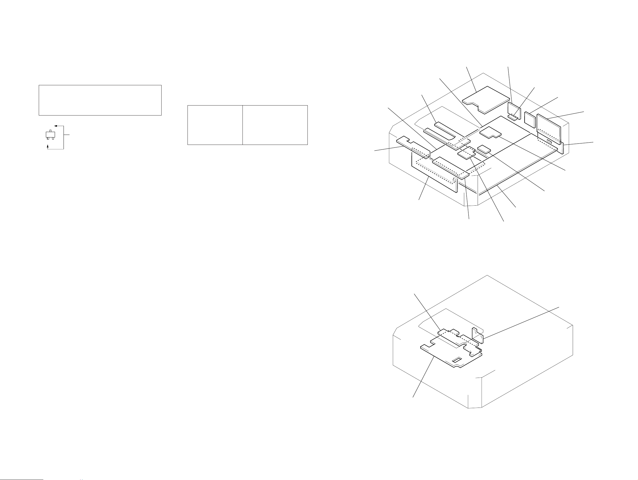
• Circuit Boards Location
MAIN board
SW-L board
DISPLAY board
POWER board
STB board
AC board
SW-R board
COAX board
OPT board
SW board
BAL board (SCD-1
PIN board
LOAD-SW board
LOAD-MOT board
AUDIO board
LOAD-CN board
SLD-MOT board
SLD-FG boar
RF board
1717

SCD-1/777ES
7-2. PRINTED WIRING BOARDS – RF/SLD-FG/SLD-MOT Boards – • See page 17 for Circuit Boards Location.
(Page 22)
(Page 22)
• Semiconductor Location
–RF Board–
Ref. No. LocationRef. No. Location
IC001 E-2
IC002 C-4
IC003 A-3
IC004 A-2
IC005 C-3
IC006 C-3
IC007 C-2
IC010 A-2
IC011 C-2
IC012 A-1
Q001 F-3
Q002 B-5
Q003 B-4
Ref. No. Location
Q004 B-4
Q006 A-3
Q007 D-5
Q008 B-5
Q009 B-5
1818

7-3. SCHEMATIC DIAGRAM – RF/SLD-FG/SLD-MOT Boards – • See page 40 for Waveforms.
SCD-1/777ES
(Page
29)
The components identified by mark 0 or dotted
line with mark 0 are critical for safety.
Replace only with part number specified.
(Page
28)
Les composants identifiés par une marque 0 sont
critiques pour la sécurité. Ne les remplacer que
par une pièce portant le numéro spécifié.
1919
SCD-1/777ES
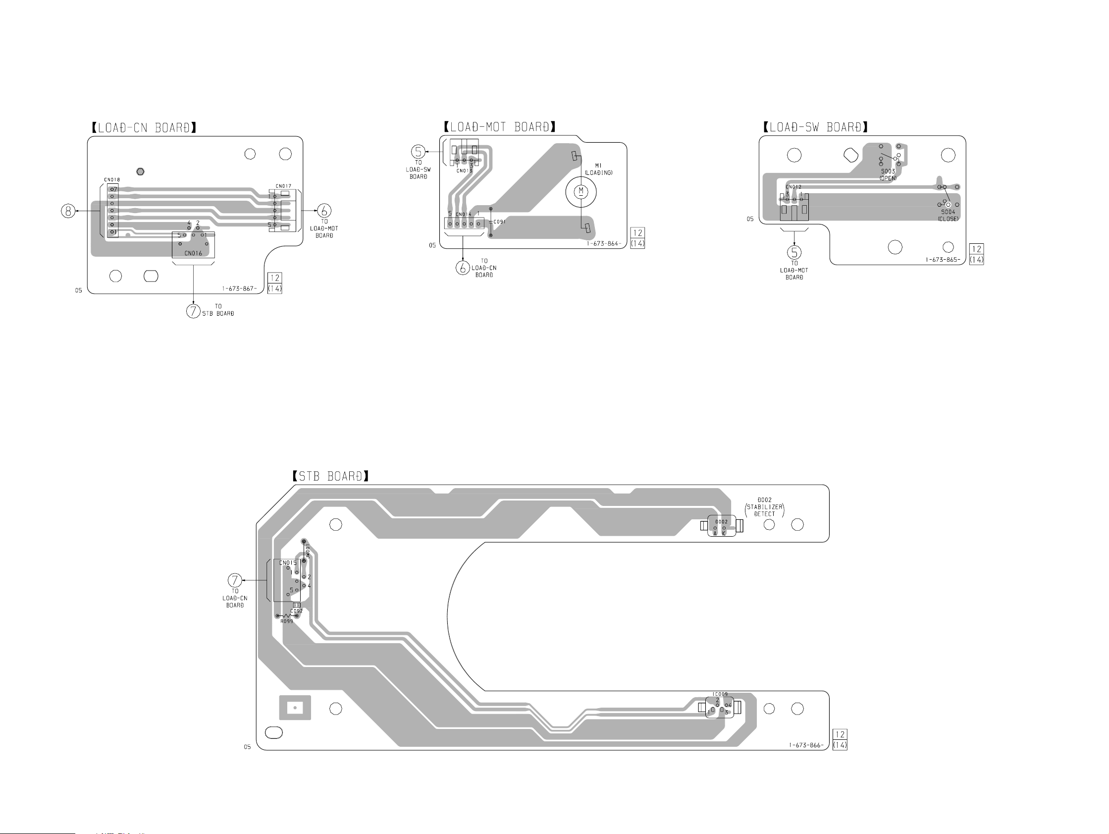
7-4. PRINTED WIRING BOARDS – LOAD-CN/LOAD-MOT/LOAD-SW/STB Boards – • See page 17 for Circuit Boards Location.
(Page 22)
2020
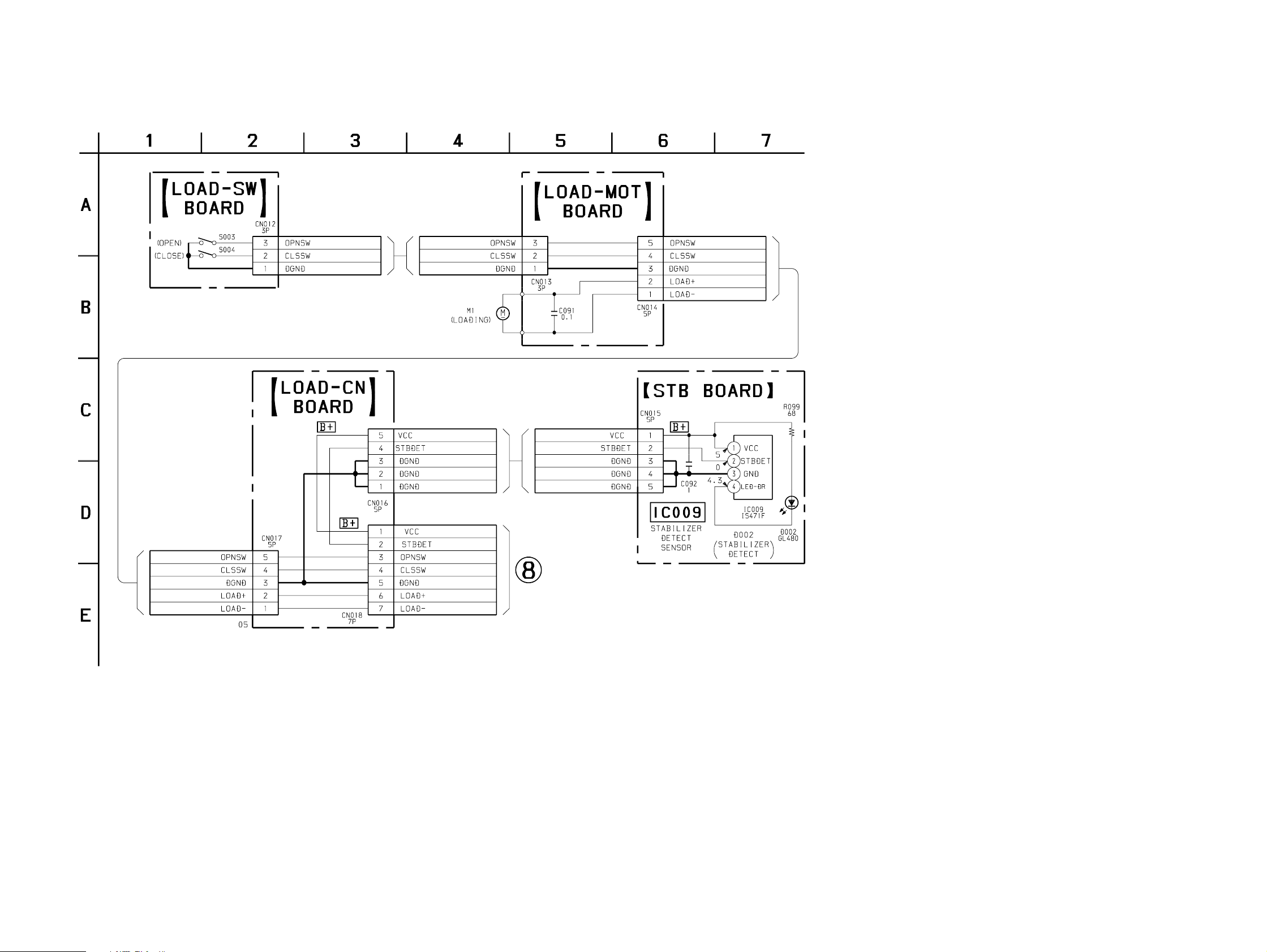
7-5. SCHEMATIC DIAGRAM – LOAD-CN/LOAD-MOT/LOAD-SW/STB Boards –
SCD-1/777ES
(Page 29)
2121

SCD-1/777ES
7-6. PRINTED WIRING BOARD – MAIN Board (component side) – • See page 17 for Circuit Boards Location.
• Semiconductor
Location
Ref. No. Location
D501 E-5
D502 D-4
D503 E-5
D702 F-12
IC502 D-3
IC507 G-2
IC509 D-5
IC510 E-4
IC511 E-4
IC513 F-6
IC514 F-5
IC516 L-11
IC517 L-11
IC519 D-6
IC520 E-6
IC521 E-6
IC522 B-2
IC523 D-4
IC701 I-5
IC702 C-9
IC703 E-13
IC708 C-13
IC711 H-2
IC713 F-8
IC714 F-9
IC715 G-10
IC716 L-5
IC717 J-3
IC718 I-3
IC719 D-11
IC720 D-12
IC722 B-12
IC724 B-11
IC727 H-13
IC728 E-9
IC730 F-12
IC732 I-14
IC741 F-11
IC750 D-12
IC760 G-14
IC762 G-14
IC764 H-14
IC766 H-14
IC775 H-6
IC778 D-8
IC1501 D-3
IC1503 F-3
IC1651 D-4
(Page 18) (Page 18)
(Page 38)
(Page 38)
(Page 34)
(Page 31)
(Page 31)
(Page 31)
Q507 B-4
Q509 E-5
Q511 E-6
Q705 F-11
Q1651 C-4
Q1652 C-4
Q1653 D-4
(Page 36)
(Page 20)
2222
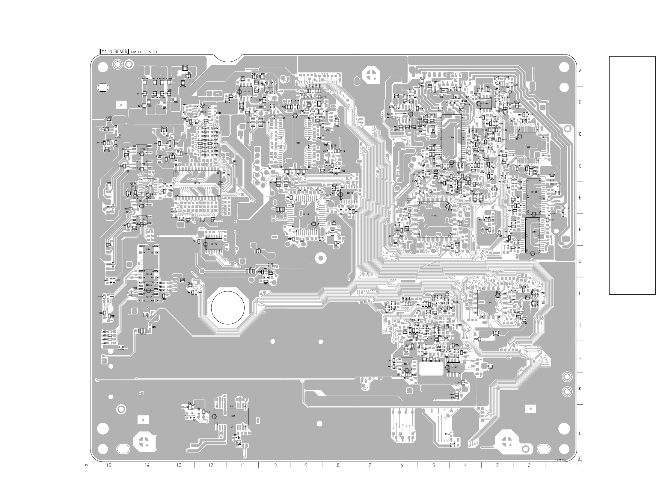
7-7. PRINTED WIRING BOARD – MAIN Board (conductor side) – • See page 17 for Circuit Boards Location.
SCD-1/777ES
• Semiconductor
Location
Ref. No. Location
D504 L-11
D701 C-13
D1501 E-3
IC501 C-2
IC503 E-2
IC504 C-4
IC505 F-2
IC506 B-3
IC508 B-6
IC512 F-5
IC515 L-11
IC707 C-9
IC709 E-12
IC710 F-9
IC712 H-3
IC721 B-11
IC725 E-14
IC726 F-12
IC729 E-8
IC734 J-6
IC735 J-4
IC736 I-5
IC737 I-5
IC739 B-12
IC740 B-10
IC761 G-14
IC763 G-14
IC765 H-14
IC767 H-14
IC770 F-14
IC771 E-14
IC772 C-14
IC773 D-14
IC776 H-2
IC777 H-2
IC1502 B-3
Q501 L-13
Q502 L-13
Q506 C-4
Q508 B-3
2323

SCD-1/777ES
7-8. SCHEMATIC DIAGRAM – MAIN Board (1/7) – • See page 40 for Waveforms.
(Page 28)
(Page 29)
(Page 28)
(Page 39)
(Page 39)
(Page 29)
(Page 25)
(Page 26)
2424
 Loading...