

Page 1

MSM80C154S
MSM83C154S
MSM85C154HVS
USER'S MANUAL
Page 2

Copyright 1988, OKI ELECTRIC INDUSTRY COMPANY, LTD.
OKI makes no warranty for the use of its products and assumes no
responsibility for any errors which may appear in this document nor
does it make a commitment to update the information contained
herein.
OKI retains the right to make changes to these specifications at
any time, without notice.
Page 3

CONTENTS
1. INTRODUCTION
1.1 MSM80C154S/MSM83C154S/MSM85C154HVS Outline ..................................3
1.2 MSM80C154S/MSM83C154S Features.............................................................5
1.3 Additional Features in MSM80C154S/MSM83C154S/MSM85C154HVS...........7
2. SYSTEM CONFIGURATION
2.1 MSM80C154S/MSM83C154S/MSM85C154HVS Logic Symbols ....................11
2.2 MSM80C154S/MSM83C154S Pin Layout ........................................................12
2.2.1 MSM80C154S/MSM83C154S external dimensions..................................15
2.2.2 MSM85C154HVS pin layout and external dimensions..............................17
2.3 MSM80C154S Block Diagram ..........................................................................18
2.4 MSM83C154S Block Diagram ..........................................................................19
2.5 MSM85C154HVS Block Diagram .....................................................................20
2.6 Timing and Control ...........................................................................................21
2.6.1 Outline of MSM80C154S/MSM83C154S timing........................................21
2.6.2 Major synchronizing signals ......................................................................23
(1) ALE ......................................................................................................23
(2) PSEN ...................................................................................................23
(3) WR ...................................................................................................... 23
(4) RD ....................................................................................................... 23
2.6.3 MSM80C154S fundamental operation time charts....................................24
(1) External program memory read cycle timing chart...............................24
(2) MOVX A, @Rr......................................................................................24
(3) MOVX @Rr, A......................................................................................25
(4) MOVX A, @DPTR................................................................................25
(5) MOVX @DPTR, A................................................................................26
(6) MOV direct, PORT[0, 1, 2, 3] execution...............................................26
2.6.4 MSM83C154S fundamental operation time charts....................................27
(1) MOVX A, @Rr......................................................................................27
(2) MOVX @Rr, A..................................................................................... 27
(3) MOVX A, @DPTR................................................................................28
(4) MOVX @DPTR, A................................................................................28
(5) MOV direct, PORT[0, 1, 2, 3] execution...............................................29
2.7 Instruction Register (IR) and Instruction Decoder (PLA) ..................................30
2.8 Arithmetic Operation Section ............................................................................31
(1) Outline..................................................................................................31
(2) Arithmetic operation instruction decoder..............................................31
(3) Arithmetic and logic unit (ALU).............................................................31
2.9 Program Counter ..............................................................................................32
2.10 Program Memory and External Data Memory ..................................................33
2.10.1 MSM80C154S/MSM83C154S program area and
external ROM connections ........................................................................33
2.10.2 Procedures and circuit connections used when external
data memory (RAM) is accessed by data pointer (DPTR) ........................35
2.10.3 Procedures and circuit connections used when external
data memory (RAM) is accessed by registers R0 and R1.........................38
Page 4

3. CONTROL
3.1 Oscillators [XTAL1 .2] .......................................................................................43
3.2 CPU Resetting ..................................................................................................45
3.2.1 Outline .......................................................................................................45
3.2.2 Reset Schmitt trigger circuit.......................................................................50
3.2.3 CPU internal status by reset......................................................................51
3.3 EA(CPU Memory Separate)..............................................................................52
3.3.1 Outline .......................................................................................................52
(1) Internal ROM mode..............................................................................52
(2) External ROM mode.............................................................................52
4. INTERNAL SPECIFICATIONS
4.1 Internal Data Memory (RAM) and Special Function Registers .........................55
4.1.1 Outline ..........................................................................................................55
4.2 Internal Data Memory (RAM)............................................................................57
4.2.1 Internal data memory (RAM) .....................................................................57
4.2.2 Internal data memory registers R0 thru R7 ...............................................59
4.2.3 Stack..........................................................................................................60
4.3 Internal Data Memory (RAM) Operating Procedures........................................61
4.3.1 Internal data memory indirect addressing .................................................61
4.3.2 Internal data memory register R0 thru R7 designation..............................62
4.3.3 Internal data memory 1-bit data designation .............................................63
4.4 Special Function Registers(TCON, SCON,...ACC, B) ......................................65
4.4.1 Outline .......................................................................................................65
4.4.2 Special function registers ..........................................................................67
4.4.2.1 Timer mode register (TMOD) ................................................................67
4.4.2.2 Power control register (PCON)..............................................................68
4.4.2.3 Timer control register (TCON) ...............................................................69
4.4.2.4 Serial port control register (SCON)........................................................70
4.4.2.5 Interrupt enable register (IE)..................................................................71
4.4.2.6 Interrupt priority register (IP)..................................................................72
4.4.2.7 Program status word register (PSW).....................................................73
4.4.2.8 I/O control register (IOCON)..................................................................74
4.4.2.9 Timer 2 control register (T2CON) ..........................................................75
4.5 Timer/Counters 0, 1, and 2 ...............................................................................76
4.5.1 Outline .......................................................................................................76
4.5.2 Timer/counters 0 and 1..............................................................................76
4.5.2.1 Outline ...................................................................................................76
4.5.2.2 Timer/counter 0 and 1 counting control .................................................76
4.5.2.3 Timer/counter 0 and 1 count clock designation .....................................78
4.5.2.3.1 External clock detector circuit for timer/counters 0 and 1 ...............79
4.5.2.4 Counting control of timer/counters 0 and 1 by INT pin ..........................80
4.5.2.5 Timer/counters 0/1 timer modes............................................................82
4.5.2.5.1 Outline ............................................................................................82
4.5.2.5.2 Mode 0............................................................................................82
4.5.2.5.3 Mode 1............................................................................................84
4.5.2.5.4 Mode 2............................................................................................86
4.5.2.5.5 Mode 3............................................................................................88
4.5.2.5.6 32-bit timer mode............................................................................89
Page 5

4.5.2.5.7 Caution about use of timer counters 0 and 1..................................90
4.5.2.5.8 Caution about use of timer counters 0 and 1 when setting software
power down mode...........................................................................91
4.5.3 Timer/counter 2 .........................................................................................92
4.5.3.1 Outline ...................................................................................................92
4.5.3.2 Timer 2 control register (T2CON) ..........................................................92
4.5.3.3 Timer/counter 2 operation modes..........................................................93
4.5.3.3.1 16-bit auto reload mode..................................................................93
4.5.3.3.2 16-bit capture mode ........................................................................94
4.5.3.3.3 16-bit baud rate generator mode ....................................................95
4.5.3.4 Timer/counter 2 detector circuit .............................................................97
4.5.3.4.1 T2(timer/counter 2 external clock detector) ....................................97
4.5.3.4.2 T2EX(timer/counter 2 external flag input detector) .........................97
4.5.3.5 Timer/counter carry signal detector circuit.............................................98
4.6 Serial Port .........................................................................................................99
4.6.1 Outline .......................................................................................................99
4.6.2 Special function registers for serial port ..................................................101
4.6.2.1 SCON ..................................................................................................101
4.6.2.2 SBUF ...................................................................................................103
4.6.2.3 TCLK ...................................................................................................103
4.6.2.4 RCLK ...................................................................................................103
4.6.2.5 SMOD..................................................................................................104
4.6.2.6 SERR ..................................................................................................105
4.6.3 Operating modes .....................................................................................106
4.6.3.1 Mode 0.................................................................................................106
4.6.3.1.1 Outline...........................................................................................106
4.6.3.1.2 Mode 0 baud rate..........................................................................106
4.6.3.1.3 Mode 0 transmit operation ............................................................106
4.6.3.1.4 Mode 0 receive operation .............................................................106
4.6.3.2 Mode 1..................................................................................................110
4.6.3.2.1 Outline...........................................................................................110
4.6.3.2.2 Mode 1 baud rate..........................................................................110
4.6.3.2.3 Mode 1 transmit operation ............................................................111
4.6.3.2.4 Mode 1 receive operation .............................................................111
4.6.3.2.5 Mode 1 UART error detection.......................................................112
4.6.3.3 Mode 2.................................................................................................115
4.6.3.3.1 Outline...........................................................................................115
4.6.3.3.2 Mode 2 baud rate..........................................................................115
4.6.3.3.3 Mode 2 transmit operation ............................................................115
4.6.3.3.4 Mode 2 receive operation .............................................................115
4.6.3.3.5 Mode 2 UART error detection.......................................................116
4.6.3.4 Mode 3.................................................................................................119
4.6.3.4.1 Outline...........................................................................................119
4.6.3.4.2 Mode 3 baud rate..........................................................................119
4.6.3.4.3 Mode 3 transmit operation ............................................................120
4.6.3.4.4 Mode 3 receive operation. ............................................................120
4.6.3.4.5 Mode 3 UART error detection.......................................................121
4.6.4 Serial port application examples..............................................................124
4.6.4.1 I/O extension .......................................................................................124
Page 6

4.6.4.2 Multi-processor systems......................................................................128
4.7 Interrupt.............................................................................................................129
4.7.1 Outline .....................................................................................................129
4.7.2 Interrupt enable register (IE)....................................................................131
4.7.3 Interrupt priority register (IP)....................................................................132
4.7.3.1 Priority interrupt routine flow................................................................133
4.7.3.2 Interrupt routine flow when priority circuit is stopped...........................134
4.7.3.3 Interrupt priority when priority register (IP) contents are all “0” ...........135
4.7.4 Detection of external interrupt signals INT0 and INT1 .............................136
4.7.4.1 Outline of INT signal detection.............................................................136
4.7.4.2 External interrupt signal 0 and 1 level detection..................................136
4.7.4.3 External interrupt signal 0 and 1 trigger detection ...............................137
4.7.5 MSM80C154S/MSM83C154S interrupt response time charts ................138
4.7.5.1 Interrupt response time chart when interrupt conditions are satisfied
during execution of ordinary instruction in main routine ......................138
4.7.5.2 Interrupt response time chart when interrupt conditions are satisfied
during execution of IE or IP register operation instruction in main
routine..................................................................................................140
4.7.5.3 Interrupt response time chart when an ordinary instruction is
executed after temporarily returning to the main routine from
continuous interrupt processing...........................................................142
4.7.5.4 Interrupt response time chart when an IE or IP manipulating
instruction is executed after temporarily returning to the main
routine from continuous interrupt processing ......................................144
4.8 CPU “Power Down” ........................................................................................146
4.8.1 Outline .....................................................................................................146
4.8.2 Idle mode (IDLE) setting..........................................................................146
4.8.3 Soft power down mode (PD) setting........................................................151
4.8.3.1 Caution about software power down mode setting .............................151
4.8.4 Hard power down mode (HPD) setting....................................................161
4.9 CPU Power Down Mode (IDLE, PD, and HPD) Cancellation (CPU Activation) 169
4.9.1 Outline .....................................................................................................169
4.9.2 Cancellation by CPU resetting (RESET pin) ...........................................169
4.9.3 Cancellation of CPU power down mode(IDLE, PD)by interrupt signal ....176
4.9.3.1 Cancellation of CPU power down mode (IDLE, PD) from interrupt
address................................................................................................176
4.9.3.2 Cancellation of CPU power down mode (IDLE, PD) by interrupt
request signal and restart from next address of stop address.............182
4.10 MSM80C154S/83C154S Battery Backup with Hard Power Down Mode .......187
5. INPUT/OUTPUT PORTS
5.1 Outline ............................................................................................................192
5.2 Port 0 ..............................................................................................................192
5.3 Port 1 ..............................................................................................................195
5.4 Port 2 ..............................................................................................................201
5.5 Port 3 ..............................................................................................................203
5.6 Port 0, 1, 2, and 3 Output and Floating Status Settings in CPU Power Down
Mode (PD, HPD).............................................................................................205
Page 7

5.7 High Impedance Input Port Setting of Each Quasi-bidirectional
Port 1, 2, and 3 ...............................................................................................207
5.8 100 kW Pull-Up Resistance Setting for Quasi-bidirectional Input
Ports 1, 2, and 3 .............................................................................................207
5.9 Precautions When Driving External Transistors by Quasi-bidirectional
Port Output Signals.........................................................................................208
5.10 Port Output Timing..........................................................................................210
1) One machine cycle instruction output timing ..............................................210
2) Two machine cycle instruction output timing ..............................................211
5.11 Port Data Manipulating Instructions................................................................212
6. ELECTRICAL CHARACTERISTICS
6.1 Absolute Maximum Ratings ............................................................................216
6.2 Operational Ranges........................................................................................216
6.3 DC Characteristics..........................................................................................217
6.4 External Program Memory Access AC Characteristics ..................................221
6.5 External Data Memory Access AC Characteristics.........................................223
6.6 Serial Port (I/O Extension Mode) AC Characteristics .....................................225
6.7 AC Characteristics Measuring Conditions ......................................................227
6.8 XTAL1 External Clock Input Waveform Conditions ........................................228
7. DESCRIPTION OF INSTRUCTIONS
7.1 Outline ............................................................................................................231
7.2 Description of Instruction Symbols .................................................................232
7.3 List of Instructions...........................................................................................233
7.4 Simplified Description of Instructions..............................................................234
7.5 Detailed Description of MSM80C154S/MSM83C154S Instructions ...............246
Page 8

1. INTRODUCTION
Page 9

MSM80C154S/83C154S/85C154HVS
2
Page 10

INTRODUCTION
1. INTRODUCTION
1.1 MSM80C154S/MSM83C154S/MSM85C154HVS Outline
MSM80C154S/MSM83C154S/MSM85C154HVS are single-chip 8-bit fully static microcontrollers featuring high performance and low power consumption. All MSM80C31F /MSM80C51F
instructions and functions have been retained.
Apart from being without the internal program memory (ROM), MSM80C154S is identical to
MSM83C154S. And the difference between MSM85C154HVS and MSM83C154S is that the
internal program memory (ROM) in MSM83C154S is replaced by an external ROM
connected to MSM85C154HVS by using a piggy-back package.
While the MSM83C154S microcontroller integrates a 16384-word × 8-bit program memory
(ROM) in a single chip, MSM80C154S/MSM83C154S/MSM85C154HVS all feature computer functions including a 256-word × 8-bit data memory (RAM), 32 input/ output ports, three
16-bit timer/counters, six interrupts, serial I/O, an 8-bit parallel processing circuit, and a clock
generator.
The internal operation in these CPUs is based on an instruction code address method for
greater efficiency. In this method, operations are specified in the instruction code (OP)
section, and the objective registers are specified by part of that instruction code and the
second or third byte following the code. A feature of this method is the ability to achieve
several operations by simply changing the manipulation register designation in a single
instruction code.
Inclusion of 8-bit multiplication and division instructions further increases the processing
capacity of these CPUs.
In addition to expansion of the bit processing area, a comprehensive range of bit processing
instructions has also been included. Processing operations include logical processing of the
carry flag and specified bit within each register, transfer between the carry flag and specified
bit in certain registers, transfer of specified bits between different registers, setting, resetting,
and complement of the specified bit in each register, and execution of various bit tests within
a wide area.
To make a relative jump after the execution of a bit test instruction, jumps can be made within
a wide address range between –128 and +127 relative to the address of the instruction and
there is no page field restriction.
The contents of specified registers can be saved in stack by using the PUSH instruction, and
the saved contents can be returned from stack to a specified register by the POP instruction.
Absolute interrupt priority can be allocated to any interrupt when in priority circuit operation
mode. And by controlling only the interrupt enable register (IE) when in priority circuit stop
mode, multi-level interrupt processing can be executed to make interrupt processing much
easier than in conventional CPUs.
Employing the low-power consumption feature of C-MOS devices, these CPUs are designed
to operate in a number of “CPU power down” modes. In idle mode the IDL bit in the power
control register (PCON) is set to “1” to halt CPU operations while the oscillator continues to
run. In soft power down mode the PD bit in the power control register is set to “1” to halt CPU
operations as well as the oscillator. And in hard power down mode where the HPD bit in the
power control register is set in advance to “1”, CPU operations and the oscillator are stopped
if the HPDI pin (P3.5) power failure detect signal level is changed from “1” to “0”. CPU power
down modes can be cancelled by resetting the CPU via reset pin and restarting execution
from address 0, by restarting execution from the relevant interrupt address, or by resuming
3
Page 11

MSM80C154S/83C154S/85C154HVS
execution from the next address after the stop address where CPU power down mode was
activated.
Each of the quasi-bidirectional ports 1, 2, and 3 can be set independently as high impedance
input ports. And the 10 kW pull-up resistance for these input ports can be isolated from the
power supply (VCC), leaving only the 100 kW pull-up resistance and thereby enabling the
quasi-bidirectional ports to be driven by devices with low drive capacity. Furthermore, the
outputs of ports, 0, 1, 2, and 3 can be switched to floating status during CPU power down
modes (PD, HPD).
Three built-in 16-bit timer/counters capable of operating in a wide range of modes enable the
CPUs to be used in many different ways. And since timer/counters 0 and 1 can be operated
by external clock during CPU power down modes (PD, HPD) where the oscillator is stopped,
these two counters can also be used in cancelling CPU power down modes.
UART based serial communication can be executed at any baud rate by carry signal from
timer/counter 1 or timer/counter 2.
If an overrun or framing error is generated during data reception, the SERR bit in the I/O
control register is set. And by testing this SERR bit, the accuracy of the data can be checked
quite easily to ensure correct serial communication.
As can be seen, these CPUs are equipped with a very comprehensive range of functions. Also
note that EASE80C51mkII is available for use as the program development support system
for these CPUs.
Equipped with the MSM85C154E dedicated evachip, EASE80C51mkII is capable of program area mapping, realtime tracing, generating breaks according to accumulator contents,
and various other functions designed for accurate and efficient support of program development of these CPUs.
With this great line-up of functions and with EASE80C51mkII capable of developing
programs in a very short time, MSM80C154S/MSM83C154S/MSM85C154HVS give a highly
integrated high performance solution.
4
Page 12

INTRODUCTION
1.2 MSM80C154S/MSM83C154S Features
• Full static circuitry
• Internal program memory (ROM)
16384 words × 8 bits (MSM83C154S)
• External program memory (ROM)
Connectable up to 64K bytes
• Internal data memory (RAM)
256 words × 8 bits
• External data memory (RAM)
Connectable up to 64K bytes
• Four sets of working registers (R0 thru R7 × 4)
• Stack
Free use of 256-word × 8-bit internal data memory area
• Four input/output ports (8-bit × 4)
• Serial ports (UART operation)
• Six types of interrupts
(1) Two external interrupts
(2) Three timer interrupts
(3) One serial port interrupt
* Priority allocated interrupt processing
* Multi-level interrupt processing by software management
• CPU power down function
(1) Idle mode: CPU stopped while oscillation continued.
(Software setting)
(2) PD mode: CPU and oscillation all stopped.
(Software setting)
(Setting I/O ports to floating status possible)
(3) HPD mode: CPU and oscillation all stopped.
(Hardware setting)
(Setting I/O ports to floating status possible)
• CPU power down mode cancellation
(1) Execution commenced from address 0 by CPU resetting.
(IDLE, PD, and HPD mode cancellation)
* RESET pin is used
(2) Execution from interrupt address by interrupt request, or execution resumed from next
address after the stop address. (IDLE and PD mode cancellation)
* External, timer, and serial port interrupts
• I/O control registers (0F8H)
b0: Port 0, 1, 2, and 3 floating setting (PD, HPD)
b1: Port 1 high impedance input port setting
b2: Port 2 high impedance input port setting
b3: Port 3 high impedance input port setting
b4: Port 1, 2, and 3 pull-up resistance switching (10 kW pull-up resistance switch off to
leave only 100 kW)
b5: Serial port reception error detector bit
b6: 32-bit timer mode setting (TL0+TH0+TL1+TH1)
5
Page 13

MSM80C154S/83C154S/85C154HVS
• Timer/counters (three 16-bit timer/counters)
(1) 8-bit timer with 5-bit prescalar
(2) 16-bit timer
(3) 8-bit timer with 8-bit auto-reloader
(4) 8-bit separate timer
(5) 16-bit timer with 16-bit auto-reloader
(6) 16-bit capture timer
(7) 16-bit baud rate generator timer
(8) 32-bit timer
• Wide operating temperature range –40 to +85°C
• Wide operating voltage range
(1) When operating: VCC=+2.2 to 6V (varies according to frequency)
(2) When stopped:
VCC=+2 to +6V (PD or HPD mode)
• Instruction execution cycle
(1) 2-byte 1-machine cycle instructions
(2) Multiplication/division instructions
• Direct initialization of ports 0, 1, 2, and 3 by input of reset signal even if oscillator have been
stopped.
(All ports output “1”.)
• High noise margin (with Schmitt trigger input for each I/O)
• 40-pin plastic DIP/44-pin plastic flat package/44-pin plastic PLCC/44/pin plastic TQFP
• Software compatibility with MSM80C31F and MSM80C51F
6
Page 14

INTRODUCTION
1.3 Additional Features in MSM80C154S/MSM83C154S/MSM85C154HVS
In addition to the basic operations of MSM80C31F/MSM80C51F, the MSM80C154S/
MSM83C154S/MSM85C154HVS devices also include the following functions.
• ROM capacity increased from 4K bytes to 16K bytes
• RAM capacity increased from 128 bytes to 256 bytes
• An additional timer counter 2
• An additional timer interrupt 2
• An additional 8-bit timer 2 control register (T2CON 0C8H)
• An additional 8-bit I/O control register (IOCON 0F8H)
• Addition of two bits (bit 5, PT2 and bit 7, PCT) to the priority register (IP 0B8H)
• Addition of one bit (bit 5, ET2) to the interrupt enable register (IE 0A8H)
• Addition of two bits (bit 5, RPD and bit 6, HPD) to the power control register (PCON 87H)
Addition of these extra functions has further increased the performance and widen the range
of application of these CPU devices.
7
Page 15

MSM80C154S/83C154S/85C154HVS
8
Page 16

2. SYSTEM
CONFIGURATION
Page 17

MSM80C154S/83C154S/85C154HVS
10
Page 18
SYSTEM CONFIGURATION
2. SYSTEM CONFIGURATION
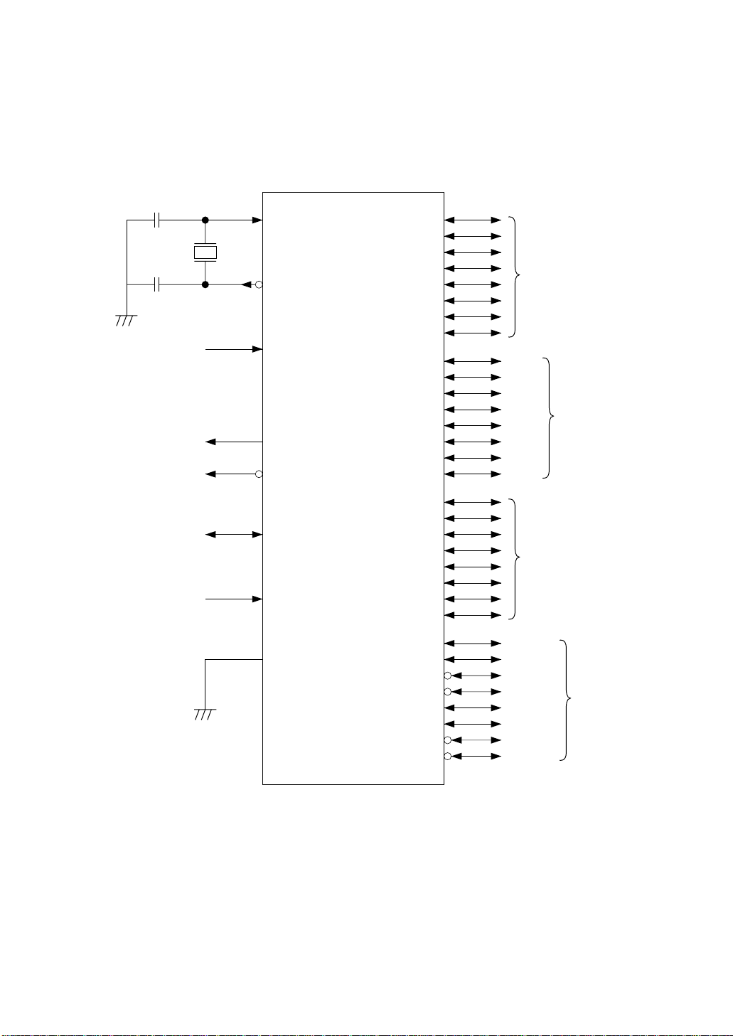
2.1 MSM80C154S/MSM83C154S/MSM85C154HVS Logic Symbols
RESET
ADDRESS LATCH
ENABLE
PROGRAM STORE
ENABLE
CPU MEMORY
SEPARATE
+5(V)
XTAL1
XTAL2
RESET
ALE
PSEN
EA
VCC
P0.0
P0.1
P0.2
P0.3
P0.4
P0.5
P0.6
P0.7
P1.0
P1.1
P1.2
P1.3
P1.4
P1.5
P1.6
P1.7
P2.0
P2.1
P2.2
P2.3
P2.4
P2.5
P2.6
P2.7
PORT 0
(BUS PORT)
T2
T2EX
PORT 1
PORT 2
P3.0
0(V)
Figure 2-1 MSM80C154S/83C154S/85C154HVS logic symbols
VSS
P3.1
P3.2
P3.3
P3.4
P3.5
P3.6
P3.7
RXD
TXD
INT0
INT1
T0
T1/HPDI
WR
RD
11
PORT 3
Page 19
MSM80C154S/83C154S/85C154HVS
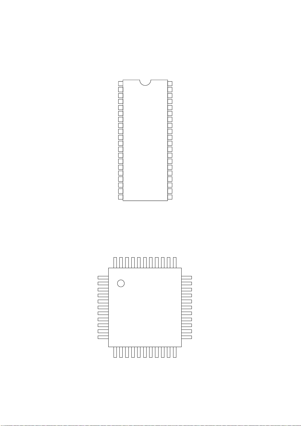
2.2 MSM80C154S/MSM83C154S pin layouts
MSM80C154SRS/MSM83C154SRS
(Top View) 40 Pin Plastic DIP
P3.0/RXD
P3.1/TXD
P3.2/INT0
P3.3/INT1
P3.4/T0
P3.5/T1/HPDI
P3.6/WR
P3.7/RD
XTAL2
XTAL1
VSS
MSM80C154SGS/MSM83C154SGS
(Top View) 44 Pin Plastic Package
10
11
12
13
14
15
16
17
18
19
20
1P1.0/T2
2P1.1/T2EX
3P1.2
4P1.3
5P1.4
6P1.5
7P1.6
8P1.7
9RESET
MSM80C154SRS/MSM83C154SRS
40
39
38
37
36
35
34
33
32
31
30
29
28
27
26
25
24
23
22
21
VCC
P0.0
P0.1
P0.2
P0.3
P0.4
P0.5
P0.6
P0.7
EA
ALE
PSEN
P2.7
P2.6
P2.5
P2.4
P2.3
P2.2
P2.1
P2.0
P1.4
P1.3
P1.2
P1.1/T2EX
P1.0/T2NCVCC
4443424140 39 3837363534
1P1.5
2P1.6
3P1.7
4RESET
5P3.0/RXD
6NC
7P3.1/TXD
8P3.2/INT0
9P3.3/INT1
10P3.4/T0
11P3.5/T1/HPDI
1213141516 17 1819202122
P3.7/RD
P3.6/WR
MSM83C154SGS
VSS
XTAL2
XTAL1
P0.0
O0.1
MSM80C154SGS/
VSS
P2.0
P2.1
P2.2
12
P0.2
33
32
31
30
29
28
27
26
25
24
23
P2.3
P0.3
P0.4
P0.5
P0.6
P0.7
EA
NC
ALE
PSEN
P2.7
P2.6
P2.5
P2.4
Page 20
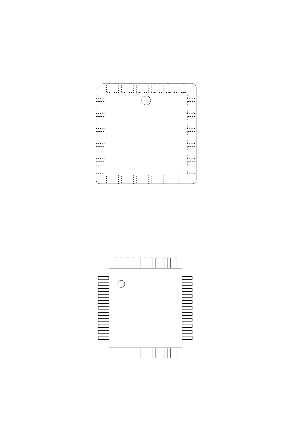
MSM80C154SJS/MSM83C154SJS
(Top View) 44 Pin Plastic QFJ
P1.4
P1.3
P1.2
P1.1/T2EX
P1.0/T2NCVCC
654321
7P1.5
8P1.6
9P1.7
10RESET
11P3.0/RXD
12NC
13P3.1/TXD
14P3.2/INT0
15P3.3/INT1
16P3.4/T0
17P3.5/T1/HPDI
18 19 20 21 22 23 24 25 26 27 28
P3.6/WR
MSM80C154SJS/MSM83C154SJS
VSS
XTAL2
XTAL1
P3.7/RD
P0.0
44 43 42 41 40
NC
P2.0
P2.1
SYSTEM CONFIGURATION
P0.1
P0.2
P0.3
39 P0.4
38 P0.5
37 P0.6
36 P0.7
35 EA
34 NC
33 ALE
32 PSEN
31 P2.7
30 P2.6
29 P2.5
P2.2
P2.3
P2.4
MSM80C154STS/MSM83C154STS
(Top View) 44 Pin Plastic Package
P1.4
P1.3
P1.2
P1.1/T2EX
P1.0/T2NCVCC
4443424140 39 3837363534
1P1.5
2P1.6
3P1.7
4RESET
5P3.0/RXD
6NC
7P3.1/TXD
8P3.2/INT0
9P3.3/INT1
10P3.4/T0
11P3.5/T1/HPDI
1213141516 17 1819202122
P3.7/RD
P3.6/WR
MSM83C154STS
VSS
XTAL2
XTAL1
P0.0
O0.1
P0.2
P0.3
33
P2.1
P2.2
32
31
30
29
28
27
26
25
24
23
P2.3
P2.4
MSM80C154STS/
VSS
P2.0
P0.4
P0.5
P0.6
P0.7
EA
NC
ALE
PSEN
P2.7
P2.6
P2.5
Figure 2-2 MSM80C154S/MSM83C154S pin layout (top view)
13
Page 21

MSM80C154S/83C154S/85C154HVS
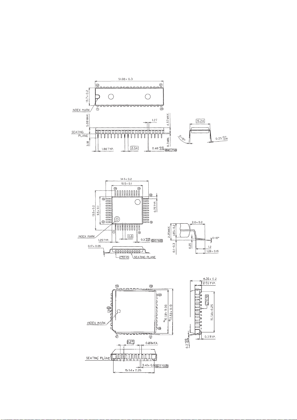
Applicable Packages
40-Pin Plastic DIP (DIP40-P-600-2.54)
44-Pin Plastic QFJ (QFJ44-P-S650-1.27)
44-Pin Plastic QFP (DFP44-P-910-0.80-2K)
44-Pin Plastic TQFP (TQFP44-P-1010-0.80-K)
40-Pin Ceramic Piggy Back (ADIP40-C-600-2.54)
MSM80C154S RS
MSM83C154S-XXX RS
MSM80C154S JS
MSM83C154S-XXX JS
MSM80C154S GS-2K
MSM83C154S-XXX GS-2K
MSM80C154S TS-K
MSM83C154S-XXX TS-K
MSM85C154HVS
14
Page 22
SYSTEM CONFIGURATION
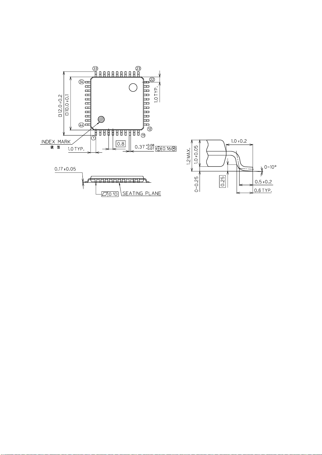
2.2.1 MSM80C154S/MSM83C154S external dimensions
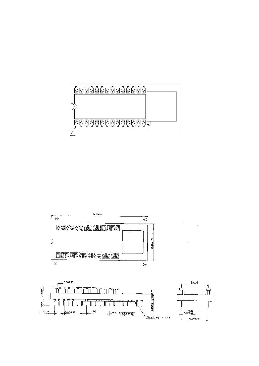
MSM80C154SRS/MSM83C154SRS
40-pin Plastic DIP (DIP40-P-600-2.54)
MSM80C154SGS/MSM83C154SGS
44-Pin Plastic QFP (QFP44-P-910-0.80-2K)
MSM80C154SJS/MSM83C154SJS
44-Pin Plastic QFJ (QFJ44-P-S650-1.27)
Figure 2-3 MSM80C154S/MSM83C154S external dimensions
15
Page 23
MSM80C154S/83C154S/85C154HVS
MSM80C154STS/MSM83C154STS
44-Pin Plastic TQFP (TQFP44-P-1010-0.80-K)
16
Page 24
SYSTEM CONFIGURATION
2.2.2 MSM85C154HVS pin layout and external dimensions
M85C154H
2764/27128
Pin 1 for 2764, 27128
* The MSM85C154HVS pin layout of bottom side is the same as the pin layout for
MSM83C154SRS.
OKI
JAPAN XXXX
* The 27C64/128 device should be used for EPROM.
40-Pin Ceramic Piggy Back (ADIP40-C-600-2.54)
Figure 2-4 MSM85C154HVS pin layout and external dimensions
17
Page 25
MSM80C154S/83C154S/85C154HVS
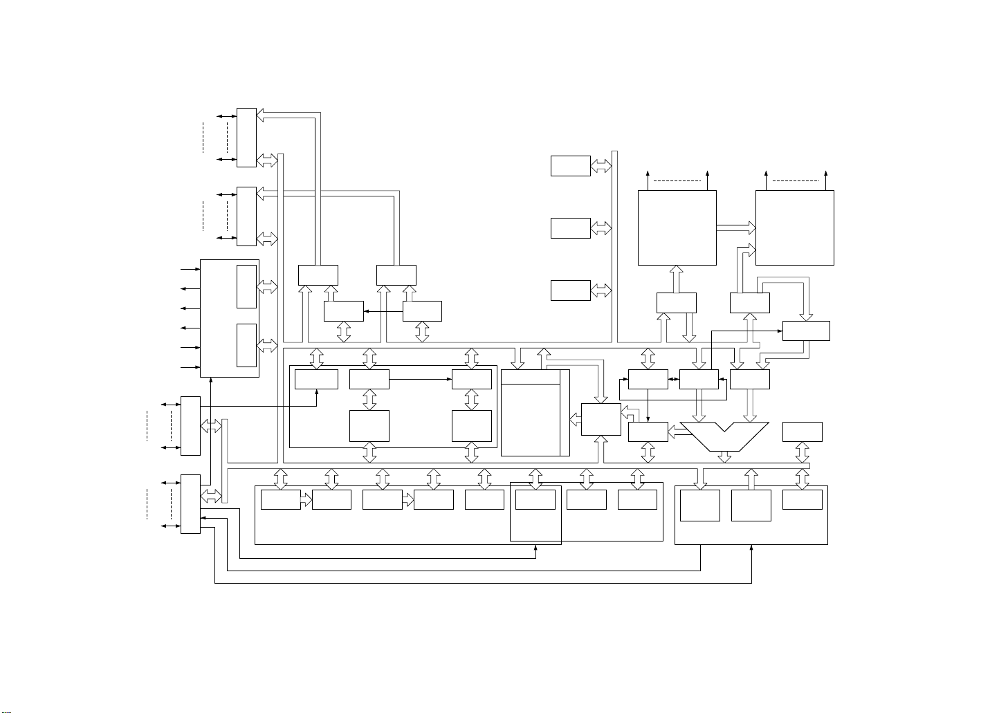
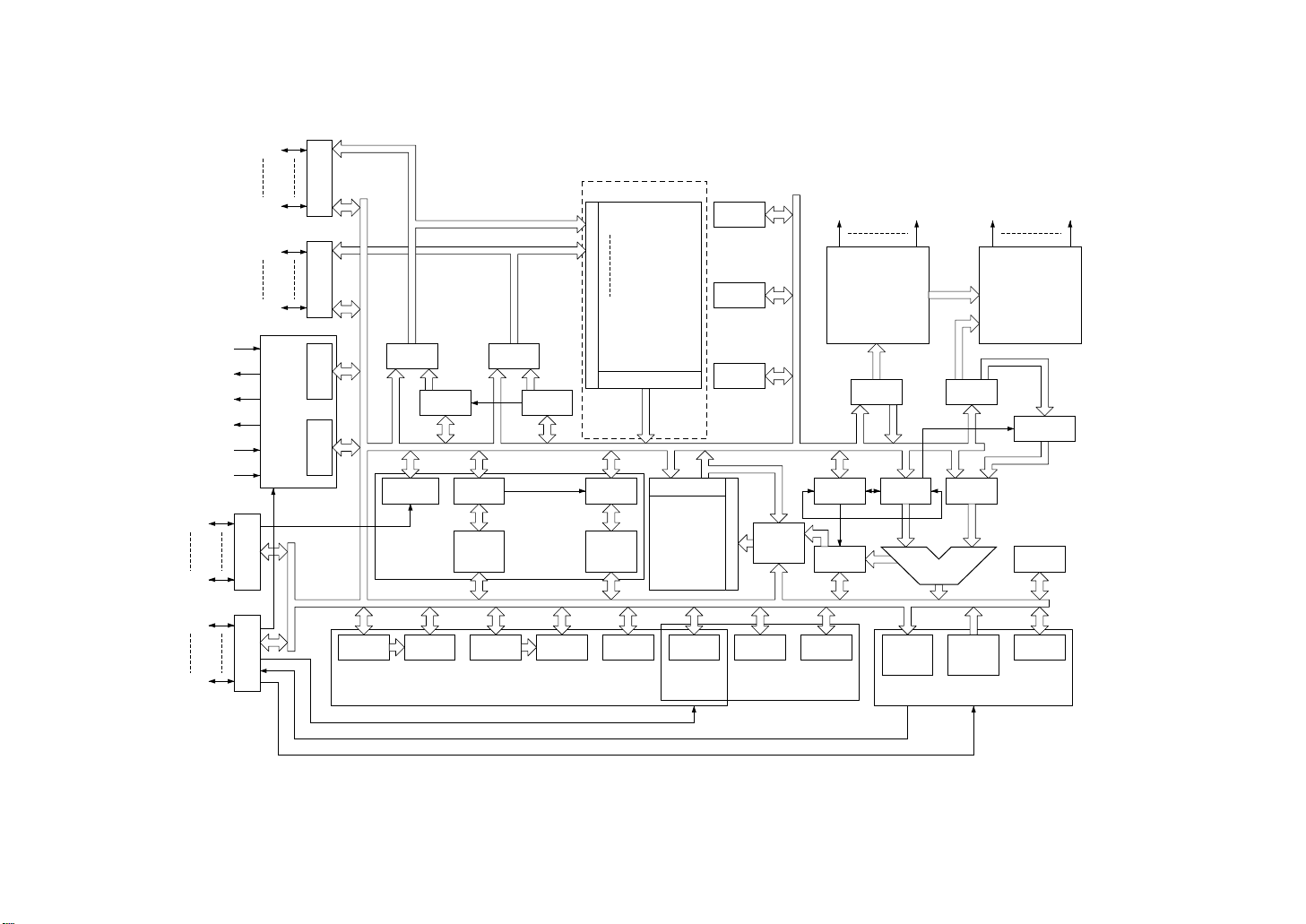
2.3 MSM80C154S Block Diagram
18
P2.0
PORT 2
P2.7
P0.0
PORT 0
Figure 2-5 MSM80C154S block diagram
P0.7
OSC AND TIMING
XTAL1
PCON IOCON
PCHL PCLL
XTAL2
ALE
PSEN
EA
RESET
T2CON TL2
P1.0
PORT 1
P1.7
P3.0
PORT 3
TH1
P3.7
DPH
CONTROL SIGNAL SIGNALR/W
SPECIAL
FUNCTION
DPL
PLA
REGISTER
ADDRESS
DECODER
SP
PCH
PCL
IR AIR
C-ROM
2H
R/W AMP
256WORD
×8bit
ACC TR2 TR1
RAMDP
PSW
INTERRUPT
SBUF
(T)
ALU
SBUF
(R)
SERIAL IO
BR
TH2
TIMER/
COUNTER 2
RCAP
RCAP
2L
TL1 TH0 TL0 TMOD TCON IE IP SCON
TIMER/COUNTER 0&1
Page 26
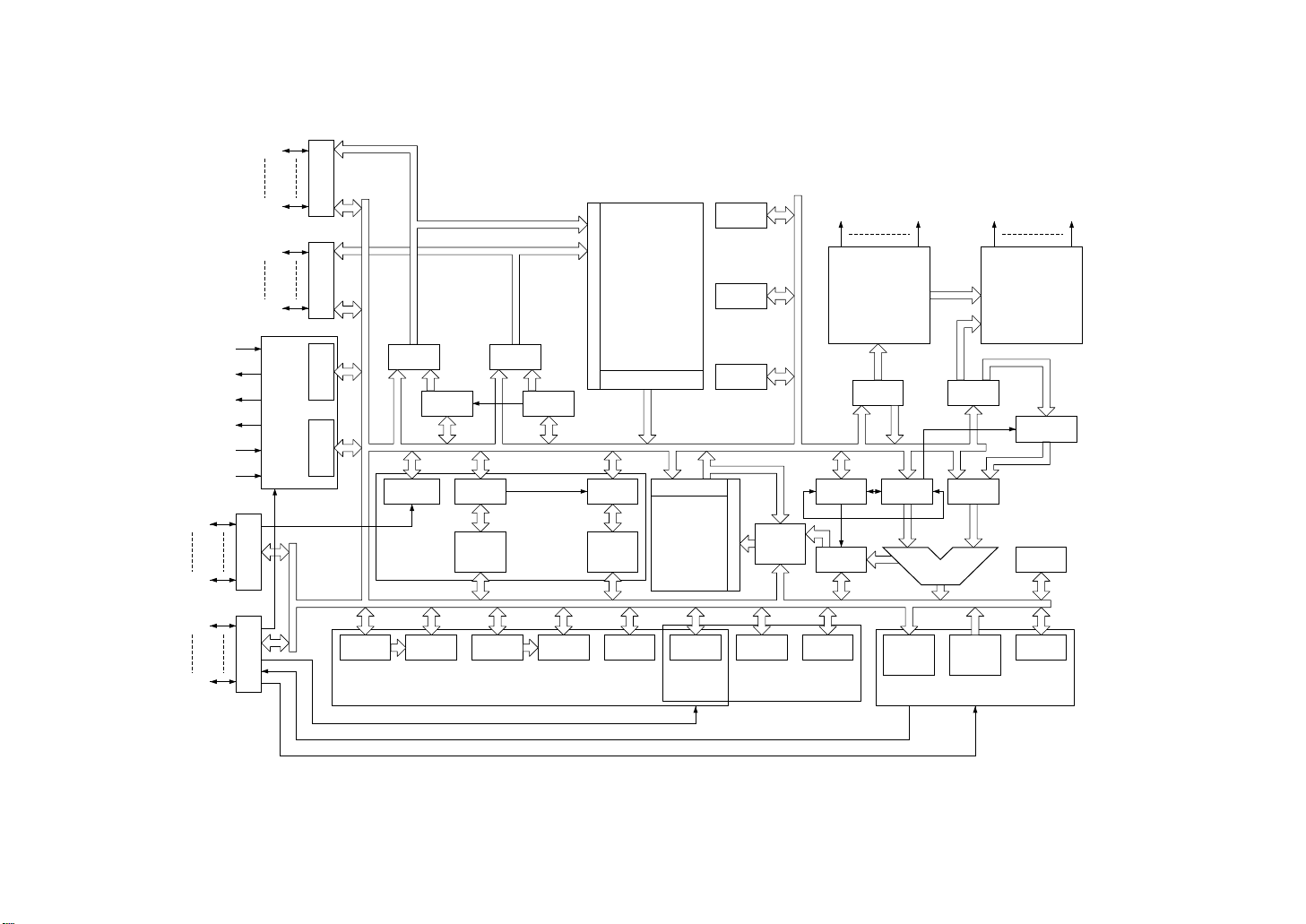
2.4 MSM83C154S Block Diagram
19
P2.0
PORT 2 PORT 0 PCON IOCON
P2.7
P0.0
Figure 2-6 MSM83C154S block diagram
P0.7
XTAL1
OSC AND TIMING
PCHL PCLL
XTAL2
ALE
PSEN
EA
RESET
T2CON TL2
P1.0
PORT 1 PORT 3
P1.7
P3.0
TH1
P3.7
DPH
CONTROL SIGNAL SIGNALR/W
SPECIAL
ROM
16KWORD
×8bit
DPL
PLA
FUNCTION
REGISTER
ADDRESS
DECODER
SP
IR AIR
PCH
SENSE AMP
PCL
C-ROM
2H
R/W AMP
256WORD
×8bit
ACC TR2 TR1
RAMDP
PSW
INTERRUPT
SBUF
(T)
ALU
SBUF
(R)
SERIAL IO
BR
TH2
TIMER/
COUNTER 2
RCAP
RCAP
2L
TL1 TH0 TL0 TMOD TCON IE IP SCON
TIMER/COUNTER 0&1
SYSTEM CONFIGURATION
Page 27
MSM80C154S/83C154S/85C154HVS
2.5 MSM85C154HVS Block Diagram
20
P2.0
PORT 2 PORT 0 PCON IOCON
P2.7
P0.0
Figure 2-7 MSM85C154HVS block diagram
P0.7
XTAL1
OSC AND TIMING
PCHL PCLL
XTAL2
ALE
PSEN
EA
RESET
T2CON TL2
P1.0
PORT 1 PORT 3
P1.7
P3.0
TH1
TL1 TH0 TL0 TMOD TCON IE IP SCON
P3.7
PCH
PCL
TIMER/
COUNTER 2
RCAP
2L
TIMER/COUNTER 0&1
SOCKET
A0
EXTERNAL
A13
16KWORD
×8bit
D0 ... D7
TH2
RCAP
2H
ROM
R/W AMP
256WORD
×8bit
DPH
DPL
SP
RAMDP
INTERRUPT
CONTROL SIGNAL SIGNALR/W
SPECIAL
FUNCTION
PLA
REGISTER
ADDRESS
DECODER
IR AIR
ACC TR2 TR1
PSW
SBUF
(T)
ALU
SBUF
(R)
SERIAL IO
C-ROM
BR
Page 28
SYSTEM CONFIGURATION
2.6 Timing and Control
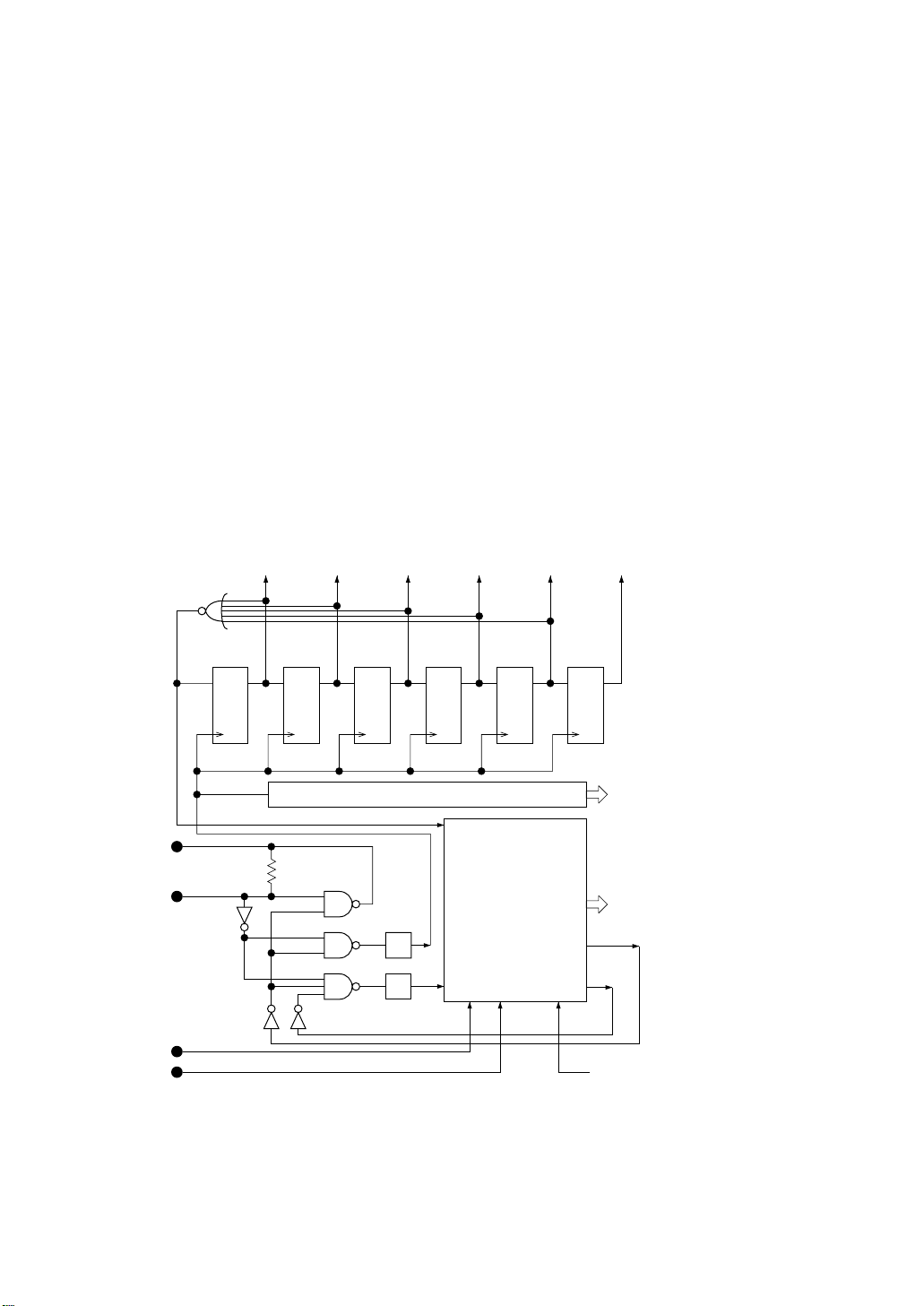
2.6.1 Outline of MSM80C154S/MSM83C154S timing
The MSM80C154S/MSM83C154S devices are both equipped with a built-in oscillation
inverter (see Figure 2-8) for use in the generation of clock pulses by external crystal or ceramic
resonator. These clock pulses are passed to the timing counter and control circuits where the
basic timing and control signals required for internal control purposes are generated.
The basic timing consists of state 1 (S1) thru state 6 (S6) (see Figure 2-9) where each state
cycle is based on two XTAL1·2 fundamental clock pulses. The interval from S1 thru S6 forms
a single machine cycle with a total of 12 fundamental clock pulses. 1-byte 1-machine cycle
and 2-byte 1-machine cycle instructions are fetched into the instruction register during
M1·S1, decoded during M1·S2, and executed during M1·S3 thru M1·S6. The second byte is
fetched during M1·S4. 1-byte 2-machine cycle, 2-byte 2-machine cycle, and 3-byte 2machine cycle instructions are also fetched during M1·S1, decoded during M1·S2, and
executed during M1·S3 thru M2·S6. The second and third bytes are fetched during M1·S4,
M2·S1, or M2·S4. The number of clocks used is 24. 1-byte 4-machine cycle instructions are
involved in multiplication and division operations where 48 clocks are used.
S1 S2 S3 S4 S5 S6
XTAL2
XTAL1
RESET
INT
DQ
Figure 2-8 Oscillator, timing counter, and control stage block diagram
DQ DQ DQ DQ DQ
S I/O & TIMER CONTROL
CPU CONTROL
1/2
1/2
POWER DOWN
IDLE
S I/O
TIMER & INTERRUPT
CPU
PLA
PLA OUT
21
Page 29
MSM80C154S/83C154S/85C154HVS
M1
Instruction excecution
TM+1
M2
M1
M1
S1 S2 S3 S4 S5 S6
S1 S2 S3 S4 S5 S6
S1 S2 S3 S4 S5 S6
DPL & Rr
PCL PCL PCL PCL PCL PCLACC & RAM
PORT NEW DATA
DATA STABLE DATA STABLE
PORT OLD DATA
Instruction decoding
Instruction decoding
PC+1 PC+1
Instruction excecution
PC+1
Instruction excecution
TM+1 TM+1
TM+1
CYCLE
S1 S2 S3 S4 S5 S6
STEP
1
XTAL1
PCH PCH PCH PCH DPH & PORT DATA PCH PCH PCH
0
1
0
1
0
1
0
1
0
1
0
1
0
ALE
PSEN
RD/WR
PORT–0
PORT–2
CPU←PORT
Instruction decoding
1
0
PORT←CPU
Figure 2-9 MSM80C154S/MSM83C154S fundamental timing
22
PC+1 PC+1
Page 30

SYSTEM CONFIGURATION
2.6.2 Major synchronizing signals
(1) ALE (Address Latch Enable)
The ALE signal is used as a clock signal where the address signals 0 thru 7 output from
CPU port 0 can be latched externally when external program or external data memory
(RAM) is used.
Although two ALE signal outputs are obtained in a single machine cycle during normal
operations, no output is obtained during output of the RD/WR signal when an external
memory instruction (MOVX...... ) is executed.
(2) PSEN (Program Store Enable)
The PSEN output signal is generated during execution of an external program. The
output is obtained when an instruction or data is fetched.
The PSEN signal is valid when at “0” level, and external program data is enabled when
in this valid state.
Although two PSEN signal outputs are obtained in a single machine cycle during
normal operations, no output is obtained during output of the RD/WR signal when an
external data memory instruction (MOVX...... ) is executed.
(3) WR (Write Strobe)
The WR output signal is obtained when an external data memory instruction (MOVX
@Rr, A or MOVX @ DPTR, A) is executed.
CPU port 0 output data is written in the external RAM when the WR signal is at “0” level.
(4) RD (Read Strobe)
The RD output signal is obtained when an external data memory instruction (MOVX
A, @ Rr or MOVX A, @ DPTR) is executed.
The external RAM is enabled and output data is passed to CPU port 0 when the RD
signal is at “0” level.
23
Page 31

MSM80C154S/83C154S/85C154HVS
2.6.3 MSM80C154S fundamental operation time charts
(1) External program memory read cycle timing chart
M1 or M2
XTAL1
ALE
PSEN
PORT–0
PORT–2
1
0
1
0
1
0
1
0
1
PCH OUT
0
Figure 2-10 MSM80C154S external program memory read cycle timing chart
(2) MOVX A, @Rr
S1 S2 S3 S4 S5 S6M1S1 S2 S3 S4 S5 S6
INST IN
PCL
OUT
INST IN
PCL
OUT
PCH OUT PCH OUT PCH OUT
INST IN
PCL
INST IN INST IN
OUT
PCL
OUT
S1
PCH OUT
XTAL1
ALE
PSEN
RD
PORT–0
PORT–2
S1 S2 S3 S4 S5 S6M1S1 S2 S3 S4 S5 S6M2S1
1
0
1
0
1
0
1
0
INST IN
1
0
1
PCH OUT
0
PCL
OUT
PCH OUT PORT 2 LATCH DATA OUT
Figure 2-11 MSM80C154S MOVX A, @Rr execution
Rr
OUT
RAM DATA IN
EXT RAM
DATA
PCL
OUT
24
INST IN
PCH OUT
Page 32

(3) MOVX @Rr, A
SYSTEM CONFIGURATION
S1 S2 S3 S4 S5 S6M1S1 S2 S3 S4 S5 S6M2S1
XTAL1
ALE
PSEN
WR
PORT–0
PORT–2
1
0
1
0
1
0
1
0
INST IN
1
0
1
PCH OUT
0
Figure 2-12 MSM80C154S MOVX @Rr, A execution
(4) MOVX A, @DPTR
S1 S2 S3 S4 S5 S6M1S1 S2 S3 S4 S5 S6M2S1
PCL
OUT
PCH OUT PORT 2 LATCH DATA OUT
Rr
OUT
ACC DATA OUT
PCL
INST IN
OUT
PCH OUT
XTAL1
ALE
PSEN
RD
PORT–0
PORT–2
1
0
1
0
1
0
1
0
INST IN
1
0
1
PCH OUT
0
Figure 2-13 MSM80C154S MOVX A, @DPTR execution
PCL
OUT
PCH OUT DPH OUT
DPL
OUT
RAM DATA IN
EXT RAM
DATA
25
PCL
INST IN
OUT
PCH OUT
Page 33

MSM80C154S/83C154S/85C154HVS
(5) MOVX @DPTR, A
S1 S2 S3 S4 S5 S6M1S1 S2 S3 S4 S5 S6M2S1
XTAL1
ALE
PSEN
WR
PORT–0
PORT–2
1
0
1
0
1
0
1
0
INST IN
1
0
1
PCH OUT
0
Figure 2-14 MSM80C154S MOVX @DPTR, A execution
PCL
OUT
PCH OUT DPH OUT
DPL
OUT
(6) MOV direct, PORT [0, 1, 2, 3] execution
S1 S2 S3 S4 S5 S6M1S1 S2 S3 S4 S5 S6M2S1
ACC DATA OUT
PCL
INST IN
OUT
PCH OUT
XTAL1
ALE
PSEN
PORT 0,1,2,3
PIN DATA
CPU DATA
SAMPLED
1
0
1
0
1
0
1
0
1
0
Figure 2-15 MSM80C154S MOV direct, PORT[0, 1, 2, 3] execution
PIN DATA STABLE
26
Page 34

2.6.4 MSM83C154S fundamental operation time charts
(1) MOVX A, @Rr
S1 S2 S3 S4 S5 S6M1S1 S2 S3 S4 S5 S6M2S1
SYSTEM CONFIGURATION
XTAL1
ALE
PSEN
RD
PORT–0
PORT–2
1
0
1
0
1
0
1
0
1
0
1
0
(2) MOVX @Rr, A
RAM DATA IN
PORT 0 LATCH DATA
Figure 2-16 MSM83C154S MOVX A, @Rr execution
S1 S2 S3 S4 S5 S6M1S1 S2 S3 S4 S5 S6M2S1
Rr
OUT
PORT 2 LATCH DATA OUT
EXT RAM
DATA
FLOATING
XTAL1
ALE
PSEN
WR
PORT–0
PORT–2
1
0
1
0
1
0
1
0
1
PORT 0 LATCH DATA
0
1
0
Figure 2-17 MSM83C154S MOVX @Rr, A execution
Rr
OUT
PORT 2 LATCH DATA OUT
ACC DATA OUT
27
FLOATING
Page 35

MSM80C154S/83C154S/85C154HVS
(3) MOVX A, @DPTR
S1 S2 S3 S4 S5 S6M1S1 S2 S3 S4 S5 S6M2S1
XTAL1
ALE
PSEN
RD
PORT–0
PORT–2
1
0
1
0
1
0
1
0
1
PORT 0 LATCH DATA
0
1
PORT 2 LATCH DATA OUT
0
Figure 2-18 MSM83C154S MOVX A, @DPTR execution
(4) MOVX @DPTR, A
S1 S2 S3 S4 S5 S6M1S1 S2 S3 S4 S5 S6
DPL
OUT
RAM DATA IN
EXT RAM
DATA
DPH OUT
FLOATING
PORT 2 LATCH
DATA OUT
M2
S1
XTAL1
ALE
PSEN
WR
PORT–0
PORT–2
1
0
1
0
1
0
1
0
1
PORT 0 LATCH DATA
0
1
PORT 2 LATCH DATA OUT
0
Figure 2-19 MSM83C154S MOVX @DPTR, A execution
DPL
OUT
ACC DATA OUT
DPH OUT
28
FLOATING
PORT 2 LATCH
DATA OUT
Page 36

(5) MOV direct, PORT [0, 1, 2, 3] execution
S1 S2 S3 S4 S5 S6M1S1 S2 S3 S4 S5 S6M2S1
SYSTEM CONFIGURATION
XTAL1
ALE
PSEN
PORT 0,1,2,3
PIN DATA
CPU DATA
SAMPLED
1
0
1
0
1
0
1
0
1
0
Figure 2-20 MSM83C154S MOV direct, PORT[0, 1, 2, 3] execution
PIN DATA STABLE
29
Page 37

MSM80C154S/83C154S/85C154HVS
2.7 Instruction Register (IR) and Instruction Decoder (PLA)
MSM80C154S/MSM83C154S operations are based on an instruction code address method.
Hence, in addition to the instruction code instruction register (IR) and instruction decoder
(PLA), these devices also include an instruction register (AIR) and register manipulation
decoder (PLA) for data addresses and bit addresses.
Operation codes are passed to the IR, and data and bit addresses are passed to the AIR. CPU
control signals are formed at the respective PLA for each instruction register, thereby
activating the CPU. The block diagram is outlined in Figure 2-21.
Timing
AND
Matrix
AIR
Control signals
Data bus
WAIR
Data bus
WIR
IR
Decoder
Matrix
Decoder
PLA
Timing
AND
Control signals
PLA
Figure 2-21 lR and PLA block diagram
30
Page 38

SYSTEM CONFIGURATION
2.8 Arithmetic Operation Section
(1) Outline
The MSM80C154S/MSM83C154S arithmetic operation section consists of
(1) an arithmetic operation instruction decoder, and
(2) an arithmetic and logic unit [ALU].
(2) Arithmetic operation instruction decoder:
Arithmetic operation instructions are passed to the instruction register (IR) and then to
the PLA where they are converted into control signals.
The control signals from the PLA are used to control ALU peripheral circuits and ALU
arithmetic operations (ADD, AND, OR, EOR).
(3) Arithmetic and logic unit [ALU]:
Upon reception of 8-bit data from one or two data sources the ALU processes that data
in accordance with control signals from the PLA. The ALU is capable of executing the
following processes:
• Additions and subtractions with and without carry
• Increments (+1) and decrements (–1)
• Bit complements
• Rotations (either direction with and without carry)
• BCD (decimal adjust)
• Carry, auxiliary carry, and overflow signal output
• Multiplications and divisions
• Bit detection
• Exchange of low and high order nibbles
• Logical AND, logical OR, and exclusive OR
If a bit-3 auxiliary carry (AC), a bit-7 carry (CY), or an overflow (OV) is generated as a
result of the arithmetic operation executed by the ALU, that result is set in the program
status word (PSW 0D0H).
PSW(0D0H)
CY
7AC6F05
Figure 2-22 Program status word
RS14RS03OV2F11P
31
0
Page 39

MSM80C154S/83C154S/85C154HVS
2.9 Program Counter
The MSM80C154S/MSM83C154S program counter has a 16-bit configuration PC0 thru
PC15, as shown in Figure 2-23.
ENABLE ROM
MSM83C154S INTERNAL ROM
16KWORD × 8BIT
CPU INTERNAL
DATA BUS
EXTERNAL
ROM MODE
Q8Q9Q10Q11Q12Q13Q14Q15
D8D9D10D11D12D13D14D15
CPU INTERNAL DATA BUS
Figure 2-23 MSM80C154S/MSM83C154S program ounter
Q0Q1Q2Q3Q4Q5Q6Q7
PC+1
D0D1D2D3D4D5D6D7
This program counter is a binary up-counter which is incremented by 1 each time one byte
of instruction code is fetched. When the program counter is counted by 1 after counter
contents have reached 0FFFFH, the counter is returned to 0000H. MSM83C154S is
automatically switched to external ROM mode when the counter contents exceed 3FFFH.
32
Page 40

SYSTEM CONFIGURATION
2.10 Program Memory and External Data Memory
2.10.1 MSM80C154S/MSM83C154S program area and external ROM connections
Since MSM80C154S/MSM83C154S are equipped with a 16-bit program counter, these
devices can execute programs of up to 64K bytes (including both internal and external
programs).
Since the MSM80C154S is not equipped with an internal program ROM, however, only
external instructions are executed. MSM83C154S, on the other hand, is equipped with a 16K
byte program ROM which enables it to execute internal instructions from address 0 thru
address 16383. External instructions are executed when the address is greater than 16383.
The program area is outlined in Figure 2-24, and a diagram of ROM connections made when
external instructions are executed is shown in Figure 2-25.
0FFFFH65535
4000H16384
3FFFH16383
MSM80C154S external ROM area
002CH44
002BH43
Timer interrupt 2 start address 43 002BH
Serial I/O interrupt start address 35 0023H
Timer interrupt 1 start address 27 001BH
External interrupt 1 start address 19 0013H
Timer interrupt 0 start address 11 000BH
External interrupt 0 start address 3 0003H
2 0002H
MSM83C154S internal ROM area MSM83C154S external ROM area
0
Figure 2-24 MSM80C154S/MSM83C154S program area
1 0001H
CPU reset start address 0 0000H76543210
33
Page 41

Figure 2-25 MSM80C154S/MSM83C154S external ROM connection diagram
MSM80C154S/83C154S/85C154HVS
34
P0.0
P0.1
P0.2
P0.3
P0.4
MSM80C154S/MSM83C154S
P0.5
P0.6
P0.7
ALE
P2.0
P2.1
P2.2
P2.3
P2.4
P2.5
P2.6
P2.7
PSEN
D0
D1
MSM74HC373
D2
D3
D4
D5
D6
D7
LATCH
Q0
Q1
Q2
Q3
Q4
Q5
Q6
Q7
A0
A1
A2
A3
A4
A5
A6
A7
A8
A9
A10
A11
A12
A13
A14
A15
CS
OUTPUT ENABLE
ROM
64kW × 8BIT
Q7Q6Q5Q4Q3Q2Q1Q0
Page 42

SYSTEM CONFIGURATION
2.10.2 Procedures and circuit connections used when external data memory (RAM)
is accessed by data pointer (DPTR)
The MSM80C154S/MSM83C154S can be connected to an external 64K word × 8-bit data
memory (RAM) when accessing the memory by data pointer (DPTR).
The data pointer (DPTR) consists of DPL and DPH registers. The DPL register contents serve
as addresses 0 thru 7 of the external data memory, and the DPH register contents serve as
addresses 8 thru 15.
The MOVX @DPTR, A instruction is used when accumulator contents are transferred to an
external data memory, and the MOVX A, @DPTR instruction is used when external data
memory contents are transferred to the accumulator. The external data memory connection
diagram is shown in Figure 2-26 and the external data memory access time chart is shown
in Figure 2-27.
When the data pointer indirect external memory instruction is executed, the CPU passes the
DPL register contents to port 0, and the port 0 contents are latched externally by ALE signal.
Data stored in the latch serves as the lower order addresses 0 thru 7 of the external data
memory (RAM), and the DPH register contents passed to port 2 serve as the higher order
addresses 8 thru 15 for addressing of the external data memory.
The WR or RD external data memory control signal is subsequently generated by the CPU
to enable transfer of data between port 0 and the external data memory.
35
Page 43

Figure 2-26 Connection circuit for external data memory addressed by DPTR
MSM80C154S/83C154S/85C154HVS
36
P0.0
P0.1
P0.2
P0.3
P0.4
MSM80C154S/MSM83C154S
P0.5
P0.6
P0.7
ALE
P2.0
P2.1
P2.2
P2.3
P2.4
P2.5
P2.6
P2.7
WR
D0
D1
MSM74HC373
D2
D3
D4
D5
D6
D7
LATCH
Q0
Q1
Q2
Q3
Q4
Q5
Q6
Q7
A0
A1
A2
A3
A4
A5
A6
A7
A8
A9
A10
A11
A12
A13
A14
A15
R/W
I/O
76543210
ROM
64kW × 8BIT
RD
CS
Page 44

SYSTEM CONFIGURATION
M1
M2
M1
S1 S2 S3 S4 S5 S6
S1 S2 S3 S4 S5 S6
S1 S2 S3 S4 S5 S6
M1
S1 S2 S3 S4 S5 S6
M2
S1 S2 S3 S4 S5 S6
MOVX @DPTR, A
M1
S1 S2 S3 S4 S5 S6
RAM DATA IN
MOVX A, @DPTR
M1
S1 S2 S3 S4 S5 S6
S6
M1
PCL PCL PCL PCL PCL PCLACC DATADPL
1
XTAL1
INSTRUCTION IN
PCH PCH PCH PCH DPH PCH PCH PCH
0
1
0
ALE
1
PSEN
0
PCL
1
0
PORT–0
1
0
PORT–2
1
0
WR
S1 S2 S3 S4 S5 S6
S6
1
XTAL1
0
1
ALE
Figure 2-27 DPTR external data memory access timing
37
0
1
PSEN
PCL PCL PCL PCL PCL PCLDPL
INSTRUCTION IN
PCH PCH PCH PCH DPH PCH PCH PCH
PCL
0
1
0
1
PORT–0
PORT–2
1
0
0
RD
Page 45

MSM80C154S/83C154S/85C154HVS
2.10.3 Procedures and circuit connections used when external data memory (RAM)
is accessed by registers R0 and R1
The MSM80C154S/MSM83C154S can be connected to an external 256 word ¥ 8-bit data
memory (RAM) when addressing the memory according to the contents of registers R0 and
R1 in the internal data memory (RAM).
The MOVX @Rr, A instruction is used when accumulator contents are transferred to an
external data memory, and the MOVX A, @Rr instruction is used when external data memory
contents are transferred to the accumulator. The external data memory connection diagram
is shown in Figure 2-28 and the external data memory access time chart is shown in Figure
2-29.
When the indirect register external memory instruction is executed, the CPU passes the R0
or R1 register contents to port 0, and the port 0 contents are latched externally by the ALE
signal. Data stored in the latch serves as the addresses 0 thru 7 of the external data memory.
The WR or RD external data memory control signal is subsequently generated by the CPU
to enable transfer of data between port 0 and the external data memory.
However, if the port 2 latched data is used in addresses 8 thru 15 of the external data memory,
the circuit connections are the same as when the data pointer (DPTR) is used, thereby
enabling a 64K byte ¥ 8-bit data memory to be accessed.
38
Page 46

76543210
I/O
A0A1A2A3A4A5A6
ROM
256W × 8BIT
A7
SYSTEM CONFIGURATION
CS
R/W
Q0Q1Q2Q3Q4Q5Q6
MSM74HC373
D0D1D2D3D4D5D6
P0.0
P0.1
P0.2
P0.3
P0.4
P0.5
P0.6
Q7
D7
P0.7
LATCH
ALE
WR
RD
MSM80C154S/MSM83C154S
Figure 2-28 Connection circuit for external data memory addressed by register R0 or R1
39
Page 47

MSM80C154S/83C154S/85C154HVS
M1
M2
M1
S1 S2 S3 S4 S5 S6
S1 S2 S3 S4 S5 S6
S1 S2 S3 S4 S5 S6
M1
S1 S2 S3 S4 S5 S6
M2
S1 S2 S3 S4 S5 S6
MOVX @Rr, A
M1
S1 S2 S3 S4 S5 S6
RAM DATA IN
MOVX A, @Rr
M1
S1 S2 S3 S4 S5 S6
S6
1
XTAL1
PCL PCL PCL PCL PCL PCLACC DATARr
INSTRUCTION IN
PCH PCH PCH PCH PORT 2 LATCH DATA PCH PCH PCH
0
1
0
ALE
1
0
PSEN
PCL
1
0
PORT–0
1
0
PORT–2
1
WR
M1
S1 S2 S3 S4 S5 S6
S6
0
1
XTAL1
0
1
0
ALE
Figure 2-29 Register R0/R1 external data memory access timing
40
PCL PCL PCL PCL PCL PCLRr
INSTRUCTION IN
PCL
1
0
1
PSEN
PORT–0
0
PCH PCH PCH PCH PORT 2 LATCH DATA PCH PCH PCH
1
0
PORT–2
1
0
RD
Page 48

3. CONTROL
Page 49

MSM80C154S/83C154S/85C154HVS
42
Page 50

CONTROL
3. CONTROL
3.1 Oscillators: XTAL1
XTAL2
An oscillator is formed by connecting a crystal or ceramic resonator between the XTAL1 and
XTAL2 pins of the MSM80C154S/MSM83C154S devices.
If an external clock is applied to XTAL1, the input should be at 50% duty and C-MOS level.
IDLE MODE
PD & HPD MODE
C
*
XTAL
C
*
XTAL1
1MΩ
XTAL2
MSM80C154S/MSM83C154S
CPU CONTROL CLOCK
TIMER, S I/O & INTERRUPT
* The capacity of the compensating capacitor depends on the crystal resonator.
* The XTAL1·2 frequency depends on VCC.
Figure 3-1 Crystal resonator connection diagram
43
Page 51

MSM80C154S/83C154S/85C154HVS
IDLE MODE
PD & HPD MODE
C
*
C
*
XTAL1
1MΩ
XTAL2
MSM80C154S/MSM83C154S
CPU CONTROL CLOCK
TIMER, S I/O & INTERRUPT
* The capacity of the compensating capacitor depends on the ceramic resonator.
* The XTAL1·2 frequency depends on VCC.
Figure 3-2 Ceramic resonator connection diagram
IDLE MODE
CPU CONTROL CLOCK
PD & HPD MODE
XTAL1
74HC04
*CLOCK
XTAL2
MSM80C154S/MSM83C154S
* Supply of 50% duty clock
Figure 3-3 External clock supply circuit
TIMER, S I/O & INTERRUPT
1MΩ
44
Page 52

CONTROL
3.2 CPU Resetting
3.2.1 Outline
If a reset signal (kept at “1” level for at least 1µsec) is applied to the RESET pin when the
correct voltage (in respect to the various specifications) is applied to the MSM80C154S/
MSM83C154S VCC pin, a reset signal is stored in the CPU even if the XTAL1·2 oscillators
have been stopped.
The internally stored reset signal is used in direct initialization (setting to “1”) of ports 0, 1, 2,
and 3. All of the special function registers are then initialized (set to “0”) two machine cycles
after the XTAL1·2 oscillator commences regular operation.
When the reset is released, instruction execution is started in the third machine cycle if the
reset signal is changed from “1” level to “0” level before the M1·S1 signal leading edge, and
in the fifth machine cycle if the reset signal is changed from “1” to “0” after the leading edge.
The reset circuit block diagram is shown in Figure 3-4, the reset start time charts in Figures
3-5 and 3-6, and the reset release time charts in Figures 3-7 and 3-8.
CC
V
+
–
RESET
•
R=40KΩ
•
CPU RESET CONTROLIN
Figure 3-4 MSM80C154S/MSM83C154S reset circuit block diagram
45
Page 53

MSM80C154S/83C154S/85C154HVS
M1
S1 S2 S3 S4 S5 S6
M2
S1 S2 S3 S4 S5 S6
M1
M1 or M2
S1 S2 S3 S4 S5 S6
S1 S2 S3 S4 S5 S6
S6
1
XTAL1
CPU RESET EXCECUTE CYCLE
FLOATING
PORT DATA = 1
PORT DATA = 1
PORT DATA = 1
PORT DATA
PORT DATA
PORT DATA
PORT DATA
0
1
0
1
0
1
0
1
0
1
0
1
0
1
0
1
0
1
0
ALE
PSEN
PORT 0
PORT 1
PORT 2
PORT 3
RESET
CPU RESET
CONTROL
RESET
EXCECUTE
Figure 3-5 Reset execution time chart (internal ROM mode)
46
Page 54

M1
M2
CONTROL
S1 S2 S3 S4 S5 S6
S1 S2 S3 S4 S5 S6
M1
M1 or M2
S1 S2 S3 S4 S5 S6
S1 S2 S3 S4 S5 S6
S6
1
XTAL1
CPU RESET EXCECUTE CYCLE
FLOATING
PORT DATA = 1
PCL
PCH PCH
0
1
0
1
0
1
0
1
0
1
0
1
0
ALE
PSEN
PORT 0
PORT 2
RESET
CPU RESET
CONTROL
1
0
RESET
EXCECUTE
PORT DATA = 1
PORT DATA = 1
PORT DATA
PORT DATA
1
0
1
0
PORT 1
PORT 3
Figure 3-6 Reset execution time chart (external ROM mode)
47
Page 55

MSM80C154S/83C154S/85C154HVS
M1
M2
M1
M1
S1 S2 S3 S4 S5 S6
S1 S2 S3 S4 S5 S6
FLOATING
PORT DATA = 1
PORT DATA = 1
EXCECUTE CYCLE
PORT DATA = 1
CPU RESET EXCECUTE CYCLE
S1 S2 S3 S4 S5 S6 S1 S2 S3 S4 S5 S6
S6
1
0
1
0
1
0
1
0
1
0
1
0
1
0
1
0
1
0
1
0
XTAL1
ALE
PSEN
PORT 0
PORT 1
PORT 2
PORT 3
RESET
CPU RESET
CONTROL
RESET
EXCECUTE
Figure 3-7 Reset release time chart (internal ROM mode)
48
Page 56

M1
CONTROL
PCLPCLPCL
M2
M1
M1
S1 S2 S3 S4 S5 S6
S1 S2 S3 S4 S5 S6
FLOATING
PCH PCH PCH
PORT DATA = 1
EXCECUTE CYCLE
PORT DATA = 1
PORT DATA = 1
CPU RESET EXCECUTE CYCLE
S1 S2 S3 S4 S5 S6 S1 S2 S3 S4 S5 S6
S6
1
0
1
0
1
0
1
XTAL1
ALE
PSEN
0
1
PORT 0
0
PORT 2
1
RESET
0
1
CPU RESET
0
CONTROL
1
0
RESET
EXCECUTE
1
0
PORT 1
1
0
PORT 3
Figure 3-8 Reset release time chart (external ROM mode)
49
Page 57

MSM80C154S/83C154S/85C154HVS
3.2.2 Reset Schmitt trigger circuit
The Schmitt trigger circuit connected to the RESET pin shown in the MSM80C154S/ MSM83C154S reset circuit block diagram in Figure 3-4 operates in the following way when the VCC
power supply voltage is +5V.
If the voltage of the reset signal applied to the RESET pin exceeds 3V when the level of that
signal is changed from “0” to “1”, the Schmitt trigger output level is changed from “0” to “1”,
and the reset signal is set in the CPU reset control circuit, resulting in the reset operation being
started by the CPU.
The CPU reset state is released when the “1” level on the RESET pin is changed to “0”. An
input signal level below 1.5V is regarded as “0” level, and the Schmitt trigger output level is
changed from “1” to “0”. When the reset signal is changed to “0” level, the CPU reset control
circuit is ready for reset release. The Schmitt trigger circuit operation time chart for changes
in the reset input voltage is outlined in Figure 3-9.
5 [V]
V
CC
0 [V]
RESET
5 [V]
0 [V]
•
VIH = 3.0[V]
•
•
TH = 1.5[V]
V
•
•
V
IL = 1.5[V]
•
Schmitt trigger gate output
Figure 3-9 Reset Schmitt trigger gate detector time chart
5 [V]
0 [V]
CPU reset
control input
50
Page 58

CONTROL
3.2.3 CPU internal status by reset
When a reset signal is applied to the CPU with normal voltage applied to the MSM80C154S/
MSM83C154S VCC power supply pin, ports 0, 1, 2, and 3 are set to “1” (input mode) even if
XTAL1·2 oscillation has been stopped. The output status of the ALE and PSEN pins also
becomes “1”. The CPU is then reset after normal XTAL1·2 oscillation has resumed. The
internal CPU status when the CPU is reset is shown in Table 3-1.
Table 3-1 MSM80C154S/MSM83C154S reset internal status
Register Name
PC
SP
IP
IE
PCON
PSW, DPH, DPL, A, B
SCON, TCON, TMOD
T2CON, IOCON, TL0
TL1, TL2, TH0, TH1
TH2, RCAP2L, RCAP2H
P1, P2, P3
P0
SBUF
INTERNAL RAM
ALE, PSEN
Register Reset Status
0000H
07H
40H(0 × 000000)
40H(0 × 000000)
10H(000 × 0000)
00H
*0FFH(input port)
*0FFH(floating)
Undefined
*“1” OUT
* Denotes direct resetting even if XTAL1·2 has stopped.
51
Page 59

MSM80C154S/83C154S/85C154HVS
3.3 EA (CPU Memory Separate)
3.3.1 Outline
The function of the EA pin is to determine whether a CPU internal program memory (ROM)
instruction or an external program instruction is to be executed.
(1) Internal ROM mode
If the EA pin is connected to VCC and a “1” reset signal is applied to the RESET pin to
reset the CPU, an internal program memory (ROM) is executed from address 0.
(MSM83C154S, MSM85C154HVS)
(2) External ROM mode
If the EA pin is connected to VSS and a “1” reset signal is applied to the RESET pin to
reset the CPU, an external program memory is executed from address 0.
52
Page 60

4. INTERNAL
SPECIFICATIONS
Page 61

MSM80C154S/83C154S/85C154HVS
54
Page 62

INTERNAL SPECIFICATIONS
4. INTERNAL SPECIFICATIONS
4.1 Internal Data Memory (RAM) and Special Function Registers
4.1.1 Outline
MSM80C154S/MSM83C154S operation is based on an instruction code address method
where operations are specified in an instruction code (OP) section, and the data memory
(RAM) and special function registers (ACC, B, TCON, P0........ ) are specified directly by part
of the instruction code and the second or third byte of data following that instruction code.
According to this instruction code address method, all eight bits of data in the data memory
and special function register may be specified, or one bit of data memory and one bit of data
in the special function register may be specified. Direct designation of all eight bits of data is
called data addressing, and direct designation of one bit of data is called bit addressing.
Since these CPU devices specify data memory (RAM) and special function register contents
by the above method, specific addresses are assigned to the respective CPU data memory
(RAM) and special function registers (ACC, B, TCON, P0, .... ). Data addresses consist of
eight bits, and range from 00 to 0FFH in binary (which correspond to 0 thru 255 in decimal).
All data memory (RAM) and special function registers (ACC, B, TCON, P0, .... ) exist in these
256 locations.
The data memory contains 256 bytes. The data memory between addresses 00 thru 7FH can
be specified directly by data address, and the data memory from address 80H to 0FFH can
be specified by indirect register instruction where R0 or R1 contents are set to 80H thru 0FFH.
Note that the entire data memory (RAM) from 00 thru 0FFH can be specified by indirect
register instruction.
Special function registers are located between addresses 80H thru 0FFH, and can also be
specified directly by data address. Bit addresses consist of eight bits, the manipulation bits
being specified by the three lower order bits and the data memory (RAM) or special function
register (ACC, B, TCON, P0, .... ) by the five higher order bits. Data memory between
addresses 20 thru 2FH can be specified by bit addressing. Other areas cannot be specified
by bit designation.
The special function registers which can be specified by bit address are P0, P1, P2, P3,
TCON, SCON, IE, IP, T2CON, PSW, ACC, B, and IOCON, a total of 13 registers. The data
memory (RAM) and special function register address space layout is shown in Figure 4-1.
55
Page 63

MSM80C154S/83C154S/85C154HVS
HEX
OFF
USER DATA RAM
REGISTER INDIRECT ADDRESSING
80
7F
USER DATA RAM
30
2F
20
1F
18
17
10
0F
08
07
00
7F
7
R7
R0
R7
R0
R7
R0
R7
R0
BIT RAM
BANK 3
BANK 2
BANK 1
BANK 0
78
0
IOCON
RCAP2H
RCAP2L
T2CON
SBUF
SCON
SPECIAL FUNCTION REGISTERS
TMOD
TCON
PCON
0FFH~0F8H
B
0F7H~0F0H
ACC
0E7H~0E0H
PSW
0D7H~0D0H
TH2
TL2
0CFH~0C8H
IP
0BFH~0B8H
P3
0B7H~0B0H
IE
0AFH~0A8H
P2
0A7H~0A0H
9FH~98H
P1
97H~90H
TH1
TH0
TL1
TL0
8FH~88H
DPH
DPL
SP
P0
87H~80H
BIT ADDRESSING
DATA ADDRESSING
248 (0F8H)
240 (0F0H)
224 (0E0H)
208 (0D0H)
205 (0CDH)
204 (0CCH)
203 (0CBH)
202 (0CAH)
200 (0C8H)
184 (0B8H)
176 (0B0H)
168 (0A8H)
160 (0A0H)
153 (99H)
152 (98H)
144 (90H)
141 (8DH)
140 (8CH)
139 (8BH)
138 (8AH)
137 (89H)
136 (88H)
135 (87H)
131 (83H)
130 (82H)
129 (81H)
128 (80H)
Figure 4-1 Data memory and special function register layout
56
Page 64

INTERNAL SPECIFICATIONS
4.2 Internal Data Memory (RAM)
4.2.1 Internal data memory (RAM)
The storage capacity of the MSM80C154S/MSM83C154S data memory is 256 words ¥ 8 bits.
The layout diagram is shown in Figure 4-2.
The data memory can be accessed (R/W) in four different ways - direct register designation,
indirect register designation, data addressing, and bit addressing.
Four banks of registers group (R0 thru R7 ¥ 4) exist within the data memory address range
from 00 to 1FH. Banks are specified by RS0 and RS1 data combinations within the PSW.
The data memory address range from 20 to 2FH is an area where bit addressing is possible.
One bit of data can be manipulated directly by bit manipulation instructions.
The data memory address range from 00 to 7FH is an area where data addressing is possible.
8-bit data manipulations can be handled directly by data address manipulation instructions.
The data memory address range from 80H to 0FFH is an area where data addressing is not
possible. To manipulate data in this data memory area, the contents of register R0 or R1 are
set in 80H thru 0FFH, then an indirect register instruction is used. (Indirect register
instructions can be used to specify the entire data memory from address 00 to 0FFH.)
In addition to data storage in the CPU, the data memory is used as the place for saving stack
data. This stack data storage area is addressed by a stack pointer (SP 81H).
Since the stack pointer can be set any desired value by software, the data memory can be
used as stack from any data memory address. Note that 07H data is set automatically in the
stack pointer when the CPU is reset.
57
Page 65

MSM80C154S/83C154S/85C154HVS
0FFH
80H
7FH
30H
2FH
2EH
2DH
2CH
2BH
2AH
29H
28H
27H
26H
25H
24H
23H
22H
21H
20H
1FH
18H
17H
10H
0FH
08H
07H
00H
USER DATA RAM
USER DATA RAM
7F 7E 7D 7C 7B 7A 79 78
77 76 75 74 73 72 71 70
6F 6E 6D 6C 6B 6A 69 68
67 66 65 64 63 62 61 60
5F 5E 5D 5C 5B 5A 59 58
57 56 55 54 53 52 51 50
4F 4E 4D 4C 4B 4A 49 48
47 46 45 44 43 42 41 40
3F 3E 3D 3C 3B 3A 39 38
37 36 35 34 33 32 31 30
2F 2E 2D 2C 2B 2A 29 28
27 26 25 24 23 22 21 20
1F 1E 1D 1C 1B 1A 19 18
17 16 15 14 13 12 11 10
0F 0E 0D 0C 0B 0A 09 08
07 06 05 04 03 02 01 00
BANK 3
BANK 2
BANK 1
BANK 0
255
128
127
48
47
46
45
44
43
42
41
40
39
38
37
36
35
34
33
32
31
24
23
16
15
BIT ADDRESSING
DATA ADDRESSING
REGISTER 0, 1 INDIRECT ADDRESSING
8
7
0
REGISTER 0~7 DIRECT ADDRESSING
Figure 4-2 RAM layout diagram
58
Page 66

INTERNAL SPECIFICATIONS
4.2.2 Internal data memory registers R0 thru R7
Four banks of registers group exist in the data memory (RAM) between memory addresses
00 thru 1FH. Banks are specified by RS0 and RS1 bit combinations within the program status
word (PSW). Note that the register area R0 thru R7 can also be used as normal data memory.
The PSW table is shown in Table 4-1, and the data memory register bank layout in Figure 4-
3.
Table 4-1 Program status word (PSW)
Bit 76543210
Flag CY AC F0 RS1 RS0 OV F1 P
Set • •
OFF
255 D7 D6 D5 D4 D3 D2 D1 D0
USER DATA RAM
30 48 D7 D6 D5 D4 D3 D2 D1 D0
2F 47 D7 D6 D5 D4 D3 D2 D1 D0
BIT ADDRESSING
20 32 D7 D6 D5 D4 D3 D2 D1 D0
1F 31 D7 D6 D5 D4 D3 D2 D1 D0 R7
18 24 D7 D6 D5 D4 D3 D2 D1 D0 R0
17 23 D7 D6 D5 D4 D3 D2 D1 D0 R7
10 16 D7 D6 D5 D4 D3 D2 D1 D0 R0
0F 15 D7 D6 D5 D4 D3 D2 D1 D0 R7
08 8 D7 D6 D5 D4 D3 D2 D1 D0 R0
07 7 D7 D6 D5 D4 D3 D2 D1 D0 R7
06 6 D7 D6 D5 D4 D3 D2 D1 D0 R6
05 5 D7 D6 D5 D4 D3 D2 D1 D0 R5
04 4 D7 D6 D5 D4 D3 D2 D1 D0 R4
03 3 D7 D6 D5 D4 D3 D2 D1 D0 R3
02 2 D7 D6 D5 D4 D3 D2 D1 D0 R2
01 1 D7 D6 D5 D4 D3 D2 D1 D0 R1
00 0 D7 D6 D5 D4 D3 D2 D1 D0 R0
STACK & DATA RAM
BANK 3
BANK 2
BANK 1
BANK 0
RS1 RS0
1
1
0
0
1
0
1
0
Figure 4-3 Internal data memory register bank layout
59
Page 67

MSM80C154S/83C154S/85C154HVS
4.2.3 Stack
The stack data save (storage) area is in the internal data memory (RAM), and is specified by
stack pointer (SP 81H).
Although 07H data is automatically set in the stack pointer when the CPU is reset, any desired
data can be set by software to enable the data memory to be used as stack from any address.
Two bytes of data memory are used when the stack is used by interrupt or CALL instruction,
and a single byte of data memory is used when the PUSH instruction is used. The status
where an interrupt is generated and the program counter contents are saved in the stack
when the stack pointer contents are 7FH, and the status where accumulator contents are
pushed during interrupt routine and are subsequently saved in the stack are shown in Table
4-2. The stack status up to completion of interrupt processing upon execution of POP and
RETI instructions is also included.
Table 4-2 Stack storage layout
Stack processing
Before execution 7FH D7 D6 D5 D4 D3 D2 D1 D0
Interrupt process 80H PC7 PC6 PC5 PC4 PC3 PC2 PC1 PC0
(push PC) 81H PC15 PC14 PC13 PC12 PC11 PC10 PC9 PC8
PUSH process (ACC) 82H A7 A6 A5 A4 A3 A2 A1 A0
POP process (ACC) 82H A7 A6 A5 A4 A3 A2 A1 A0
RETI process (pop PC)
After execution 7FH D7 D6 D5 D4 D3 D2 D1 D0
Stack
pointer
81H
76543210
PC15 PC14 PC13 PC12 PC11 PC10 PC9 PC8
PC7 PC6 PC5 PC4 PC3 PC2 PC1 PC080H
RAM data bit
60
Page 68

INTERNAL SPECIFICATIONS
4.3 lnternal Data Memory (RAM) Operating Procedures
4.3.1 Internal data memory indirect addressing
Operation of the internal data memory indirect increment instruction is described here as an
example. This instruction (INC @Rr) is a 1-byte 1-machine cycle instruction (see Figure 4-
4). The indirect address register is specified by instruction code bit 0 data r where r denotes
either register 0 or 1 in the register group specified by PSW RS0 and RS1 bank data. Register
0 is specified when the r data is 0, and register 1 is specified when the data is 1.
When this instruction is executed, register data is read from the specified register 0 or 1, and
the read out register data is written into the data pointer for the data memory.
The data memory contents specified by the data pointer are read by the CPU into a temporary
register. Then a subsequent increment (+1) by the ALU is followed by a return to the data
memory at the address where the data were read out. In this way, the contents of the data
memory at the address specified by the contents of R0 or R1 are incremented.
Instruction (OP)
code portion
INC @Rr: Byte 1
Figure 4-4 INC @Rr bit arrangement
0000011r
76543210
Register
designation portion
61
Page 69

MSM80C154S/83C154S/85C154HVS
4.3.2 Internal data memory register R0 thru R7 designation
Operation of the internal data memory register decrement instruction is described here as an
example. This instruction (DEC Rr) is a 1-byte 1-machine cycle instruction (see Figure 4-5).
Register R0 thru R7 is specified by r0, r1, and r2 data of instruction code bit 0, 1, and 2. The
r0, r1, and r2 data is represented in binary code, r0 being the LSB, and r2 the MSB. The code
is weighted 1, 2, and 4 from the LSB. Any one of the eight registers can be specified by
combinations of this code. See Table 4-3 for the register designation combinations.
When this instruction is executed, one of the registers R0 thru R7 from the register group
specified by the PSW RS0 and RS1 bank data is specified. The contents of the specified
register is read by the CPU into a temporary register. Then a subsequent decrement (–1) by
the ALU is followed by a return to the register where the data were read out. In this way, the
register contents specified by r0, r1, and r2 are decremented.
Instruction (OP)
code portion
DEC Rr: Byte 1
Figure 4-5 DEC Rr bit arrangement
Table 4-3 Register designation table
Register name
Register 0
Register 1
Register 2
Register 3
Register 4
Register 5
Register 6
Register 7
00011r2 r1 r0
76543210
r2 r1 r0
000
001
010
011
100
101
110
111
Register
designation portion
62
Page 70

INTERNAL SPECIFICATIONS
4.3.3 Internal data memory 1-bit data designation
In the MSM80C154S/MSM83C154S, 1-bit data manipulations (test, reset, set, complement,
transfer) can be executed directly between internal data memory addresses 20 thru 2FH by
bit manipulation instructions. The operation of a bit reset instruction is described below as an
example.
This instruction (CLR bit address) is a 2-byte 2-machine cycle instruction (see Figure 4-6).
The instruction code is indicated in byte 1, and the data memory address and bit designation
are indicated in byte 2. The manipulation bit is specified by the b0, b1, and b2 data in bits 0,
1, and 2 of byte 2. The b0, b1, and b2 portion is expressed in binary code which is weighted
1, 2, and 4. Combinations of this code enable any one of eight bits to be specified. The bit
designation combinations are listed in able 4-4.
The data memory is addressed by bits b3, b4, b5, b6 and b7 of byte 2 with b7 being “0”. These
bits can be expressed in binary by 0 thru 0FH, and a total of 16 designations of the data
memory are possible.
When data memory addresses are specified, the data memory bit manipulation start address
20H is added to the b3, b4, b5, and b6 binary data to obtain the data memory address.
The data memory contents specified by the above method are read by the CPU into a
temporary register, the specified bit data is reset to “0” by the ALU, and the CPU returns the
result to the data memory where the data were read. One bit of specified data memory is thus
reset to “0”.
Instruction (OP) code
CLR bit address: Byte 1
Figure 4-6 CLR bit address bit arrangement
11000010
76543210
Address
designation portion
b7 b6 b5 b4 b3 b2 b1 b0
76543210
Bit designation
portion
Byte 2
63
Page 71

MSM80C154S/83C154S/85C154HVS
Table 4-4 Bit designation table
Bit name
Bit 0
Bit 1
Bit 2
Bit 3
Bit 4
Bit 5
Bit 6
Bit 7
Table 4-5 Addressing combination table
b7 b6 b5 b4 b3 RAM address
00000020H 32
10000121H 33
20001022H 34
30001123H 35
40010024H 36
50010125H 37
60011026H 38
70011127H 39
80100028H 40
90100129H 41
A010102AH 42
B010112BH 43
C011002CH 44
D011012DH 45
E011102EH 46
F011112FH 47
b2 b1 b0
000
001
010
011
100
101
110
111
64
Page 72

INTERNAL SPECIFICATIONS
4.4 Special Function Registers (TCON, SCON,.... ACC, B)
4.4.1 Outline
As can be seen from the configuration shown in Table 4-6, the MSM80C154S/ MSM83C154S
special function registers consist of 27 8-bit registers.
Special function registers can be accessed (R/W) by either data addressing or bit addressing.
All 27 registers can be specified by data addressing. 13 registers (P0, P1, P2, P3, TCON,
T2CON, SCON, IE, IP, PSW, ACC, B, and IOCON) can be specified by bit addressing.
If a register which does not exist at the data address is accessed when a special function
register is used, the read data becomes 0FFH. And when data is written, none of the registers
in the CPU are effected at all. Note, however, that since a jump is always executed when a
bit test instruction which results in a relative jump at data condition “1” is executed, make sure
that no instruction is executed for a register which does not exist.
65
Page 73

MSM80C154S/83C154S/85C154HVS
Table 4-6 List of special function registers
Register
name
IOCON
ACC
PSW
TH2
TL2
RCAP2H
RCAP2L
T2CON
IP
P3
IE
P2
SBUF
SCON
P1
TH1
TH0
TL1
TL0
TMOD
TCON
PCON
DPH
DPL
SP
P0
Bit address
b7 b6 b5 b4 b3 b2 b1 b0
FF FE FD FC FB FA F9 F8
B
F7 F6 F5 F4 F3 F2 F1 F0
E7 E6 E5 E4 E3 E2 E1 E0
D7 D6 D5 D4 D3 D2 D1 D0
CF CE CD CC CB CA C9 C8
BF BE BD BC BB BA B9 B8
B7 B6 B5 B4 B3 B2 B1 B0
AF AE AD AC AB AA A9 A8
A7 A6 A5 A4 A3 A2 A1 A0
9F 9E 9D 9C 9B 9A 99 98
97 96 95 94 93 92 91 90
8F 8E 8D 8C 8B 8A 89 88
87 86 85 84 83 82 81 80
Data address
0F8H(248)
0F0H(240)
0E0H(224)
0D0H(208)
0CDH(205)
0CCH(204)
0CBH(203)
0CAH(202)
0C8H(200)
0B8H(184)
0B0H(176)
0A8H(168)
0A0H(160)
99H(153)
98H(152)
90H(144)
8DH(141)
8CH(140)
8BH(139)
8AH(138)
89H(137)
88H(136)
87H(135)
83H(131)
82H(130)
81H(129)
80H(128)
66
Page 74

4.4.2 Special function registers
4.4.2.1 Timer mode register (TMOD)
INTERNAL SPECIFICATIONS
Name Address
TMOD 89H GATE C/T M1 M0 GATE C/T M1 M0
Bit location Flag Function
TMOD.0
TMOD.1
TMOD.2
TMOD.3
TMOD.4
TMOD.5
TMOD.6
TMOD.7
M0
M1
C/T
GATE
M0
M1
C/T
GATE
MSB LSB
76543210
M1
0
0
1
1
Timer/counter 0 count clock designation control bit.
XTAL1·2 divided by 12 clock is the input applied to timer/counter 0
when C/T="0".
The external clock applied to the T0 pin is the input applied to
timer/counter 0 when C/T="1".
When this bit is "0", the TR0 bit of TCON (timer control register) is
used to control the start and stop of timer/counter 0 counting. If
this bit is "1", timer/counter 0 starts counting when both the TR0 bit
of TCON and INT0 pin input signal are "1", and stops counting
when either is changed to "0".
M1
0
0
1
1
Timer/counter 1 count clock designation control bit.
XTAL1·2 divided by 12 clock is the input applied to timer/counter 1
when C/T="0".
The external clock applied to the T1 pin is the input applied to
timer/counter 1 when C/T="1".
When this bit is "0", the TR1 bit of TCON is used to control the
start and stop of timer/counter 1 counting.
If this bit is "1", timer/counter 1 starts counting when both the TR1
bit of TCON and INT1 pin input signal are "1", and stops counting
when either is changed to "0".
Timer/counter 0 mode setting
M0
8-bit timer/counter with 5-bit prescalar
0
16-bit timer/counter
1
8-bit timer/counter with 8-bit auto reloading
0
Timer/counter 0 separated into TL0 (8-bit) timer/counter
1
and TH0 (8-bit) timer/counter. TF0 is set by TL0 carry,
and TF1 is set by TH0 carry.
Timer/counter 1 mode setting
M0
8-bit timer/counter with 5-bit prescalar
0
16-bit timer/counter
1
8-bit timer/counter with 8-bit auto reloading
0
Timer/counter 1 operation stopped
1
67
Page 75

MSM80C154S/83C154S/85C154HVS
4.4.2.2 Power control register (PCON)
Name Address
PCON 87H SMOD HPD RPD — GF1 GF0 PD IDL
Bit location Flag Function
PCON.0
PCON.1
PCON.2
PCON.3
PCON.4
PCON.5
PCON.6
PCON.7
IDL
PD
GF0
GF1
—
RPD
HPD
SMOD
MSB LSB
76543210
IDLE mode set when this bit is set to "1". CPU operations are
stopped when IDLE mode is set, but XTAL1·2, timer/counters 0, 1,
and 2, the interrupt circuits, and serial port remain active. IDLE
mode is cancelled when the CPU is reset or when an interrupt is
generated.
PD mode set when this bit is set to "1". CPU operations and
XTAL1·2 are stopped when PD mode is set. PD mode is cancelled
when the CPU is reset or when an interrupt is generated.
User flag. Testing this flag when IDLE mode is cancelled by an
interrupt shows whether the interrupt is a normal interrupt or an
IDLE mode release interrupt.
User flag. Testing this flag when PD mode is cancelled by an
interrupt shows whether the interrupt is a normal interrupt or a PD
mode release interrupt.
Reserved bit. The output data is "1" if the bit is read.
Bit used to specify cancellation of CPU power down mode (IDLE
or PD) by interrupt signal.
Power down mode cannot be cancelled by interrupt signal if
interrupt is not enabled by IE (interrupt enable register) when this
bit is "0".
If the interrupt flag is set to "1" by an interrupt request signal when
this bit is "1" (even if interrupt is disabled), the program is executed
from the next address of the power down mode setting instruction.
The flag is reset to "0" by software.
The hard power down setting mode is enabled when this bit is set
to "1".
If the level of the power failure detect signal applied to the HPDI
pin (pin 3.5) is changed from "1" to "0" when this bit is "1",
XTAL1·2 oscillation is stopped and the system is put into hard
power down mode.
When the serial port is used in mode 1, 2 or 3, this bit has the
following functions. The serial port operation clock is reduced by
1/2 when the bit is "0" for delayed processing. And when the bit is
"1", the serial port operation clock is normal for faster processing.
68
Page 76

4.4.2.3 Timer control register (TCON)
INTERNAL SPECIFICATIONS
Name Address
TCON 88H TF1 TR1 TF0 TR0 IE1 IT1 IE0 IT0
Bit location Flag Function
TCON.0
TCON.1
TCON.2
TCON.3
TCON.4
TCON.5
TCON.6
TCON.7
IT0
IE0
IT1
IE1
TR0
TF0
TR1
TF1
MSB LSB
76543210
External interrupt 0 signal used in level detect mode when this bit
is "0", and in trigger detect mode when "1".
Interrupt request flag for external interrupt 0.
Bit is reset automatically when interrupt is serviced.
Bit can be set and reset by software when IT0="1".
External interrupt 1 signal used in level detect mode when this bit
is "0",and in trigger detect mode when "1".
Interrupt request flag for external interrupt 1 .
Bit is reset automatically when interrupt is serviced.
Bit can be set and reset by software when IT1="1".
Counting start and stop control bit for timer/counter 0.
Timer/counter 0 starts counting when this bit is "1", and stops
counting when "0".
Interrupt request flag for timer interrupt 0.
Bit is reset automatically when interrupt is serviced. Bit is set to "1"
when carry signal is generated from timer/counter 0.
Counting start and stop control bit for timer/counter 1.
Timer/counter 1 starts counting when this bit is "1", and stops
counting when "0".
Interrupt request flag for timer interrupt 1 .
Bit is reset automatically when interrupt is serviced. Bit is set to "1"
when carry signal is generated from timer/counter 1.
69
Page 77

MSM80C154S/83C154S/85C154HVS
4.4.2.4 Serial port control register (SCON)
Name Address
SCON 98H SM0 SM1 SM2 REN TB8 RB8 TI RI
Bit location Flag Function
SCON.0
SCON.1
SCON.2
SCON.3
SCON.4
SCON.5
SCON.6
SCON.7
RI
TI
RB8
TB8
REN
SM2
SM1
SM0
MSB LSB
76543210
"End of serial port reception" interrupt request flag. This flag must
be reset by software during interrupt service routine.
This flag is set after the eighth bit of data has been received when
in mode 0, or by the STOP bit when in any other mode. In mode 2
or 3, however, RI is not set if the RB8 data is "0" with SM2="1". RI
is set if STOP bit is received when SM2="1" in mode 1.
"End of serial port transmission" interrupt request flag. This flag
must be reset by software during interrupt service routine. This flag
is set after the eighth bit of data has been sent when in mode 0, or
after the last bit of data has been sent when in any other mode.
The ninth bit of data received in mode 2 or 3 is passed to RB8.
The STOP bit is applied to R88 if SM2="0" when in mode 1. RB8
cannot be used in mode 0.
The TB8 data is sent as the ninth data bit when in mode 2 or 3.
Any desired data can be set in TB8 by software.
Reception enable control bit.
No reception when REN="0".
Reception enabled when REN="1".
If the ninth bit of received data is "0" with SM2="1" in mode 2 or 3,
the "end of reception" signal is not set in the RI flag.
Nor is the "end of reception" signal set in the RI flag if the STOP bit
is not "1" when SM2="1" in mode 1.
MODESM1SM0
000
011
102
113
8-bit shift register I/O
8-bit UART variable baud rate
9-bit UART 1/32 XTAL1, 1/64 XTAL1
baud rate
9-bit UART variable baud rate
70
Page 78

4.4.2.5 Interrupt enable register (IE)
INTERNAL SPECIFICATIONS
Name Address
IE 0A8H EA — ET2 ES ET1 EX1 ET0 EX0
Bit location Flag Function
IE.0
IE.1
IE.2
IE.3
IE.4
IE.5
IE.6
IE.7
EX0
ET0
EX1
ET1
ES
ET2
—
EA
MSB LSB
76543210
Interrupt control bit for external interrupt 0.
Interrupt disabled when bit is "0".
Interrupt enabled when bit is "1".
Interrupt control bit for timer interrupt 0.
Interrupt disabled when bit is "0".
Interrupt enabled when bit is "1".
Interrupt control bit for external interrupt 1 .
Interrupt disabled when bit is "0".
Interrupt enabled when bit is "1".
Interrupt control bit for timer interrupt 1 .
Interrupt disabled when bit is "0".
Interrupt enabled when bit is "1".
Interrupt control bit for serial port.
Interrupt disabled when bit is "0".
Interrupt enabled when bit is "1".
Interrupt control bit for timer interrupt 2.
Interrupt disabled when bit is "0".
Interrupt enabled when bit is "1".
Reserved bit. The output data is "1" if the bit is read.
Overall interrupt control bit.
All interrupts are disabled when bit is "0".
All interrupts are enabled/disabled by IE.0 thru IE.5 when bit is "1".
71
Page 79

MSM80C154S/83C154S/85C154HVS
4.4.2.6 Interrupt priority register (IP)
Name Address
IP 0B8H PCT — PT2 PS PT1 PX1 PT0 PX0
Bit location Flag Function
IP.0
IP.1
IP.2
IP.3
IP.4
IP.5
IP.6
IP.7
PX0
PT0
PX1
PT1
PS
PT2
—
PCT
MSB LSB
76543210
Interrupt priority bit for external interrupt 0.
Priority is assigned when bit is "1".
Interrupt priority bit for timer interrupt 0.
Priority is assigned when bit is "1".
Interrupt priority bit for external interrupt 1 .
Priority is assigned when bit is " 1 ".
Interrupt priority bit for timer interrupt 1 .
Priority is assigned when bit is "1".
Interrupt priority bit for serial port.
Priority is assigned when bit is "1".
Interrupt priority bit for timer interrupt 2.
Priority is assigned when bit is "1".
Reserved bit. The output data is "1" if the bit is read.
Priority interrupt circuit control bit.
The priority register contents are valid and priority assigned
interrupts can be processed when this bit is "0". When the bit is
"1", the priority interrupt circuit is stopped, and interrupts can only
be controlled by the interrupt enable register (IE).
72
Page 80

4.4.2.7 Program status word register (PSW)
INTERNAL SPECIFICATIONS
Name Address
MSB LSB
76543210
PSW 0D0H CY AC F0 RS1 RS0 OV F1 P
Bit location Flag Function
PSW.0
P
Accumulator (ACC) parity indicator.
"1" when the "1" bit number in the accumulator is an odd number,
and "0" when an even number.
PSW.1
PSW.2
F1
OV
User flag which may be set to "0" or "1" as desired by the user.
Overflow flag which is set if the carry C6 from bit 6 of the ALU or
CY is "1" as a result of an arithmetic operation. The flag is also set
to "1" if the resultant product of a multiplication instruction (MUL
AB) is greater than 0FFH, but is reset to "0" if the product is less
than or equal to 0FFH.
PSW.3
RS0
RAM register bank switch
RS1 RS0 BANK RAM ADDRESS
0 0 0 00H – 07H
PSW.4
RS1
0 1 1 08H – 0FH
1 0 2 10H – 17H
1 1 3 18H – 1FH
PSW.5
PSW.6
F0
AC
User flag which ma be set to "0" or "1" as desired by the user.
Auxiliary carry flag.
This flag is set to "1" if a carry C
3 is generated from bit 3 of the
ALU as a result of executing an arithmetic operation instruction. In
all other cases, the flag is reset to "0".
PSW.7
CY
Main carry flag.
This flag is set to "1" if a carry C
7 is generated from bit 7 of the
ALU as a result of executing an arithmetic operation instruction. In
all other cases, the flag is reset to "0".
73
Page 81

MSM80C154S/83C154S/85C154HVS
4.4.2.8 I/O control register (IOCON)
Name Address
IOCON 0F8H — T32 SERR IZC P3HZ P2HZ P1HZ ALF
Bit location Flag Function
IOCON.0
IOCON.1
IOCON.2
IOCON.3
IOCON.4
IOCON.5
IOCON.6
IOCON.7
ALF
P1HZ
P2HZ
P3HZ
IZC
SERR
T32
—
MSB LSB
76543210
If CPU power down mode (PD, HPD) is activated with this bit set
to "1", the outputs from ports 0, 1, 2, and 3 are switched to floating
status.
When this bit is "0", ports 0, 1, 2, and 3 are in output mode.
Port 1 becomes a high impedance input port when this bit is "1".
Port 2 becomes a high impedance input port when this bit is "1".
Port 3 becomes a high impedance input port when this bit is "1".
The 10 kohm pull-up resistance for ports 1, 2, and 3 is switched off
when this bit is "1", leaving only the 100 kohm pull-up resistance.
Serial port reception error flag.
This flag is set to "1" if an overrun or framing error is generated
when data is received at a serial port. The flag is reset by software.
Timer/counters 0 and 1 are connected serially to form a 32-bit
timer/counter when this bit is set to "1". TF1 of TCON is set if a
carry is generated in the 32-bit timer/counter.
The output data is "0" if the bit is read.
This bit should not be set to "1".
74
Page 82

4.4.2.9 Timer 2 control register (T2CON)
INTERNAL SPECIFICATIONS
Name Address
TMOD 0C8H TF2 EXF2 RCLK TCLK
Bit location Flag Function
T2CON.0
T2CON.1
T2CON.2
T2CON.3
T2CON.4
T2CON.5
T2CON.6
T2CON.7
CP/
RL2
C/
T2
TR2
EXEN2
TCLK
RCLK
EXF2
TF2
MSB LSB
76543210
EXEN2
Capture mode is set when TCLK+RCLK="0" and CP/
auto reload mode is set when TCLK+RCLK="0" and CP/
CP/
Timer/counter 2 count clock designation control bit.
The internal clocks (XTAL1·2÷12, XTAL1·2÷2) are used when this
bit is "0", and the external clock applied to the T2 pin is passed to
timer/counter 2 when the bit is "1".
Timer/counter 2 counting start and stop control bit.
Timer/counter 2 commences counting when this bit is "1" and
stops counting when "0".
T2EX timer/counter 2 external control signal control bit. Input of the
T2EX signal is disabled when this bit is "0", and enabled when "1".
Serial port transmit circuit drive clock control bit.
Timer/counter 2 is switched to baud rate generator mode when this
bit is "1", and the timer/counter 2 carry signal becomes the serial
Port transmit clock. Note, however, that the serial ports can only
use the timer/counter 2 carry signal in serial port modes 1 and 3.
Serial port receive circuit drive clock control bit.
Timer/counter 2 is switched to baud rate generator mode when this
bit is "1", and the timer/counter 2 carry signal becomes the serial
Port receive clock. Note, however, that the serial ports can only
use the timer/counter 2 carry signal in serial port modes 1 and 3.
Timer/counter 2 external flag.
This bit is set to "1" when the T2EX timer/counter 2 external
control signal level is changed from "1" to "0" while EXEN2="1".
This flag serves as the timer interrupt 2 request signal. if an
interrupt is generated, it must be reset to "0" by software.
Timer/counter 2 carry flag.
This bit is set to "1" by a carry signal when timer/counter 2 is in 16bit auto reload mode or in capture mode.
This flag serves as the timer interrupt 2 request signal. if an
interrupt is generated, it must be reset to "0" by software.
is ignored when TCLK+RCLK="1".
RL2
TR2 C/
RL2
T2
16-bit
RL2
CP/RL2
="0".
75
Page 83

MSM80C154S/83C154S/85C154HVS
4.5 Timer/Counters 0, 1 and 2
4.5.1 Outline
Timer/counters 0, 1 and 2 are all equipped with 16-bit binary up-counting and Read/Write
functions, and can be operated independently.
All control of timer/counters 0 and 1 is handled by the timer control register (TCON 88H) and
the timer mode register (TMOD 89H). And both timer/counters can be set independently to
modes 0 thru 3 for a diversity of applications.
Timer/counters 0 and 1 can be operated by an external clock applied to the T0 and T1 pins
(if external clock mode has been set) during soft power down mode (PD) and hard power
down mode (HPD) where XTAL1·2 are stopped. Therefore, CPU power down mode can be
cancelled by generating a timer/counter carry signal.
Timer/counter 2 can be fully controlled by timer 2 control register (T2CON 0C8H). There are
three operational modes for a wide range of applications. Note that counting is stopped when
XTAL1·2 are stopped.
4.5.2 Timer/counters 0 and 1
4.5.2.1 Outline
Timer/counters 0 and 1 are both equipped with a 16-bit binary counting function which can
be operated independently.
All control of timer/counters 0 and 1 is handled by the timer control register (TCON) and the
timer mode register (TMOD). And both timer/counters can be set independently to modes 0
thru 3 for a diversity of applications. The overall control circuit for timer/counters 0 and 1 is
outlined in Figure 4-7 (excluding timer mode 3).
4.5.2.2 Timer/counter 0 and 1 counting control
Counting start and stop in timer/counters 0 and 1 is controlled by bit 4, TR0, and bit 6, TR1,
in the timer control register (TCON 88H) as indicated in Table 4-7.
TR0 controls timer/counter 0, and TR1 controls timer/counter 1. Timer/counter operation is
stopped when the bit data is “0”, and enabled when “1”.
Table 4-7 Timer control register (TCON 88H)
Timer 1 Timer 0
Bit 76543210
Flag TF1 TR1 TF0 TR0 IE1 IT1 IE0 IT0
Set • •
76
Page 84

INTERNAL SPECIFICATIONS
TIMER 1
TIMER 0
TIMER CONTROL REGISTER (TCON)
76543210
TF1 TR1 TF0 TR0 IE1 IT1 IE0 IT0
Q
DATA
LATCHS5
INT0 PIN
(PORT 3.2)
XTAL 1 ÷12 S3
DETECTOR
T1 PIN
(PORT 3.5)
Q
DATA
LATCHS5
INT1 PIN
(PORT 3.3)
DETECTOR
T0 PIN
(PORT 3.4)
Figure 4-7 Overall clock input control circuit for timer/counters 0 and 1
77
TIMER MODE REGISTER (TMOD)
76543210
GATE C/T M1 M0 GATE C/T M1 M0
Page 85

MSM80C154S/83C154S/85C154HVS
4.5.2.3 Timer/counter 0 and 1 count clock designation
Designation of count clock inputs to timer/counters 0 and 1 is controlled by bit 2 and 6, C/T,
in the timer mode register (TMOD 89H).
Timer/counter 0 is controlled by bit 2, C/T, and timer/counter 1 is controlled by bit 6, C/T.
The internal clock is passed to the timer/counter when the C/T bit is “0”. This internal clock
is the result of dividing XTAL1·2 by 12. The S3 timing signal (see Figure 2-9) becomes the
clock.
The external clock is applied to the timer/counter when the C/T bit is “1”. The external clock
applied to the T0 pin serves as the timer/counter 0 input, while the external clock applied to
the T1 pin serves as the timer/counter 1 input.
Table 4-8 Timer mode register (TMOD 89H)
Timer 1 Timer 0
Bit 76543210
Flag
Set •
GATE C/T M1 M0 GATE C/T M1 M0
•
78
Page 86

INTERNAL SPECIFICATIONS
4.5.2.3.1 External clock detector circuit for timer/counters 0 and 1
The detector circuit shown in Figure 4-8 is inserted between the timer/counters and the
external clock pin.
This detector circuit operates in the following way. When the external clock applied to the T0
and T1 pins is changed from “1” to “0” level, that clock is fetched by F/Fl, and is then passed
to F/F2 when the S5 timing signal appears. This F/F2 output is subsequently ANDed (logical
product) with the S3 timing signal to form the timer/counter clock signal which then serves as
the F/Fl reset signal. The reset F/Fl then waits for the next external clock. The “0” and “1” signal
cycle widths of the respective external clocks applied to the T0 and T1 pins must have a
minimum of period 12 times (12T) the XTAL1·2 oscillator clock cycle T. However, when the
CPU is in PD mode or HPD mode the external clock applied to the T0 and T1 pins is input
to timer/counters 0 and 1 directly. The operational time chart for this detector circuit is outlined
in Figure 4-9.
1
0
12T 12T
F/F1 F/F2
V
CC
T0 or T1
RESET
PD & HPD
Figure 4- 8 T0 and T1 external clock detector circuit
QD
R
S5
QD
L
S3
TIMER 0
or
TIMER 1
79
Page 87

MSM80C154S/83C154S/85C154HVS
M1 or M2
XTAL1
ALE
T0 or T1
COUNT IN
F/F1Q
F/F2Q
TIMER COUNT
S1 S2 S3 S4 S5 S6M1S1 S2 S3 S4 S5 S6
1
0
1
0
1
0
1
0
1
0
1
0
S1
S2S6
Figure 4-9 Detector circuit operational time chart
4.5.2.4 Counting control of timer/counters 0 and 1 by INT pin
In addition to control by TR0 and TR1 bits of timer control register (TCON), timer/counter 0
and 1 counting start and stop can also be controlled by the signal level applied to the external
interrupt pin in accordance with the GATE data values of bits 3 and 7 in the timer mode register
(TMOD 89H) indicated in Table 4-9.
Timer/counter 0 is controlled by the bit 3, GATE bit. When the GATE bit is “0”, counting is
started and stopped only by TR0.
When the GATE bit is “1”, counting in timer/counter 0 is enabled if the TR0 bit and INT0 pin
input signal are both “1”. Counting is subsequently stopped if either is changed to “0” level.
Timer/counter 1 is controlled by the bit 7, GATE bit, the functional operation being the same
as timer/counter 0. The GATE - INT timer/counter counting control circuit is outlined in Figure
4-10, and the control table is given in Table 4-10.
Bit
Flag
Set
Table 4-9 Timer mode register (TMOD 89H)
Timer 1 Timer 0
76543210
GATE C/T M1 M0 GATE C/T M1 M0
••
80
Page 88

INTERNAL SPECIFICATIONS
GATE
TR0
INT0
RUN
STOP
XTAL 1 ÷
T0 or T1
INT0 or INT1
✽ GATE
TR0 or TR1
Figure 4-10 INT0 and INT1 timer/counter start/stop control circuit
Table 4-10 GATE·INT·TR timer/counter control tables
0
0
0
1
×
×
•
•
12 S3
DETECTOR
C/ T
S5
TIMER 0
1
0
0
•
QD
L
1
1
1
1
0
1
•
•
GATE
TR1
INT1
RUN
STOP
0
0
×
•
TIMER 1
0
1
×
•
1
0
0
•
TIMER 0
or
TIMER 1
CLOCK
1
1
0
•
1
1
1
•
81
Page 89

MSM80C154S/83C154S/85C154HVS
4.5.2.5 Timer/counters 0/1 timer modes
4.5.2.5.1 Outline
The timer/counter 0 and 1 timer modes are set by combinations of M0 and M1 bit data in the
timer mode register (TMOD 89H) shown in Table 4-11. The timer modes which can be set
are 0, 1, 2, and 3.
Timer/counter 0 modes are specified by M0 and M1 of bits 0 and 1, and timer/counter 1 modes
are specified by M0 and M1 of bits 4 and 5.
Table 4-11 Timer mode register (TMOD 89H)
TIMER COUNTER 1 TIMER COUNTER 0
Bit
Flag
Set
76543210
GATE C/T M1 M0 GATE C/T M1 M0
•• ••
4.5.2.5.2 Mode 0
M1 M0
00
In mode 0, timer/counters 0 and 1 both become 13-bit timer/counters by the circuit connection
shown in Figures 4-11 and 4-12. TL0 and TL1 in timer/counters 0 and 1 serve as the counter
for the five lower bits, and TH0 and TH1 serve as the counter for the eight upper bits.
TF0 of TCON is set by the timer/counter 0 carry signal, and TF1 of TCON is set by the timer/
counter 1 carry signal. Note that the timer/counter 1 carry signal can also be used as the serial
port transmission/reception clock.
Although the three upper bits of TL0 and TL1 are operative, they are invalid as signals.
82
Page 90

INTERNAL SPECIFICATIONS
T0 PIN
(PORT 3.4)
0 PIN
INT
(PORT 3.2)
XTAL 1 ÷
DETECTOR
T
C/
TR0
GATE
DATA
LATCHS5
XTAL 1 ÷
12 S3
Q
Figure 4-11 Timer/counter 0 mode 0
12 S3
DETECTOR TF0
Q0------Q4
TL0
(5BITS)
DETECTOR TF1
Q0------Q7
(8BITS)
TH0
C
T1 PIN
(PORT 3.5)
1 PIN
INT
(PORT 3.3)
DETECTOR
T
C/
TR1
GATE
DATA
LATCHS5
Q
Figure 4-12 Timer/counter 1 mode 0
Q0------Q4
TL1
(5BITS)
S I/O CLOCK
Q0------Q7
TH1
(8BITS)
C
83
Page 91

MSM80C154S/83C154S/85C154HVS
4.5.2.5.3 Mode 1
M1 M0
01
In mode 1, timer/counters 0 and 1 both become 16-bit timer/counters by the circuit connection
shown in Figures 4-13 and 4-14.
TL0 and TL1 in timer/counters 0 and 1 serve as the counter for the eight lower bits, and TH0
and TH1 serve as the counter for the eight upper bits.
TL0 is set by the timer/counter 0 carry signal, and TF1 is set by the timer/counter 1 carry
signal. Again note that the timer/counter 1 carry signal can also be used as the serial port
transmission/reception clock.
84
Page 92

INTERNAL SPECIFICATIONS
T0 PIN
(PORT 3.4)
0 PIN
INT
(PORT 3.2)
XTAL 1 ÷
DETECTOR
T
C/
TR0
GATE
DATA
LATCHS5
XTAL 1 ÷
12 S3
Q
Figure 4-13 Timer/counter 0 model
12 S3
DETECTOR TF0
Q0------Q7
TL0
(8BITS)
DETECTOR TF1
Q0------Q7
(8BITS)
TH0
C
T1 PIN
(PORT 3.5)
1 PIN
INT
(PORT 3.3)
DETECTOR
T
C/
TR1
GATE
DATA
LATCHS5
Q
Figure 4-14 Timer/counter 1 model
Q0------Q7
TL1
(8BITS)
S I/O CLOCK
Q0------Q7
TH1
(8BITS)
C
85
Page 93

MSM80C154S/83C154S/85C154HVS
4.5.2.5.4 Mode 2
M1 M0
10
In mode 2, timer/counters 0 and 1 both become 8-bit timer/counters with 8-bit auto reloader
registers by the circuit connection shown in Figures 4-15 and 4-16. TH0 and TH1 in timer/
counters 0 and 1 serve as the 8-bit auto reloader section, and TL0 and TL1 serve as the timer/
counter section.
If a carry signal is generated by the 8-bit timer/counter TL0 and TL1, the respective auto
reloader register data is preset into the timer/counter, and counting proceeds from the preset
value.
TF0 is set by the timer/counter 0 carry signal, and TF1 is set by the timer/counter 1 carry
signal. Note that the timer/counter 1 carry signal can also be used as the serial port
transmission/reception clock.
86
Page 94

INTERNAL SPECIFICATIONS
T0 PIN
(PORT 3.4)
0 PIN
INT
(PORT 3.2)
XTAL 1 ÷
DETECTOR
T
C/
TR0
GATE
DATA
LATCHS5
XTAL 1 ÷
12 S3
Q
Figure 4-15 Timer/counter 0 mode 2
12 S3
DETECTOR TF0
Q0------Q7
C
TL0
(8BITS)
Q0------Q7
TH0
(8BITS)
S I/O CLOCK
DETECTOR TF1
RELOAD
DATA
T1 PIN
(PORT 3.5)
1 PIN
INT
(PORT 3.3)
DETECTOR
T
C/
TR1
GATE
DATA
LATCHS5
Q
Figure 4-16 Timer/counter 1 mode 2
Q0------Q7
TL1
(8BITS)
Q0------Q7
TH1
(8BITS)
C
RELOAD
DATA
87
Page 95

MSM80C154S/83C154S/85C154HVS
4.5.2.5.5 Mode 3
M1 M0
11
In mode 3, timer/counter 0 TL0 and TH0 become independent 8-bit timer/counters by the
circuit connection shown in Figure 4-17. Timer/counter 1 does not operate when mode 3 is
set. The TL0 8-bit timer/counter is controlled in the same way as the regular timer/counter 0,
TF0 being set if a carry signal is generated by TL0.
The TH0 8-bit timer/counter is controlled only by TR1, and the control only covers count
starting and stopping. TF1 is set by a carry signal generated by TH0.
When timer/counter 0 is set to mode 3, timer/counter 1 can operate in modes 0, 1, or 2, and
be used by the serial port clock. Control of timer/counter 1 count starting and stopping in this
case is handled between operating mode and mode 3. If mode 3 is set, the timer/counter 1
counting operation is stopped.
T0 PIN
(PORT 3.4)
0 PIN
INT
(PORT 3.2)
XTAL 1 ÷
DETECTOR
T
C/
TR0
GATE
DATA
LATCHS5
XTAL 1 ÷
TR1
12 S3
Q
12
DETECTOR TF0
Q0------Q7
TL0
(8BITS)
DETECTOR TF1
Q0------Q7
TH0
C
(8BITS)
Figure 4-17 Timer/counter 0 mode 3
88
Page 96

INTERNAL SPECIFICATIONS
4.5.2.5.6 32-bit timer mode
When “1” is set in bit 6 (T32) of the I/O control register (IOCON 0F8H), timer/counters 0 and
1 are connected serially as indicated in Figure 4-18 to become a 32-bit timer/counter.
This 32-bit timer/counter is started by the following procedure. First, “0” is set in TR0, TR1,
TF0, and TF1 of the timer control register (TCON 88H) to stop the timer/counter and reset the
timer flag.
Next timer/counter preset data values are set in timer/counters 0 and 1, and a counter clock
designation is set in bit 2 (C/T) of the timer mode register (TMOD 89H).
If “1” is then set in bit 6 (T32) of the 1/0 control register (IOCON 0F8H) after completing the
above procedure, the 32-bit timer/counter is established and counting is commenced. This
32-bit timer/counter is especially useful in cancelling CPU power down mode. (See power
down mode cancellation.)
T0 PIN
(PORT 3.4)
C/
T
(TMOD bit2)
DETECTOR
XTAL 1 ÷
IOCON [0F8H]
76543210
TH0
SERR
•
Q0-----Q7
TL1
(8BITS)
12
Q0-----Q7
(8BITS)
Figure 4-18 32-bit timer/counter
— T32
Q0-----Q7
TL0
(8BITS)
IZC
P3HZ P2HZ P1HZ
Q0-----Q7
TH1
(8BITS)
ALF
TF1
89
Page 97

MSM80C154S/83C154S/85C154HVS
4.5.2.5.7 Caution about use of timer counters 0 and 1
Since the internal clock stops operation during soft power down mode (PD), the auto-reload
operation is not executed if timer/counters 0 and 1 are set to mode 2 or mode 3.
If the power down mode is to be cancelled by the timer, timer/counters 0 and 1 must be set
to mode 0 or mode 1.
When timers 0 and 1 are set to external clock mode, the external clock is taken in as shown
in Figure 4-19 and the power down mode can be cancelled through the overflow of the timer.
If the external interrupt occurs when the T0 or T1 pin goes to “1” level and the soft power down
mode (PD) is cancelled, the gate output (A) changes from “1” level to “0” level and the counter
is incremented by 1.
In addition, “Q” of F/F1 is set on the trailing edge of T0 or T1.
Thus, the counter is incremented by additional 1.
The same event occurs not only by the external interrupt but also by the overflow of the timer.
This is because the overflow signal of the timer is made up of the timer count value “FF” and
the clock input signal “AND”. Therefore, the timer interrupt occurs when the T0 or T1 pin goes
to “1” level, and the power down mode is cancelled and the counter is incremented by
additional 1.
In cancelling the soft power down mode with the external interrupt, if the timer is set to external
clock mode, the T0 or T1 pin must be set to “0” level. If the T0 or T1 pin is at “1” level or if the
power down mode is cancelled by the overflow of the timer, the timer must be reset or the
counter must be decremented by 1.
T0 or T1
V
"1"
CC
"1"
F/F1 F/F2
QD
F/F1 F/F2
R
S5
RESET
PD
Figure 4-19 T0, T1 external clock detector circuit
QD
L
S3
A
TIMER 0
or
TIMER 1
90
Page 98

INTERNAL SPECIFICATIONS
4.5.2.5.8 Caution about use of timer counters 0 and 1 when setting software power
down mode
When setting sofware power down mode, if the value of a timer counter by which a timer
interrupt is set is immediately before overflow, the software power down mode can not be set.
(Example)
Timer 0 is in mode 1 of external clock.
Content of timer 0 is "FF".
Interrupt by timer 0 is enabled.
TO pin is "1".
If the above conditions all are established, the sofware power down mode cannot be set. This
is because the AND output, shown as (A) of Fig. 4-19, becomes "1" when the software power
down mode is set and timer interrupt is generated.
In this case, set the software power down mode after setting the TO pin to "0".
91
Page 99

MSM80C154S/83C154S/85C154HVS
4.5.3 Timer/counter 2
4.5.3.1 Outline
Timer/counter 2 is equipped with 16-bit binary counting and Read/Write functions. This timer/
counter is controlled entirely by timer 2 control register (T2CON 0C8H).
The operating modes are 16-bit auto reload mode, capture mode, and baud rate generator
mode. Modes are specified by T2CON RCLK, TCLK, and CP/RL2 bits combinations.
The internal or external clock applied to the timer/counter 2 is specified by the C/T2 bit. And
starting and stopping of timer/counter 2 counting is controlled by the TR2 bit. Note that timer/
counter 2 counting is stopped in CPU power down mode where XTAL1·2 are stopped.
4.5.3.2 Timer 2 control register (T2CON)
The timer 2 control register (T2CON 0C8H) consists of the timer/counter 2 control bits, timer
2 internal flag (TF2), and timer 2 external flag (EXF2). The T2CON contents are outlined in
Table 4-12.
Table 4-12 Timer 2 control register (T2CON 0C8H)
Bit
Flag
76543210
TF2 EXF2 RCLK TCLK EXEN2 TR2 C/T2 CP/ RL2
CP/RL2 : Capture mode is set when TCLK+RCLK=0 and CP/RL2=1. The timer/counter
2 contents are passed to the capture register (RCAP2L/RCAP2H) when the
level o the signal applied to the T2EX pin (bit 1 of port 1) is changed from “1” to
“0” with EXEN2-1.
16-bit auto reload mode is set when TCLK+RCLK=0 and CP/RL2=0. The CP/
RL2 data is ignored when TCLK+RCLK=1.
C/T2 : Timer/counter 2 clock input designation bit.
The internal clock is specified when this bit is “0” and the external clock is
specified
when “1”.
TR2 : Timer/counter 2 counting start and stop control bit.
Timer/counter 2 operation is stopped when this bit is “0”, and enabled when “1”
EXEN2 : The T2EX pin control bit. The signal applied to the T2EX pin is invalid when this
bit is “0”, and valid when “1”.
TCLK : Serial port transmit clock control bit. When this bit is set to “1”, timer/counter 2
is set to 16-bit auto reload operation mode, and the timer/counter 2 carry signal
activates the serial port transmit circuit. This clock is only valid when serial port
mode 1 or 3 has been set.
RCLK : Serial port receive clock control bit. When this bit is set to “1”, timer/counter 2
is set to 16-bit auto reload operation mode, and the timer/counter 2 carry signal
activates the serial port receive circuit.
This clock is only valid when serial port mode 1 or 3 has been set.
92
Page 100

INTERNAL SPECIFICATIONS
EXF2 : Timer/counter 2 external flag bit which is set when the T2EX pin level (bit 1 of
port 1) is changed from “1” to “0” at EXEN2=1. This flag serves as the timer
interrupt 2 request signal. When an interrupt is generated, this flag must be reset
to “0” by software.
TF2 : Timer/counter 2 internal flag bit which is set when a carry signal is generated by
timer/counter 2 in 16-bit auto reload mode or capture mode. This flag serves as
the timer interrupt 2 request signal. When an interrupt is generated, this flag
must be reset to “0” by software.
4.5.3.3 Timer/counter 2 operation modes
Timer/counter 2 operation modes are set by combinations of the CP/RL2, TCLK, and RCLK
bits in timer 2 control register (T2CON 0C8H) shown in Table 4-13. The timer modes are listed
in Table 4-14.
Table 4-13 Timer 2 control register (T2CON 0C8H)
Bit
Flag
Set
RCLK TCLK CP/RL2 TR2
0001
0011
RCLK + TCLK = 1 × 1
×××0
76543210
TF2 EXF2 RCLK TCLK EXEN2 TR2 C/T2 CP/RL2
•• •
Table 4-14 Timer/counter 2 modes
Mode
16-bit auto reload
16-bit capture
Baud rate generator
All operations stopped
4.5.3.3.1 16-bit auto reload mode
16-bit auto reload mode is set by making the circuit connection shown in Figure 4-20 by setting
RCLK=0, TCLK=0, and CP/RL2=0 as the bit conditions in timer 2 control register (T2CON).
Timer/counter 2 operates in the following way when 16-bit auto reload mode is set. When a
timer/counter 2 carry signal is generated, or when the signal applied to the T2EX pin (bit 1
of port 1) is changed from level “1” to “0”, the reload data in the RCAP2L and RCAP2H
registers is preset in L2 and TH2 of timer/counter 2. The timer/counter thus starts counting
from this preset value.
The timer/counter 2 carry signal is set in internal timer flag 2 (TF2), and the T2EX change is
set in external timer flag 2 (EXF2). The TF2 and EXF2 serve as the timer interrupt 2 request
signals with an interrupt call being made to address 43 (2BH) if the timer interrupt 2 has been
enabled. If an interrupt routine is commenced, the TF2 and EXF2 flags must be reset to “0”
by software.
93
 Loading...