


 Loading...
R
T h e S o u l O f C o m p u t e r T e c h n o l o g y
Mainboard
SL-75DRV4 User Manual V2.0
|
Product Model |
: SL-75DRV4 |
|
NOTICE |
Manual Revision |
: |
V2.0 |
Release Date |
: |
March 2002 |
|
|
|
|
|
T his Users Guide & Technical Reference is to help system manufacturers and end-users set up and install the mainboard. Every effort has been made to ensure that the information in this manual is accurate. Soltek Computer Inc. is not responsible for printing or clerical errors. Information in this document is subject to change without notice and does not represent a commitment on the part of Soltek Computer Inc.
No part of this manual may be reproduced, transmitted, translated into any language in any form or by any means, electronic or mechanical, including photocopying and recording, for any purpose without the express written permission of Soltek Computer Inc.
Companies and products mentioned in this manual are for identification purpose only. Product names appearing in this manual may or may not be registered trademarks or copyrights of their respective companies.
Soltek Computer Inc. provides this manual “As is “ without warranty of any kind, either express or implied, including but not limited to the implied warranties or conditions of merchantability or fitness for a particular purpose. In no event shall Soltek Computer Inc. be liable for any loss or profits, loss of business, loss of use or data, interruption of business, or for indirect, special, incidental, or consequential damages of any kind, even if Soltek Computer Inc. has been advised of the possibility of such damages arising from any defect or error in this manual or product.
Copyright © 2002 Soltek Computer Inc. All Rights Reserved.
•AMD Athlon ThunderbirdTM, and DuronTM processors are trademarks of AMD Corporation.
•VIA, KT-266A, VT8366A and VT8233A are trademarks of VIA Corporation.

SOLTEK AROUND THE WORLD
SOLTEK COMPUTER INC.
Address |
: 7F, No. 306-3, Ta-Tung Rd, Sec.1, Hsi-Chih, Taipei- |
|
Hsien, Taiwan, R.O.C. |
Telephone |
: 886-2-2642-9060 |
Fax |
: 886-2-2642-9065 |
: sales@soltek.com.tw |
|
Web site |
: http://www.soltek.com.tw |
SOUL TECHNOLOGY EUROPE B.V.
Address |
: Hongkongstraat 55, 3047 BP Rotterdam. The Neth- |
|
erlands |
Telephone |
: 31-10-2457492 |
Fax |
: 31-10-2457493 |
: sales@soltekcomputer.nl |
|
Web site |
: http://www.soltekcomputer.nl |

75DRV4
CONTENT |
|
Chaper 1 Introduction ............................................................. |
8 |
1-1 Mainboard Specification ............................................................ |
9 |
1-1.1 Processor .......................................................................................... |
9 |
1-1.2 Chipset .............................................................................................. |
9 |
1-1.3 AWARD BIOS V6.0 Supporting ......................................................... |
9 |
1-1.4 Sound Controller ............................................................................... |
9 |
1-1.5 Power Management .......................................................................... |
9 |
1-1.6 Full Featured Accelerated Graphics Ports (AGP) Controller ............. |
9 |
1-1.7 Multi-I/O Function ............................................................................ |
10 |
1-1.8 Advanced High Performance SDR/DDR DRAM Controller ............. |
10 |
1-1.9 Expansion Slots .............................................................................. |
10 |
1-1.10 Form Factor ................................................................................... |
10 |
1-1.11 Hareware Monitoring ..................................................................... |
10 |
1-2 Mainboard Layout ..................................................................... |
11 |
1-3 Chipset Diagram ...................................................................... |
12 |
Chaper 2 Hardware Setup .................................................... |
14 |
2-1 CPU Installation ....................................................................... |
15 |
2-2 Memory Installation .................................................................. |
16 |
2-3 Accelerated Graphics Port (AGP) Pro Installation ................... |
18 |
2-4 HDD/FDD Installation .............................................................. |
19 |
2-5 Switch Setting For CPU Frequency And Voltage ..................... |
21 |
2-5.1 Information On AMD Socket 462 Processor (Model 4, 5 Products) ........ |
21 |
2-5.2 Information On AMD Socket 462 Processor (Model 6, 7 Products) ........ |
22 |
2-5.3 Frequency Ratio Select (By SW1 DIP1-DIP5) ................................ |
23 |
2-5.4 Processor Core Voltage Select (By SW2 DIP1-DIP6) ..................... |
24 |
2-5.5 CPU External Frequency Setting (By SW3) .................................... |
25 |
4

Content
2-6 Jumper Settings ....................................................................... |
26 |
2-6.1 JP1/JP2 Memory Module Voltage Select ........................................ |
27 |
2-6.2 JP17 Power Lost Resume ............................................................... |
27 |
2-6.3 JP18/19 AGP Voltage Select ........................................................... |
28 |
2-6.4 JBAT1 For Clear CMOS Data ......................................................... |
28 |
2-7 Other Connectors Configuration .............................................. |
29 |
2-7.1 On Board FAN Connector (FAN1, FAN2, FAN3, FAN4) .................. |
29 |
2-7.2 WOL1 Wake On LAN ...................................................................... |
30 |
2-7.3 CD-ROM Audio Connector (JCD_IN1) ............................................ |
30 |
2-7.4 Thermal Sensor Connector (RT2) ................................................... |
31 |
2-7.5 Complex Header CON1 .................................................................. |
32 |
2-7.6 ATX Power Supply Connector ......................................................... |
33 |
2-7.7 Chassis Panel Connector ................................................................ |
34 |
2-7.8 Smart Card Reader Connector (SCR1) .......................................... |
35 |
2-7.9 Communication And Networking Riser Slot (CNR1) ....................... |
36 |
2-7.10 USB Ports and USB Headers (Header USB 3) ............................. |
37 |
2-7.11 PS/2 Mouse And PS/2 Keyboard .................................................. |
37 |
Chaper 3 Software Setup...................................................... |
39 |
3-1 Open up the Suport CD and choose Drivers and Utilities ........ |
40 |
3-2 Proceed to VIA 4-IN-1 Drivers Installation .............................. |
41 |
3-3 Proceed to AC’97 AUDIO DRIVER Installation ........................ |
43 |
3-4 Proceed to HARDWARE MONITOR Installation ..................... |
44 |
Chaper 4 BIOS Setup ............................................................ |
47 |
4-1 What Is BIOS Setup ................................................................. |
48 |
4-2 How To Run BIOS Setup ......................................................... |
48 |
4-3 What Is CMOS ......................................................................... |
48 |
5

75DRV4
4-4 What Is POST .......................................................................... |
48 |
4-5 BIOS Upgrade ......................................................................... |
48 |
4-5.1 Before Upgrading BIOS .................................................................. |
49 |
4-5.2 Upgrade Process ............................................................................ |
49 |
4-6 BIOS Setup --- CMOS Setup Utility ......................................... |
53 |
4-6.1 CMOS Setup Utility ......................................................................... |
53 |
4-6.2 Standard CMOS Setup ................................................................... |
54 |
4-6.3 Advanced BIOS Features ................................................................ |
57 |
4-6.4 Advanced Chipset Features ............................................................ |
61 |
4-6.5 Integrated Peripherals ..................................................................... |
67 |
4-6.6 Power Management Setup .............................................................. |
73 |
4-6.7 PNP / PCI Configuration ................................................................. |
79 |
4-6.8 SmartDoc Anti-Burn Shield ............................................................. |
82 |
4-6.9 Frequency/Voltage Control .............................................................. |
85 |
4-6.10 Load Optimized Defaults ............................................................... |
88 |
4-6.11 Set Supervisor / User Password ................................................... |
88 |
4-6.12 Save & Exit Setup ......................................................................... |
89 |
4-6.13 Exit Without Saving ....................................................................... |
89 |
Appendices ............................................................................ |
91 |
Appendix-1 Identify BIOS Version & BIOS Part Number .............. |
92 |
Appendix-2 Identifying Mainboard model Number ........................ |
93 |
Appendix-3 Technical Terms .......................................................... |
94 |
6
Content
ITEM LIST CHECKUP
 Mainboard
====Support CD
====User’s Manual
====Bundled Bonus Pack CD
====Bundled Bonus Pack Manual
====Temperature Sensor Cable (optional)
====ATA66/100/133 IDE Cable
====RS232 Cable  FDD Cable
7

75DRV4
Chaper 1 Introduction
•This chapter briefly introduces the characteristics of the mainboards. It includes the information regarding the chipset, CPU types, built-in functions and layout. Users will have more ideas about mainboards after reading this chapter.
This chapter contains the following topics :
1-1 Mainboard Specification
1-2 Mainboard Layout
1-3 Chipset Diagram
8

Chapter 1 Introduction
1-1 Mainboard Specification
1-1.1 Processor
•Supporting Socket A-based AMD Athlon™/Duron™/Athlon XP processor.
•Supporting 200MHz & 266MHz FSB bus.
•Supporting Processor VID(voltage ID) and FID(Frequency ID) auto detection.
1-1.2 Chipset
•North Bridge: VIA VT8366A (KT-266A).
•Sorth Bridge: VIA VT8233A.
•ITE 8705 LPC I/O.
1-1.3 AWARD BIOS V6.0 Supporting
•Plug & Play V1.0.
•Flash Memory for easy upgrade.
•Year 2000 compliant.
•BIOS writing protection.
•SmartDOC Anti-Burn shield.
1-1.4 Sound Controller
•SoundBlaster Pro Hardware and Direct Sound Ready AC97 Digital Audio Controller with Codec onboard.
1-1.5 Power Management
•ACPI 1.0 compliant (Advanced Configuration and Power Interface).
•APM V1.2 compliant (legacy power management).
•Supporting ACPI suspend STR mode (Suspend To RAM) and POS mode (Power On Suspend).
•System event monitoring with two event classes.
•Supporting Wake On LAN (WOL) & Wake On Ring.
•Supporting Real Time Clock (RTC) with date alarm, month alarm, and century field.
•USB wake-up from S3 Function.
1-1.6 Full Featured Accelerated Graphics Ports (AGP)
Controller
•AGP v2.0 compliant.
•Supports Side Band Addressing(SBA) mode (non-multiplexed address / data).
•Supporting 66MHz 1x, 2x, and 4x modes for AD and SBA signaling.
9

75DRV4
1-1.7 Multi-I/O Function
•Two UltraDMA-33/66/100/133 Master Mode PCI EIDE ports.
•Two UARTs for complete Serial Ports.
•One dedicated IR connector:
--At third serial port dedicated to IR function either through the two complete serial ports or the third dedicated port Infrared-IrDA (HPSIR) and ASK( Amplitude Shift Keyed) IR.
•Multi-mode parallel connector supporting:
--Standard mode, ECP and EPP.
•Floppy Disk connector supporting:
--One FDD with drive swap function.
•Universal Serial Bus connector supporting:
--USB v1.1 and Intel Universal HCI v1.1 compatible.
--2 built-in USB connectors, in addition to one internal USB header which requires a USB cable to support 2 more optional USB ports.
•PS/2 keyboard connector.
•PS/2 Mouse connector.
1-1.8 Advanced High Performance SDR/DDR DRAM Controller
•Supporting memory size up to 3GB.
•Supporting 184-pin DDR SDRAM type only.
•Supporting PC1600 and PC2100 DDR SDRAM.
1-1.9 Expansion Slots
•Five PCI bus Master slots.
•One CNR slot.
•One AGP 4x mode slot.
•Three 184-pin DIMM slots.
•One SCR (Smart Card Reader) slot.
1-1.10 Form Factor
•ATX form factor, 4- layer PCB.
•Mainboard size 22.0cm x 30.5cm.
1-1.11 Hareware Monitoring
•Programmable control, status to provide, monitoring and alarm for flexible desktop management (software include).
•5 positive voltage statuses monitoring.
•2 temperatures statuses monitoring.
•2 Fan-speeds statuses monitoring.
10
Chapter 1 Introduction
1-2 Mainboard Layout
PS/2 MOUSE |
PS/2 K/B |
|
|||
|
|
|
|
|
|
USB1 |
|
|
USB0 |
|
|
|
|
|
|
|
SSF1 |
|
|
|
|
|
|
COM1 |
|
|
|
||
|
|
|
|||
|
LPT1 |
|
|||
COM2 |
|
|
|||
|
|
|
|
|
|
|
|
|
|
|
|
LINE |
OUT |
|
PORT |
|
|
LINE |
|
|
|||
IN |
|
GAME/MIDI |
|
||
|
|
|
|||
MIC |
|
||||
|
|
|
|
|
|
1 |
3 |
5 4 3 2 1 |
6 5 4 3 2 1 |
1 |
3 |
|
|
|
|
|
|
|
|
||
FAN1 |
|
DIP ON |
DIP |
ON |
|
FAN2 |
|
|
|
CN1 |
1 2 3 |
||||
|
|
SW1 |
SW2 |
|
|
||
|
|
SOCKET A |
|
|
|
DIMM DIMM DIMM |
|
|
|
|
|
|
|
||
|
|
|
RT1 |
|
|
|
|
VIA
KT266A
3
DDR 266


ZD1
ON DIP |
1 2 3 4 5 |
SW3 |
Clock Generator |
 AC'97
AC'97 
 Codec
Codec 
1


 4 JCD_IN1
LPC I/O
 Controller
|
1 |
3 |
FLASH BIOS |
WOL1 |
|
|
|
|
CNR 1 
|
|
|
|
|
|
|
|
1 FAN4 |
|
|
|
|
|
3 3 |
||||
AGP PRO 4X |
|
|
|
|
|
|
JP1 JP2 |
|
||||||||||
|
|
|
|
|
|
|
||||||||||||
|
|
|
|
|
|
|
||||||||||||
|
|
|
|
|
|
|
|
|
|
|
|
|
||||||
|
|
|
|
|
|
|
|
|
|
|
1 1 |
|||||||
PCI 1 |
JP18 |
JP19 |
3 3 |
|
|
|
|
FDC1 |
||||||||||
|
|
|
|
|||||||||||||||
|
|
|
|
|
|
|
|
|
|
|
||||||||
|
|
|
|
|
|
IDE1 |
|
|
|
|
|
|
|
|
|
|||
|
|
|
|
|
|
|
|
|
|
|
|
|
|
|
||||
|
|
|
|
|
1 1 |
|
|
|
|
|
|
|
|
|
||||
|
|
|
|
|
|
|
|
|
|
|
|
|
|
|
|
|||
|
|
|
|
|
|
|
|
|
|
|
|
|
|
|
|
|
|
|
PCI 2 |
|
|
|
|
|
IDE2 |
|
|
|
|
|
|
|
|
|
|||
PCI 3 |
|
|
VIA |
PCI 4 |
VT8233A |
|
PCI 5
16
USB3
1
Li
Battery
|
|
|
|
|
RT2 |
|
|
|
SUSPEND |
30 |
SLED |
|
|
|
PWR |
|
|
1 |
3 |
|
|
|
- PLED |
JBAT1 |
|
|
|
||
|
|
|
IR |
|
+ |
|
|
|
|
|
|
|
|
|
FAN3HDD/LED+ |
|
RST |
|
|
|
|
SAPK |
|
|
JP17 |
|
+ |
|
|
|
|
- |
|
|
|
1 |
|
3 |
- |
|
|
SCR1 |
|
|
1 3 |
CON1 |
1 |
Using non-compliant memory with higher bus clock (over clocking) may severely compromise the integrity of system.
11

75DRV4
1-3 Chipset Diagram
•The VT8366A and VT8233A chipset is a high performance, cost-effective and energy efficient system controller for the implementation of AGP / PCI desktop personal computer system based on 64-bit Socket-A (AMD Athlon) processors.
3D Graphics Controller
PCLK |
|
|
|
Athlon |
SYSCLK, SYSCLK# |
|
|
|
|
INTR, NMI, SM#, STPCLK#, |
|
|
|
|
|
Host CPU |
|
|
|
|
|
IGNNE#, FERR#, A20M#, |
|
|
PROCRDY CONNECT CFWDRST |
|
|
|
SDR/VCM |
|
|
|
|
CKE# |
||
|
Address |
Data |
PWROK, INIT#, RESET# |
|
|
|
|
Out |
In |
|
|
|
|
|
|
SDR/DDR Memory Bus |
& DDR |
GCLK |
|
|
VT8366A |
SDRAM |
|
|
|
|
|||
AGP Bus |
|
|
MCLK |
|
|
|
|
DDR Vlink |
Clock |
||
GCKRUN# |
|
|
Host North |
HCLK |
|
|
|
552 BGA |
Buffer |
||
|
|
|
PCLK |
||
|
|
|
|
|
|
|
|
|
|
CPUSTP# |
Clock |
|
|
|
SUSCLK, |
|
Generator |
PCKRUN# |
|
|
|
||
|
SUSST1# |
PCISTP# |
|
||
PCI Bus |
|
|
|
||
|
VT8233A |
|
|
||
|
|
|
|
|
|
ATA33/66/100/133 |
|
Vlink |
|
|
|
4x USB |
|
Client South |
SMBus |
|
|
|
LPC |
|
352 BGA |
Power Plan & Peripheral Control |
|
|
|
|
|
GPIO and ACPI Events |
|
Diagram of Apollo KT266A System Block Using the VT8233A V-Link
South Bridge
12

Chapter 2 Hardware Setup
MEMO
13
75DRV4
Chaper 2 Hardware Setup
ATTENTION !!!
1.Please refer to your processor installation or other documentation attached to your CPU for detailed installing instruction.
2.Installing a heat sink and cooling fan is necessary for proper heat dissipation from your CPU. Incorrect installation may result in overheating and damage of your CPU.
3.Before changing the setting of CPU Vcore from BIOS program, user SHOULD make sure of correct specification both of CPU CLOCK and RATIO. Incorrect setting may cause damage to your CPU.
This chapter contains the following topics :
2-1 CPU Installation
2-2 Memory Installation
2-3 HDD/FDD Installation
2-4 Switch Setting For CPU Frequency And Voltage 2-5 Jumper Settings
2-6 Connectors Configuration
14

Chapter 2 Hardware Setup
2-1 CPU Installation
WARNING !!!
•Make sure that +5V DCV and +3.3 DCV capabilities of your power supply are suitable for the processor.
•Any attempt to operate the AMD Athlon or Duron processor without a suitable cooling Fan will damage processor and other component.
Pull out the lever from the 1 socket, and then raise the lever up to a 90-degree angle.
|
|
|
|
|
|
|
2 |
|
|
|
|
|
|
6 |
|
|
|
|
|
|
4 |
|
|
|
|
|
|
T |
|
|
|
|
|
|
E |
|
|
|
|
|
|
K |
|
|
|
|
|
|
C |
|
|
|
|
|
|
O |
|
|
|
|
|
|
|
S |
|
|
|
|
|
|
|
AMD
|
|
|
|
|
462 |
|
|
|
|
T |
|
|
|
|
E |
|
|
|
|
K |
|
|
|
|
C |
|
|
|
|
O |
|
|
|
|
|
S |
|
|
|
|
|
|
D |
M |
|
A |
|
|
|
|
|
|
|
|
2 |
|
|
|
|
|
|
6 |
|
|
|
|
|
|
4 |
|
|
|
|
|
|
T |
|
|
|
|
|
|
E |
|
|
|
|
|
|
K |
|
|
|
|
|
|
C |
|
|
|
|
|
|
O |
|
|
|
|
|
|
|
S |
|
|
|
|
|
|
|
Take notice of the red circles
2as shown below. While inserting the CPU into the socket, you can find out there is a definite pin orientation for CPU and socket.
Make sure that the CPU is
3placed into the socket tightly. Then lower down the lever to complete the CPU installation.
15

75DRV4
2-2 Memory Installation
WARNING!!!
•Make sure to unplug your power supply before adding or removing memory modules or other system components. Failure to do so may cause severe damage to both your mainboard and expansion cards.
•Be careful when inserting or removing DIMM. Forcing a DIMM in or out of a socket improperly may damage the memory module or the socket. Some DIMMs which contain EDO or FTP DRAM are incompliant with the mainboard. The M/B supports 2.5V true DDR SDRAM DIMMs only.
Installing DIMM
•Make sure you have the correct memory module type for your mainboard.
•Insert the module(s) as shown below, DIMMs have 184-pins and one notch that will be matched by the onboard DIMM socket. Memory modules are installed by inserting them straight into the slot until they “click” in the right place. They only fit in one direction, so do not force them in by a wrong direction.
184-Pin DIMM Notch Key Definitions(2.5V)
DRAM Key Position |
Voltage Key Position |
2.5V
Removing DIMM
•Press down the holding clips on both sides of a DIMM socket and the module will be released from it.
16
PS/2 |
MOUSE |
PS/2 |
1 |
3 |
5 4 3 2 1 |
6 5 4 3 2 1 |
1 |
3 |
1 2 3 |
|
K/B |
|
SW1 |
SW2 |
|
|
CN1 |
||||
|
|
|
|
FAN1 |
DIP ON |
DIP |
ON |
|
FAN2 |
|
|
USB1 |
USB0 |
|
|
SOCKET A |
|
|
|
DIMM DIMM DIMM |
|
COM1 |
|
|
SSF1 |
|
LPT1 |
|
|
||
COM2 |
|
|
||
|
|
|
|
|
|
|
|
|
|
LINE |
OUT |
PORT |
|
|
LINE |
IN |
GAME/MIDI |
|
|
|
|
|||
MIC |
||||
|
|
|
|
|
RT1
VIA
KT266A
DDR 266


ZD1
3
ON DIP |
213 4 5 |
SW3 |
Clock Generator |
FAN4 |
JP1 |
JP2 |
3 |
3 |
AGP PRO 4X |
||||||||
|
|
|
|
1 |
|
|
|
|
|
|
|
|
|
|
|
1 |
1 |
 AC'97
AC'97 
 Codec
Codec 
LPC I/O
 Controller
FLASH BIOS |
|
|
|
|
FDC1 |
PCI 1 |
|
3 |
3 |
|
|
JP18 |
JP19 |
1 |
IDE1 |
|
|
1 |
|
1 |
|
4 JCD_IN1 |
PCI 2 |
IDE2 |
|
||
|
|
||||||
|
|
|
|||||
|
|
|
|
|
|
|
|
|
|
|
|
|
|
|
|
|
|
|
PCI 3 |
|
Li |
||
Battery
|
|
|
VIA |
|
1 |
3 |
PCI 4 |
VT8233A |
|
WOL1 |
||||
|
||||
1 |
3 |
|
|
|
PCI 5 |
JBAT1 |
||
|
|
|
|
|
|
JP17 |
|
|
|
|
|
|
|
|
|
16 |
1 |
3 |
FAN3 |
CNR 1 |
USB3 |
1 |
SCR1 |
|
1 3 |
HDD/LED IR PWR SUSPEND
|
RT2 |
30 |
SLED |
|
PLED |
|
RST |
|
SAPK |
CON1 |
1 |
Chapter 2 Hardware Setup
NOTICE: When LED “ZD1” is on, meaning that 2.5V is operating and flowing into DIMM slots, please do not add or remove memory modules .
17

75DRV4
2-3 Accelerated Graphics Port (AGP) Pro Installation
•The AGP Pro connector is an extension of the existing AGP connector and it is compatible with existing AGP cards.
AGP Accelerator |
blockader
AGP Pro slot
Accelerated Graphics Port (AGP) Pro Slot
|
|
|
|
|
|
|
|
|
|
|
|
|
|
|
|
|
|
|
|
|
|
|
|
|
|
|
|
|
Rib(inside slot) |
|
|
|
|
|
|
|
|
||
20-pin bay |
|
|
|||||
|
|
Rib(inside slot) 28-pin bay |
|||||
|
|
|
|
|
|||
Warning this |
|
|
|||||
|
|
|
|
|
|
||
section is only |
|
|
|
|
|
|
|
for AGP Pro |
|
|
|
Red Label |
|||
|
|
|
|
|
|||
|
|
|
|
|
|
|
|
CAUTION!!
The AGP Pro slot comes with a warning label over the 20-pin bay. Do not remove this label and the safety tab underneath if you use an AGP card without a retention notch. Without the labels, AGP cards may be placed into the wrong place, which certainly will damage your card, slot, and mainboard. Remove the label ONLY if you will be using an AGP Pro card.
18

Chapter 2 Hardware Setup
2-4 HDD/FDD Installation
•To install HDD (Hard Disk Drive), you may connect the cable’s blue connector to the mainboard’s primary (IDE1) or secondary (IDE2) connector,
and then connect the gray connector to your slave device and the black connector to your master device. If you install two hard disks, you must configure the second drive to Slave mode by setting its jumper accordingly. Please refer to your hard disk documentation for the jumper settings.
PS/2 |
MOUSE |
PS/2 |
1 |
3 |
5 4 3 2 1 |
6 5 4 3 2 1 |
1 |
3 |
1 2 3 |
|
K/B |
|
SW1 |
SW2 |
|
|
CN1 |
||||
|
|
|
|
FAN1 |
DIP ON |
DIP |
ON |
|
FAN2 |
|
|
USB1 |
USB0 |
|
|
SOCKET A |
|
|
|
DIMM DIMM DIMM |
|
COM1 |
|
|
SSF1 |
|
LPT1 |
|
|
||
COM2 |
|
|
||
|
|
|
|
|
|
|
|
|
|
LINE |
OUT |
PORT |
|
|
LINE |
IN |
GAME/MIDI |
|
|
|
|
|||
MIC |
||||
|
|
|
|
|
RT1
VIA
KT266A
DDR 266


ZD1
3
ON DIP |
213 4 5 |
SW3 |
Clock Generator |
FAN4 |
JP1 |
JP2 |
3 |
3 |
AGP PRO 4X |
||||||||
|
|
|
|
1 |
|
|
|
|
|
|
|
|
|
|
|
1 |
1 |
 AC'97
AC'97 
 Codec
Codec 
LPC I/O
 Controller
FLASH BIOS |
|
|
|
|
FDC1 |
PCI 1 |
|
3 |
3 |
|
|
JP18 |
JP19 |
1 |
IDE1 |
|
|
1 |
|
1 |
4 JCD_IN1 |
PCI 2 |
IDE2 |
|
|
PCI 3 |
Li |
Battery
|
|
|
VIA |
|
1 |
3 |
PCI 4 |
VT8233A |
|
WOL1 |
||||
|
||||
1 |
3 |
|
|
|
PCI 5 |
JBAT1 |
||
|
|
|
|
|
|
JP17 |
|
|
|
|
|
|
|
|
|
16 |
1 |
3 |
FAN3 |
CNR 1 |
USB3 |
1 |
SCR1 |
|
1 3 |
HDD/LED IR PWR SUSPEND
|
RT2 |
30 |
SLED |
|
PLED |
|
RST |
|
SAPK |
CON1 |
1 |
Hard Disk Drive Connector: Orient the red line on the IDE ribbon cable to Pin1.
connector
Black connector
red line
Blue connector
IDE Cable
19
75DRV4
•To install FDD (Floppy Disk Drive), you may connect the single end to the board , and connect two plugs on the other end to the floppy drives.
PS/2 |
MOUSE |
PS/2 |
1 |
3 |
5 4 3 2 1 |
6 5 4 3 2 1 |
1 |
3 |
1 2 3 |
|
K/B |
|
SW1 |
SW2 |
|
|
CN1 |
||||
|
|
|
|
FAN1 |
DIP ON |
DIP |
ON |
|
FAN2 |
|
|
USB1 |
USB0 |
|
|
SOCKET A |
|
|
|
DIMM DIMM DIMM |
|
COM1 |
|
|
SSF1 |
|
LPT1 |
|
|
||
COM2 |
|
|
||
|
|
|
|
|
|
|
|
|
|
LINE |
OUT |
PORT |
|
|
LINE |
IN |
GAME/MIDI |
|
|
|
|
|||
MIC |
||||
|
|
|
|
|
RT1
VIA
KT266A
DDR 266


ZD1
3
ON DIP |
213 4 5 |
SW3 |
Clock Generator |
FAN4 |
JP1 |
JP2 |
3 |
3 |
AGP PRO 4X |
||||||||
|
|
|
|
1 |
|
|
|
|
|
|
|
|
|
|
|
1 |
1 |
 AC'97
AC'97 
 Codec
Codec 
LPC I/O
 Controller
FLASH BIOS |
|
|
|
|
FDC1 |
PCI 1 |
|
3 |
3 |
|
|
JP18 |
JP19 |
1 |
IDE1 |
|
|
1 |
|
1 |
|
4 JCD_IN1 |
PCI 2 |
IDE2 |
|
||
|
|
|
|||||
|
|
|
|
|
|
|
|
|
|
|
|
|
|
|
|
|
|
|
PCI 3 |
|
Li |
||
Battery
|
|
|
VIA |
|
1 |
3 |
PCI 4 |
VT8233A |
|
WOL1 |
||||
|
||||
1 |
3 |
|
|
|
PCI 5 |
JBAT1 |
||
|
|
|
|
|
|
JP17 |
|
|
|
|
|
|
|
|
|
16 |
1 |
3 |
FAN3 |
CNR 1 |
USB3 |
1 |
SCR1 |
|
1 3 |
HDD/LED IR PWR SUSPEND
|
RT2 |
30 |
SLED |
|
PLED |
|
RST |
|
SAPK |
CON1 |
1 |
Floppy Disk Drive Connector: Orient the red line on the floppy ribbon cable to Pin1.
To 2nd Floppy Drive
red line
To mainboard
To 1st Floppy Drive
FDD Cable
20
Chapter 2 Hardware Setup
2-5 Switch Setting For CPU Frequency And Voltage
2-5.1 Information On AMD Socket 462 Processor (Model 4, 5
Products)
•On the AMD Socket 462 Processor, you can find a codified identification marking which is to provide useful information about the CPU. The
marking is interpreted as below.
AMD 
XXXXXXXXXXX
XXXXXXXXXXXX
XXXXXXX
XXXXXXXXX
XXXXXXXXXXX
XXXX
AMD XXXX |
|
|
A 0850 A P T 3 |
B |
Family/Architecture: |
1 2 3 4 5 6 |
7 |
1 A= AMD Athlon™Model 4 Processor Architure. |
|
|
D= AMD Duron™Processor Architecture. |
|
|
Speed: 0850= 850MHz, 0900= 900MHz, |
|
|
2 |
|
|
1000= 1000MHz, 1100= 1100MHz, etc. |
3Package Type: M= Card Module, A= PGA.
4Operating Voltage: S= 1.5V, U= 1.6V, P= 1.7V, M= 1.75V, N= 1.8V.
Case Temperature: Q= 600C, X= 650C, R= 700C, Y= 750C,
5
T= 900C, S=950C.
6Size of L2 Cache: 1= 64Kbyte, 2= 128Kbyte, 3= 256Kbyte.
7Max FSB: A= B= 200MHz, C or others= 266MHz. (For correct FSB setting, please refer to next chapter)
21

75DRV4
2-5.2 Information On AMD Socket 462 Processor (Model 6, 7
Products)
AMD 
XXXXXXXXXXX
XXXXXXXXXXXX
XXXXXXX
XXXXXXXXX
XXXXXXXXXXX
XXXX
AMD XXXX
A HD 1533 A N S 3 C
1 |
2 |
3 |
4 |
5 |
6 7 8 |
Family/Architecture:
1A= AMD Athlon™Model 6 Processor Architure. D= AMD Duron™ Model 7 Processor Architecture.
2 Generation: HD=Desktop Processor.
Speed: 0900= 900MHz, 1000= 1000MHz, 1100= 1100MHz,
1133=1133MHz, 1200=1200MHz, 1300=1300MHz,
3
1333=1333MHz, 1400=1400MHz, 1500=1500MHz, 1533=1533MHz etc.
4 Package Type: A= PGA, D=OPGA.
5 Operating Voltage: M= 1.75V, N= 1.8V.
6 Case Temperature: T= 900C, S=950C.
7 Size of L2 Cache: 1= 64Kbyte, 3= 256Kbyte.
8 Max FSB: B= 200MHz, C= 266MHz.
22

Chapter 2 Hardware Setup
2-5.3 Frequency Ratio Select (By SW1 DIP1-DIP5)
•The AMD Athlon and Duron processors provides four Frequency ID signals (FID) for the system controller to indicate the SYSTCLK multiplier at which the processor core operates. Normally, multiplier (or bus ratio) is detected automatically. Therefore, if the processor does not support the function, then “Bus Ratio” can not be selected.
•When DIP5 of SW1 is on, LED “SSF1” will be on, and light is on, it means that Bus Ratio Select Function is enabled. So as long as your CPU supports Bus Ratio Select function, then Bus Ratio can be selected by users.
SSF1
|
|
|
|
|
|
|
|
PS/2 |
MOUSE |
PS/2 K/B |
|
|
|
|
|
|
|
|
|
|
|
|
USB1 |
|
USB0 |
|
|
|
|
|
|
|
|
SSF1 |
|
|
|
|
|
|
|
|
|
COM1 |
|
|
|
|
|
|
LPT1 |
|
|
||
|
|
COM2 |
|
|
||
|
|
|
|
|
|
|
|
|
|
|
|
|
|
|
|
LINE |
OUT |
PORT |
|
|
|
|
LINE |
IN |
GAME/MIDI |
|
|
|
|
|
|
|||
|
|
MIC |
||||
|
|
|
|
|
|
|
|
|
|
|
|
|
|
1 |
3 |
5 4 3 2 1 |
6 5 4 3 2 1 |
1 |
3 |
|
|
|
|
|
FAN1 |
DIP ON |
DIP |
ON |
|
FAN2 |
|
|
|
|
|
SW1 |
SW2 |
|
|
CN1 |
1 2 3 |
||
|
|
SOCKET A |
|
|
|
DIMM |
DIMM |
DIMM |
|
|
|
|
RT1 |
|
|
|
|
|
|
|
|
|
|
|
|
VIA |
|
|
|
|
|
|
|
|
|
KT266A |
266DDR |
|
|
|
|
|
|
|
|
|
|
ZD1 |
|
3
SW1 DIP1 ~ DIP4 SETTING |
SW1 DIP5 |
|
5 |
|
4 |
|
3 |
|
2 |
1 |
|
|
5 |
|
4 |
|
3 |
|
2 |
1 |
|
5.5x |
|
|
|
|
|
|
|
|
|
6.0x |
|
|
|
|
|
|
|
|
|
|
|
|
|
|
|
|
|
|
|
|
|
|
|
|
|
|
|
|
|
|
DIP |
|
|
|
ON |
|
DIP |
|
|
|
ON |
||||||||
5 |
4 |
3 |
2 |
1 |
5 |
4 |
3 |
2 |
1 |
6.5x |
|
|
|
|
7.0x |
|
|
|
|
DIP |
|
|
ON |
DIP |
|
|
ON |
||
5 |
4 |
3 |
2 |
1 |
5 |
4 |
3 |
2 |
1 |
7.5x |
|
|
|
|
8.0x |
|
|
|
|
DIP |
|
|
ON |
DIP |
|
|
ON |
||
5 |
4 |
3 |
2 |
1 |
5 |
4 |
3 |
2 |
1 |
8.5x |
|
|
|
|
9.0x |
|
|
|
|
DIP |
|
|
ON |
DIP |
|
|
ON |
||
5 |
4 |
3 |
2 |
1 |
5 |
4 |
3 |
2 |
1 |
9.5x |
|
|
|
|
10.0x |
|
|
|
|
DIP |
|
|
ON |
DIP |
|
|
ON |
||
5 |
4 |
3 |
2 |
1 |
5 |
4 |
3 |
2 |
1 |
10.5x |
|
|
|
|
11.0x |
|
|
|
|
(Default) |
|
|
|
|
|
|
|
|
|
|
|
|
|
|
|
|
|
|
|
DIP |
|
|
ON |
DIP |
|
|
ON |
||
5 |
4 |
3 |
2 |
1 |
5 |
4 |
3 |
2 |
1 |
11.5x |
|
|
|
|
12.0x |
|
|
|
|
DIP |
|
|
ON |
DIP |
|
|
ON |
||
5 4 3 2 1
12.5x
DIP ON
Bus ratio detected by FID (Auto)
5 4 3 2 1
DIP ON
Bus ratio selected by SW1 DIP 1-4
5 4 3 2 1
DIP ON
SW1 DIP 5 allows you to enable or disable the "Frequency Ratio Select" function.
23

75DRV4
2-5.4 Processor Core Voltage Select (By SW2 DIP1-DIP6)
•DIP1-DIP6 SW2 allow you to adjust processor core voltage manually. We recommend to leave SW2 DIP1 at default, the default means the correct processor core voltage is generated according to VID of CPU.
SW2 DIP2 ~ DIP6 SETTING |
SW2 DIP1 |
6 |
5 |
4 |
3 |
2 |
1 |
6 |
5 |
4 |
3 |
2 |
1 |
6 |
5 |
4 |
3 |
2 |
1 |
0.0v |
|
|
|
|
|
1.100v |
|
|
|
|
|
1.125v |
|
|
|
|
|
(Default) |
|
|
|
|
|
|
|
|
|
|
|
|
|
|
|
||
|
|
|
|
|
|
|
|
|
|
|
DIP |
|
|
ON |
|
||
DIP |
|
|
ON |
|
DIP |
|
|
ON |
|
|
|
|
|||||
6 |
5 |
4 |
3 |
2 |
1 |
6 |
5 |
4 |
3 |
2 |
1 |
6 |
5 |
4 |
3 |
2 |
1 |
1.150v |
|
|
|
|
|
1.175v |
|
|
|
|
|
1.200v |
|
|
|
|
|
DIP |
|
|
ON |
|
DIP |
|
|
ON |
|
DIP |
|
|
ON |
|
|||
6 |
5 |
4 |
3 |
2 |
1 |
6 |
5 |
4 |
3 |
2 |
1 |
6 |
5 |
4 |
3 |
2 |
1 |
|
Auto |
|
||||
(Default) |
||||||||||||||||||||||||
1.225v |
|
|
|
|
|
1.250v |
|
|
|
|
|
1.275v |
|
|
|
|
|
|||||||
|
|
|
|
|
|
|
|
|
|
|
|
|
|
|
|
|
|
|
|
|
||||
DIP |
|
|
ON |
|
DIP |
|
|
ON |
|
DIP |
|
|
ON |
|
6 |
5 |
4 |
3 |
2 |
1 |
||||
|
|
|
|
|
|
|
|
|
|
|
|
|
|
|
|
|
|
|||||||
6 |
5 |
4 |
3 |
2 |
1 |
6 |
5 |
4 |
3 |
2 |
1 |
6 |
5 |
4 |
3 |
2 |
1 |
DIP |
|
|
ON |
|
||
|
|
|
|
|
|
|||||||||||||||||||
1.300v |
|
|
|
|
|
1.325v |
|
|
|
|
|
1.350v |
|
|
|
|
|
|
|
|
|
|
|
|
DIP |
|
|
ON |
|
DIP |
|
|
ON |
|
DIP |
|
|
ON |
|
|
|
|
|
|
|
||||
6 |
5 |
4 |
3 |
2 |
1 |
6 |
5 |
4 |
3 |
2 |
1 |
6 |
5 |
4 |
3 |
2 |
1 |
|
|
|
|
|
|
|
1.375v |
|
|
|
|
|
1.400v |
|
|
|
|
|
1.425v |
|
|
|
|
|
|
|
|
|
|
|
|
DIP |
|
|
ON |
|
DIP |
|
|
ON |
|
DIP |
|
|
ON |
|
By DIP 2-6 |
|||||||||
|
|
|
|
|
|
|
|
|
|
|
|
|
|
|
|
|
|
6 |
5 |
4 |
3 |
2 |
1 |
|
6 |
5 |
4 |
3 |
2 |
1 |
6 |
5 |
4 |
3 |
2 |
1 |
6 |
5 |
4 |
3 |
2 |
1 |
|
|
|
|
|
|
|
1.450v |
|
|
|
|
|
1.475v |
|
|
|
|
|
1.500v |
|
|
|
|
|
DIP |
|
|
ON |
|
||
DIP |
|
|
ON |
|
DIP |
|
|
ON |
|
DIP |
|
|
ON |
|
|
|
|
|
|
|
||||
6 |
5 |
4 |
3 |
2 |
1 |
6 |
5 |
4 |
3 |
2 |
1 |
6 |
5 |
4 |
3 |
2 |
1 |
1.525v |
1.550v |
1.575v |
DIP |
ON |
DIP |
ON |
DIP |
ON |
|
|
|
|
|
|
SW2 DIP 1 allows |
6 5 4 3 2 1 |
6 5 4 3 2 1 |
6 5 4 3 2 1 |
you to enable or |
|||
1.600v |
|
1.625v |
|
1.650v |
|
disable |
DIP |
ON |
DIP |
ON |
DIP |
ON |
"Processor Core |
|
|
|
|
|
|
Voltage Select" |
|
|
|
|
|
|
function. |
6 |
5 |
4 |
3 |
2 |
1 |
6 |
5 |
4 |
3 |
2 |
1 |
6 |
5 |
4 |
3 |
2 |
1 |
1.675v |
|
|
|
|
1.700v |
|
|
|
|
|
|
1.725v |
|
|
|
|
|
DIP |
|
|
ON |
|
DIP |
|
|
ON |
|
DIP |
|
|
ON |
|
|||
6 |
5 |
4 |
3 |
2 |
1 |
6 |
5 |
4 |
3 |
2 |
1 |
6 |
5 |
4 |
3 |
2 |
1 |
1.750v |
|
|
|
|
1.775v |
|
|
|
|
|
|
1.800v |
|
|
|
|
|
DIP |
|
|
ON |
|
DIP |
|
|
ON |
|
DIP |
|
|
ON |
|
|||
6 |
5 |
4 |
3 |
2 |
1 |
6 |
5 |
4 |
3 |
2 |
1 |
1.825v |
1.850v |
DIP |
ON |
DIP |
ON |
24
Chapter 2 Hardware Setup
2-5.5 CPU External Frequency Setting (By SW3)
SW3
DIP |
|
|
|
|
|
|
|
|
|
|
|
|
|
4 5 |
||
|
|
|
|
|
|
|
|
|
|
|
|
|||||
|
|
|
|
|
|
|
|
|
|
|
3 |
|||||
|
|
|
|
|
|
|
|
|
|
|
|
|
|
|
|
|
ON |
|
|
|
2 |
|
|||||||||||
|
|
|
|
|
|
|
|
|
|
|
||||||
|
|
|
|
|
|
|
|
|
1 |
|||||||
|
|
|
|
|
|
|
|
|
|
|
|
|
||||
|
|
|
|
|
|
|
|
|
|
|
||||||
DIP |
|
|
|
|
|
|
|
|
|
|
4 5 |
|||||
|
|
|
|
|
|
|
3 |
|||||||||
|
|
|
|
|
|
|
|
|
|
|
|
|
|
|
|
|
ON |
|
|
|
|
|
|
|
2 |
||||||||
|
|
|
|
|
|
|
|
|
|
|
|
|
1 |
|||
|
|
|
|
|
|
|
|
|
|
|
|
|
|
|
|
|
|
|
|
|
|
|
|
|
|||||||||
DIP |
|
|
|
|
4 5 |
|||||||||||
|
|
|
|
|
|
|
|
|
|
|
|
|
|
|
|
|
|
|
|
|
|
|
|
3 |
|
||||||||
ON |
|
|
|
|
|
2 |
||||||||||
|
|
1 |
||||||||||||||
|
|
|
|
|
|
|
|
|
|
|
||||||
|
|
|
|
|
|
|
|
|||||||||
|
|
|
|
|
|
|||||||||||
DIP |
|
|
|
|
|
|
|
4 5 |
||||||||
|
|
|
|
|
|
|
3 |
|||||||||
ON |
|
2 |
||||||||||||||
|
|
|
|
|
||||||||||||
|
|
|
|
1 |
||||||||||||
|
|
|
|
|
|
|
|
|
|
|
||||||
|
|
|
|
|
||||||||||||
DIP |
|
|
|
4 5 |
||||||||||||
|
|
|
|
|
|
|
|
|
|
|
|
|
|
|
|
3 |
|
|
|
|
|
|
|
|
|
|
|
|
|
|
|
|
|
ON |
|
|
2 |
|||||||||||||
|
|
|
|
|||||||||||||
|
|
1 |
||||||||||||||
|
|
|
|
|
|
|
|
|
|
|
|
|||||
|
|
|
|
|
|
|
|
|
|
|
|
|
|
|
|
|
CPU EXTERNAL CLOCK |
PCI CLOCK |
FSB CLOCK |
|
100MHz |
33.3MHz |
200MHz |
|
(Default) |
|||
|
|
||
|
|
|
|
120MHz |
30.0MHz |
240MHz |
|
133.3MHz |
33.3MHz |
266MHz |
|
|
|
|
|
140MHz |
35.0MHz |
280MHz |
|
|
|
|
|
150MHz |
37.5MHz |
300MHz |
|
|
|
|
IMPORTANT:
•Do figure out the correct processor type by processor’s OPN (Ordering Part Numbers). Correct CPU external frequency is key to ensure reliability of your system.
•Incorrect CPU external frequency or overclocking might cause unstable
performance, so we strongly recommend to leave “SW3” at default setting or legal operation.
25
75DRV4
2-6 Jumper Settings
•The following diagrams show the locations and settings of jumper blocks on the mainboard.
PS/2 MOUSE |
PS/2 K/B |
|
|
|
|
|
|
|
|
USB1 |
|
USB0 |
|
|
|
|
|
|
SSF1 |
|
|
|
|
|
COM1 |
LPT1 |
|
|
|
COM2 |
|
|
||
|
|
|
|
|
|
|
|
|
|
LINE |
OUT |
PORT |
|
|
LINE |
IN |
GAME/MIDI |
|
|
|
|
|||
MIC |
||||
|
|
|
|
|
1 |
3 |
5 4 3 2 1 |
6 5 4 3 2 1 |
1 |
3 |
|
|
|
FAN1 |
DIP ON |
DIP |
ON |
|
FAN2 |
|
|
|
SW1 |
SW2 |
|
|
CN1 |
1 2 3 |
|
|
SOCKET A |
|
|
|
DIMM DIMM DIMM |
|
|
|
|
RT1 |
|
|
|
|
VIA |
|
KT266A |
|
266DDR |
ZD1 |
JP1/JP2: Memory Module Voltage Select
2.5V (default)
2.6V
2.7V
1 3 |
1 3 |
JP1 |
JP2 |
1 3 |
1 3 |
JP1 |
JP2 |
1 3 |
1 3 |
JP1 |
JP2 |
|
|
|
|
|
|
|
|
|
|
3 |
|
|
|
|
|
|
|
|
|
ON DIP |
213 4 5 |
SW3 |
Clock |
Generator |
|
|
|
|
|
FAN4 |
|
|
|
JP1 |
JP2 |
3 3 |
JP17: Power Lost Resume |
||
|
AGP PRO 4X |
|
|
|
|||||||||||||||
|
|
|
|
|
|
|
|
|
|
1 |
|
|
|
|
|
|
|
|
|
|
|
|
|
|
|
|
|
|
|
|
|
|
|
|
|
1 1 |
|
|
|
AC'97 |
|
|
|
|
|
|
|
|
|
|
FDC1 |
|
|
|
|
|
|
|
|
Codec |
|
|
|
|
|
PCI 1 |
|
|
|
|
|
|
|
|
|
|
|
|
|
|
|
|
|
|
|
JP18 |
JP19 |
3 3 |
|
|
|
|
|
|
|
Normal (default) |
|
|
|
|
|
|
|
|
|
|
1 1 |
IDE1 |
|
|
|
|
|
|
|
JP17 |
|||
1 |
|
4 |
JCD_IN1 |
|
|
PCI 2 |
|
|
|
IDE2 |
|
|
|
|
|
|
1 |
3 |
|
LPC I/O |
|
|
|
|
|
|
|
|
|
|
|
|
|
|
|
|
|
|
|
Controller |
|
|
|
|
|
PCI 3 |
|
|
|
|
Li |
|
|
|
|
|
|
|
|
|
|
|
|
|
|
|
|
|
VIA |
|
|
|
|
RT2 |
Enabled |
|
|
||
|
|
|
|
|
|
|
|
|
|
Battery |
|
|
|
|
JP17 |
||||
|
|
|
|
1 |
3 |
PCI 4 |
|
|
VT8233A |
|
|
|
|
PWR SUSPEND |
|
1 |
3 |
||
BIOS |
|
|
|
WOL1 |
|
|
|
|
|
|
|
|
30 |
SLED |
|
|
|||
|
|
|
|
|
|
|
|
|
|
1 |
3 |
|
|
|
|
||||
FLASH |
|
|
|
|
|
PCI 5 |
|
|
|
16 |
FAN3HDD/LEDIR |
|
RSTSAPK PLED |
|
|
||||
|
|
|
|
|
|
|
|
1 |
3 |
|
|
|
|||||||
|
|
|
|
|
|
|
|
|
|
|
JBAT1 |
|
|
|
|
|
|
|
|
|
|
|
|
|
|
|
|
|
|
|
JP17 |
|
|
|
|
JP18/JP19: AGP Voltage Select |
|||
CNR 1 |
|
|
|
|
|
|
|
|
1 |
|
SCR1 |
|
1 |
3 |
|
CON1 1 |
|||
|
|
|
|
|
|
|
USB3 |
|
|
|
|
|
|
|
|
|
|||
JBAT1: Clear CMOS Data
Clear CMOS Data |
3 |
JBAT1 |
1 |
||
Retain Data (Default) |
3 |
JBAT1 |
1 |
1.5V (default)
1.6V
1.7V
1 3 |
1 3 |
JP18 |
JP19 |
1 3 |
1 3 |
JP18 |
JP19 |
1 3 |
1 3 |
JP18 |
JP19 |
How to tackle with Jumpers:
•Do not remove the jumper when power is on. Always make sure the power is off before changing any jumper settings. Otherwise, mainboard could be damaged.
•In the Jumper setting diagram, all jumper pins covered with black marks stand for closed pins by jumper caps.
26
Chapter 2 Hardware Setup
2-6.1 JP1/JP2 Memory Module Voltage Select
This function allows you to select the voltage supplied to the DRAM. The default voltage (2.5V) should be used unless processor overclocking requires a higher voltage.
JP1/JP2: Memory Module Voltage Select
2.5V (default)
2.6V
2.7V
1 3 |
1 3 |
JP1 |
JP2 |
1 3 |
1 3 |
JP1 |
JP2 |
1 3 |
1 3 |
JP1 |
JP2 |
NOTE: Using a higher voltage may boost the overclocking performance but this may result in the shortening of your computer components’s life. It is strongly recommended that you leave the voltage setting default.
2-6.2 JP17 Power Lost Resume
JP17: Power Lost Resume
Normal (default) 1 |
3 |
JP17 |
Enabled |
3 |
JP17 |
1 |
NOTE: This jumper allows user to use the switch of ATX power supply to control ON/OFF switch directly instead of using the power switch on the mainboard.
27

75DRV4
2-6.3 JP18/19 AGP Voltage Select
JP18/JP19: AGP Voltage Select
1.5V (default)
1.6V
1.7V
1 3 |
1 3 |
JP18 |
JP19 |
1 3 |
1 3 |
JP18 |
JP19 |
1 3 |
1 3 |
JP18 |
JP19 |
2-6.4 JBAT1 For Clear CMOS Data
A battery must be used to retain the mainboard configuration in CMOS RAM.
JBAT1: Clear CMOS Data
Clear CMOS Data |
3 |
JBAT1 |
1 |
||
Retain Data (Default) |
3 |
JBAT1 |
1 |
NOTE: You can clear CMOS by 2-3 pin closed when the system is POWER OFF. Then, return to 1-2 pin closed position (default). You may damage the mainboard if clearing the CMOS with POWER ON. Unplugging the power cord from power supply before clearing CMOS will be a safest bet for user.
28

Chapter 2 Hardware Setup
2-7 Other Connectors Configuration
• This section lists out all connectors configurations for users’ reference.
2-7.1 On Board FAN Connector (FAN1, FAN2, FAN3, FAN4)
PS/2 MOUSE |
PS/2 K/B |
|
USB1 |
|
USB0 |
COM2 COM1 |
SSF1 |
|
LPT1 |
||
LINE |
OUT |
PORT |
LINE |
IN |
GAME/MIDI |
MIC |
||
1 |
3 |
5 4 3 2 1 |
6 5 4 3 2 1 |
1 |
3 |
||
|
FAN1 |
DIP |
ON |
DIP |
ON |
|
FAN2 |
|
|
SW1 |
|
SW2 |
|
|
CN1 |
SOCKET A
RT1
VIA
KT266A 
 266DDR
DIMM 3
DIMM 2
DIMM 1
GND |
+12V |
SENSOR |
ZD1
On-Board FAN Connectors
ON DIP |
1 2 3 4 5 |
SW3 |
Clock Generator |
1 3 FAN4
AGP PRO 4X
CPU FAN1 |
FAN1 |
3 3
JP2
JP1
|
|
|
|
|
|
|
|
1 1 |
|
AC'97 |
|
|
|
|
|
|
FDC1 |
CPU FAN2 |
FAN2 |
Codec |
|
|
PCI 1 |
|
|
|
|
|
|
|
|
|
JP18 |
JP19 |
3 3 |
|
|
|
|
|
|
|
|
1 1 |
IDE1 |
SYSTEM FAN |
FAN3 |
||
1 |
4 |
JCD_IN1 |
PCI 2 |
|
|
|
IDE2 |
|
|
Controller |
|
CHASSIS FAN |
FAN4 |
LPC I/O |
|
|
|
|
PCI 3 |
Li |
|
Battery
|
|
|
|
VIA |
|
|
|
|
1 |
3 |
PCI 4 |
VT8233A |
|
|
|
BIOS |
WOL1 |
|
|
|
|
||
|
|
|
|
1 |
3 |
|
|
FLASH |
|
|
PCI 5 |
|
|
||
|
|
|
|
JBAT1 |
|
||
|
|
|
|
|
|
JP17 |
|
|
|
|
|
16 |
1 |
3 |
FAN3 |
CNR 1 |
|
|
USB3 |
1 |
SCR1 |
|
1 3 |
HDD/LED IR PWR SUSPEND
|
RT2 |
30 |
SLED |
|
PLED |
|
RST |
|
SAPK |
CON1 |
1 |
These fan connectors support CPU/System/chassis cooling fan with +12V. When connecting wire to FAN connectors, users should pay attention that the red wire is for the positive current and should be connected to pin +12V, and the black wire is Ground and should be connected to pin GND. If your mainboard has Hardware Monitor chipset on-board, you must use a specially designed fan with speed sensor to take advantage of this function.
For fans with speed sensors, each rotation of the fan blades will send out 2 electric pulses, by which System Hardware Monitor will work out the fan rotation speed by counting the pulses.
NOTE:
1. Always consult vendor for proper CPU cooling fan.
2. 2“Yellow” fan connectors are used on this series to mark that they support fan speed sensor function. The other 2 white fan connectors do not support sensor function.
29

75DRV4
2-7.2 WOL1 Wake On LAN
PS/2 |
MOUSE |
PS/2 |
1 |
3 |
5 4 3 2 1 |
6 5 4 3 2 1 |
1 |
3 |
1 2 3 |
|
K/B |
|
SW1 |
SW2 |
|
|
CN1 |
||||
|
|
|
|
FAN1 |
DIP ON |
DIP |
ON |
|
FAN2 |
|
|
USB1 |
USB0 |
|
|
SOCKET A |
|
|
|
DIMM DIMM DIMM |
|
COM1 |
|
|
SSF1 |
|
LPT1 |
|
|
||
COM2 |
|
|
||
|
|
|
|
|
|
|
|
|
|
LINE |
OUT |
PORT |
|
|
LINE |
IN |
GAME/MIDI |
|
|
|
|
|||
MIC |
||||
|
|
|
|
|
RT1
VIA
KT266A
DDR 266


ZD1
3
|
1 2 3 4 5 |
SW3 |
Clock Generator |
 AC'97
AC'97 
 Codec
Codec 
1


 4 JCD_IN1
LPC I/O
 Controller
|
1 |
3 |
FLASH BIOS |
WOL1 |
|
|
|
|
CNR 1 
|
|
|
|
|
1 FAN4 |
|
3 |
3 |
AGP PRO 4X |
JP1 |
JP2 |
|
|||||
|
|
|
|
|
|
|
1 |
1 |
|
|
|
|
|
|
FDC1 |
|
|
PCI 1 |
JP18 |
JP19 |
3 |
3 |
|
|
|
|
|
1 |
1 |
IDE1 |
|
|
|
||
|
|
|
|
|
|
|
|
|
PCI 2 |
IDE2 |
|
|
|
PCI 3 |
|
Li |
|
|
|
Battery |
|
RT2 |
|
|
VIA |
|
|
|
PCI 4 |
VT8233A |
SUSPEND |
30 |
|
|
SLED |
|||
|
|
|||
|
|
PWR |
|
|
PCI 5 |
1 |
3 |
|
PLED |
JBAT1 |
|
|||
|
IR |
|
|
|
|
|
|
|
RST |
|
16 |
1 |
3 |
FAN3HDD/LED |
|
SAPK |
|
|
|
|
JP17 |
|
|
|
|
USB3 |
1 |
SCR1 |
|
1 |
3 |
CON1 |
1 |
GND
+5V
Standby Ring
WOL1: Wake On LAN
Connect the Wake On |
|
|
|
|
|
|
|
||
LAN signal from LAN |
|
|
|
|
WOL1 |
||||
card to WOL1 |
||||
|
|
|
||
|
|
|
|
|
(1)This connector connects to a LAN card with a Wake On Ring output. The connector powers up the system when it receives a wake-up packet or signal through the LAN card.
(2)This feature requires that Ring Power Up Control feature is enabled in the BIOS setting “Power Management Setup” and that your system must be on ATX power supply with at least 720mA / +5V standby power.
2-7.3 CD-ROM Audio Connector (JCD_IN1)
PS/2 |
MOUSE |
PS/2 |
1 |
3 |
5 4 3 2 1 |
6 5 4 3 2 1 |
1 |
3 |
1 2 3 |
|
K/B |
|
SW1 |
SW2 |
|
|
CN1 |
||||
|
|
|
|
FAN1 |
DIP ON |
DIP |
ON |
|
FAN2 |
|
|
USB1 |
USB0 |
|
|
SOCKET A |
|
|
|
DIMM DIMM DIMM |
|
COM1 |
|
|
SSF1 |
|
LPT1 |
|
|
||
COM2 |
|
|
||
|
|
|
|
|
|
|
|
|
|
LINE |
OUT |
PORT |
|
|
LINE |
IN |
GAME/MIDI |
|
|
MIC |
|
|||
|
|
|
|
|
RT1
VIA
KT266A
DDR 266


ZD1
3
ON DIP |
1 2 3 4 5 |
SW3 |
Clock Generator |
 AC'97
AC'97 
 Codec
Codec 
1


 4 JCD_IN1
LPC I/O
 Controller
|
1 |
3 |
FLASH BIOS |
WOL1 |
|
|
|
|
CNR 1 
|
|
|
|
|
1 FAN4 |
|
3 |
3 |
AGP PRO 4X |
JP1 |
JP2 |
|
|||||
|
|
|
|
|
|
|
1 |
1 |
|
|
|
|
|
|
FDC1 |
|
|
PCI 1 |
JP18 |
JP19 |
3 |
3 |
|
|
|
|
|
1 |
1 |
IDE1 |
|
|
|
||
|
|
|
|
|
|
|
|
|
PCI 2 |
IDE2 |
|
|
|
PCI 3 |
|
Li |
|
|
|
Battery |
|
RT2 |
|
|
VIA |
|
|
|
PCI 4 |
VT8233A |
SUSPEND |
30 |
|
|
SLED |
|||
|
|
|||
|
|
PWR |
|
|
PCI 5 |
1 |
3 |
|
PLED |
JBAT1 |
|
|||
|
IR |
|
|
|
|
|
|
|
RST |
|
16 |
1 |
3 |
FAN3HDD/LED |
|
SAPK |
|
|
|
|
JP17 |
|
|
|
|
USB3 |
1 |
SCR1 |
|
1 |
3 |
CON1 |
1 |
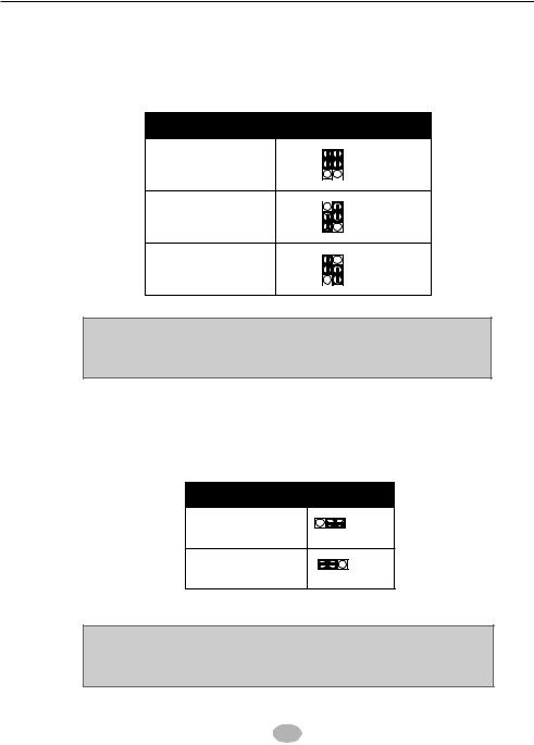
1


 4
4
JCD_IN1
JCD_IN1: CD ROM Audio Connector
PIN NO. |
JCD_IN1 |
|
|
|
|
PIN 1 |
Left |
|
Channel |
||
|
||
|
|
|
PIN 2 |
GND |
|
|
|
|
PIN 3 |
GND |
|
|
|
|
PIN 4 |
Right |
|
Channel |
||
|
30
Loading...