

Page 1
7151
COMPUTING MULTIMETER
MAINTENANCE MANUAL
Issue 1: June 1984
SOLARTRON
Schlumberger
Solartron pursues a policy of continuous development and product improvement
The specification in this document may therefore be changed without notice
Solartron Instruments, Victoria Road, Farn bo rough
Hampshire, England GU14 7PW Telephone: Farnborough (0252) 544433
Telex: 858245 Solfar G Cables: Solartron Famborough
A division of Schlumberger Electronics (UK) Ltd
PartNo. 71510011
19©84
Page 2

n
Page 3
7151 COMPUTING MULTIMETER
MAINTENANCE MANUAL
1642g/0072g
Page 4

Page 5
CONTENTS
Chapter 1
Chapter 2
Chapter 3
Chapter 4
Chapter 5
Chapter 6
General
Calibration Procedures
Dismantling & Reassembly
Circuit Descriptions & Diagrams
Fault Diagnosis Guide
Parts Lists &
Component Layout
1642g/0072g
Page 6

r
Page 7

Chapter 1 General
1642g/0072g
Page 8

f
Page 9
CHAPTER 1
1. GENERAL
The Solartron 7151 Computing Multimeter performs all common
functions, and offers: a library of
measurements;
The instrument is suitable for general purpose bench work, or for use
within a system where 7151 would
control interfaces. The interfaces provided are the IEEE 488 (1978) STD
system and the RS232C V24 serial system.
2. SAFETY
The 7151 multimeter has been designed in accordance with the
recommendations of IEC 348. To ensure the user's safety, and the
continued safe operation of the instrument, it is advisable to fully
observe the procedures and specifications given in the Operating Manual
(Part No. 71510010).
An Earth wire is provided to ensure the user's safety. Therefore, if an
extension mains cable is used, check that the Earth connection is
maintained throughout the length of the extension.
When using 7151 on
(e.g. inductive circuitry giving high back emf's such as
a large mains transformer), it is most important that 7151's test leads
are disconnected from the equipment before
that harmful back-emf's do not reach 7151. Care should
exercised when handling the input leads, especially where
are known to be present, or where
and a programmable power-on status.
equipment which is capable
programs;
be operated via
high transients could
clock controlled
one of
of delivering
switched it off. This ensures
measurement
its remote
high voltages
the secondary
always be
high
occur.
voltages
of
Whenever it is likely that the safety of the instrument has been impaired
- e.g. if it shows visible signs of damage, if it fails to perform
correctly, or if the specifications have been exceeded in any way - it
should be made inoperative and referred to a suitable repair depot. Any
maintenance, adjustment or repair of the multimeter must be carried out
by
skilled personnel only, in accordance with the procedures and
precautions detailed in this Maintenance Manual (part no. 71510011).
A
Wherever this symbol appears on the front or rear panel it is
advisable to consult the appropriate section of
further information.
3. SUMMARY OF OPERATION
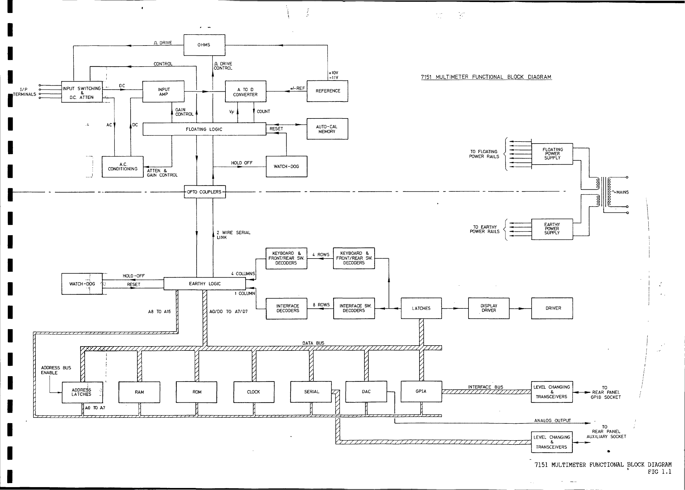
A schematic block diagram of the 7151 is shown in Fig. 1.1. 7151 is
essentially a
technique of analog to digital conversion.
All inputs to the instrument are first converted to dc voltages before
being passed to the input amplifier. This is simple enough for current
(dc) and resistance, but ac inputs also undergo rms conversion to dc.
All inputs are suitably scaled by the input amplifier and passed to the
voltage measuring instrument which uses the pulse width
the Operating Manual for
0072g/1634g
1.1
Page 10
analog to digital converter (ADC). With no input,
balanced pulse trains of
received, the
opposite
then
manner, proportional to the size of the input. These trains are
converted to a single end and gated into a reversible counter. The
mark-space ratios of the trains respond in an
mark space ratio 1:1. When an input is
the
ADC produces two
equal and
nett result is a pulse count proportional to the measure of the input.
The measuring circuits are controlled by what is termed the 'floating'
logic and
'Piggyback' ROM. The other circuits of 7151 are organised in a
arrangement which is controlled by the 'earthy' logic and consists
essentially
between the floating and earthy logic is acheived by
links. It is the
of
measurements, processing, remote
displays, and so
consists essentially of a 8-bit microprocessor
with
of another 8-bit microprocessor. Isolated communication
opto coupled serial
earthy logic
which is responsible for effective control
control, the real time clock, the
on.
bus
0072g/1634g
1.2
Page 11
A DRIVE
OHMS
I/P
TERMINALS »
CONTROL
A DRIVE
CONTROL
7151 MULTIMETER FUNCTIONAL BLOCK DIAGRAM
o-
INPUT SWITCHING
A.C.
CONDITIONING
INPUT
AMP
ATTEN. &
GAIN CONTROL
GAIN
CONTROL
FLOATING LOGIC
OPTO COUPLERS
CONVERTER
HOLD OFF
2 WIRE SERIAL
LINK
COUNT
RESET
+/-REF
WATCH-DOG
REFERENCE
AUTO-CAL
MEMORY
TO FLOATING
POWER
RAILS
TO EARTHY
POWER RAILS
FLOATING
POWER
SUPPLY
EARTHY
POWER
SUPPLY
ADDRESS BUS
ENABLE
WATCH-DPG
ADDRESS
LATCHES
At) TO A7
HOLD -OFF
RESET
A8 TO A15
EARTHY LOGIC
AO/DO TO A7/D7
4 COLUMNS
1 COLUMN
CLOCK
KEYBOARD 8.
FRONT/REAR SW.
DECODERS
INTERFACE
DECODERS
4 ROWS
8 ROWS
DATA BUS
SERIAL
KEYBOARD &
FRONT/REAR SW.
DECODERS
INTERFACE SW.
DECODERS
LATCHES
GPIA
DISPLAY
DRIVER
INTERFACE BUS
DRIVER
LEVEL CHANGING
TRANSCEIVERS
TO
■ REAR PANEL
GPIB SOCKET
ANALOG OUTPUT
TO
LEVEL CHANGING
TRANSCEIVERS
REAR PANEL
AUXILIARY SOCKET
7151 MULTIMETER FUNCTIONAL BLOCK
*
DIAGRAM
FIG 1.1
Page 12

Chapter
Calibration
Procedures
1642g/00'72g
Page 13

{
I
(
{
1
Page 14
CHAPTER 2
Setting-Up And Calibration Procedures
General
These procedures enable the instrument to be set-up
factory
despatch
standards
.
and
calibrated to the
The procedures are categorised into the following sections:
1. Setting-up procedures
2. Initial calibration
3. Final calibration
procedures
procedures
Safety
The instrument must be disconnected from the mains supply when
dismantling it to gain access to the preset controls and also
being reassembled (see
Chapter 4 for dlssembly instructions)
when it is
.
When adjusting preset controls beware of high test voltages, the guard
potential on the guard plate and also the mains input supply.
Calibration Method
Owing to the automatic calibration circuits incorporated in 7151, it can
only be calibrated by connecting it to a remote controller and then using
the appropriate calibration commands.
program can be used which is a
Solartron
can
supply, on tape cassettes, a calibration program for the
much faster method of calibrating 7151.
Alternatively, a calibration
more common types of controllers.
The user is advised to re-calibrate 7151 annually.
If the instrument's existing
satisfactory, the user can
constants by sending the REFRESH
state of calibration is judged to be
simply re-write the existing calibration
command to 7151 once it is in the
calibration mode.
Calibration Source
It is recommended that the calibration source has an accuracy of at least
two times better than the accuracy specified for the various 7151
functions. The 7151 specification is given in the Operating
Manual and
the important percentage accuracies are as follows:-
DC Volts
DC Current
AC Volts
AC Current
Resistance
0.002%
0.02%
0.05%
0.05%
0.002%
0072g/1624g
2.1
Page 15
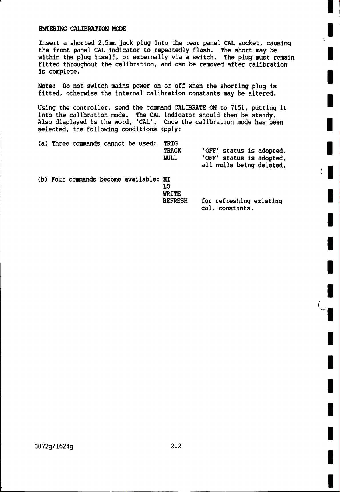
ENTERING CALIBRATION MODE
Insert a shorted 2.5mm jack plug Into the rear panel
the front panel CAL Indicator to repeatedly flash. The short may be
CAL socket, causing
within the plug Itself, or externally via a switch. The plug must remain
fitted throughout the calibration, and can be removed after calibration
is complete.
Note: Do not switch mains power on or off when the shorting plug Is
fitted, otherwise the Internal calibration
Using the controller, send the command CALIBRATE
Into the
calibration
mode. The
CAL Indicator should then be steady.
Also displayed Is the word, 'CAL'. Once the calibration mode
constants may be
ON to 7151, putting It
altered.
has been
selected, the following conditions apply:
(a) Three commands cannot be used: TRIG
TRACK
NULL
'OFF' status Is adopted.
'OFF' status Is adopted,
all nulls being deleted.
(b) Four commands become available: HI
LO
WRITE
REFRESH
for refreshing
existing
cal. constants.
0072g/1624g
2.2
Page 16
CALIBRATING MEASUREMENT RANGE
Using the controller, select the function and range to be calibrated by
sending the appropriate MODE and RANGE commands.
7151 must then be supplied with two precisely known reference inputs
(non-negative) one at approximately nominal full scale (referred to as
the Hi point), and
one at approximately zero (referred to as the Lo
point), in the case of ac ranges the Lo point should not be less than
approximately 5% of nominal full scale rather than zero. This ensures
that all inputs are within the optimum part of 7151's
linear range.
After a reference input is applied, 7151 must be informed of the precise
value of the input. This is achieved by using the HI command for a Hi
point, and the LO command for a Lo point. These commands must be
accompanied by an integer argument number, of up to six digits in length,
which expresses the applied input in terms of 5 x 9's count.
An integer value of 200000 corresponds to nominal full scale for any
range
For example, applying 2V on the 2V range, enter 200000
.
applying 20V on the 20V range, enter 200000
applying 5V on the 200V range, enter 005000
Apply the Hi point input to 7151 for the requisite function/range.
For example, 2.00843V on 2V dc range.
Using the controller, send the HI command to 7151.
For example, HI200843.
7151 responds by displaying 'Hi Pt' for about 1.5 seconds, during which
time it measures the applied reference input. When finished, the
instrument displays (and outputs) its measured count, e.g. 214576. It is
of no consequence if the displayed count differs from the applied input.
Repeat the above
(short circuit), and send the LO command. For example LOO (leading
zeroes need
Having
command
specified the Hi point and Lo point (in any order), send the
WRITE to 7151 (no argument required). This causes the
calibration constants for the selected range/function to be calculated
and
stored in memory. If successful, the message 'Good' is displayed.
If unsuccessful, an error message will be displayed and output to the
procedure for the Lo point. For example, reference = OV
not be specified).
controller.
Repeat the above instructions for each function/range to be calibrated.
0072g/1624g
2.3
Page 17
RESTORING THE MEASUREMENT FUNCTIONS
Using the controller, send 7151 the command CALIBRATE OFF. The CAL
indicator will then flash indicating that the CAL shorting plug is still
fitted.
Withdraw the CAL
shorting plug. The
CAL indicator should then be
invisible, the instrument being ready for normal use.
SUMMARY
(a) Insert CAL shorting plug (2.
(b) Select the calibration mode by sending the CALIBRATE ON
5mm) in rear panel socket
.
command.
(c) Select the requisite function and range to be calibrated and perform
the calibration sequence. Repeat for each range/function to be
calibrated.
(d) De-select the calibration mode by sending the
CALIBRATE OFF
command.
(e) Remove CAL plug.
0072g/1624g
2.4
Page 18
Setting-Up
Procedures
DC Power Supply Checks
Measure the dc supplies on PCB1 and PCB2 at the output pins of the
appropriate regulator IC's. Tolerances of the most important supplies,
mains voltage 240V, follow:
floating 15V unregulated
floating 15V regulated
floating 5V unregulated
floating 5V regulated
earthy 5V unregulated
earthy 5v regulated
between 20.7V and 21.6V
15 ± 0.75V
between 8.8V and 9.1V
5 + 0.25V
between 9.5V and 9.8V
5 ± 0.25V
Display Checks
The contrast of the display can be adjusted
by means of RV301. Make the
digits appear as black as possible but without introducing slurring when
a reading changes.
Keyboard Checks
The following sequence exercises all 16 keys.
Key Press
FILT 2 press minimum
Display Response
"FILT" on/off
Finish with "FILT" off
ma-
mA===
K£2
V~
V===
AUTO 2
V
A
LOCAL
presses
minimum
KQ
V~
V===
"AUTO" on/off
Check for downranging
Check for upranging
"GPIB nm" where nm is address
value.
NULL 2 presses minimuim
6x92
TRACK 2
presses
presses
minimum
minimum
SAMPLE with "HOLD" asserted
COMPUTE
MENU
"NULL" on/off
"6x9" on/off
"HOLD" on/off
“
HOLD" goes out briefly and
returns
.
"NO PROG"
“
PROBES?"
0072g/1624g
2.5
Page 19
Initial
Calibration
Procedures
Test Equipment
1. General purpose DMM.
2. General purpose oscilloscope
3. Controller, e.g. Commodore PET fitted with BASIC III or BASIC IV
firmware.
4. Calibrator, e.g. Fluke 5101 fitted with GPIB interface.
5. ACV Calibrator, e.g. Hewlett-Packard 745.
6. ACV High Voltage
7. Capacitor O.lyF polypropylene attached to a twin 4mm banana
(3/4" centres)
Switch on 7151 and
Amplifier e.g. Hewlett-Packard 746.
.
allow to warm up for at least one hour before
plugs
calibration.
The initial calibration
Table
2.1
No.
2.2
2.3
2.4
procedures are detailed in the following tables:
Procedure
Initial
Initial
Initial
Initial
calibration, DC
calibration, Resistance
calibration. Current
calibration, AC Volts
Volts
Please
Note: The limits of error expressed in the following tables are
those adhered to by the factory for a new instrument. As an instrument
'ages', "components become more noisy or their tolerances increase.
Therefore, when calibrating a used instrument, it may
be
necessary to
accept limits of error that are marginally higher than those listed in
these pages. However, the instrument should always conform to the
commercial specification (see Operating Manual) after calibration.
0072g/1624g
2.6
Page 20
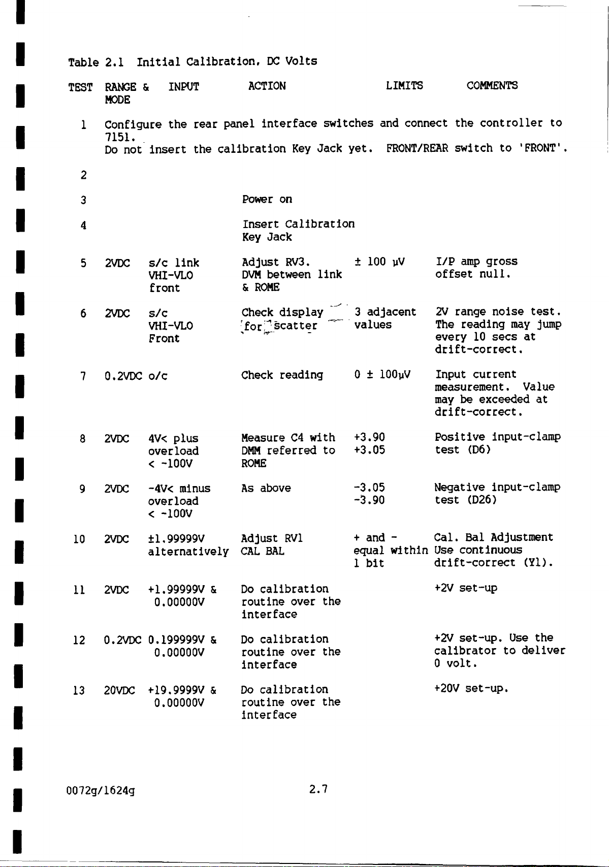
Table 2.1 Initial Calibration, DC Volts
TEST RANGE & INPUT
ACTION
LIMITS
COMMENTS
MODE
1 Configure the rear panel interface switches and connect the controller to
7151.
Do
not insert the calibration Key Jack yet. FRONT/REAR switch to 'FRONT'.
2
3
4
5
6
7
2VDC
2VDC
0.2VDC
s/c link
VHI-VLO
front
s/c
VHI-VLO
Front
o/c
Power on
Insert Calibration
Key Jack
Adjust RV3.
DVM between link
& ROME
Check display ^
'for2scatter
Check reading
± 100 yV
3 adjacent
values
0 ± lOOyV
I/P amp gross
offset null.
2V range noise test.
The reading may jump
every 10 secs at
drift-correct
Input current
measurement.
may be exceeded at
drift-correct
.
Value
.
10
11
12
13
8
9
2VDC
2VDC
2VDC
2VDC
0.2VDC
20VDC
4V< plus
overload
< -100V
-4V< minus
overload
< -100V
±1,99999V
alternatively
+
1.99999V &
0.00000V
0.
199999V &
0.00000V
+19.
9999V &
0.00000V
Measure C4 with
DMM referred to
ROME
As above
Adjust RV1
CAL BAL
Do calibration
routine over the
interface
Do calibration
routine over the
interface
Do calibration
routine over the
interface
+3.90
+3.05
-3.05
-3.90
+ and -
equal within
1 bit
Positive input-clamp
test (D6)
Negative input-clamp
test (D26)
Cal. Bal Adjustment
Use continuous
drift-correct (Yl)
.
+2V set-up
+2V set-up. Use the
calibrator to deliver
0 volt
.
+20V set-up.
0072g/1624g
2.7
Page 21
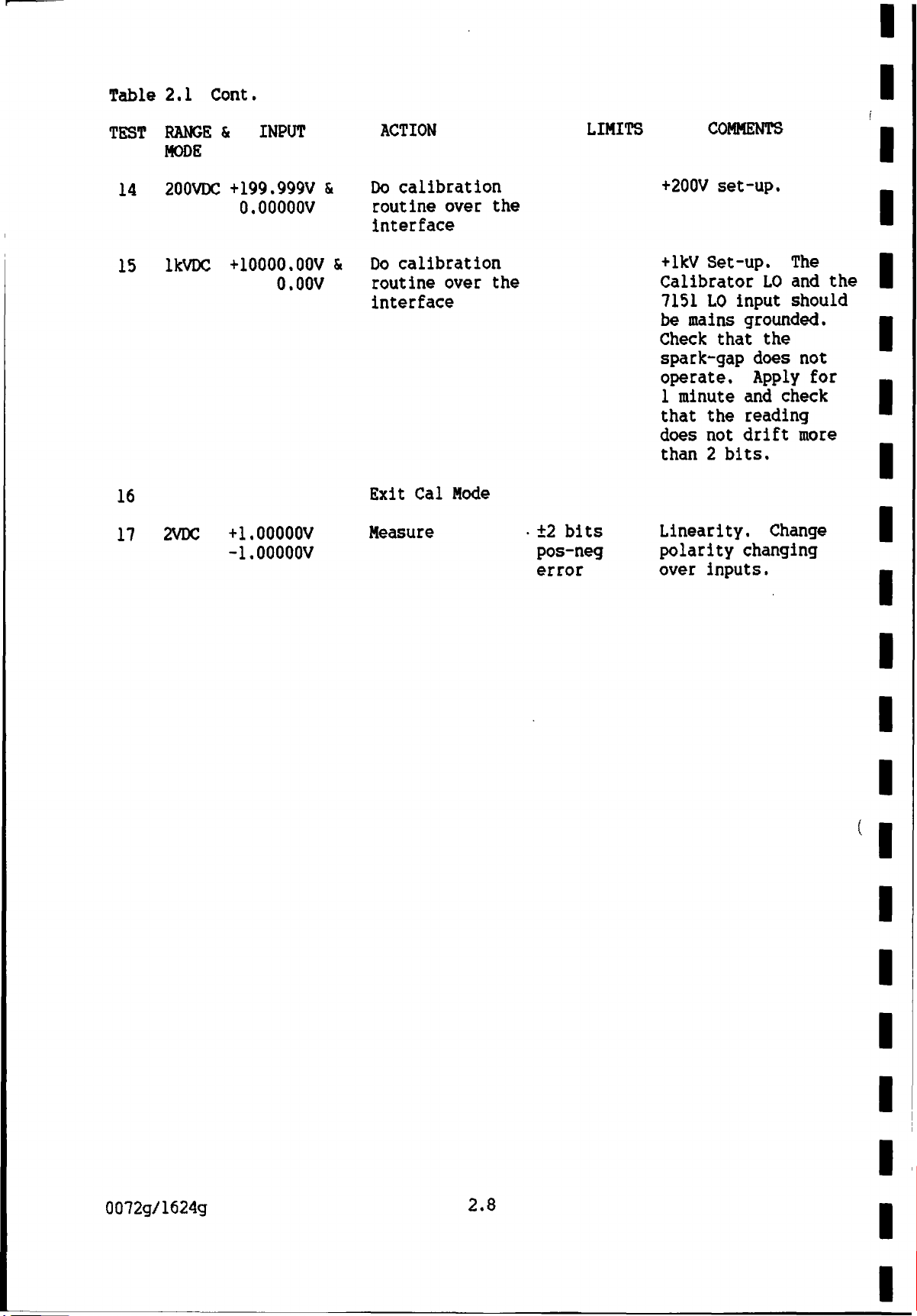
Table 2.1 Cent.
TEST RANGE & INPUT
MODE
14 200VDC +199.999V &
0.00000V
15 IkVDC +10000.
00V &
0.00V
16
17 2VDC +1.00000V
-1.00000V
ACTION
Do calibration
routine over the
LIMITS
COMMENTS
+200V set-up.
interface
Do calibration
routine over the
interface
+lkV Set-up. The
Calibrator LO and the
7151 LO input should
be mains grounded.
Check that the
spark-gap does not
operate. Apply for
1 minute and check
that the reading
does not drift more
than 2 bits.
Exit Cal Mode
Measure
+2 bits
pos-neg
error
Linearity. Change
polarity changing
over inputs.
0072g/1624g
2.8
Page 22
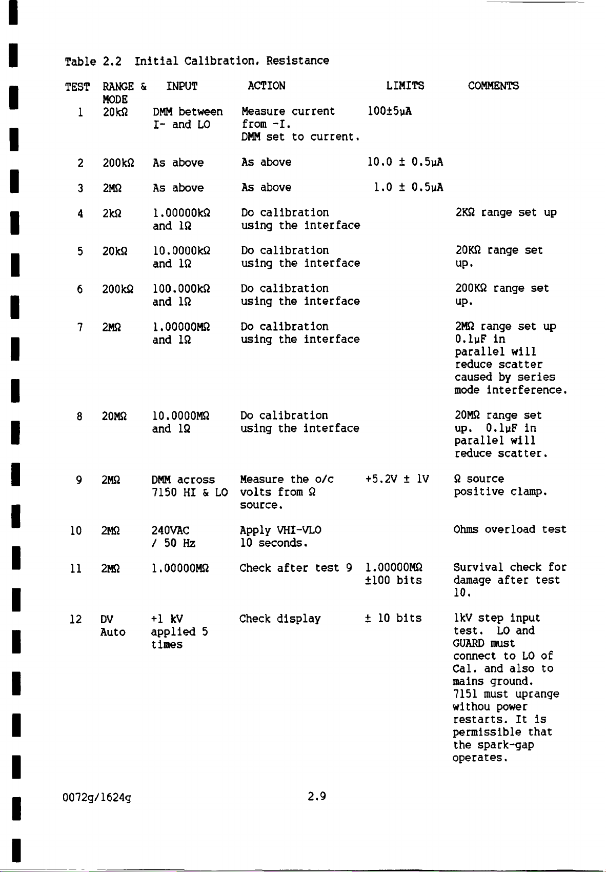
Table 2.2 Initial Calibration, Resistance
TEST
1
2
3
4
5
6
7
RANGE
MODE
20kfl
200kfl
2Mfi
2k£2
20kfi
200kfi
2Mft
5. INPUT
DMM between
I- and LO
As above
As above
l.OOOOOkfl
and IQ
lO.OOOOkQ
and IQ
lOO.OOOkQ
and IQ
1.00000MQ
and IQ
ACTION
Measure current
LIMITS
100±5yA
COMMENTS
from -I.
DMM set to current.
As above
As above
Do calibration
10.0 ± 0.5uA
1.0 ± 0,5yA
2KQ range set up
using the interface
Do calibration
using the interface
Do calibration
using the interface
Do calibration
using the interface
20KQ range set
up.
200KQ range set
up.
2MQ range set up
O.lyF in
parallel will
reduce scatter
caused by series
mode interference.
10
11
12
8
20MS2
10.0000MQ
and IQ
Do calibration
using the interface
20MQ range set
up. O.lyF in
parallel will
reduce scatter.
9
2M$2
DMM across
7150 HI & LO
2M£2
240VAC
/ 50 Hz
2Mfi
1.00000MQ
Measure the o/c
volts from Q
source
.
Apply VHI-VLO
10 seconds.
Check after test 9
+5.2V ± IV
1.00000MQ
±100 bits
Q source
positive clamp.
Ohms overload test
Survival check for
damage after test
10.
DV
Auto
+1 kV
applied 5
times
Check display
± 10 bits
IkV step input
test. LO
GUARD must
connect to LO of
Cal. and also to
and
mains ground.
7151 must uprange
withou power
restarts. It is
permissible that
the spark-gap
operates.
0072g/1624g
2.9
Page 23
Table 2.3 Initial Calibration, Current
TEST
1
2
3
5
RANGE
MODE
DC A
AC A
DC AC
& INPUT
+1.00000A &
open circuit
400 Hz
1.99999A &
0.19999A
+1.99999A
ACTION
Calibrate over the
LIMITS
COMMENTS
1 Ampere Set-up
bus
Calibrate over the
2 Ampere Set-up
bus
Exit Cal Mode
Measure voltage at
current front
sockets with
a
0.80 volt
Burden
DMM.
0072g/1624g
2.10
Page 24
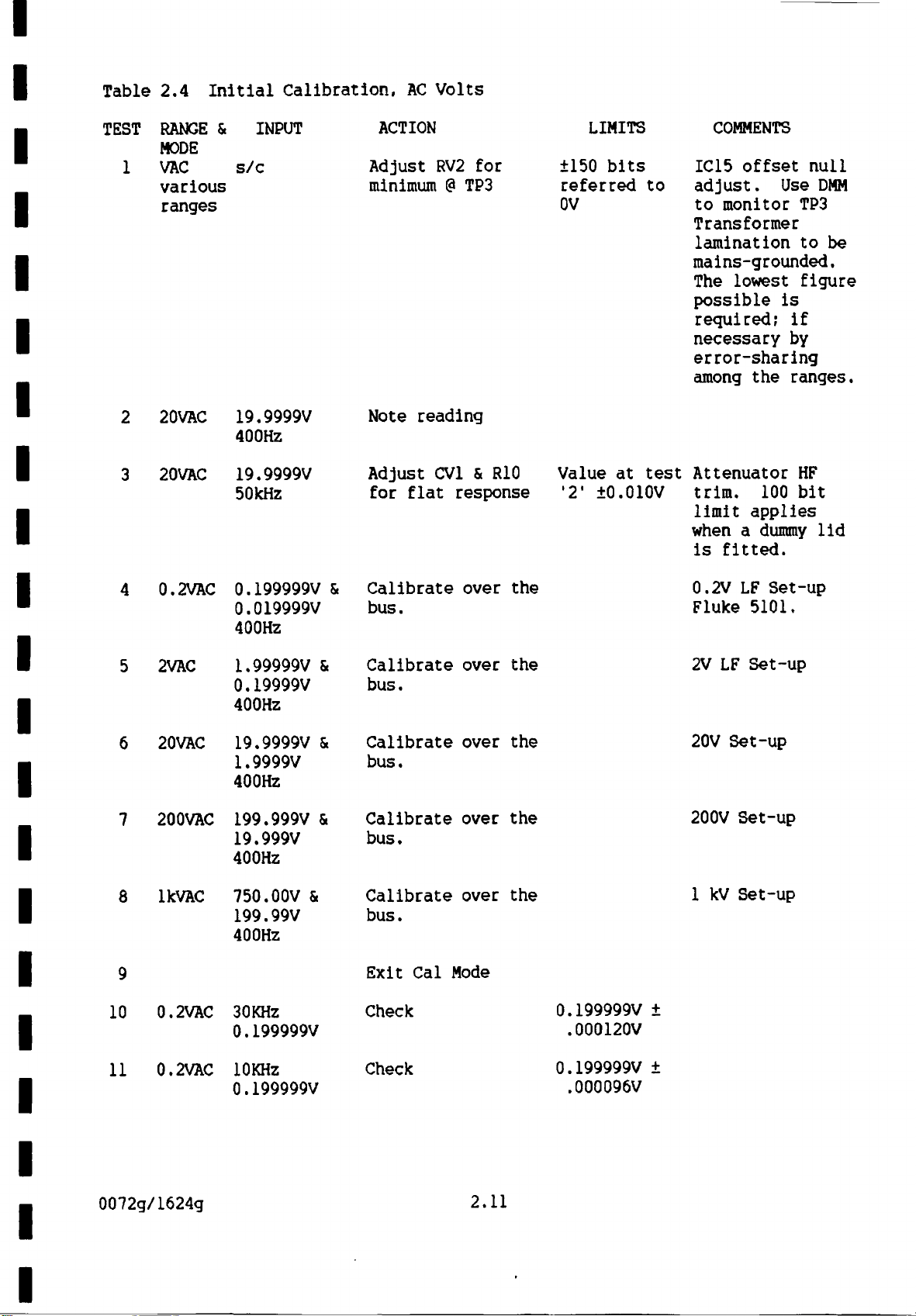
Table 2.4 Initial Calibration, AC Volts
TEST
1
2
3
RANGE &
MODE
VAC
various
ranges
20VAC
20VAC
INPUT
s/c
19.9999V
400Hz
19.9999V
50kHz
ACTION
Adjust RV2 for
minimum @
TP3
Note reading
Adjust CV1 St R10
for flat response
LIMITS
±150 bits
referred to
OV
Value at test
12'
±0.0
10V
COMMENTS
IC15 offset null
adjust.
to monitor TP3
Transformer
Use
DMM
lamination to be
mains-grounded.
The lowest figure
possible is
required; if
necessary by
error-sharing
among the ranges
Attenuator HF
trim. 100 bit
limit applies
when a dummy lid
is fitted.
.
10
4
5
6
7
8
9
0.2VAC
2VAC
20VAC
200VAC
IkVAC
0.2VAC
0.199999V &
0.019999V
400Hz
1.99999V &
0.19999V
400Hz
19.9999V S>
1.9999V
400Hz
199.999V S.
19.999V
400Hz
750.00V &
199.99V
400Hz
30KHz
0.199999V
Calibrate over the
bus.
Calibrate over the
bus.
Calibrate
bus.
Calibrate over the
bus.
Calibrate over the
bus.
Exit Cal Mode
Check
over the
0.
.000120V
199999V ±
0.2V LF
Fluke 5101.
2V LF Set-up
20V Set-up
200V Set-up
1 kV
Set-up
Set-up
11
0072g/1624g
0.2VAC
lOKHz
0.199999V
Check
2.11
0.
199999V ±
,000096V
Page 25
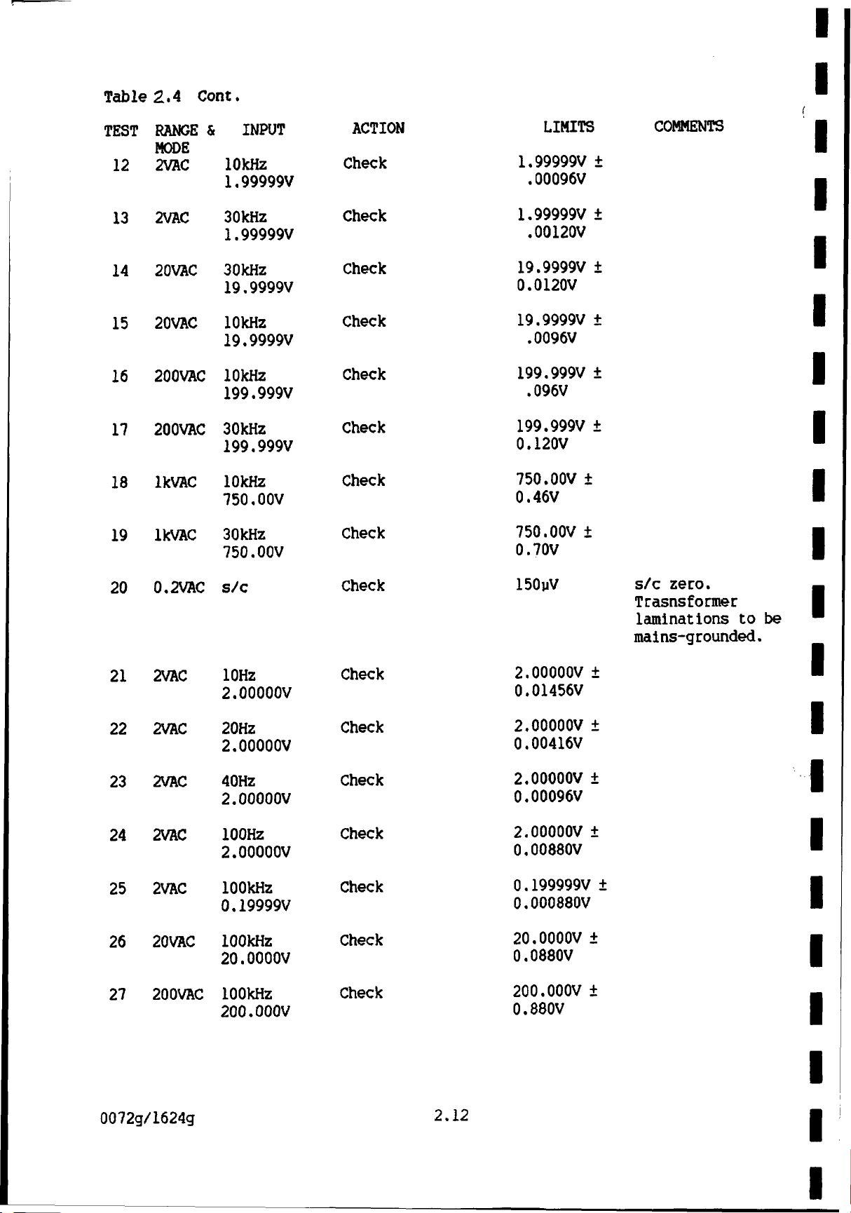
Table 2.4 Cent.
TEST
12
13
14
15
16
17
18
19
RANGE &
MODE
2VAC
2VAC
20VAC
20VAC
200VAC
200VAC
IkVAC
Ik VAC
INPUT
10kHz
1.99999V
30kHz
1.99999V
30kHz
19.9999V
10kHz
19.9999V
10kHz
199.999V
30kHz
199.999V
10kHz
750.00V
30kHz
750.00V
ACTION
Check
Check
Check
Check
Check
Check
Check
Check
LIMITS
1.99999V ±
.00096V
1.99999V ±
.00120V
19.9999V ±
0.0120V
19.9999V ±
.0096V
199.999V +
.096V
199.999V ±
0.120V
750.00V +
0.46V
750.00V +
0.70V
COMMENTS
20
21
22
23
24
25
26
27
0.2VAC
2VAC
2VAC
2VAC
2VAC
2VAC
20VAC
200VAC
s/c
10Hz
2.00000V
20Hz
2.00000V
40Hz
2.00000V
100Hz
2.00000V
100kHz
0.19999V
100kHz
20.0000V
100kHz
200.000V
Check
Check
Check
Check
Check
Check
Check
Check
150yV
2.00000V ±
0.01456V
2.00000V ±
0.00416V
2.00000V ±
0.00096V
2.00000V ±
0.00880V
0.199999V ±
0.000880V
20.0000V ±
0.0880V
200.000V ±
0.880V
s/c zero.
Trasnsformer
laminations to be
mains-grounded.
0072g/1624g
2.12
Page 26

Table 2.4 Cent
.
TEST RANGE & INPUT
MODE
24 2VAC
Auto
750V/400HZ Check
applied 5
times
ACTION
LIMITS
750.00 ±
0.46V
COMMENTS
750VAC
Autocange
test. Lo and
GUARD
must
connect to LO of
Calibrator and
also mains
ground. 7151
must uprange with
no signs of
distress.
0072g/1624g
2.13
Page 27

Final Calibration Procedures
7151 should be fully cased and
four hours and switched on for at least two hours prior to final
calibration. GUARD and LO should
placed in a
20,,C
environment for at least
be mains-grounded to minimise
series-mode interference. For this reason, use of the screened leads is
essential for HI fi measurement.
Note that the four screws which retain the top
be fully tightened to make the case screening
section of the case
effective.
must
The final calibration procedures are detailed in the following tables;
Table
2.5
2.6
2.7
2.8
2.9
2.10
No.
Final
Final
Final
Final
Final
Other
Procedure
calibration, DC Volts
calibration. Resistance
calibration, AC Volts
calibration, Current
calibration, Recheck
Checks
Q072g/1624g
V.
2.14
Page 28

Table 2.5 Final Calibration, DC Volts
TEST
1
2
3
4
5
RANGE &
MODE
0.2VDC
2VDC
20VDC
200VDC
IkVDC
INPUT
+0.100000V &
0.000000V the bus
+
1.9999V &
0.000000V
+19.
9999V &
0.000000V
+199.
+1000.00V
Sc
999V Sc
0.000000V
o.oov
ACTION
Calibrate over
Calibrate over
the bus
Calibrate over
the bus
Calibrate over
the bus
Calibrate over
the bus.
LIMITS
200mV range Cal. zero
volts to be
commanded from
Calibrator.
2V range
volts from
Calibrator on its 2
volt range.
20V range
volts from
Calibrator on its 20
volt range
200V range Cal. zero
volts from
Calibrator.
COMMENTS
IkV range
Cal. zero
Cal. zero
.
Cal.
0072g/1624g
2.15
Page 29

Table 2.6 Final Calibration, Resistance
TEST
1
2
3
4
5
RANGE &
MODE
2KS2
20142
200142
2M£2
20M$2
INPUT
1K$2 & IQ
10142 5. IQ
100142 &
IS
IMS &
IB
10MB &
IB
ACTION
Do calibration
over the bus
Do calibration
over the bus
Do calibration
over the bus
Do calibration
over the bus
Do calibration
over the
bus
LIMITS
COMMENTS
4 terminal connection
4 terminal connection
to be used.
Use screened lead
Use screened lead
0072g/1624g
2.16
Page 30

Table 2.7 Final Calibration, AC Volts
TEST RANGE & INPUT
MODE
1 0.2VAC 0.
2 2VAC
3 2QVAC 19.9999V
4 200VAC 199.999V
5 IkVAC 750.00V
199999V
& 0.0199999V
400Hz
1.99999V
& . 19999V <a
400Hz
& 1.9999V @
400Hz
& 19.999V @
400Hz
& 199.99V
400Hz
ACTION
Do calibration
over the bus
Do calibration
over the bus
Do calibration
over the bus
Do calibration
over the bus
Do
over the bus
calibration
LIMITS
COMMENTS
0072g/1624g
2.17
I
Page 31

Table 2.8 Final Calibration, Current
TEST
1
2
RANGE &
MODE
2ADC
2A AC
INPUT
1.00000A
and o/c
1.99999A
& 0.19999A
400Hz
ACTION
Do
calibration
LIMITS
COMMENTS
over the bus
Do calibration
over the bus
0072g/1624g
2.18
Page 32

Table 2.9 Final Calibration
Recheck (Filter In)
TEST
1
2
3
4
5
6
7
8
9
10
11
12
13
14
15
16
17
18
19
20
21
22
23
24
RANGE & MODE
2ADC
2AAC
2k®
20k$2
200k£2
2MS2
20MS2
0.2VAC
2VAC
20VAC
200VAC
Ik VAC
0.2VAC
20VAC
0.2VDC
2VDC
20VDC
200VDC
1 kVDC
1 kVDC
200VDC
20VDC
2VDC
0.2VDC
INPUT
1.00000A
1.9999A/400HZ
l.OOOOOKfi
lO.OOOOkQ
lOO.OOOkfi
l.OOOOOMfl
lO.OOOOMfi
0.199999V 400Hz
1.99999V 400Hz
19.9999V 400Hz
199.999V 400Hz
750.00V 400Hz
IQ (short circuit)
19.9999V 50kHz
+0.
199999V
+
1.99999V
+19.9999V
+199.
999V
+1000.
-10000.
00V
00V
-199.999V
-19.9999V
-1.99999V
-0.199999V
LIMITS
20 bits
100 bits
4 bits
4 bits
5 bits
5 bits
40 bits
100 bits
100 bits
100 bits
100 bits
46 bits
250 bits
300 bits
6 bits
6 bits
6 bits
6 bits
4 bits
4 bits
6 bits
6 bits
6 bits
6 bits
0072g/1624g
2.19
Page 33

Table
2.10 Other Checks
TEST
1
2
3
4
5
6
RANGE &
MODE
DC Auto
AC Auto
INPUT
1.5kV max.
See Fig.
See Fig.
25 Ampere
5 seconds
1.5kV rms
2.1
2.2
ACTION
Do flash test
Check
Display
Check Display
Perform earth
continuity test
Fit mains fuses
appropriate to
supply voltage.
Flash Test LO to
Earth.
LIMITS
0 + 500yV
0 ± 340yV
0.5Q
250mA SLO
BLO or 100mA
SLO-BLO
COMMENTS
Safety test to IEC
348. Refer to
Solartron
Specification
09/00/105.02. Power
switch
DC Common
ON.
Mode
Rejection 120dB.
AC Common Mode
Rejection 120dB.
As Test 1.
Q072g/1624g
2.20
Page 34

Figure 2.1 DC Common Mode Rejection
+ O
500V
Figure 2.2 AC
Mains O
Line
Common Mode
lOkfi
IkQ
Rejection
external
LINK
7 V HI
9
v
LO
^ GUARD
> V
HI
7151
MULTIMETER
7151
MULTIMETER
Ikfi
3 V LO
S GUARD
0072g/1624g
2.21
Page 35

Page 36

Chapter 3
Dismantling & Reassembly
1642g/0072g
Page 37

(
Page 38

CHAPTER 3
DISMANTLING AND REASSEMBLY
3.1 GENERAL
The 7151 must be disconnected from the mains supply before proceeding
with these Instructions.
3.2 DISMANTLING
1. Pivot the
carrying handle to the rear of the case. Pull out the
handle lugs from the pivot points on each side of the case and remove
the handle.
2. Remove the four screws from
the bottom of the case and then
withdraw
the top section of the case to expose the copper track side of PCB 1.
3. Compress the two plastic snap fasteners, located on
side of PCB 1 (as viewed from the unit front) to release the pcb.
Pivot the pcb outwards to gain access to the board components and to
the right hand
expose the screening pcb and the mains transformer.
4. Remove the two screws from the holes located in the mains transformer
laminations and withdraw the complete instrument assembly from the
bottom section of
the plastic stand-off fasteners which retain the screening
the case. PCB 2 can now be accessed by unclipping
board to
PCB 2.
5. At the left of the front panel assembly, remove the self-tapping
screw which secures the front panel assembly to a clip on PCB 2.
Unplug the front panel assembly from PCB 2.
6. To gain access to PCB 3, remove the six screws
to the front panel. Note that PCB 3 remains attached to the front
which
secure the pcb
panel by the keyboard ribbon cable.
3.3 REASSEMBLING
1. Fit PCB 3 to the front assembly using the six screws.
2. Carefully plug the front panel assembly into PCB 2. Check that all
of the connecting
pins on the front panel assembly are correctly
inserted into the socket pins on PCB 2.
3. Fit the self-tapping screw which secures the front panel assembly to
PCB 2.
4. Attach the screening pcb to PCB 2 by use of the plastic stand-off
fasteners.
5. Insert the complete instrument assembly into the bottom section of
the case. Insert the two screws into the holes on the mains
transformer laminations and tighten to secure the
bottom section of
the case.
00072g/1626g
3.1
Page 39

F
6. Secure PCB 1 by
use of the two plastic snap fasteners located on
right hand side of the pcb.
7. Dress the cables on the top
in the
board which locate the extended lugs in the top section
of the screening board clear of the holes
case.
8. Insert the top section
of the case onto the instrument assembly and
secure the top section to the bottom section by the four screws
inserted into the
bottom section
of the case.
NOTE: It is important that these four screws are fully tightened
otherwise the case screening is made ineffective and consequently the
ac calibration
9. Fit the
handle by lining up the locating lugs on the handle with the
could be impaired.
pivot points on each side of the case and then press the handle lugs
into the pivoting points on the case.
the
of the
00072g/1626g
3.2
Page 40

REAR PANEL SECTIONS
f
The instrument pictured is not 7151, but a similar instrument and is
intended only to show the functional assembly
.
7151
DISMANTLED
FIG 3.1
Page 41

Chapter 4 Circuit Descriptions & Diagrams
Page No.
4.1
4.2
4.3
4.4
Contents
General
Measurement of voltage, dc
Measurement of voltage, ac
Measurement of resistance
Measurement of current
Input amplifier
Drift correction
Input protection
Analogue to digital converter
Reference supply
4.5
4.6
1642g/0Q72g
Floating
Logic
Earthy Logic
Page 42

Page 43

CHAPTER 4
1. GENERAL
CIRCUIT DESCRIPTIONS AND DIAGRAMS
All multimeter inputs are at some stage processed
by the Analog to
Digital Converter (ADC) whose operating range is limited to ±2.6V. The
range of measurement is extended beyond this figure by
to the 2V range. For example, a
would
be seen by the ADC as only 2V. Non-dc inputs must of course
200V
input scaled
by a
scaling all inputs
factor of 0.01
undergo conversion to dc as well as attenuation and scaling.
2. MEASUREMENT OF VOLTAGE, DC
The dc voltage input attenuator consists of the resistors R1A to RID.
The attenuator is switched by FETs TR7, TR8, and relay
range control inputs from the floating logic. The attenuator setting,
RLK in response to
xl, xO.Ol, xO.OOl depends upon the selected voltage range, i.e.
Range(V)
0.2
,
2
20
,
200
1000
Attenuation
xl
xO.Ol
xO/001
Circuit Path
Direct to input amp. via RLE
RLK, TR7, with RLE open
RLK, TR8, with RLE
open
The attenuated outputs are then amplified by the input amplifier, whose
gain is arranged to
be xl or xlO to ensure satisfactory scaling at
the
ADC.
Input switching - The dc voltage inputs to the input amplifier are
selected via the series FET TR7 and the shunt FET TR6. With TR5 on, TR6
is off, and vice versa.
TR6 is switched
current measurement,
on during ac
and
during 'drift correct
(voltage or current) measurement,
'.
during dc
3. MEASUREMENT OF AC VOLTAGE
For Vac operations, inputs are first scaled to the 2V range
by the ac
signal conditioning circuits and then converted into a dc voltage.
AC inputs are subject to the ac input attenuator which is switched by
IC18, TR1, TR2, and by the op. amp. IC15. It's gain is set,
via IC18 to
be either xl or xlO. For inputs on the 2V range, no conditioning is
required; quad analog switch IC18 selects the gain of IC15 (via the
matched resistors R21A and R21B) to be set at unity, with inputs to the
amplifier passed through RLA, RLE and RLF contacts. The overall circuit
gain for other input ranges is selected by TR1 and IC18 in response to
range and control inputs from the floating logic.
Range(V)
0.2
2
20
200
1000
Attenuation
xl
xl
xO.Ol
xO.Ol
xO.OOl
Amp. I/P(V)
0.2
2
0.2
2
1
Gain
xlO
xl
xlO
xl
xl
Amp 0/P(V)
2
2
2
2
1
IC21. The
DC conversion is performed by the
true rmsto dc
maximum 2V output from this IC is switched to the dc input
converter
amplifier IC1 via the shunt input FET TR6 and via quad analog switch ICS.
1639g/0072g
4.1
Page 44

4. MEASUREMENT OF RESISTANCE
This is achieved by measuring the voltage developed across the unknown
resistance when a
voltage is then measured by the dc voltage measurement circuit.
Current Generator
IC3 is a
supply from the reference circuit. The
reference. Thus IC3 drives TR3, maintaining a IV differential across the
resistors R73, R74, R75 and R15. Control inputs from the logic circuitry
switch this resistor chain (via TR4, TR9, and
currents. The test currents for the various ranges are:
Mhen checking
available at the Hi ohms source terminal is returned via the Lo ohms
source terminal.
For the ranges other than 20MS2, the logic control, via IC2, also
switches in the resistor chain R7, R27 and R56
the Lo ohms source terminal and the -3.1V reference. This part of the
circuit acts as a calibrated
precision operational amplifier to
Nominal Range
20MQ
200k$2
20kS2
4-wire
Circuit
2MQ
2kQ
known
current is passed through it. The resultant
which is connected the +1QV
other amplifier input is the +11V
RLD) to define four test
Test Current
lOOnA
luA
10uA
lOOvA
lOOuA
measurement circuits ensure that all current
which is connected between
current sink for the test current generator.
Protection
R4 (22k) which is in series with both the 1+ and V+ input terminals.
Diodes D2 and D25 limit the
-2.6V.
5. MEASUREMENT OF CURRENT
This is achieved
resistance when the unknown current passes through it. The voltage
obtained can be measured by the dc input amplifier directly or for ac
inputs, via the AC-DC
DC Current Input
Resistor R3 is a 0.1$) shunt through
flows. The
via the quad switch ICS and shunt FET TR6. The gain
for dc current; the amplifier output is thus correctly scaled on the 2V
range for
AC Current Input
For ac inputs, the potential across resistor R3 is switched, via the quad
switch IC18 and FET TR2, to the ac operational amplifier IC15. The gain
of IC15 is set to xlO for ac current inputs; thus the inputs to the AC to
DC converter are scaled to the 2V range. After AC to DC conversion, the
output voltage is switched to the dc input amplifier via the quad switch
ICS and shunt FET TR6.
of the resistance
by
measuring the potential produced across a known
converter.
potential across R3 is switched to the dc input amplifier IC1
A to D conversion.
measurement circuit is provided by resistor
voltage of
TR3 and R4 to between +5.3V and
which the current to
be measured
of IC1 is set to xlO
Protection agains excessive current is by the 2A fuse, FI.
1639g/0072g
4.2
Page 45

6. INPUT AMPLIFIER
Input amplifier IC1 is a precision FET input operational amplifier.
Signals for IC1 are firstly amplified
by the dual FET pre-amplifier,
TR13, whose bias is provided by transistor TR14 and diode D7.
Inputs to the pre-amplifier are selected
(series FET) or TR6 (shunt FET) depending on the selected multimeter
function. For dc measurement functions (including resistance) TR5
either by switching on
TR5
conducts; for ac functions, or during drift corrections, TR6 conducts.
The gain of the pre-amplifier is controlled by IC2 in response to range
control signals from the floating logic. IC2 is a quad
analog
switch
connected across IC1 feedback resistors R18 and R19. The switching of
IC2 sets the overall gain of the pre-amplifier and IC1 to be xl or xlO
depending on the selected input range or measurement function. The gain
settings can be summarised as follows;
for DC
voltage
ranges
for DC
current range
Range (V)
0.2
2
20
200
1000
Range (mA)
2000
Gain
xlO
xl
xlO
xl
xl
Gain
xlO
for AC
current range
Range (mA)
2000
Gain
xl
7. DRIFT CORRECTION
A 'drift correct1 is
originating in the input amplifier or from
necessary in order to compensate for any drift
the ADC. Typically, drift
results from component aging or temperature fluctuations.
During a drift correct cycle, the input amplifier is isolated from any
measured input (series FET TR5 off) and connected to signal OV (shunt FET
TR6 on). With
due to drift. This is subsequently subtracted from a
zero input to the amplifier, any resultant count is then
measurement count
to provide a final count (i.e. result) free from error.
8. INPUT PROTECTION
Protection against voltage overload of the input amplifer is by spark-gap
SG2 (1400V nominal) which is connected across the VHI and VLO terminals.
Resistors R9 and R25 form a
current limiter, and
diodes D6 and D26 limit
series inputs to the amplifier to ±2.6V.
1639g/0072g
4. 3
Page 46

9. ANALOGUE TO DIGITAL CONVERTER (ADC)
This circuit converts the
digital pulses.
These
analogue output from
are used to gate
clock into a reversible counter
the input amplifier into
in the MPU, IC103, to produce a count proportional to the measured input
The Integrator
The integrator, ICS has the following inputs connected to its summing
point:
1. The input to
be measured
2. The forcing waveform
3. + reference or - reference
With zero input applied to the
waveform applied continuously to the integrator, the
alternately positive and
negative through the thresholds of the
multimeter and a 300Hz forcing square
output is driven
comparators IC9 and IC10.
The states of the two comparators are followed by the bistable, IC11
which
synchronises the transistors to a clock. The outputs from IC11
control the analogue switch IC16 which switch the + and - reference
supplies (through OV) to the integrator input. This closed loop feedback
arrangement ensures that the output is always dynamically balanced about
zero.
.
The synchronised output of the bistable, IC11, is also
passed to IC103 where the
pulses are counted.
NANDed by IC17 and
10. REFERENCE SUPPLY
This circuit generates the +10V
generator and the + and -3.1V supplies for the ADC. The reference
D20, together with the resistor network R38, R42, R17 and RV1, ensures
and +11V supplies for the ohms current
diode,
the input to IC4 is held at 3.1V. D20 also forms the + reference supply,
via IC6a and IC16, for the
ADC. The output of IC4 forms the -3.1V
reference supply.
All references are with respect to the 0V ROME.
The + reference voltage is also used as the input to IC6b. This is an
amplifier which drives a current through-R14, R57 and R16 in
order to
maintain the reference at balance. The resistor chain is tapped to
provide the +10V and +11V reference voltages for the
generator
.
ohms current
1639g/0072g
4.4
Page 47

11. FLOATING LOGIC
This circuit includes the floating logic microprocessor (MPU),
This IC communicates with the earthy logic MPU
via a 2-wire optically
IC103
.
coupled serial link. The circuit can be considered to have four separate
functions:
1. Controls range and
mode switching on
the analogue pcb.
2. Generates the forcing waveform for the ADC.
3. Counts the pulsed output from the ADC.
4. Stores calibration constants and checksum for use during auto-cal
procedures
Note:
The circuit automatically resets to a known state in the event
.
of a system lockout.
11.1 Analogue Control Lines
These MPU outputs are connected to drivers, comparators and bi-lateral
switches on the analogue pcb. The outputs, via their respective
switching
devices, correctly configure the circuits for the selected
multimeter range and function.
11.2 Forcing Waveform
The "timer-out"
generate the forcing
signal is converted into a 0 to 8V
signal from the MPU is a 300Hz waveform which is used to
waveform for the A to D converter.
square wave by
the bi-lateral switch
The TTL level
ICS in the analog circuit.
11.3 Counting Circuit
Timer-in is an input to the MPU which is derived from the ADC. The input
is a single, clock synchronised
alternatively, the length of
pulse-train; the pulse widths indicating
time the + and - reference voltages were
applied in order to balance the integrator. Within the MPU, these pulses
are used to gate clock into a reversible counter to produce a nett count
proportional to the measured input
.
11.4 Non-Volatile Memories
IC’s 105 and 106 are EAROMs which hold the automatic calibration program
for the multimeter and the calibration constants for each mode/range
selected.
11.5 Reset Watchdog
This circuit causes the floating MPU to be reset in the event of system
lockout.
The circuit operation is similar to that described for the
earthy logic reset circuit (page 2.11).
A 1.2288 MHz clock derived output from the MPU is divided by a 12-bit
binary counter IC 107. The 300Hz (3.33ms period) output from
this IC is
counted by the 4-bit counter, IC108.
The serial link TX DATA line from the ea
IC108. This input holds off the RESET output unless the RX DATA line is
inactive for more than 26.664ms (8x
period)
rthy
MPU, is also connected to
.
With the RESET line active, bistable IC112 (see ADC) is also reset,
thus
MPU pin 8 (TIMER IN) is set to a logic 1 state. Pins 8, 9, and 10 are
set to this state at initialisation.
1639g/0072g
4. 5
Page 48

12. EARTHY LOGIC
This includes the microprocessor set, the remote control interfaces, the
watch-dog reset circuitry, the analog to digital converter (analog
output),
clock and the interface switch decoders
.
MPU set
This consists of
IC 212 :
IC 207 :
IC 208 :
8 bit MPU
16K x 8 bit ROM
8K x 8 bit RAM
GPIB Interface
This consists of
IC 203 :
IC 202 :
IC 201 :
IC 203 consists essentially of 15
into by the
to RS2, 8 can be read by
MPU and, depending on the state of
the MPU.
The transceivers IC201 and 202 are bidirectional and consist of eight
driver/receiver pairs
each. Each driver/receiver is enabled by a
send/receive input (T/Rl and T/R2) with the disabled
general purpose interface adaptor
octal transceiver
octal transceiver
registers, 7 of which
control lines R/W and RSO
output forced to a
can be written
high impedance state. All GPU) signals are TTL level.
12.2 RS232 Interface
This consists of IC 204 : RS232 interface adaptor
IC 218 : RS232 line driver
IC 219 : RS232 line receiver
IC204 is essentially a
reversible 8 to 1 line decoder for the
transmission and reception of data via the TxD and RxD lines. IC218 and
219 serve to
buffer and level-shift the various signals to/from
RS232
levels (±12V).
12.3 Analog Output
This is generated by the 8-bit digital to
voltage
between the
Hi and Lo lines should bot exceed +10V, or be less
analog
converter, IC205. The
than OV.
12.4 Address
The
MPU addresses the various bus connected devices and the watch-dog
reset circuitry via the decoder, IC209. The ROM, IC207, is addressed
separately by the
Decoders
A15 (inverted) address line.
12.5 Clock
IC206 is a real time clock which is responsible for generating accurate
time signals for the MPU
and provides control signals for other
circuits. The clock frequency is factory adjusted to exactly 32.768kHz.
If the frequency is to
directly
across the crystal as this will produce a false reading.
Instead, the frequency
suitably buffered and divided by four. i.e. 8.1920kHz±0.1Hz. The
frequency can
be adjusted with C217.
be
checked, test probes must not be placed
should be
measured at
IC206/pin 21 where it is
Whilst the instrument is switched-off,
(pin 22) by the
1639g/0072g
back-up
battery, BAT 201 (approx. 4.5V).
standby power is supplied to IC206
4.6
Page 49

12.6 Reset Watchdog
This resets the MPU and the display in the event of a system lockout. A
0.6144MHz clock derived
12-bit binary counter IC216. The 150Hz (6.6ms period) resultant output
is checked
by the counter, IC217.
output from the MPU is further divided by
the
12.7 Display and Keyboard
This circuit has two main functions:
1. to decode display and command data
2. to transfer keyboard selections to the MPU
12.8 Display
The display circuit includes custom
undergoes selt-test for approx. 2 secs. The display is of the matrix
type
where it takes both column and
segments (see diagram of display layout).
pulses that alternate about 0V; this ensures that the crystals do not
LCD X301. At switch-on, the display
row
signals to activate
The display is driven by
particular
become permanently polarised.
The driver for the display is IC301 and is serially interfaced with the
'earthy* logic via pins 8->13. With CS (chip select), data can be sent
on the serial input (SI) line. A data bit is sent for every +ve going
transition of SCK; on the eight on, the BUSY line is made low until the
IC is ready to accept more data.
The serial input may just be data for display, in which case the control
data (C/D) line remains in its active low state. However, for driver
commands,
such as blanking or flashing the display, C/D is set to active
high.
12.9 Keyboard
The (vertical) column outputs from the keyboard are connected directly to
the
MPU and, with no selections made, held in the logic 1 state via
pull-up resistors on the earthy logic pcb. Keyboard (horizontal) rows
are scanned via output latch IC210 and BCD-to-decimal decoder,
IC302.
12.10 Power Supplies
Both PCB1 and PCB2 have on-board power-supply regulation, supplied by a
common
the regulated 5V
derived from PCB2's unregulated 5V
mains transformer. The display board logic derives its power from
supply
of PCB2
whilst the display backlighting
power is
supply. The -25V supply of PCB1 can
only be enabled by insertion or a shorted CAL plug, and is reguired to
re-program the calibration constants held in the EAROMs (ICs 105 & 106).
1639g/0072g
4. 7
Page 50

aep-fA*
Page 51

I
PCBl,
SHT 1 OF 3,
FLOATING ANALOGUE
DIAGRAM 4,1
Page 52

BROWN WIRE TO PHS01/11 O-
ORANOE WIRE TO PH50W3 1 O-
/ ^
PH >01
/I
fieo
WIRE TO PH601/?
YELLOW WIRE TO PH501K.
PH1Q1
IL
(
POWER SUPPLY
-cf>
C151
NEGATIVE
NON - VOLATILE
MEMORIES
270
)
IS CONNECTED
3 IS OPEN CIRCUIT
1
PIN NUMBERS
+ 5V OVP -5V -2SV
14
7,21
7
'6
*
-
'
-
>
-
6
-
7
-
-
-
■
-
-
P37 -
P36 i
P35 :
P34 -
P32 ■
P3I j
P30 ■
1C N« DEVICE TYPE
76LS04
10?
HO68P01VOS
103
- IC13/7
» TC14/A
S CONTROL
ANALOGUE
*35,106
107
*36
NC 7033
404066
74LS197
PCB1,
SHT 2 OF 3,
FLOATING ANALOGUE
DIAGRAM 4.2
Page 53

1C15I
-IC154
IC15I
IC152
1C156
!C153 h
,C,”o7
IC154
IC153
}FD
GROUND
GROUND
^OUTPUT
j
ICI55
IC1S7
WIRES TO PCS
2
j FLOATING'ANALOGUE POWER SUPPLIES
DIAGRAM
4.3
Page 54

?
5
l
1C214
k
5
5
i
IC215
♦SvfFLOATI
f
- BROWN WIRE
1
1
1
:
Opol7
i
|
-ORANGE WIRE
1C No
201,202
203
206
205
206
207
208
209
210
211
212
213
216
217
218
219
220
221
222
223
226
225
Type4
MC3667
MCS36B8
SY6S51A
A0558
HOU60I8
27128-6
HD6266P15
74US139
76LS376
76W5373
H06301
76LSH5
MC140408
74LS197
SN75190
SN75152
LM339
MCH071B
74 L
500
76L504
76 L5
03
MC16068B
PIN NUMBERS
ov
3V
24
12
20
1
1
IS
—
12
12
—
u
29
— —
16
20
10
20
10
21
1
16
B
16
8
14
—
—
12
—
7
14
16
H
7
16
7
-17V+
—
—
—
—
—
—
—
—
—
—
—
—
— —
9
—
—
—
—
—
—
12V
CMOS POWER
—
—
—
11
—
—
—
—
—
—
— —
—
—
6
16
—
—
— —
—
—
—
-
—
—
—
—
24
—
28
—
—
—
—
—
—
—
—
—
14
—
—
—
1C217
C232
OyOA7
IC222
1C223
1C22-
1
C228
0p0C7
C229
OpOA7
g>-
oe IC220d
SPARE GATES
po
ji>
ov IC221C
R207 NOT USED
PCB2, EARTHY LOGIC
DIAGRAM 4.4
Page 55

N2V SCHAFFNER FN372-2/
21
QRANQg WIRE
FUSES
SLO-BLO 1
1100/120: 250mA
220/240
:100mA
RED WIRE
> CABLE FORM TO PCBt
IC253
IC25!
IC251
IC257
1
I
i
i
i
DISPLAY BOARD
BACKLIGHTING
EARTHY LOGIC POWER SUPPLIES (5= MAINS POWER)
DIAGRAM 4.5
Page 56

UNRECULATEO
VOO VDO
IC303(A)
IC303;
T
i
acposs “
ins
fc
AKO 75F inoi
bi
isa'iosof
I
:c302
IC30I
LIQUID CRYSTAL DISPLAY X30I
PLUGS ATI SiO02 AND SK30;
IC302
anna
nnan
□□□□
□□□□
ARE NOT USED
Qe
FRONT VIEW OF PCS
f:ex!9l
£
C0NN5CTQ?
APPROACHES
SK1CLFPCM
THE RIGHT
PIN NUMBERING FOR FLEXI -CONNECTOR
KEYBOARD VlEV.EO
FROM FROfif <«<£ /PADl
□ □ □ □
FACE
□ □an
□ □ □ □
□ □ □ □
PCB3,
DISPLAY AMD KEYBOARD
DIAGRAM 4.6
Page 57

tDO
&
A
J LJ
-A
j
~7~
^
—7 ™
___z_____
nOA AUTO-HOLD FILT CAL NULL COMP ERR 6X0
7
4
50
26
backpl
ane
®
=
crossover
DISPLAY
DIAGRAM 4.7
segment
plane
WIRING.
Page 58

^T
OUTER SR&iO
nr
OUTER BRAIO
m
PCB1/0P6 AMI
PC8W0P2 VH[
PCBV0P5 GUARD
PCBW0P3 10
PCB1/0P1 H
PCBVDPA [-
, P/fi LOGIC INPUT
PC93/PAD'S'
TOP VIEW OF SWITCH
o 1
i
FRONT/REAR SWITCH
WIRING
DIAGRAM 4.8
Page 59

Chapter 5
Fault Diagnosis Guide
1642g/0072g
Page 60

(
Page 61

Chapter 5
Symptom
Possible Fault
Procedure
Instrument 'dead*
Fuses keep blowing
'Fail 1' displayed
at power-up
'Fail 2' displayed
at power-up
No mains power
A
good check is to look for the display
backlights. If no lights check fuses
and supply
Rectifier, regulator Correct current drawn from the
or smoothing
for 240V on 240V
voltages.
mains
setting: approx 60mA,
capacitor faulty. for 120V on 120V setting: approx 120mA.
Under fault conditions (regulator
blown) current may typically
be in
order of 500mA. Look for correct
output from each regulator IC.
Communication
breakdown
between
Check opto-couplers IC214 & IC215,
IC102, and the connecting wires and
floating and earthy plugs (to PCB 1). Look for activity on
logic
Problem with
Real- Leave 7151 switched on for 24 Mrs,
time clock IC206,
possibly caused by
battery BAT201 being and on again. If 'Fail 2' still
discharged.
the TX and RX lines.
displaying 'Fail 2', to recharge battery
(or fit a good replacement). Switch
displayed, switch off, remove turret
lug link (if no link, remove battery)
and momentarily
0V to reset the
short IC206 pin 22 to
chip. Also check that
pin 21 is exactly 8.192kHz (derived
from X203)
.
off
Amps range
'does not work'
Display inoperative
Display 'sluggish'
or too faint
7151 doesn't
perform 'correctly'
via remote control,
i.e. perhaps
occasional errors
occur.
2A fuse on rear
Check fuse,
panel blown.
Poor connections
Remake all connections and
verify 100%
between display and contact. Look for the following shaped
IC301, or of the
header PL301 in
socket SK204
waveform on the IC301 outputs
_
SCHS31:
.
Also check the control lines of IC301
(e.g. ensure that RESET is not 'stuck').
Display not
Check setting of RV301 (see P2.5).
correctly driven
Poor contacts in
switch S201, or
fault in interface
chips, IC201, 202,
203 (for GPIB)
or IC218, 219, 204
(for RS232).
Toggle switches S201 to clear their
contacts and set as required. If no
improvement check chips by substitution.
In the case of the
GPIB, ensure that the
correct cables are being used, and
disconnect all instruments other than
the controller to
verify if 7151 is
faulty.
1643g/0072g
5.1
Page 62

Symptom
Possible Fault
Procedure
After calibrating New cal. constants
7151, it is still haven't been stored
out of
Very
be very difficult to decide where to start looking. However, for PCB1 and
PGB2 there are some basic checks that can be carried out to
search.
Board
PGB 1
calibration, in IC105 & 106.
often a fault will not fall into one of the above categories and it can
Check
All power supplies are within tolerance (see Chapter 2).
Waveform E at
TX and RX of
pins 11 & 12. It is sufficient just to look for activity
on the signal lines.
Forcing waveform of 300 Hz is generated by IC103 pin 9.
Reference
-3.1V respectively.
IC103 pin 40 is 1.2288 MHz.
data from PCB 2 (via opto couplers) on IC103
voltages at IC16 pins 9 & 6 should be 3.1V
Check that -25V is produced
pin 5 when the CAL plug is fitted, and
that it reaches IC105 & 106 pin 1.
help narrow
by IC157
the
and
PCB 2
Waveform at TP4 (IC 16 pin 10) should look like:
|_
RESET from IC 103 pin 6 for activity.
etc.
(
All power supplies.
Waveform E at IC212 pin 40 is 1.2288MHz,
TX and RX of
pins 11 & 12. It is sufficient just to look for activity
on the signal lines.
RESET from IC212 pin 6 for activity.
Pin 21 of IC206 (Real time clock) should be
8.192kHz,
data from PCB 1 (via opto couplers) on IC212
exactly
1643g/0072g
5.2
Page 63

Chapter 6 Parts Lists &
Component Layout
Page
6.1
6.2
6.9
6.12
6.12
No.
Contents
Parts List abbreviations
PCB 1
PCB 2
PCB 3
Miscellaneous
1642g/0072g
Page 64

?ri
ir
no£j::e,yqz.:Zi
!?i f1;
5v."iJ i V
3bb;C
orj.'.'WT', t':r'
b.'j.uow. r- '
i.?C*
Page 65

CHAPTER 6
PARTS LISTS
AND LAYOUT
DIAGRAMS
INTRODUCTION
This section contains component layout diagrams and detailed parts lists
for each of the three printed circuit boards and the front and rear
panels. When ordering
spare parts, it is essential to quote the
instrument serial number located on the rear panel as well as the full
description
of the item given in the appropriate parts list.
A description of the abbreviations used in the parts list is given as
follows:
COMPONENT PARTS LIST ABBREVIATIONS
CIRCUIT REFERENCES
B
C
D
FS
IC
L
LK
PL
R
RL
S
SK
T
TP
TR
X
Battery
Capacitor
Diode
Fuse
Integrated
Circuit
Inductor
Link
Plug
Resistor
Relay
Switch
Socket
Transformer
Terminal Post (or Test Point)
Transistor
Other Components
Also Used:
RV
Variable Resistor
COMPONENT TYPES
Fixed Resistors
CACP
MEFM
MEGL
MEOX
POWW
PRWW
TKFM
Variable
CMPM
0072g/1636g
Carbon Composition
Metal Film
Metal Glaze
Metal Oxide
Power Wirewound
Precision Wirewound
Thick Film
Resistors
Cermet Preset Multiturn
Capacitors
ALME
CARS
GERM
ESTF
ESTM
PTFE
TAND
6,1
Aluminimum Electrolytic
Polycarbonate
Ceramic
Polyester Foil
Polyester Metallised
PTFE
Tantalum Dry
Page 66

r
PCS
l
(71510501) Floating Logic and Analogue
Cct.
Rl
R2
R3
R4
85
86
67 •
68
89 <
810
811
812
813
814
R15
816
817
818
819
821
Bef.
CAD
1776
Ik
0.1
22k
10k
1.2k
30.9k
100k
47k
990k
9k+lk
3.3k
Ik
1452 1
9k
CAD1776
10k
9k
Ik
9k+lk
J
0.25W
3W
0.5W
0.125W
0.125W
0.25W
3W
2W
0.2W
0.25W
0.25W
matched
P^lr
0.125W
matched
pair
0.2W
General Description
TKFM
5%
0.5%
5%
10%
0.5%
0.25%
5%
2%
0.5%
0.1%
5%
5%
MEOX
PRW
MEGL
CACP
MEFM
MEFM
MEOX
MEGL
MEFM
TKFM
MEOX
MEOX
0.25%
£
TKFM
0.5%
MEFM
0.25%
0.1%
TKFM
Solartron
Part No.
195631000
160300506
176442200
172341000
192731202
192843094
198651000
175244700
160400487
160400582
195633300
195631000
169617201
•
160400583
192741002
169617001
160400582
820
824
822
823
825
826
827
828
829
830
831
832
833
834
635
636
83?
838
R3y
840
100k O
67k J
33k
30k
47k
33k
' 280k
Ik
100
100k
100k
22k
Ik
100
4.7k
4.7k
470k
10k
33k
33k
matched
pair
0.25W
0.125W
3W
0.25W
0.
125V
0.25W
0.25W
0.25W
0.25W
0.25W
0.25 V
0.25W
0.25W
0.25W
0.5W
0.125W
0.25W
0.25W
0.25%
5%
0.5%
2%
5%
0.25%
5%
5% ?
5%
5%
5%
5%
5%
5% -
5%
10%
0.5%
5% t
5%
MEOX
MEFM
MEGL
MEOX
MEFM . ;
MEOX "
■ *
i-''
MEOX "J;
MEOX,x
meox
;;:
MEOX
MEOX :
MEOX
MEOX « ;
MEOX
CACP
MEFM =
MEOX -
MEOX
...
Ci
1
169617101
195643300
••
192743002
175244700
195643300
192852804
195631000
P
c
n
vy:
j
V
'\ ‘‘:
kS.
we.
VJcS.
Wf1"''1 -
i>r:, r
.
-
(t
‘
o
,
c
c
195621000
195651000
195651000
195642200
195631000
195621000
195634700
195634700
172354700
192741002
195643300
195643300
0072g/1636g
•1 e-V-
6.2
Page 67

PCB
Get.
R41
R42
R43
R44
R45
R46
R47
R48
R49
R50
R51
R52
R53
R54
R55
R56
R57
R59
R61
R62
R63
R64
R65
R66
R67
R68
R69
R70
R71
R72
R73
R74
R75
R76
R77
R78
1 (cont
Ref.
33k
100
4.7k
470k
100k
Ik
1M
100k
200k
1M
62k
33k
Ik
56
10k
2.7M
10k
27k
180
180
10k
22k
22k
82k
22k
22k
Ik
4.7k
15k
1M
10k
90k
900k
1.0M
1 .OH
1.0M
.)
0.25W
0.125W
3W
0.5W
0.25W
0.25W
0.5W
0.25W
0.125W
0.25W
0.
125W
0.25W
0.25W
0.25W
0.5W
0.25W
0.125W
0.
125W
0.25W
0.25W
0.25W
0.25W
0.25W
0.25W
0.125W
0.
125W
0.25W
0.125W
0.125W
0.5W
0.2W
0.2W
0.3W
0.25W
0.25W
0.25W
'
"' -
General Description
5%
0.5%
5%
10%
5%
5%
5%
5%
0.5%
0.5%
0.5%
5%
5%
5%
10%
10%
0.5%
0.5%
5%
5%
5%
5%
5%
5%
0.5%
0.5%
5%
0.5%
0.5%,.
5% '
0.25%
0.01% '
0.25%
10%
10%
10% x
HEOX
HEFH
HEOX . .
CACP
HEOX
HEOX '
HEOX . ;
HEOX''
HEFH
HEFH
HEFH • •0
HEOX '
HEOX
HEOX
CACP
CACP
HEFH
HEFH
HEOX
HEOX
HEOX
HEOX
HEOX
HEOX
HEFH
HEFH
HEOX
HEFH
HEFH
HEOX
PRWW r:
PRWW
PRWW
CACP
CACP
CACP
"
r
r--u;tc,r
'' ' •
w “
kcC.O
"
r--
-
r
:
.
k
w
-
V..
0
'■
;
-'*=
u' '3 '
192752002
198261002 «?
192746202V1
' 195643300^
195631000
195615600'-
172341000“13
172062700'"
192741004
192742702'
195621800^0
195621800 '»
195641000
195642200
195642200
195648200 -9
192742202
192742202 %
195631000 ^
- 192734702
192741502
193561000 Sfi
160300505 M
160300438 1
160300504
172061000 TJd
172061000
172061000
•
Solartron
Part No.
195643300
192721002 ^
193734700 Sfl
172354700 CH
!>2
195651000
195631000 «!H
193561000
195651000 'S
8A
1
ik
<sl2
'H
•*
^
"Sii
a6?
5T
5.T8
£%
-fl
R79
R80
R81
R82
0072g/1636g
1 .OH
100
100
33
0.25W
0.25W
0.25W
0.125W
10%
5%
5% f
0.5%’'
CACP
HEOX
HEOX
HEFH '
■r*
6.3
172061000
'■
195621000
195621000 v.-.
192713302
»*
Ur'
Page 68

PCS 1
(cont
.)
Cctl
R101
R103
R104
R105
R106
R151
R152
RV1
RV2
RV3;
RLA
RLE
RLC
RLD
RLE
RLE
RLK .
Ref.
,
15k
270
1.5k
100
100
47k
180
200
200k
2k
relay
relay
relay
relay
relay
relay
relay
0.25W
0.25W
0.25W
0.5V
0.25W
0.25 V
0.25V
0.5V
0.5V
0.5V
GOTO
GOTO
GOTO
GOTO
GOTO
4000
7002
7002
7002
4000
RS12
GOTO 7002-
General Description
5%
5%
5%
1%
5%
5%
5%
10%
10%
10%
MEOX
MEOX
MEOX
MEOX
MEOX "
MEOX
MEOX
multiturn
multiturn
multiturn
-0002
-5005
-5085
-5086
-0002
-5085
cermet preset
cermet preset
cermet preset
Solartron
Part No.
195641500
195622700
195631500
195421000
195621000
195644700
195621800
130922000
110016220
130932000
301203400
301203300
301203500
301203600
301203400
300652190
301203500
Cl
C2
C3
C4
C5, ,
C6
C7
C8
C9
CIO
Cll
C12
Cl 3
C14
CIS
C16
C17(0,
C18 ^
CIS ,
C20 \
C21
C22 ' 5
C23,
C24"1'
200pF
0.22vF
lOnF
470pF
22nF
15nF
0.47uF
0.22vF
15nF
47nF
47nF
lOOpF
47nF
47nF
47nF
luF
2.2yF
47nF
47nF
47nF
47nF
lOyF
.„t,.10yF
>1 6.8pF
500V
400V
1000V
400V
100V
100V
100V
400V
25V
25V
160V
25V
25V
25V
100V
100V
25V
25V
25V
25V
25V
25V
500V
20%
20%
10%
10%
10%
10%
10%
10%
25%
25%
20% >
25%
25%
25%
10%
10%
25%
25%
25%
25%
20% •*
20%
20%
GERM
ESTM
ESTF
ESTF
ESTM
ESTM
ESTM
ESTF
GERM r
GERM
GARB
germ
GERM ‘
GERM
ESTM *
ESTM *
GERM
GERM
GERM
GERM - •
TAND
TAND
3 GERM
241322200
226152200
222841000
208100201
222342200
225441500
225454700
225452200
222341500
—
241944700
241944700
#
v(u.
'
V f
v
ci
208900004
241944700
241944700
241944700
-
W*
\fri'
-S
V;-:
225461000
225462200
241944700
241944700
241944700
a
:
Vf
i
241944700
'•-
208700108
208700108
v';
"-
241306800
0072g/1636g
6.4
Page 69

1 (cont.)
PCB
•c-) I g>:
Get.
C25
C26
C27
C28
C29
C30
C31
C32
C33
C34
C3 5
C36
C37
C38
C39
040
041
042
C101
0102
Ref.
47nF
47pF
150pF
47pF
3.3yF
47nF
47nF
lOnF
lOnF
lOnF
lOnF
220pF
220pF
220pF
220pF
lOnF
47nF
3.3nF
33pF
33pF
0103 22uF
0104
0105
0106
0107
0108
0109
C110
0111
0112
0151
0152
0153
0154
0155
0156
0158
0159
0160
0161
0163
47nF
47nF
47nF
47nF
47nF
InF
47nF
47nF
lOOpF
2200yF
220yF
lOOOyF
470yF
lOOyF
lOOyF
lyF
lyF
lyF
lyF
lOOnF
25V
500V
500V
500V
100V
25V
25V
25V
:'lr.
25V
■ 25V
25V
500V
500V
500V
500V
25V
25V
-
500V
500V
16V
25V
25V
25V
25V
25V
500V
25V
25V
500V
16V
16V
40V
40V
25V
25V
35V
35V
35V
35V
50V
; General Description
25%
20%
20%
20%
10%
25%
25%
25%
25%
25%
25%
20%
20%
20%
20%
25%
25%
-
20%
20%
20%
25%
25%
25%
25%
25%
20%
25%»l>; GERM ,-,
25%
20%
-
-
-
-
-
-
20%
20%
20%
20%
20%
GERM
GERM
GERM
GERM
ESTM
GERM ,
GERM r!
GERM
GERM -.tv
GERM
GERM
GERM r.
ff/ija
GERM
GERM
GERM
GERM
- i;(
GERM
-
GERM
GERM
TAND
GERM
GERM
GERM
GERM r
GERM
GERM
L
£,
cerm
GERM
^
ALME -
j, ALME ' -
- ALME
ALME
; ALME
fc , ALME „ - -
TAND
TAND
.•:,
TAND
- i
TAND
G-.
<• '<
rCERM pulti layer,,
l1'.' j
vV f ", , V
kv 0
WC
.
. ' /
'
v
vr,;
.
-
v?;
v r„
vf
Solartron
Part No.
.
r
241944700 ,, ,
241314700 (,*
241321500. [y
241314700
225463300 r ..
241944700,
241944700,
241941000'
.0
_ v;-?
. 24i94iooo:,‘:
,
' 241941000 .wf
241941000 '
v,
241322200. ...
V
r m
241322200.;;,:
241322200
241322200
241941000
241944700 ^
208100207'
241313300
241313300
208700106 ^
241944700 ^
241944700 ....,
241944700
-
241944700
C..1
' 241944700"
241331000
241944700 /;'
.-iV
. 241944700:2
241321000
273392200,.
N
273382200
V
273791000 S
273784700
. 273581000
L-
n
273581000
f
26606
‘ 266061000
iood:;:'
^
,..266061000,.^
266061000,';.
2p845014p;?
'J'.iC .
t*w.v
0072g/1636g
6.5
'\F : CO
Page 70

PGB 1 (cont
ft ft*
Cgt. Ref
CV1
2-14pF
.)
General Description
PTFE
Solartron
Part No.
290060030
Dl
D2
D3 v '
D4
D5
D6 " V-;
xn
"v
D8 -
P9
Dl0> ;
Dll'
D12
D13
D15
D16
D17
D18
D19 ■
D20
D21
303
WR0 57
SD3
BZY 88
BZY88
WR0 57
IN4577
5.6V Zener 5%
8.2V Zener
5%
CO\ .
d
:
303
303
303
SD3
303
SD3
SD3
IN3595
IN3595
SD3
SD3
IN829A reference 6.2V Zener
SD3
400mtf
400mW
■ -
o
O
300522160
300525770
300522160
300521450
300521330
300525770
300525050
300522160
300522160
300522160
.
300522160
300522160
300522160
300522160
300523590
300523590
300522160
300522160
1
300525400
300522160
D22
D25'
D26
D27
D28
D101
D151
0152
0153
0154
0156
0157
TR1
TR2^
TR3r" '
TR4
f
TR5
TR6 '
TR7
TR8
303
WRO 57
WRO 57
BZY88 20V
SD3
SD3
W04
W04
IN4004
IN4004
BZY88
303
3N163
3N163
3N163
WN1001
WN1001
WN1001
PN4118A
WN1001
Zener
20V Zener 5%
' V ^ 1
5%
r * 1 . 1
Z iZ
Zl
C*
*' C.
* . A • 1 !
400mW
; j-.'3 ('*. , .
;
.
-Ticqte
400mW v?Bhta
. ' Acfv
A5.C
£ -
a
.
•
'
-.7
'3t5.V.'g vpf
£
.3
a;
-
'rt ^ Z
epz *E
?ic
i
vt:
Vc
\?>
'
•V "
VvIx>
'
^ ' u
^ 3 ■.
3v
V
300522160
300525770
300525770
300523790
300522160
300522160
300524700
300524700
300522070
300522070
300523790
300522160
300554530
300554530
300554530
300555770
300555770
300555770
300555880
300555770
0Q72g/1636g
Page 71

PCB 1
Get.
TR9
TRIO
TR11
TR12
(cont.
Ref.
)
WN1001
U1897
BCY70
WN
1001
General Description
I SD3
Solartron
Part No. ,
sziO
300555770
300553800.
vu
300553590
300555770 ifl
TR13
TR14
TR101
IC1
IC2
IC3
IC4
ICS
IC6
IC7
IC
8
ICQ
IC10
IC11
IC12
IC13
IC14
IC15
IC16
WD460
BC183
BC183
0PL4
DG211
AD545K
0P05
DG211
0P14
DG211
0P05
LM3I1
LM311
74LS175
LM399
ULN2003
LM339
AD528J
DG200
*■'
‘
Op. Amp (matched with IC6)
Quad
analog
SPST switch
Precision FET Op. Amp
Op Amp
Quad Analog SPST switch
Op. Amp (matched
with IC1)
Quad Analog SPST switch
Op Amp
Voltage
Comparator
Voltage Comparator
Quad D-type Flip-Flop
Quad O/Collector
Comparator
7-Channel Buffer
Quad O/Collector Comparator
FET Op. Amp
Dual Analog Switch
VS
300555820 Sd
1
300555590 ud
300555590
c
dd
rs 510091360 dG
510091180 fd
510090741 80
510091130
-L
5100911800 Id
510091360
510091180
510091130
510091280-
510091280-;
in
3
510003170 if:
510090490
510004980 ■ J
510090490 iG
510090380-
c
510091170
IC17
IC18
IC19
IC102
IC103
IC104
IC105
IC106
IC107
IC108
IC151
IC152
IC153
IC154
IC155
IC157
SGI
74LS00
DG211
AD637K
74LS04
Quad
Dual I/P
Quad Analog
Nand Gate
SPST switch
Rms to dc Converter
Hex Inverters
HD68P01V05 Microprocessor
6.8k$2
Resistor pack
NC7033
NC7033
4040 BE
74LS197
7515CKC
LM340T5
79L05ACZ
7915
79L05ACZ
TIL117
12
stage ripple counter
4 bit binary bounter
15V
5V
5V
15V
5V
0.5A pos. volt reg.
0.5A pos. volt reg.
0.1A neg. volt reg.
0.5A neg. volt reg.
0.1A neg. volt reg.
Opto transistor 300540240
Ceramic surge voltage protector, 1400V
510002000 -c!
V-.V
510091460
510091460
g
g
510002690
510006250
160400569
g
510005150 :c
510005150
' 510001820 id
t
-
510005750
;a
510090320 id
510090500
51009095QL3
51009033bn-n
rr 510090950^•
: i? 30001147^-1
ji'".r-
\g
‘
’.
’
0072g/1636g
6.7
"J&
Page 72

PCS 1
(cont.)
Cctf Rofi
j/
FH1
f
PHI 51
X101
• - - i
,
20mm x
5mm
Fuseholder
20mm x 5m 2A
8-way header,
Fuse
C General Description
0.1" pitch
4.9152MHz crystal. 30pF 0.01%
.
V- " '
*.
S' ;:j. » ; f i
'VeV
Solartron
Part No.
360206040
a
r-s i
360106150
352308060
300810590
TPl
TP2
TP4
OJO:.
T*\ ^
W ‘
VI
?
p
•Vr
Test hook
Test hook
Test hook
;
r>'
r ‘
t*' * r
< - •
355400760
355400760
355400760
:
i-C*
.
;;
* ' . U
nd,'
r'i
C*D
0072g/1636g
.
,•
} »• < r sw1' ■ ‘ "i
*
• ..
^
;
•if.Orl v'i*
1 :
^ k««
” 3-
-
/‘C
(i
w?:., o
Wf i.
enj?q
Vi
J
0
.
.
’ .M
j't'.V
; ■ ,.Oi ■ '..T . .
,
v0v3
(ej'ie ‘
i-
:
C ',c
.
-,r
X
V •
v
:-:r.
1
;
^ sf:*:;}ty
V,
Vs..
6.8
Page 73

2Zf-
5frLl-
f
£35
Get. Ref
SK201
SK202
SK203
Auxiliary
Socket (with ribbon)
GPEB Socket
CAL Socket
Fuse, 2A Fast blow
Fuse, 250mA slow blow
Fuse, 100mA
slow blow
General Description
*-■
fi
-/'j::
a
"-
M
um
SOI
f '-'S.
•p
/'f'v
‘a: :
Vc- „ V
wes.'i
V ‘"v
■- :
,;0d
Vi).-.:
seefr-SBoegn .
'-C '"V
•
CiOC
sr.: ' ; ,
•:;
> ■■
,:
i0c<5/
Solartrpn
Part N6.
71510205B
352524320.^>
352501740
360106150 iV,
_360106260
o-;:
f1
x
;
a-: /’
'u, '. sj
:
sj
:•=- ' 1
riM
rein
30 5^1
VO]
:apv*
iOcD
loca
mo
iOCQ
POLO
1008:'
1
,
.0031
vOtOl
;0£D1
rno?7.
nr :
v.v • ■
■ y> v’
C";
>T(T.(V *
rzift1
' y >i DOS toB? Ot
rvv • twe
2L<0^fibj Jeo-:!11! •. - 5<5 ^698
]r-;<v05 iKiKiJ b&a
mm!> ;
tf.'S
: ro-?
' ‘^“Oo
: J' "uqni ir.’.sh
wj-.' rrs-^iC
rn'O1’
wr
ilyX
r-.f. ? .<■
v
iasK
0072g/1636g
3Sf.r
'Op.P--;?
.q
6.13
Rnir
::A:-.pn'oo
Page 74

{
I
(
{
1
Page 75

PGB 2 (71510502)
Get. Ref.
R201
R202
R203
R204
R205
R206
R208
R209
R211
R212
R213
R214
3.3k
Ik
Ik
220
220
Ik
150k
4.7m
470
15k
12k
12k
0.25W
0.25W
0.25W
0.25W
0.25W
0.25W
0.25W
0.25V
0.25W
0.25W
0.25W
0.25V
. General Description
5%
5%
5%
5%
5%
5%
5%
10%
5%
5%
5%
5%
MEOX
MEOX
MEOX
MEOX
MEOX r .
MEOX "q‘
MEOX
CACP
MEOX
MEOX
MEOX
MEOX
: -195631000
J'OO.I
.hOOfj
‘ -
.r^yL
Solattron
Part No.
195633300
195631000 ’ H'H
195631000
195622200
: MS
195622200
195651000
172064700 V?'l
195624700^'^'
-'IX
i'r
’
195641500
195641200
195641200
R215
R216
R217
R218
R219
R220
R221
R222
R223
R224
R225
R227
R228
R229
R230
R231
R232
R233
R234
R235
270
Ik
6.8k
68k
33k
18k
3.3k
1.5k
3.3k
3k
2.2k
2.2k
6.8k
68k
6.8k
Ik
Ik
1M
6.8k
6.8k
0.25V
0.25V
0.25V
0.25V
0.25V
0.25V
0.25V
0.25V
0.25V
0.25V
0.25V
0.25V
0.25V
0.25V
0.25V
0.25V
0.25V
0.5V
0.25V
0.25V
5%
5%
5%
5%
5%
5%
5%
5%
5%
5%
5%
5%
5%
5%
5%
5%
5%
5%
5%
5%
MEOX
MEOX
MEOX
MEOX
MEOX
MEOX
MEOX
MEOX
MEOX
MEOX
MEOX
MEOX
MEOX
MEOX
MEOX
MEOX
MEOX
MEOX
MEOX
MEOX
195622700
195631000
195636800
195646800
195643300
195641800
195633300
195631500
195633300
195633000
195632200
195632200
195636800
195646800
195636800
195631000
195631000
193561000
195636800
195636800
R251
C201
1M (on
47nF
through
C215
0216 33pF
C217
C218
C219
0220
0072g/1636g
2-27pF
33pF
33pF
33pF
rear panel)
40V
500V
(variable)
500V
500V
500V
20%
film
20%
20%
20%
25%
GERM
GERM
GERM
GERM
GERM
6.9
172361000
241944700
241313300
290030280
241313300
241313300
241313300
Page 76

BCB 2
Get, Bef. -
C221 -
C222
0222
C224
(cont)
asr-zx-.
InF
47nF
47nF
lOnF
O' ?
C225'
C226
C227.v\
0228
0229 ?
0230
0232.r ..
0235
0236
0237
0238
0239
l.OnF
lOOuF
47nF
lOOnF
47nF
47nF
,.47nF
47nF
47nF
InF
InF
InF
.> .v
0240
C2Si
0252 .
C253
100pF
2200yF
,2200yF
470yF
'v‘'. •
0254
'if-
D2Qi^;
D202
D263
D204 ,
D205
D206
D207
D208
470yF
v
1N6263
1N6263
1N6263
1N6263
1N825
4.7V Zener
4.7V Zener
SD3
sr-.-ip. • , „
General Description
Solartron
Part No.
241331000
500V
25V
25V
100V
100V
10V
25V
50V
40V
40V
40V
40V
40V
500V
500V
500V
20%
25%
25%
10%
10%
20%
25%
20%
25%
25%
25%
■V-‘‘ .
25%
20%,
20%
20%
UhKM
.
/
■■ tr-**^,*
CERH
GERM
>•-?
ESTF
<’>-• l} -f
ESTF^.;,.
TAND 4,^, tsIWC* W'
GERM (multilayer)
: •“i ; ."r
OERM
^ r
j g- . ^
GERM
CERM
ir
GERM
CERM j,;, ^
GERM
-r, - ^
GERM '
;>#•
^
,•< r*- -« ?•••• i
jjx- 5
g,
.i
-
U':
iVi'
refi
241944700
241944700
227041000
227041000
265481000
241944700
208450140
241944700
241944700
241944700
241944700
.
241944700
241331000
241331000
241331000
■' ! ;;
500V
16V
16V
40V
40V
20%
CERM
■
ALME - ■;
ALME . i - f .
ALME
^ .. << . . .
~}i
* iA-iv «v
-
i J »'''
ALME
: .
i
241321000:
273392200
273392200
273784700
273784700
300525650
300525650
300525650
“i.
> v
-V- ,
■■
■ 'J #'•
.Oi--'
?
Ai,C'
-1
-
-f
V
V£.
‘
;;
'i- .
300525650
300523050
300521470
300521470
300522160
D251
D252
SW201
BAT201
X201
X202
X203
PH201
PH202
TPl->7
0072g/1636g
W0 4
W04
Bridge
Bridge
Rectifier
Rectifier
8-way Interface configuring switch
3.6V Battery
4.9152MHz Crystal
1.8432MHz Crystal
32.768kHz Crystal
4-way Header
2-way Header
Test Hook
6.10
300524700
300524700
375000600
800400210
300810590
300810460
300810640
352304080
352302080
355400760
Page 77

PGB 2 (cont)
Get. Ref.
IC201
IC202
IC203
IC204
MC3447
MC3447
MC68488
SYP6551A
General Description
,Z
'
8 way trance!vers
8 way trance!vers
GPIB Interface adaptor ^
EiS232 interface^
:'1'
•v.-o'. £ £>£
Solart ton
Part‘No.^idb
510005700
’
510005700
^
510006090&t'
IC205
IC206
IC208
IC209
IC210
IC211
IC212
IC213
IC214
IC215
IC216
IC217
IC218
IC219
IC220
IC221
IC222
IC223
IC224
IC223
IC226
IC227
IC251
IC252
IC253
AD558
HD146818
HM6264P15
74LS139
74LS374
74LS373
HD6303
74LS145
HCPL2601
HCPL2601
MC14040B
74LS197
SN75150
SN75152
LM339
MC14071B
74LS00
74LS04
74LS03
MC14068B
6.8k
100k
LM240T5
78L12
79L12
8 bit digital to analog converter ^
Real time clock" ;
64k static RAM
2 to 4 line decoder
■/; *• ;: v
Octal latch/Flip-flop
Octal tri-state”
[ 1
/>-^5$
latch
’
’
'pi
^
i/d?
8-bit microprocessor ^"{*
BCD to decimal decoder/tiriver V^#v
w *" • 1
Opto-coupled transistor
Opto-coupled transistof 3
12
-stage ripple counter J,
4-bit binary counter
EtS232 line
driver
RS232 line receiver
Quad
0/Collector comparator
Quad dual i/p
Quad
dual i/p Nand Gate
Hex inverters
Quad
dual i/p Nand gate
8-input Nand
Resistor pack
OR gate
gate
s. v<
X Vt*
■■■
’
3'*
v:
''Cf1?
!
'1
-
Resistor pack
5V
12V
12V
0.5A
0.1A
0.1A
pos. volt
pos. volt
neg. volt
reg.
reg.
reg.
510091430
“
510006300^3
v- 510006500.^
v 51000296(FtO
*rC "
510004390
'‘•51000487&£v
9/r
S'5M004990LS2$
*9.' "t
300540260
300540260'
510001820:\t'
510005750.’^
510005250
‘
'51009049DUK-
51000168»$i>
V;"
'
510002000
' - 510002690?^
510004140
510002630r>;C
(ri." r'.
• 16040056957
. 160400598
510090500
510090450x3
iwv-5 V
‘,,'51009046»;f5
i t
'&&&
■
5
“
’
>
0072g/1636g
■ \ i
Vv
*
6.11
M.
V ~ '
’t 6
r:? ■ <■
J \1 ? ^
Y'ji-j:, .
.r‘‘
5vin r'-B1- .
,
■?1
-Y-
1
- ->0!
■?
Jk '
Y&v-
- -x
a
Ih-tslAt
V5?;x
5651$
> OxF
n
iOShyl
’“'■i'-.T
Page 78

PCS 3 (71510503) Display Board
Gct.ncRef
R3oi:f
• '' '
,0
180k
R302"; "x1.8k
560
R303
R304 • •'
,v
R305 ;t • '
R307
R308
RV301
C301
C302
D301
D302
D303
D304
270
270
560
47
2k
O.lyF
O.lwF
LED, HP5082-4558
LED, HP5082-4558
LED, HP5082-4558
LED, HP5082-4558
light guide for D30H304
TR301
BCY70
!
\
General Description
Solartron
Part No.
0.25W
0.25W
0.25W
0.25W
0.25W
0.25W
0.25W
0.5W
50V
50V
5%
5%
5%
5%
5%
5%
5%
10%
20%
20%
MEOX 1* •'-■'w)
MEOX
MEOX
MEOX
MEOX
v.ffjrOOi
MEOX
MEOX
multiturn preset
GERM
GERM
:■
,'iC' Vi'1" I :
V36
is/-.
"s'-
L>
'lHC'7.r
195651800
195631800
195625600
195622700
195622700
195625600
195614700
130632000
208450140
208450140
300750270
300750270
300750270
300750270
71502035B
300553590
IC301
XC302
IC303
KB301
X301
NEC7225G
74LS145
316B 6.8k Resistor pack
Keyboard
Matrix (with ribbon)
Liquid Crystal Display
Front Panel
Red 4mm socket
Black 4mm socket
Green 4mm socket
Brown 4mm socket
Front/Rear switch
Rear Panel & Miscellaneous
Red 4mm socket
Black 4mm socket
Green 4mm socket
Yellow 4nm socket
N251
3251
Mains input unit
Mains switch
510005890
510004990
192136800
71512000
352501470
352501480
352501490
352501750
71517001
352501470
352501480
352501490
550001480
375500020
T251
0p72g/1636g
Mains Transformer
309618901
': ’5 6.12
Page 79

016 R37-
MOS-AVOID STATIC
K TR6
‘mo'.
;
f-2 ans?
1P4
BLUE
0P3 BLACK
YELLOW '
DP5
OREEN
v
5
'<
> V -
V
CI0 7
C10I
IC
103 IN SK
ir ICS
RIOS
RIOI o |
103
R 103
IC
102
IC
105 IC
SOLARTRON
I C
104
106
sp,
IC 108
TPI .
IC
RIM
0157
107
ICI57
LD
o o o
^PS
'
brown
'IV ?
"l (
O'.
;■
‘
L
ly.
i
i
ff!
PCB 1 COMPONENT LAYOUT
FIG 6.1
Page 80

IC224
TP7 TPS
EFTXEFRX
— in ------------------------------
C220 dp
C2I9
IC203
—
PCB 2 COMPONENT LAYOUT
FIG 6.2
Page 81

i
oca
zocai
*
PCB 3 COMPONENT LAYOUT
FIG 6.3
Page 82

 Loading...