


查询USB97C202供应商
USB97C202
USB 2.0
ATA/ ATAPI Controller
Datasheet
Product Features
2.5 Volt, Low Power Core Operation
3.3 Volt I/O with 5V input tolerance
Complete USB Specification 2.0 Compatibility
− Includes USB 2.0 Transceiver
− A Bi-directional Control and a Bi-directional Bulk
Endpoint are provided.
Complete System Solution for interfacing ATA or
ATAPI devices to USB 2.0 bus
− Supports USB Mass Storage Compliant Bootable
BIOS
− Supports ATA6 Drive capacities up to 2048GB
− True UDMA Mode 4 transfer rates
− Support for ATAPI Devices:
- CD-ROM
- CD-R
- CD-RW
- DVD
- DVD/R/W
8051 8 bit microprocessor
− Provides low speed control functions
− 30 Mhz execution speed at 4 cycles per instruction
average
− 768 Bytes of internal SRAM for general purpose
scratchpad or program execution while re-flashing
external ROM
Double Buffered Bulk Endpoint
− Bi-directional 512 Byte Buffer for Bulk Endpoint
− 64 Byte RX Control Endpoint Buffer
− 64 Byte TX Control Endpoint Buffer
Internal or External Program Memory Interface
− 48K Byte Internal ROM or optional 64K Byte
External Code Space using Flash, SRAM, or
EPROM Memory
On Board 12Mhz Crystal Driver Circuit
Internal PLL for 480Mhz USB2.0 Sampling,
30Mhz MCU clock, and 60Mhz ATA clock
Supports firmware upgrade via USB bus if “boot
block” Flash program memory is used for optional
external program memory
7 GPIOs for special function use: LED indicators,
button inputs, etc.
− Inputs capable of generating interrupts with either
edge sensitivity
− USB High Speed LED
− Serial EEPROM interface for VID/PID/Serial Number
Customization
100 Pin STQFP (12x12x1.4 body, 2mm footprint)
package
ORDERING INFORMATION
Order Number(s):
USB97C202-MN-02 for 100 pin STQFP package
SMSC USB97C202 Page 1 Revision 1.2 (02-04-04)
DATASHEET

USB 2.0 ATA/ATAPI Controller
Datasheet
Hauppauge, NY 11788
(631) 435-6000
FAX (631) 273-3123
80 Arkay Drive
Copyright © SMSC 2004. All rights reserved.
Circuit diagrams and other information relating to SMSC products are included as a means of illustrating typical applications. Consequently, complete
information sufficient for construction purposes is not necessarily given. Although the information has been checked and is believed to be accurate, no
responsibility is assumed for inaccuracies. SMSC reserves the right to make changes to specifications and product descriptions at any time without
notice. Contact your local SMSC sales office to obtain the latest specifications before placing your product order. The provision of this information
does not convey to the purchaser of the described semiconductor devices any licenses under any patent rights or other intellectual property rights of
SMSC or others. All sales are expressly conditional on your agreement to the terms and conditions of the most recently dated version of SMSC's
standard Terms of Sale Agreement dated before the date of your order (the "Terms of Sale Agreement"). The product may contain design defects or
errors known as anomalies which may cause the product's functions to deviate from published specifications. Anomaly sheets are available upon
request. SMSC products are not designed, intended, authorized or warranted for use in any life support or other application where product failure
could cause or contribute to personal injury or severe property damage. Any and all such uses without prior written approval of an Officer of SMSC
and further testing and/or modification will be fully at the risk of the customer. Copies of this document or other SMSC literature, as well as the Terms
of Sale Agreement, may be obtained by visiting SMSC’s website at http://www.smsc.com. SMSC is a registered trademark of Standard Microsystems
Corporation (“SMSC”). Product names and company names are the trademarks of their respective holders.
SMSC DISCLAIMS AND EXCLUDES ANY AND ALL WARRANTIES, INCLUDING WITHOUT LIMITATION ANY AND ALL IMPLIED WARRANTIES
OF MERCHANTABILITY, FITNESS FOR A PARTICULAR PURPOSE, TITLE, AND AGAINST INFRINGEMENT AND THE LIKE, AND ANY AND
ALL WARRANTIES ARISING FROM ANY COURSE OF DEALING OR USAGE OF TRADE.
IN NO EVENT SHALL SMSC BE LIABLE FOR ANY DIRECT, INCIDENTAL, INDIRECT, SPECIAL, PUNITIVE, OR CONSEQUENTIAL DAMAGES;
OR FOR LOST DATA, PROFITS, SAVINGS OR REVENUES OF ANY KIND; REGARDLESS OF THE FORM OF ACTION, WHETHER BASED ON
CONTRACT; TORT; NEGLIGENCE OF SMSC OR OTHERS; STRICT LIABILITY; BREACH OF WARRANTY; OR OTHERWISE; WHETHER OR
NOT ANY REMEDY OF BUYER IS HELD TO HAVE FAILED OF ITS ESSENTIAL PURPOSE, AND WHETHER OR NOT SMSC HAS BEEN
ADVISED OF THE POSSIBILITY OF SUCH DAMAGES.
SMSC USB97C202 Page 2 Revision 1.2 (02-04-04)
DATASHEET

USB 2.0 ATA/ATAPI Controller
Datasheet
TABLE OF CONTENTS
CHAPTER 1 GENERAL DESCRIPTION................................................................................................................4
CHAPTER 2 PIN TABLE........................................................................................................................................5
CHAPTER 3 PIN CONFIGURATION .....................................................................................................................6
CHAPTER 4 BLOCK DIAGRAM............................................................................................................................7
CHAPTER 5 PIN DESCRIPTIONS.........................................................................................................................8
5.1 Buffer Type Descriptions................................................................................................................ 11
CHAPTER 6 TYPICAL APPLICATION ................................................................................................................12
CHAPTER 7 DC PARAMETERS .........................................................................................................................13
7.1 Maximum Guaranteed Ratings ......................................................................................................13
7.1.1 Capacitance TA = 25°C; FC = 1MHz; VDD = 2.5V...................................................................... 15
CHAPTER 8 AC SPECIFICATIONS ....................................................................................................................16
8.1 ATA/ATAPI .....................................................................................................................................16
8.2 USB2.0 Timing ...............................................................................................................................16
CHAPTER 9 PACKAGE OUTLINE......................................................................................................................17
LIST OF FIGURES
Figure 3.1 – 100 PIN STQFP .........................................................................................................................................6
Figure 9.1 - 100 Pin STQFP Package Outline, 12x12x1.4 Body, 2MM Footprint (Rev A)............................................17
LIST OF TABLES
Table 5.1 – USB97C202 Pin Descriptions......................................................................................................................8
Table 5.2 - USB97C202 Buffer Type Descriptions .......................................................................................................11
Table 7.1 - DC Electrical Characteristics .......................................................................................................................13
Table 9.1 – 100 Pin STQFP Package Parameters (Rev A)..........................................................................................17
SMSC USB97C202 Page 3 Revision 1.2 (02-04-04)
DATASHEET
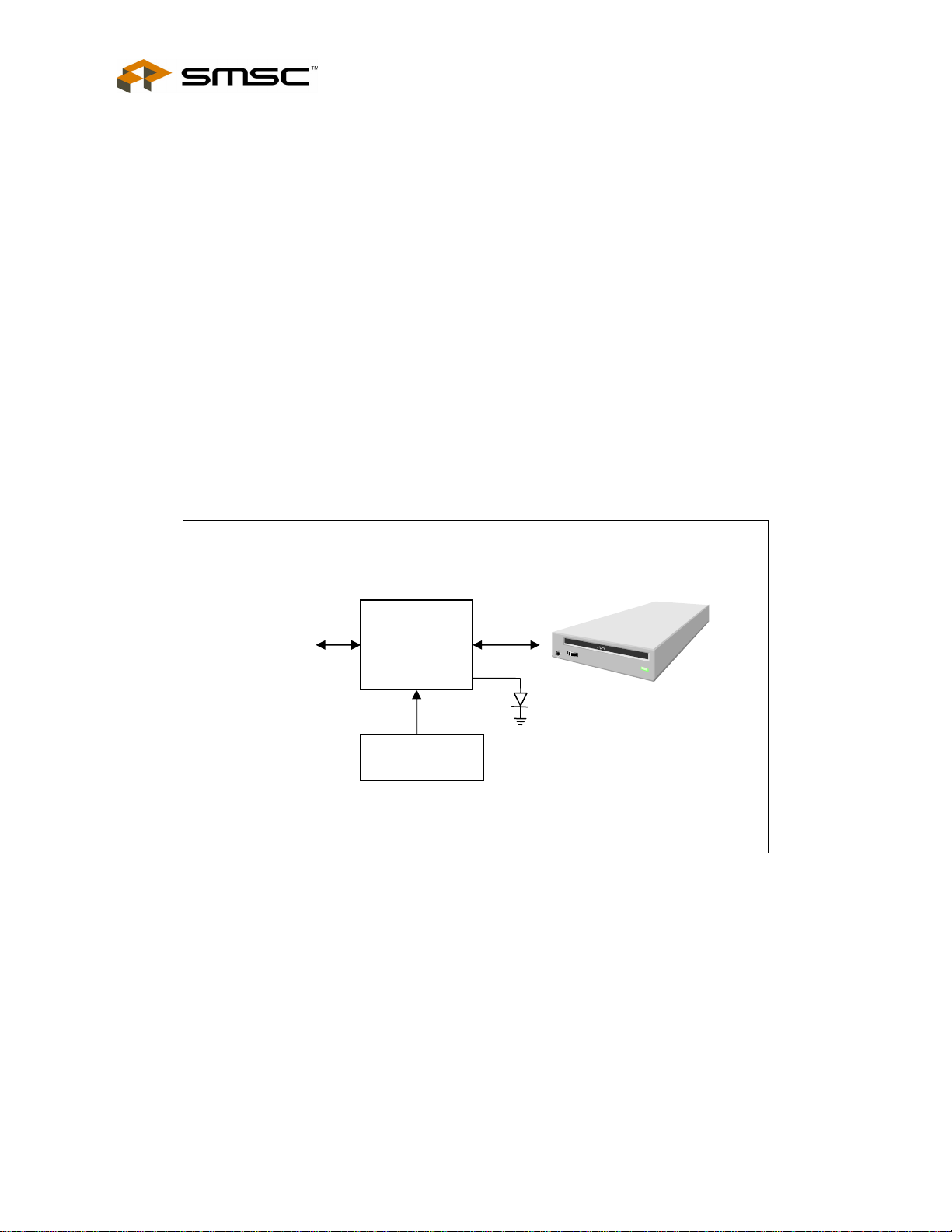
Chapter 1 General Description
The USB97C202 is a USB2.0 Mass Storage Class Peripheral Controller intended for use with standard
ATA-5 and -6 hard drives and standard ATAPI-5 devices.
The device consists of a USB 2.0 PHY and SIE, buffers, Fast 8051 microprocessor with expanded
scratchpad and 768 of program SRAM, internal 48 KB program ROM, and an ATA-66 compatible
interface.
Provisions for optional external Flash Memory up to 64K bytes for program storage is provided. A serial
EEPROM which can be modified via USB from the host provides unique VID/PID/Serial numbers, as well
as optional configuration information.
Internal 768 Bytes of scratchpad SRAM are also provided.. This internal SRAM can also be used for
program storage to implement program upgrade via USB download to external “boot block” Flash program
memory, if desired.
Seven GPIO pins are provided for controlling external power control elements and sensing specialized
drive functions. Provisions are made to allow dynamic attach and re-attach to the USB bus to allow hot
swap of drives to be implemented.
USB 2.0 ATA/ATAPI Controller
Datasheet
ATA-6 HDD or
ATAPI-5 Optical drive
USB2.0
BUS
USB97C202
Serial EEPROM
(VID/PID/options)
ATA-66
HS Indicator
SMSC USB97C202 Page 4 Revision 1.2 (02-04-04)
DATASHEET
USB 2.0 ATA/ATAPI Controller
Datasheet
Chapter 2 Pin Table
DISK DRIVE INTERFACE (27 Pins)
IDE_D0 IDE_D1 IDE_D2 IDE_D3
IDE_D4 IDE_D5 IDE_D6 IDE_D7
IDE_D8 IDE_D9 IDE_D10 IDE_D11
IDE_D12 IDE_D13 IDE_D14 IDE_D15
IDE_nIOR IDE_nIOW IDE_IRQ IDE_DACK
IDE_DRQ IDE_nCS0 IDE_nCS1 IDE_SA0
IDE_SA1 IDE_SA2 IORDY
USB INTERFACE (7 Pins)
USBD+ USBD- LOOPFLTR RBIAS
RTERM FS+ FS-
MEMORY/IO INTERFACE (28 Pins)
MD0 MD1 MD2 MD3
MD4 MD5 MD6 MD7
MA0 MA1 MA2 MA3
MA4 MA5 MA6 MA7
MA8 MA9 MA10 MA11
MA12 MA13 MA14 MA15
nMRD nIOR nMWR nIOW
ROMEN GPIO1/HS GPIO2/EE_CS GPIO3/VBUS
GPIO4/EE_DIO GPIO5/ATA RESET GPIO6/A16 GPIO7/EE_CLK
XTAL1/CLKIN XTAL2 nRESET nTEST/nDBGSTR
TST_OUT/DBGOUT nTESTEN CLKOUT
POWER, GROUNDS, and NO CONNECTS (23 Pins)
MISC (15 Pins)
SMSC USB97C202 Page 5 Revision 1.2 (02-04-04)
DATASHEET
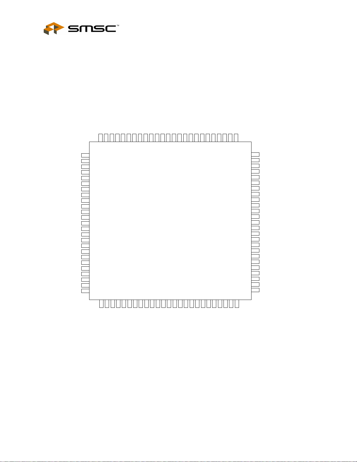
Chapter 3 Pin Configuration
ROMEN
GPIO1
GPIO2
GPIO3
GND
GPIO4
GPIO5
GPIO6
GPIO7
nTEST0
nTEST1
nTEST2
VDDIO
IDE_D8
IDE_D7
IDE_D9
VDD
IDE_D6
IDE_D10
GND
IDE_D5
USB 2.0 ATA/ATAPI Controller
Datasheet
IDE_D11
IDE_D4
VDDIO
IDE_D12
RBIAS
VDDA
FS+
USB+
USB-
FS-
RTERM
VSSA
XTAL1/CLKIN
XTAL2
VSSP
LOOPFLTR
VDDP
N.C.
N.C.
MD7
MD6
MD5
MD4
GND
MD3
MD2
MD1
MD0
nRESET
75
51
IDE_D3
IDE_D13
IDE_D2
GND
IDE_D14
IDE_D1
IDE_D15
IDE_D0
VDDIO
IDE_DRQ
IDE_nIOW
IDE_nIOR
USB97C202
1
25
IORDY
GND
IDE_DACK
IDE_IRQ
IDE_SA1
IDE_SA0
VDD
IDE_SA2
IDE_nCS0
IDE_nCS1
VDDIO
nMWR
nMRD
nIOR
nIOW
MA9
MA8
VDD
GND
MA15
MA14
MA13
MA12
MA11
VDDIO
CLKOUT
MA10
MA7
VDDIO
N.C.
MA6
MA5
MA4
MA3
MA2
MA1
MA0
GND
Figure 3.1 – 100 PIN STQFP
SMSC USB97C202 Page 6 Revision 1.2 (02-04-04)
DATASHEET

SRAM
1.25KB
512 Bytes EP2 TX/RX Buffer B
ROMEN
Drive
ATA/ATAPI
48KB ROM
Clocked byPhase 2 Cloc k
ATA-66
Interface
Future phase 3
15MHz
Data @ 32 bit
GPIO 7 pins
SRAM
768 Byte
Program/Scratchp ad
Bus
Program Memory/ IO
2 pins
MEM/IO Bus 29pins
Debug
Serial 2 wire ( Data/Strobe)
Clocked byPhase 1 Clock
60MHz32 Bit
8 bits ( Address and Data bus ses )
s
s
u
B
a
t
a
D
64 Bytes EP0TX
64 Bytes EP1TX
64 Bytes EP0RX
64 Bytes EP1RX
512 Bytes EP2 TX/RX Buffer A
Latch phase 1 Latch phase 2
Address Register
XDATA
CPU CORE
Interrupt Controller
FAST 8051
DATASHEET
USB 2.0 ATA/ATAPI Controller
Datasheet
Chapter 4 Block Diagram
Latch phase 0
Address
Osc
Address MUX
s
s
s
s
e
e
r
r
d
d
d
d
A
A
Address
Address
EP1TX_BC
EP0TX_BC
EP0RX_BC
Auto address generators
EP1RX_BC
Address
Address
Clocked byPhase 0 Clock
RAMRD_A/B
RAMWR_A/B
SIE Control Regs
32 bit 15MHz Data Buss
SIE
( Serial Interface Engine )
Clock Generation
Configuration and Control
USB 2.0 PHY
( Transciever )
XTAL
12 MHz
CLOCKOUT
7 pins
OPTIONAL
External PHY
SMSC USB97C202 Page 7 Revision 1.2 (02-04-04)

Chapter 5 Pin Descriptions
Table 5.1 – USB97C202 Pin Descriptions
DISK DRIVE INTERFACE
IDE DMA
Request
IDE IO Read
Strobe
IDE Register
Address 1
IDE Register
Address 0
IDE Register
Address 2
IDE Data IDE_D15 IO20 This pin is the bi-directional data bus bit 15
IDE IO Write
Strobe
IDE DMA
Acknowledge
IDE Interrupt
Request
IDE Data IDE_D13 IO20 This pin is the bi-directional data bus bit 13
IDE Data IDE_D14 IO20 This pin is the bi-directional data bus bit 14
IDE Chip
Select 0
IDE Chip
Select 1 0
IDE Data IDE_D[0:12] IO20 These pins are bits 0-12 of the ATA/ATAPI bi-
IO Ready IORDY I This pin is the active high IORDY signal from
IDE_DRQ IS This pin is the active high DMA request from
the ATA/ATAPI interface.
IDE_nIOR O20 This pin is the active low read signal for the
interface.
IDE_SA1 O20 This pin is the register select address bit 1
signal for the ATA/ATAPI interface.
IDE_SA0 O20 This pin is the register select address bit 0
signal for the ATA/ATAPI interface.
IDE_SA2 O20 This pin is the register select address bit 2
signal for the ATA/ATAPI interface.
signal for the ATA/ATAPI interface.
IDE_nIOW O20 This pin is active low write signal for the
ATA/ATAPI interface.
IDE_nDACK O20 This pin is the active low DMA acknowledge
signal for the ATA/ATAPI interface.
IDE_IRQ IS This pin is the active high interrupt request
signal for the ATA/ATAPI interface.
signal for the ATA/ATAPI interface.
signal for the ATA/ATAPI interface.
.
IDE_nCS0 O20 This pin is the active low chip select 0 signal for
the ATA/ATAPI interface.
IDE_nCS1 O20 This pin is the active low select 1 signal for the
ATA/ATAPI interface.
directional data bus.
the IDE drive.
USB 2.0 ATA/ATAPI Controller
Datasheet
SMSC USB97C202 Page 8 Revision 1.2 (02-04-04)
DATASHEET

USB 2.0 ATA/ATAPI Controller
Datasheet
USB Bus
Data
USB
Transceiver
Filter
USB
Transceiver
Bias
Termination
Resistor
Full Speed
USB Data
Memory Data
Bus
Memory
Address Bus
Memory Write
Strobe
Memory Read
Strobe
IO Read
Strobe
IO Write
Strobe
Crystal
Input/External
Clock Input
Crystal Output XTAL2 OCLKx 12Mhz Crystal
Clock Output CLKOUT O8 This pin produces a 30Mhz clock signal
Internal ROM
Enable
USB INTERFACE
USBUSB+
IO-U These pins connect to the USB bus data
signals.
LOOPFLTR This pin provides the ability to supplement the
internal filtering of the transceiver with an
external network, if required.
RBIAS A 9.09 Kohm precision resistor is attached
from ground to this pin to set the transceiver’s
internal bias currents.
RTERM A precision 1.5Kohm precision resistor is
attached to this pin from a 3.3V supply.
FSFS+
IO-U These pins connect to the USB- and USB+
pins through 31.6 ohm series resistors.
MEMORY/IO INTERFACE
MD[7:0] IO12PU When ROMEN=0, these signals are used to
transfer data between the internal CPU and the
external program memory. When ROMEN=1, a
weak internal pull up is activated to prevent
these pins from floating.
MA[15:0] O12 These signals address memory locations within
the external memory.
nMWR O12 Program Memory Write; active low
nMRD O12 Program Memory Read; active low
nIOR O12 XDATA space Read; active low
nIOW O12 XDATA space Write; active low
MISC
XTAL1/
CLKIN
ICLKx 12Mhz Crystal or external clock input.
This pin can be connected to one terminal of
the crystal or can be connected to an external
12Mhz clock when a crystal is not used.
This is the other terminal of the crystal, or left
open when an external clock source is used to
drive XTAL1/CLKIN. It may not be used to
drive any external circuitry other than the
crystal circuit.
independent of the processor clock divider. It is
held inactive and low whenever the internal
processor clock is stopped or is being obtained
from the ring oscillator.
ROMEN IP When left unconnected or tied high, the
USB97C202 uses the internal ROM for
program execution. When tied low, an external
program memory should be connected to the
memory/data bus. The state of this pin latched
internally on the rising edge of nRESET.
SMSC USB97C202 Page 9 Revision 1.2 (02-04-04)
DATASHEET

USB 2.0 ATA/ATAPI Controller
MISC
General
Purpose I/O
GPIO[1:7] IO20 These general purpose pins may be used
either as inputs, edge sensitive interrupt inputs,
or outputs. When using internal ROM mode,
these pins have the following assignments:
GPIO1: USB HS Indicator; active high
GPIO2: Serial EEPROM (93LC66 type) Chip
Select
GPIO3: USB VBUS Detect Input
GPIO4: Serial EEPROM Data In/Out
GPIO5: ATA Drive Reset
GPIO6: A16 control line for external program
Flash memory when using firmware upgrade
capability (external ROM operation only)
GPIO7: Serial EEPROM Clock output
RESET input nRESET IS This active low signal is used by the system to
reset the chip. The active low pulse should be
at least 100ns wide.
Test input nTest[0:2] IP These signals are used for testing the chip.
User should normally leave them unconnected.
For board testing, all pads except these test
inputs are included in an XNOR chain, such
that by tying nTEST2 low, nIOR will reflect the
toggling of a signal on each pin. Circuit board
continuity of the pin solder connections after
assembly can be checked in this manner
POWER, GROUNDS, and NO CONNECTS
VDD +2.5V Core power
VDDIO +3.3V I/O power
VDDP +2.5 Analog power
VSSP Analog Ground Reference
VDDA +3.3V Analog power
VSSA Analog Ground Reference
GND Ground Reference
NC No Connect. These pins should not be
connected externally.
Datasheet
SMSC USB97C202 Page 10 Revision 1.2 (02-04-04)
DATASHEET

USB 2.0 ATA/ATAPI Controller
Datasheet
5.1 Buffer Type Descriptions
Table 5.2 - USB97C202 Buffer Type Descriptions
BUFFER DESCRIPTION
I Input
IS Input with Schmitt trigger
IP Input with weak pull-up
IO8 Input/Output with 8 mA drive
O8 Output with 8mA drive
O12 Output with 12mA drive
IO12PU Input/Output with 12 ma drive and
controlled weak pull up
IO12 Input/Output with 12 ma drive
IO20 Input/output with 20mA drive
O20 Output with 20mA drive
O20PU Output with 20mA drive and weak pullup
ICLKx XTAL clock input
OCLKx XTAL clock output
I/O-U Defined in USB specification
SMSC USB97C202 Page 11 Revision 1.2 (02-04-04)
DATASHEET

Datasheet
A
of
C17
.1uF
C16
.1uF
11Friday, June 07, 2002
USB 2.0 ATA/ATAPI Controller
IDE_D[0:15]
C15
.1uF
VR1
VCCEXT
12
VDDIO,VDDA
VDDIO
C12
10uF
+
GND
VIN VOUT
3 2
C11
10uF
+
R15
1%
9.09K
1/10W
IDE_nIOW
C14
.1uF
C13
.1uF
VDD
C19
1
VDDIO
R16
1.5K1/10W
USB+
FS-
USB-
VDDA
FS+
IDE_nCS1
IDE_nCS0
IDE_SA2
IDE_SA0
IDE_nIOR
IDE_DACK
10uF
+
GND
1
2.5V Regulator
VIN VOUT
VR2
3 2
5%
C18
10uF
+
VCCEXT
MA13
MA12
U1
9
867
593
VDDVDDIO
MA12
MA13
RTERMN.C .
8289
MA14
MA14
MA15
5
MA15
USB+
79
FS-
81
USB-
80
RBIAS
76
87
VDDA
77
FS+
78
GND
47
40
30
29
GND
37
IDE_SA0
33
IDE_SA2
31
39
36
IDE_SA1
34
IDE_D13
49
IDE_IRQ
35
IDE_D14
46
41
IDE_D15
44
IDE_D12
IDE_D11
5154565760526261585553835048454342387574737270
VDDIO
IDE_D11
VDD
IDE_DRQ
IDE_IRQ
IDE_D12
IDE_D14
IDE_SA1
IDE_D13
IDE_D15
MA2
MA0
MA1
1211109876527262325428292224311
A0A1A2A3A4A5A6A7A8
D0D1D2D3D4D5D6
13141517181920
MA[0:15]
MA7
MA8
MA6
MA5
MA9
MA3
MA11
MA10
MA4
161718192195222324329998979694
12
111314
15
MA7
MA6
MA5
MA4
MA9
MA8
GND
MA10
MA11
VDDIO
LOOPFLTR
IDE_nIOW
IDE_nC S0
IDE_nC S1
IDE_nIOR
IDE_DACK
USB9 7C20 2
IDE_DRQ
GND
IDE_D10
IDE_D9
VDDIO
IDE_D8
IDE_D7
IDE_D6
IDE_D5
IDE_D4
VSSA
IDE_D6
IDE_D8
IDE_D5
IDE_D4
IDE_D3
IDE_D7
IDE_D10
IDE_D9
MA3
MA6
MA5
MA4
MA9
MA7
MA8
A9
D7
21
MA1
MA2
MA0
MA3
MA2
MA1
MA0
MD0
MD1
VDD
GND
IDE_D3
IDE_D2
IDE_D1
IDE_D0
VDDIO
IORDY
ROMEN
GPIO1
IDE_D0
IORDY
IDE_D2
IDE_D1
VDDIO
39VF512-70 or equi v OTP/EPROM
R17
OPTIONAL for test purposes only, if used tie ROMEN
12.00Mhz
R3
120
USB97C202 Typical Application
C
Title
Size Document Number Rev
Date: Sheet
low;otherwise do not populate
10K
C20 1µf
C22
22pf
DATASHEET
C21
22pf
LED
D1
MA12
MA13
MA10
MA14
MA15
MA11
3
OE
CE
WE
A15
A10
A11
A12
A13
A14
VPP
VCC
GNDNCNC
32
16230
U2
VDDIO
88
MD2
MD3
MD4
VDDP
MD5
93
MD6
92
MD7
91
N.C.
20
VDDIO
28
nMRD
26
GND
25
nMWR
27
nIOW
2
nIOR
1
nTEST2
64
nRESET
100
VDD
10
CLKOUT
4
VSSP
XTAL2
XTAL1/ CL KI N
nTEST1
nTEST0
GND
GPIO7
GPIO6
VDDIO
GPIO5
N.C.
GPIO2
GPIO3
GPIO4
90
GPIO3
GPIO2
U3
86
85
84
65
66
71
67
68
63
69
nRESET
123
CS
VCC
Y1
Q1
R18
1K
45
DI
DOVSS
CLK
N.C.
N.C.
93LC66A Serial EEPROM
678
VCCD+D-
GND
P2
USB TYPE B
132
R13
IDE_nCS1
IDE_SA2
DVDD
12
36384039
35
12
12
37
12
R6
2.21K
1/8W
1%
C1
0.047uF
25V
10%
IDE supports :
Mode1, Mode2, Mode 3, Mode4
Ultra DMA 33/66
IDE_D14
IDE_D8
IDE_D13
IDE_D9
IDE_D15
IDE_D12
IDE_D10
IDE_D11
10
12
1615
22242628303234
P1
1
3 425 6
7 8
9
11
13 14
17 18
19 20
21232527293133
GPIO3
T1 GREEN
LED1
R9
332
1/8W
1%
12
R8
4.75K
1/8W
1%
4
10K
USB+
USB-
R14
1M
3.3V Regulator
R1131.6
R1231.6
1 2
1 2
FS-
FS+
Prim ary IDE
IDE_D0
IDE_D6
IDE_D2
IDE_D4
IDE_D1
IDE_D3
IDE_D5
IDE_D7
12
R2
5.62K
1/8W
1%
R1 100
1/8W 1%
nRESET
IDE_D7
IDE_D6
IDE_D9
IDE_D8
IDE_nIOW
IDE_nIOR
IDE_DRQ
IORDY
IDE_D3
IDE_D11
IDE_D5
IDE_D10
IDE_D12
IDE_D4
R7
1.0K
1/8W
1%
DVDD
12
R7
1.0K
1/8W
1%
DVDD
12
IDE_IRQ
IDE_SA1
IDE_nCS0
IDE_SA0
IDE_DACK
C10
.1uF
DVDD
C9
.1uF
C8
.1uF
VCCEXT
C7
.1uF
C6
.1uF
C5
.1uF
C4
IDE_D0
IDE_D15
IDE_D14
IDE_D1
IDE_D2
IDE_D13
.1uF
VDD
C3
.1uF
Chapter 6 Typical Application
C2
.1uF
SMSC USB97C202 Page 12 Revision 1.2 (02-04-04)

USB 2.0 ATA/ATAPI Controller
Datasheet
Chapter 7 DC Parameters
7.1 Maximum Guaranteed Ratings
Operating Temperature Range........................................................................................................................... 0
Storage Temperature Range ............................................................................................................................-55
Lead Temperature Range (soldering, 10 seconds) ..................................................................................................... +325
o
C to +70oC
o
to +150oC
o
C
Positive Voltage on any pin, with respect to Ground ........................................................................................................5.5V
Negative Voltage on any pin, with respect to Ground......................................................................................................-0.3V
Maximum V
Maximum V
DDA, VDDIO
DD, VDDP
......................................................................................................................................................+4.0V
.........................................................................................................................................................+3.0V
*Stresses above the specified parameters could cause permanent damage to the device. This is a stress rating only and
functional operation of the device at any other condition above those indicated in the operation sections of this
specification is not implied.
Note: When powering this device from laboratory or system power supplies, it is important that the Absolute
Maximum Ratings not be exceeded or device failure can result. Some power supplies exhibit voltage
spikes on their outputs when the AC power is switched on or off. In addition, voltage transients on the AC
power line may appear on the DC output. When this possibility exists, it is suggested that a clamp circuit
be used.
Table 7.1 - DC Electrical Characteristics
(T
= 0°C - 70°C, V
A
DDIO, VDDA
= +3.3 V ± 10%, V
DD, VDDP
= +2.5 V ± 10%,)
PARAMETER SYMBOL MIN TYP MAX UNITS COMMENTS
I Type Input Buffer
Low Input Level
High Input Level
ICLK Input Buffer
Low Input Level
High Input Level
Input Leakage
(All I and IS buffers)
Low Input Leakage
High Input Leakage
V
ILI
V
IHI
V
ILCK
V
IHCK
I
IL
IIH
2.0
2.2
-10
-10
0.8
0.4
+10
+10
V
V
V
V
uA
uA
TTL Levels
VIN = 0
VIN = V
DDIO
SMSC USB97C202 Page 13 Revision 1.2 (02-04-04)
DATASHEET

PARAMETER SYMBOL MIN TYP MAX UNITS COMMENTS
O8 Type Buffer
Low Output Level
High Output Level
Output Leakage
I/O8 Type Buffer
Low Output Level
High Output Level
Output Leakage
I/O12 Type Buffer
Low Output Level
High Output Level
Output Leakage
I/O20 Type Buffer
Low Output Level
High Output Level
Output Leakage
USB 2.0 ATA/ATAPI Controller
V
OL
VOH
IOL
2.4
-10
0.4
+10
V
V
uA
IOL = 8 mA @ V
= 3.3V
I
= -4mA @ V
OH
= 3.3V
V
= 0 to V
IN
Datasheet
DDIO
DDIO
DDIO
(Note 7.1)
V
OL
VOH
IOL
2.4
-10
0.4
+10
V
V
µA
IOL = 8 mA @ V
= 3.3V
I
= -4 mA @ V
OH
= 3.3V
V
= 0 to V
IN
DDIO
DDIO
DDIO
(Note 7.1, Note 7.3)
V
OL
VOH
I
OL
V
OL
V
OH
IOL
2.4
-10
2.4
-10
0.4
+10
0.4
+10
V
I
= 12 mA @ V
OL
= 3.3V
I
= -6mA @ V
OH
V
= 3.3V
V
= 0 to V
µA
IN
(Note 7.1, Note 7.3)
V
V
µA
= 20 mA @ V
I
OL
= 3.3V
I
= -5 mA @ V
OH
= 3.3V
V
= 0 to V
IN
DDIO
DDIO
DDIO
DDIO
DDIO
DDIO
(Note 7.1, Note 7.3)
SMSC USB97C202 Page 14 Revision 1.2 (02-04-04)
DATASHEET

USB 2.0 ATA/ATAPI Controller
Datasheet
PARAMETER SYMBOL MIN TYP MAX UNITS COMMENTS
IO-U
Note 7.2
Supply Current Unconfigured I
Supply Current Active ICC 85
65
CCINIT
85
mA
mA
mA
120
mA
Note 7.1 Output leakage is measured with the current pins in high impedance.
Note 7.2 See appendix A for USB DC electrical characteristics.
Note 7.3 Output leakage is valid only on pins without internal weak pull ups or pull downs.
7.1.1 Capacitance TA = 25°C; FC = 1MHz; VDD = 2.5V
LIMITS
PARAMETER SYMBOL MIN TYP MAX UNIT TEST CONDITION
Clock Input Capacitance CIN 20 pF
Input Capacitance CIN 10 pF
Output Capacitance C
20 pF
OUT
V
DDIO, VDDA
V
DD, VDDP
V
DDIO, VDDA
V
DD, VDDP
All pins except USB pins
(and pins under test tied
to AC ground)
SMSC USB97C202 Page 15 Revision 1.2 (02-04-04)
DATASHEET

Chapter 8 AC Specifications
8.1 ATA/ATAPI
The USB97C202 conforms to all timing diagrams and specifications for ATAPI-5 as set forth in the
T13/1321D Revision 3 NCITS specification. Please refer to this specification for more information.
8.2 USB2.0 Timing
The USB97C202 conforms to all timing diagrams and specifications for USB peripheral silicon building
blocks as set forth in the USB-IF USB 2.0 specification. Please refer to this specification for more
information.
USB 2.0 ATA/ATAPI Controller
Datasheet
SMSC USB97C202 Page 16 Revision 1.2 (02-04-04)
DATASHEET

USB 2.0 ATA/ATAPI Controller
A
g
y
y
y
g
g
y
Datasheet
Chapter 9 Package Outline
Figure 9.1 - 100 Pin STQFP Package Outline, 12x12x1.4 Body, 2MM Footprint (Rev A)
Table 9.1 – 100 Pin STQFP Package Parameters (Rev A)
MIN NOMINAL MAX REMARKS
A1
A2
D
D1
E
E1
H
L
L1
e
θ
W
R1
R2
ccc
Notes:
1
Controlling Unit: millimeter.
2
Tolerance on the true position of the leads is ± 0.035 mm maximum.
3
Package body dimensions D1 and E1 do not include the mold protrusion.
Maximum mold protrusion is 0.25 mm.
4
Dimension for foot length L measured at the gauge plane 0.25 mm above the seating plane.
5
Details of pin 1 identifier are optional but must be located within the zone indicated.
~ ~ 1.60 Overall Packa
0.05 ~ 0.15 Standoff
1.35 ~ 1.45 Bod
Thickness
13.80 ~ 14.20 X Span
11.80 ~ 12.20 X bod
13.80 ~ 14.20 Y Span
11.80 ~ 12.20 Y bod
0.09 ~ 0.20 Lead Frame Thickness
0.45 0.60 0.75 Lead Foot Len
~ 1.00 ~ Lead Len
o
~ 7
0
0.40 Basic Lead Pitch
o
Lead Foot Angle
0.13 0.16 0.23 Lead Width
0.08 ~ ~ Lead Shoulder Radius
0.08 ~ 0.20 Lead Foot Radius
~ ~ 0.08 Coplanarit
e Height
Size
Size
th
th
SMSC USB97C202 Page 17 Revision 1.2 (02-04-04)
DATASHEET
 Loading...