


查询USB97C100QFP供应商
Multi-Endpoint USB Peripheral Controller
USB97C100
ADVANCE INFORMATION
FEATURES
High Performance USB Peripheral Controller
Engine
- Integrated USB Transceiver
- Serial Interface Engine (SIE)
- 8051 Microcontroller (MCU)
- Patented Memory Management Unit (MMU)
- 4 Channel 8237 DMA Controller
(ISADMA)
- 4K Byte On Board USB Packet Buffer
- Quasi-ISA Peripheral Interface
- USB Bus Snooping Capabilities
-GPIOs
Complete USB Specification 1.1 Compatibility
- Isochronous, Bulk, Interrupt, and Control
Data Independently Configurable per
Endpoint
- Dynamic Hardware Allocation of -Packet
Buffer for Virtual Endpoints
- Multiple Virtual Endpoints (up to 16 TX, 16
RX Simultaneously)
- Multiple Alternate Address Filters
- Dynamic Endpoint Buffer Length
Allocation (0-1280 Byte Packets)
High Speed (12Mbps) Capability
MMU and SRAM Buffer Allow Buffer Optimization
and Maximum Utilization of USB Bandwidth
- 128 Byte Page Size
- 10 Pages Maximum per Packet
- Up to 16 Deep Receive Packet Queue
- Up to 5 Deep Transmit Packet Queue, per
Endpoint
- Hardware Generated Packet Header
Records Each Packet Status Automatically
- Simultaneous Arbitration Between MCU,
SIE, and ISA DMA Accesses
Extended Power Management
- Standard 8051 "Stop Clock" Modes
- Additional USB and ISA Suspend
Resume Events
- Internal 8MHz Ring Oscillator for Immediate
Low Power Code Execution
- 24, 16, 12, 8, 4, and 2 MHz PLL Taps For on
the Fly MCU and DMA Clock Switching
- Independent Clock/Power Management for
SIE, MMU, DMA and MCU
DMA Capability with ISA Memory
- Four Independent Channels
- Transfer Between Internal and External
Memory
- Transfer Between I/O and Buffer Memory
- External Bus Master Capable
External MCU Memory Interface
- 1M Byte Code and Data Storage via 16K
Windows
- Flash, SRAM, or EPROM
- Downloadable via USB, Serial Port, or ISA
Peripheral
Quasi-ISA Interface Allows Interface to New and
"Legacy" Peripheral Devices
- 1M ISA Memory Space via 4K MCU Window
- 64K ISA I/O Space via 256 Byte MCU
Window
- 4 External Interrupt Inputs
- 4 DMA Channels
- Variable Cycle Timing
- 8 Bit Data Path
5V or 3.3v Operation
On Board Crystal Driver Circuit
128 Pin QFP Package
ORDERING INFORMATION
Order Number: USB97C100QFP
128 Pin QFP Package
SMSC DS – USB97C100 Rev. 01/03/2001

GENERAL DESCRIPTION
The USB97C100 is a flexible, general purpose USB peripheral interface and controller ideally suited for multiple
endpoint applications. The USB97C100 provides an ISA-like bus interface, which will allow virtually any PC peripheral to
be placed at the end of a USB connection. Its unique dynamic buffer architecture overcomes the throughput
disadvantages of existing fixed FIFO buffer schemes allowing maximum utilization of the USB connection’s overall
bandwidth. This architecture minimizes the integrated microcontroller’s participation in the USB data flow, allowing backto-back packet transfers to block oriented devices. The efficiency of this architecture allows floppy drives to coexist with
other peripherals such as serial and parallel ports on a single USB link.
The USB97C100 allows external program code to be downloaded over the USB to allow easy implementation of varied
peripheral USB Device Classes and combinations. This also provides a method for convenient field upgrades and
modifications.
© STANDARD MICROSYSTEMS CORPORATION (SMSC) 2001
80 Arkay Drive
Hauppauge, NY 11788
(631) 435-6000
FAX (631) 273-3123
Standard Microsystems is a registered trademark of Standard Microsystems Corporation, and SMSC is a trademark of Standard Microsystems
Corporation. Product names and company names are the trademarks of their respective holders. Circuit diagrams utilizing S MSC products are incl uded
as a means of illustrating typical applications; consequently complete information sufficient for construction purposes is not necessarily given. Although
the information has been checked and is believed to be accurate, no responsibility is assumed for inaccuracies. SMSC reserves the right to make
changes to specifications and product descriptions at any time without notice. Contact your local SMSC sales office to obtain the latest speci fications
before placing your product order. The provision of this information does not convey to the purchaser of the semiconductor devices described any
licenses under the patent rights of SMSC or others. All sales are expressly conditional on your agreement to the terms and conditions of the most
recently dated version of SMSC's standard Terms of Sale Agreement dated before the date of your order (the "Terms of Sale Agreem ent" ). T he product
may contain design defects or errors known as anomalies which may cause the product's functions to deviate from published specifications. Anom aly
sheets are available upon request. SMSC products are not designed, intended, authorized or warranted for use in any life support or other application
where product failure could cause or contribute to personal injury or severe property damage. Any and all such uses without prior written approval of an
Officer of SMSC and further testing and/or modification will be fully at the risk of the customer. Copies of this document or other SMSC literature, as well
as the Terms of Sale Agreement, may be obtained by visiting SMSC’s website at http://www.smsc.com.
SMSC DISCLAIMS AND EXCLUDES ANY AND ALL WARRANTIES, INCLUDING WITHOUT LIMITATION ANY AND ALL IMPLIED WARRANTIES
OF MERCHANTABILITY, FITNESS FOR A PARTICULAR PURPOSE, TITLE, AND AGAINST INFRINGEMENT, AND ANY AND ALL WARRANTIES
ARISING FROM ANY COURSE OF DEALING OR USAGE OF TRADE.
IN NO EVENT SHALL SMSC BE LIABLE FOR ANY DIRECT, INCIDENTAL, INDIRECT, SPECIAL, PUNITIVE, OR CONSEQUENTIAL DAMAGES,
OR FOR LOST DATA, PROFITS, SAVINGS OR REVENUES OF ANY KIND; REGARDLESS OF THE FORM OF ACTION, WHETHER BASED ON
CONTRACT, TORT, NEGLIGENCE OF SMSC OR OTHERS, STRICT LIABILITY, BREACH OF WARRANTY, OR OTHERWISE; WHETHER OR NOT
ANY REMEDY IS HELD TO HAVE FAILED OF ITS ESSENTIAL PURPOSE; AND WHETHER OR NOT SMSC HAS BEEN ADVISED OF THE
POSSIBILITY OF SUCH DAMAGES.
SMSC DS – USB97C100 Page 2 Rev. 01/03/2001

TABL E O F CONTENTS
FEATURES................................................................................................................................................................... 1
GENERAL DESCRIPTION............................................................................................................................................ 2
PIN CONFIGURATION................................................................................................................................................. 4
DESCRIPTION OF PIN FUNCTIONS........................................................................................................................... 5
BUFFER TYPE DESCRIPTIONS.................................................................................................................................. 7
FUNCTIONAL DESCRIPTION...................................................................................................................................... 9
Serial Interface Engine (SIE)......................................................................................................................................... 9
Micro Controller Unit (MCU).......................................................................................................................................... 9
SIEDMA......................................................................................................................................................................... 9
Memory Management Unit (MMU) Register Description............................................................................................... 9
ISADMA......................................................................................................................................................................... 9
Applications................................................................................................................................................................. 10
TYPICAL SIGNAL CONNECTIONS............................................................................................................................ 12
MCU MEMORY MAP.................................................................................................................................................. 13
Code Space................................................................................................................................................................. 13
Data Space.................................................................................................................................................................. 13
ISADMA Memory Map................................................................................................................................................. 13
MCU Block Register Summary.................................................................................................................................... 14
MMU Block Register Summary................................................................................................................................... 15
SIE Block Register Summary...................................................................................................................................... 16
MCU REGISTER DESCRIPTION................................................................................................................................ 17
MCU Runtime Registers.............................................................................................................................................. 17
FIFO Status Registers................................................................................................................................................. 20
MCU Power Management Registers...........................................................................................................................24
MCU ISA Interface Registers...................................................................................................................................... 27
8237 (ISADMA) REGISTER DESCRIPTION.............................................................................................................. 30
Memory Map................................................................................................................................................................30
Runtime Registers....................................................................................................................................................... 31
MEMORY MANAGEMENT UNIT (MMU) REGISTER DESCRIPTION....................................................................... 37
MMU Interface Registers............................................................................................................................................. 37
MMU FREE PAGES REGISTER................................................................................................................................. 40
16 BYTE DEEP TX COMPLETION FIFO REGISTER................................................................................................ 40
TX FIFO POP REGISTER........................................................................................................................................... 41
SERIAL INTERFACE ENGINE (SIE) REGISTER DESCRIPTION ............................................................................. 45
Packet Header Definition............................................................................................................................................. 45
SIE Interface Registers ............................................................................................................................................... 46
DC PARAMETERS..................................................................................................................................................... 51
USB PARAMETERS................................................................................................................................................... 53
USB DC PARAMETERS............................................................................................................................................. 53
USB AC PARAMETERS.............................................................................................................................................. 54
MECHANICAL OUTLINE............................................................................................................................................ 63
USB97C100 REVISIONS............................................................................................................................................ 64
SMSC DS – USB97C100 Page 3 Rev. 01/03/2001
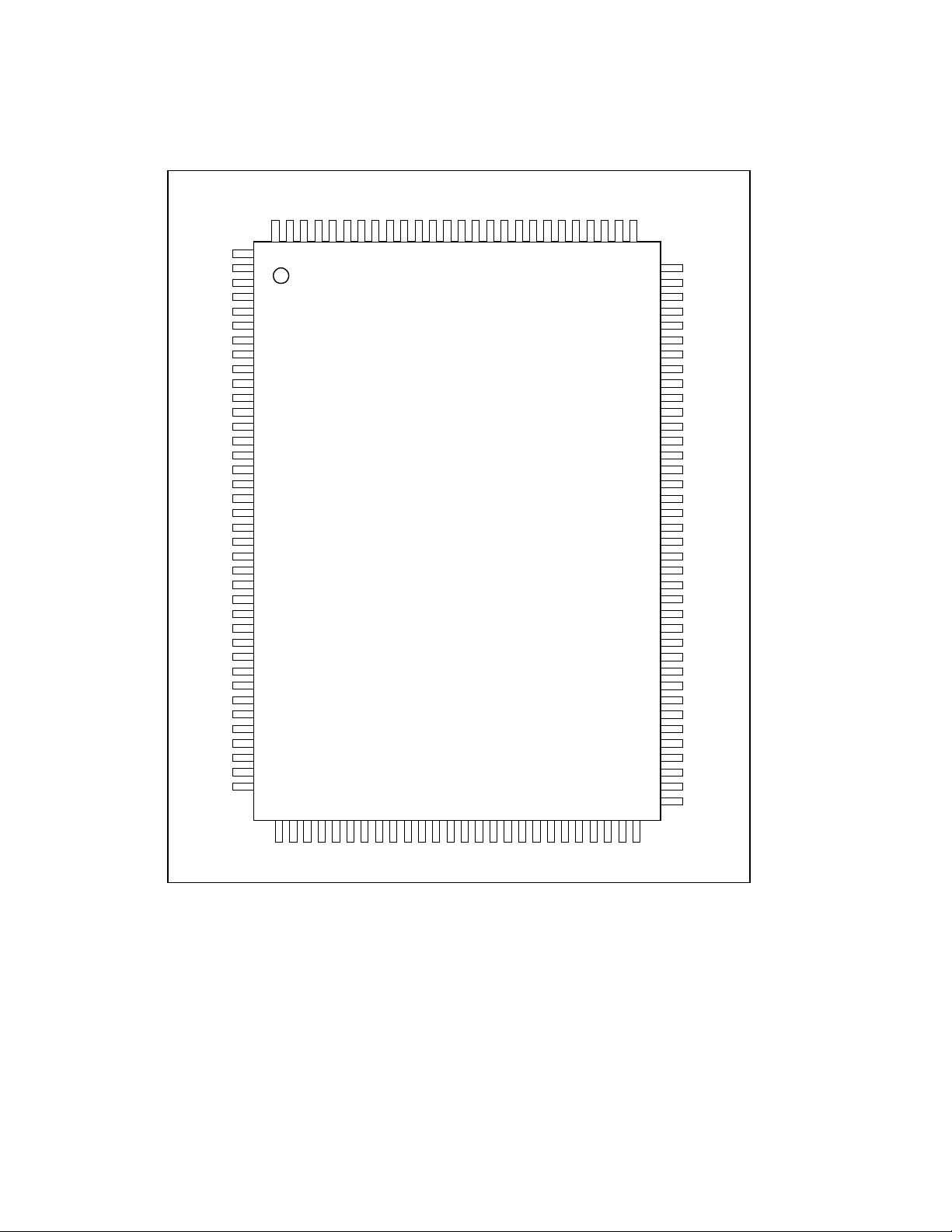
PIN CONFIGURATION
SA11
SA12
nMEMW
nMEMR
nIOR
nIOW
AEN
VCC
SD0
SD1
SD2
SD3
GND
SD4
SD5
SD6
SD7
nDACK0
DRQ0
nDACK1
DRQ1
nDACK2
DRQ2
nDACK3
DRQ3
TC
SA10
SA9
SA8
SA7
SA6
SA5
SA4
GND
SA3
SA2
SA1
SA0
SA13
SA14
SA15
SA16
SA17
SA18
SA19
GND
IRQ3
IRQ2
IRQ1
IRQ0
VCC
nTEST
PWRGD
RESET_IN
TST_OUT
XTAL1
XTAL2
GND
CLKOUT
GPIO0
GPIO1
GPIO2
GPIO3
GPIO4
1
128
127
126
125
124
123
122
121
120
119
118
117
116
115
2
3
4
5
6
7
8
9
10
11
12
13
14
15
16
17
18
19
20
21
22
23
24
25
26
27
28
29
30
31
32
33
34
35
36
37
38
39404142434445464748495051525354555657585960616263
USB97C100
114
113
112
111
110
109
108
107
106
105
104
103
102
101
100
99
98
97
96
95
94
93
92
91
90
89
88
87
86
85
84
83
82
81
80
79
78
77
76
75
74
73
72
71
70
69
68
67
66
65
64
nMASTER
VCC
READY
EXTCLK
FALE
GND
NC
NC
NC
NC
NC
NC
NC
NC
NC
NC
NC
NC
NC
NC
NC
NC
GND
USBD+
VCC3.3
USBDVCC
FA19
FA18
FA11
FA9
FA8
FA13
FA14
FA17
GND
nFWR
FA16
FA0
FA1
FA2
FA3
FA4
FA5
FA6
FD7
FD6
FD5
FD4
FD3
FD2
FD1
FD0
FA10
nFCE
nFRD
GPIO5
GPIO6
GPIO7
GND
VCC
FA7
FA12
FA15
FIGURE 1 - PIN CONFIGURATION
SMSC DS – USB97C100 Page 4 Rev. 01/03/2001

DESCRIPTION OF PIN FUNCTIONS
Table 1 - USB97C100 Pin Configuration
QFP PIN
NUMBER SYMBOL PIN DESCRIPTION
ISA INTERFACE
100 READY Channel is ready when high.
ISA memory or slave devices use this signal to lengthen a bus
cycle from the default time. Extending the length of the bus
cycle can only be done when the bus cycles are derived from
the Internal DMA controller core. 8051 MCU generated Memory
or I/O accesses cannot and will not be extended even if
READY is asserted low by an external ISA slave device. The
external slave device negates this signal after decoding a valid
address and sampling the command signals (nIOW, nIOR,
nMEMW, and nMEMR). When the slave’s access has
completed, this signal should be allowed to float high.
104, 106,
108, 110
105, 107,
109, 111
103 TC DMA Terminal Count; active high.
19-13,
127-7,
9-12
112-115,
117-120
122 AEN Address Enable
123 nIOW I/O Write; active low.
124 nIOR I/O Read; active low.
125 nMEMR Memory read; active low
126 nMEMW Memory write; active low
DRQ[3:0] DMA Request channels 3-0; active high.
These signals are used to request DMA service from the DMA
controller. The requesting device must hold the request signal
until the DMA controller drives the appropriate DMA
acknowledge signal (nDACK[3:0]).
nDACK
[3:0]
DMA Acknowledge channels 3-0; active low.
These signals are used to indicate to the DMA requesting
device that it has been granted the ISA bus.
This signal is used to indicate that a DMA transfer has
completed.
SA[19:0] System Address Bus
These signals address memory or I/O devices on the ISA bus.
SD[7:0] System Data Bus
These signals are used to transfer data between system
devices.
This signal indicates address validation to I/O devices. When
low this signal indicates that an I/O slave may respond to
addresses and I/O commands on the bus. This signal is high
during DMA cycles to prevent I/O slaves from interpreting DMA
cycles as valid I/O cycles.
This signal indicates to the addressed ISA I/O slave to latch
data from the ISA bus.
This signal indicates to the addressed ISA I/O slave to drive
data on the ISA bus.
This signal indicates to the addressed ISA memory slave to
drive data on the ISA bus.
This signal indicates to the addressed ISA memory slave to
latch data from the ISA bus.
BUFFER
TYPE
IP
I
O8
O8
O8
I/O8
O8
O8
O8
O8
O8
SMSC DS – USB97C100 Page 5 Rev. 01/03/2001

QFP PIN
NUMBER SYMBOL PIN DESCRIPTION
102 nMASTER External Bus master, active low
This signal forces the USB97C100 to immediately tri-state its
external bus, even if internal transactions are not complete. All
shared ISA signals are tri-stated, except 8237 nDACKs, which
can be used in gang mode to provide external bus-master
handshaking. This pin must be used with some handshake
mechanism to avoid data corruption.
21-24 IRQ[3:0] Interrupt Request 3-0; active high
These signals are driven by ISA devices on the ISA bus to
interrupt the 8051.
30 XTAL1/
Clock In
24MHz Crystal or clock input.
This pin can be connected to one terminal of the crystal or can
be connected to an external clock when a crystal is not used.
31 XTAL2 24MHz Crystal
This is the other terminal of the crystal.
99 EXTCLK Alternate clock to 8237
An external clock can be used for the internal 8237. This clock
can be used to synchronize the 8237 to other devices.
33 CLKOUT Clock output.
This clock frequency is the same as the 8051 running clock.
This clock is stopped when the 8051 is stopped. Peripherals
should not use this clock when they are expected to run when
the 8051 is stopped. This clock can be used to synchronize
other devices to the 8051.
USB INTERFACE
77, 79 USBD-
USDB+
USB Upstream Connection signals
These are two point-to-point signals and driven differentially.
FLASH INTERFACE
45-52 FD[7:0]
Flash ROM Data Bus
These signals are used to transfer data between 8051 and the
external FLASH.
75, 74, 68,
65, 64, 69,
70, 63, 73,
FA[19:0] Flash ROM Address Bus
These signals address memory locations within the FLASH.
43, 72, 71,
62-58,
56-54
42 nFRD Flash ROM Read; active low O8
66 nFWR Flash ROM Write; active low O8
44 nFCE Flash ROM Chip Select; active low O8
98 FALE Flash ROM address latch enable O8
POWER SIGNALS
25,57,76
VCC +3.3V power or 5V
101,121
78 VCC3.3 +3.3V power for USB
8, 20, 32,
GND Ground Reference
53, 67, 80,
97, 116
MISCELLANEOUS
41-34 GPIO[7:0] General Purpose I/O.
These pins can be configured as inputs or outputs under
software control.
BUFFER
TYPE
IP
I
ICLKx
OCLKx
ICLK
O8
IO-U
IO8
O8
I/O16
SMSC DS – USB97C100 Page 6 Rev. 01/03/2001

QFP PIN
NUMBER SYMBOL PIN DESCRIPTION
27 PWRGD Active high input.
This signal is used to indicate to that chip that a good power
level has been reached. When inactive/low, all pins are Tri-
stated except TST_OUT and a POR is generated.
28 RESET_IN Power on reset; active high
This signal is used by the system to reset the chip. It also
generates an internal POR.
29 TST_OUT AND tree output
This signal is used for testing the chip via an internal AND tree.
26 nTEST Test input
This signal is a manufacturing test pin. User can pull it high or
leave it unconnected.
[96:81] NC No connect
BUFFER TYPE DESCRIPTIONS
Table 2 - USB97C100 Buffer Type Description
BUFFER DESCRIPTION
I Input (no pull-up)
IP Input 90µA with internal pull-up
O8 Output with 8mA drive
I/O8 Input/output with 8mA drive
I/O16 Input/output with 16mA drive
O24 Output, 24mA sink, 12mA source.
I/ODP24 Input/Output drain , 24mA sink, 12mA source with 90µA pull-up
ICLKx XTAL clock input
OCLKx XTAL clock output
ICLK Clock input (TTL levels)
I/O-U Defined in USB specification; uses VCC3.3
BUFFER
TYPE
I
I
O8
IP
Note: These DC Characteristics/drive strengths apply to 5V operation only. See the DC Characteristics section for
additional details.
SMSC DS – USB97C100 Page 7 Rev. 01/03/2001
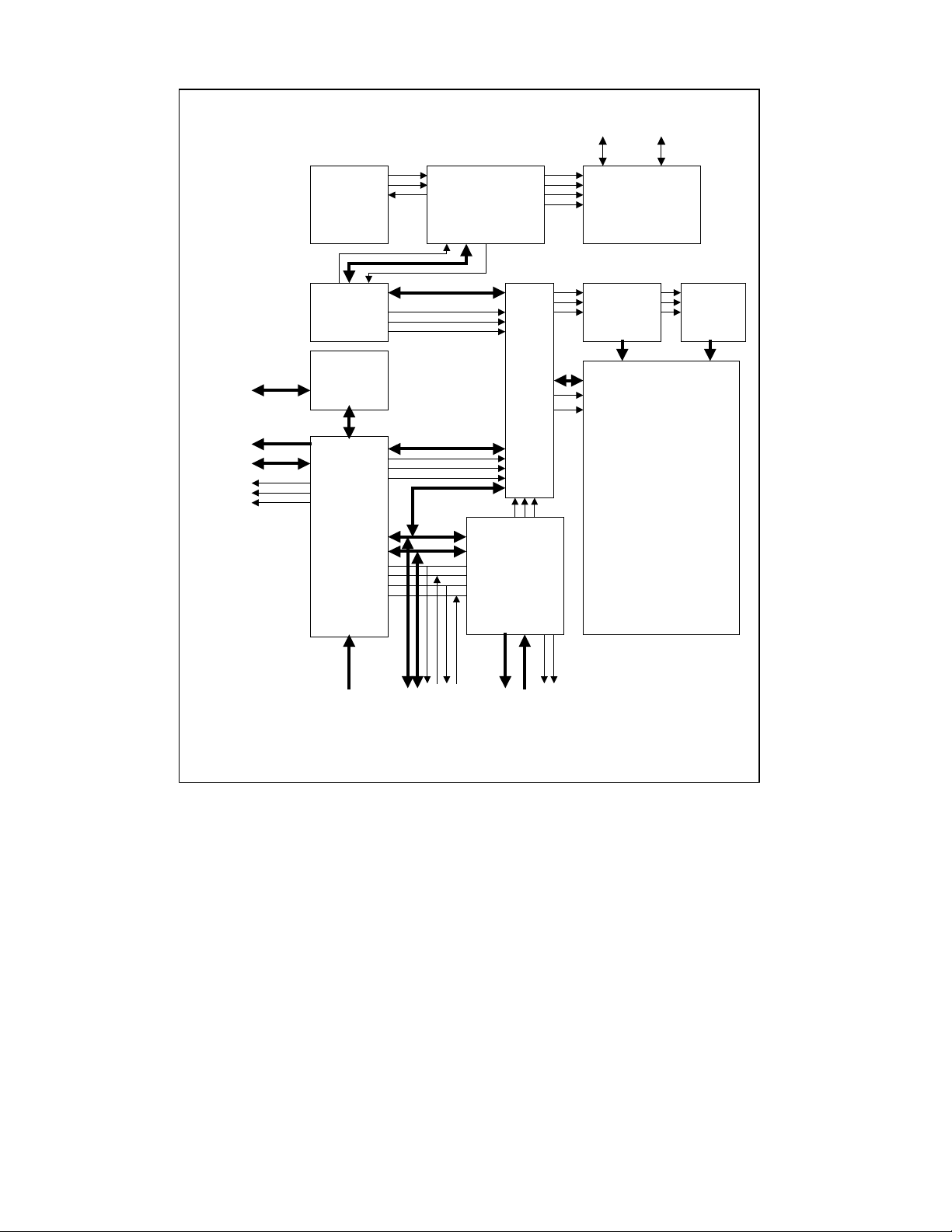
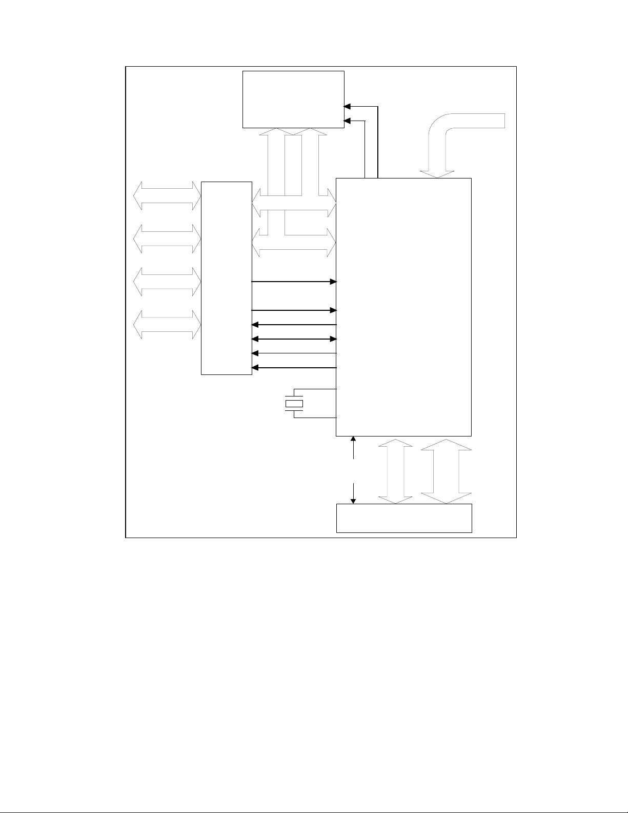
USB97C100 BLOCK DIAGRAM
USB Interface
USBD- USBD+
General
Purpose
IO
GPIO[0:7]
FD[7:0]
FA[19:0]
nFRD
nFWR
nFCE
Flash
Interface
End Point
Control
SIE DMA
Rx/TX
Queue
GPIO
8051
Serial Interfa c e
Engine
Arbiter
8237
Tranceiver
Memory
Management
Unit
4k Data Buffer RAM
Map RAM
IRQ[3:0]
SD[7:0],
SA[19:0]
nIOW,
nIOR,
nMEMW,
nMEMR
DRQ[3:0],
nDACK[3:0],
TC, AEN
Quasi ISA Bus
FIGURE 2 - BLOCK DIAGRAM
SMSC DS – USB97C100 Page 8 Rev. 01/03/2001

FUNCTIONAL DESCRIPTION
The USB97C100 incorporates a USB Serial Interface Engine (SIE), 8051 Microcontroller Unit (MCU), Serial Interface
Engine DMA (SIEDMA), a programmable 8237 ISA bus DMA controller (ISADMA), 4K bytes of SRAM for data
stream buffering, and a patented MMU (Memory Management Unit) to dynamically manage buffer allocation. The
semi-automatic nature of the SIEDMA, ISADMA, and MMU blocks frees the MCU to provide enumeration, protocol
and power management. A bus arbiter integrated into the MMU assures that transparent access between the
SIEDMA, ISADMA, and MCU to the SRAM occurs.
Serial Interface Engine (SIE)
The SIE is a USB low-level protocol interpreter. The SIE controls the USB bus protocol, packet
generation/extraction, parallel-to-serial/serial-to-parallel conversion, CRC coding/decoding, bit stuffing, and NRZI
coding/decoding.
The SIE can be dynamically configured as having any combination of 0-16 transmit, and 0-16 receive endpoints, for
up to 4 independent addresses. There are 3 alternate and one local address. The alternate addresses, for example,
can be used for Hub addresses. The SIE can also "Receive All Addresses" for bus snooping.
Micro Controller Unit (MCU)
The 8051 embedded controller is a static CMOS MCU which is fully software compatible with the industry standard
Intel 80C51 micro-controller. All internal registers of the USB97C100 blocks are mapped into the external memory
space of the MCU.
A detailed description of the microcontroller’s internal registers and instruction set can be found in the “USB97C100
Programmer’s Reference Guide”.
SIEDMA
This is a simplified DMA controller, which automatically transfers data between SIE and SRAM via MMU control. The
SIEDMA appends a status header containing frame number, endpoint, and byte count to each incoming packet
before notifying the MCU of its arrival. This block’s operation is transparent to the firmware.
Memory Management Unit (MMU) Register Description
This patented MMU consists of a 4k buffer RAM which is allocated in 32 pages of 128 bytes. Packets can be
allocated with up to 10 pages each (1280 bytes). The buffer can therefore concurrently hold up to 32 packets with a
64 byte payload. For isochronous pipes, it can hold 3 packets with a 1023 byte payload each, and still have room for
two more 64 byte packets.
This block supports 16 independent transmit FIFO queues (one for each endpoint), and a single receive queue.
Each endpoint can have up to five transmit packets queued. The receive queue can accept 16 packets of any size
combination before forcing the host to back off.
The arbiter makes the single-ported buffer RAM appear to be simultaneously available to the MCU, the four channels
of the ISADMA, and the SIEDMA for receiving and transmitting packets.
ISADMA
This is an industry standard 8237 DMA controller to transfer data between the ISA bus and the SRAM under MMU
control. This DMA contains status and control registers which can be accessed and programmed by the 8051
controller. The 8237 can run at 2, 4, or 8 MHz internally, or via an external clock to synchronize it with another
source.
SMSC DS – USB97C100 Page 9 Rev. 01/03/2001
Applications
The USB97C100 enables entirely new I/O applications, as well as new form factors for existing Legacy I/O
applications. PC98 compliance encourages the elimination ofDMA, IRQ and addressing conflicts via total on-board
ISA elimination. With the USB97C100, the ISA bus can be eliminated from motherboards without sacrificing the
huge infrastructure of Legacy I/O ports. By moving these devices to the flexible USB bus, new form factors such as
monitor peripheral clusters are also possible (mouse, keyboard, serial, parallel ports in a USB connected monitor).
PC system designers are no longer constrained by the physical borders of the motherboard. The USB97C100 is
ideal for USB peripherals which require considerable bandwidth, such as floppy drives, audio, IR, etc. The following
block diagrams illustrate these applications.
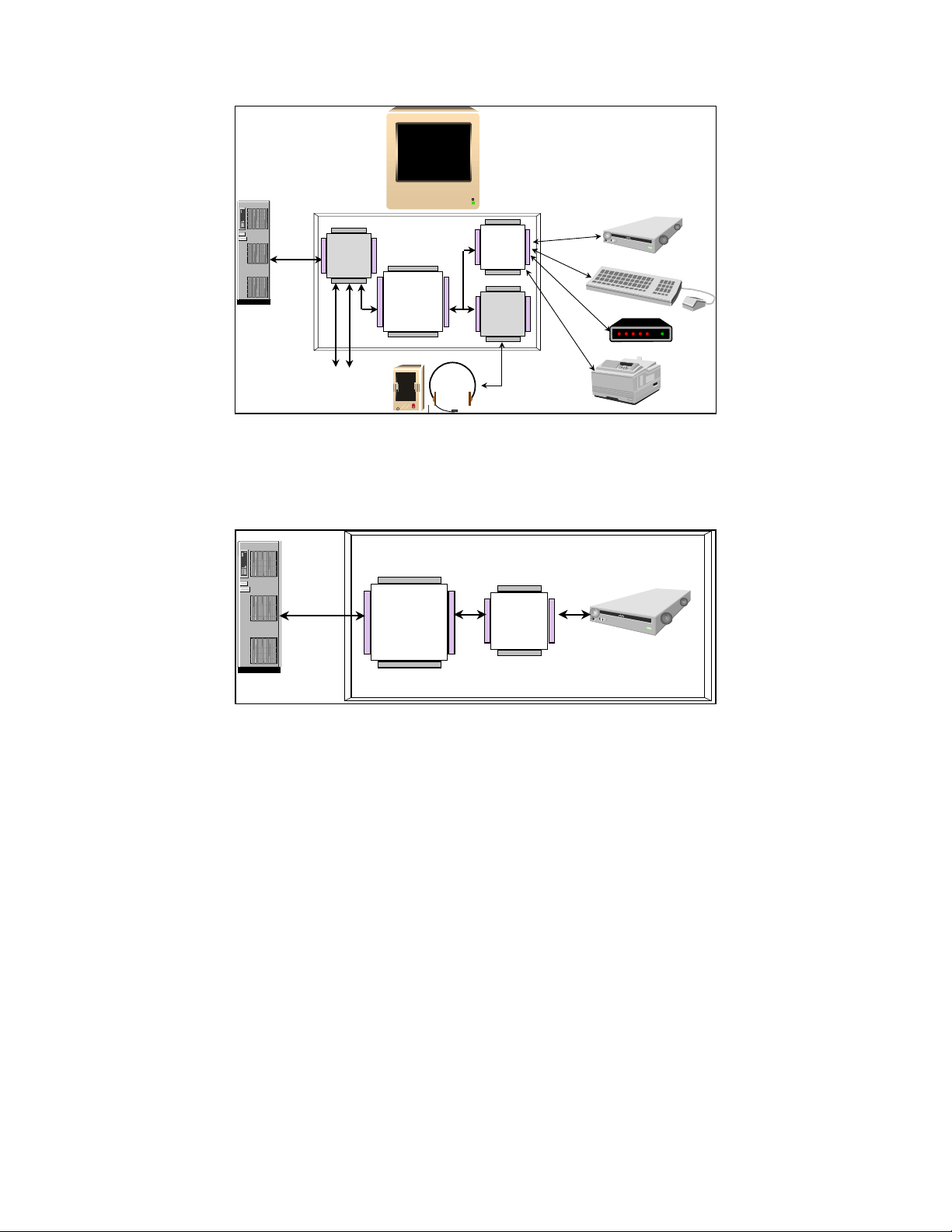
TYPICAL PC MOTHERBOARD APPLICATION
USB
South
USB
Bridge
97C100
Commanche
37C67X
SIO
Floppy
PS/2
Serial
Para llel
FIR
ISA AUDIO
SPKR
MIC
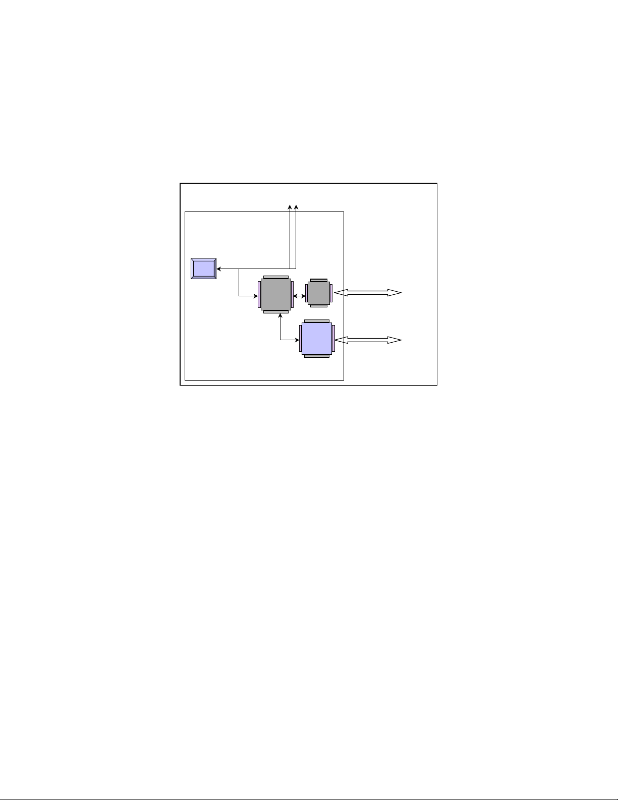
SMSC DS – USB97C100 Page 10 Rev. 01/03/2001
USB
TYPICAL MONITOR APPLICATION
USB HUB
(opt.)
USB
EXPANSION
97C100
Commanche
37C67X
SIO
ISA
CODEC
PARALLEL
TYPICAL FLOPPY DRIVE APPLICATION
FLOPPY
PS/2
SERIAL/FIR
USB
97C100
Commanche
37C78
FDC
SMSC DS – USB97C100 Page 11 Rev. 01/03/2001
TYPICAL SIGNAL CONNECTIONS
SRAM
nMEMW
USB UPSTREAM
nMEMR
FDC
LPT
UART
IR
FDC
37C669FR
SD[7..0]
SA[10..0]
IRQ[3..0]
nDACK[3..0]
DRQ[3..0]
TC
nIOR
nIOW
24MHz
nFRD
nFWR
nFCE
USB97C100
FD[7..0]
FA[19..0]
FLASH
SMSC DS – USB97C100 Page 12 Rev. 01/03/2001
MCU Memory Map
The 64K memory map is as follows from the 8051's viewpoint:
Code Space
Table 3 - MCU Code Memory Map
8051 ADDRESS CODE SPACE ACCESS
0xC000-0xFFFF Movable 16k page External FLASH
0x8000-0xBFFF Fixed 16k page External FLASH
0x7000-0x7FFF Movable 16k FLASH page 1 of 64 16k pages in External FLASH
0x6000-0x6FFF External FLASH (0x00000-0xFFFFF) selected by External FLASH
0x5000-0x5FFF MEM_BANK Register Default: 0x04000- External FLASH
0x4000-0x4FFF 0x07FFFFLASH External FLASH
0x3000-0x3FFF Fixed 16k FLASH Page External FLASH
0x2000-0x2FFF 0x00000-0x03FFF FLASH External FLASH
0x1000-0x1FFF External FLASH
0x0000-0x0FFF External FLASH
Data Space
Table 4 - MCU Data Memory Map
8051 ADDRESS DATA SPACE ACCESS
0xC000-0xFFFF Movable 16k page
Default : 0x04000-0x07FFF FLASH
0x8000-0xBFFF Fixed 16k page
0x00000-0x03FFF FLASH
0x7000-0x7FFF 0x7F80-0x7F9F SIE Reg
0x7F70-0x7F7F ISA Reg
0x7F50-0x7F6F MMU Reg
0x7F20-0x7F2F Power Reg
0x7F10-0x7F1F Configuration Reg
0x7F00-0x7F0F Runtime Reg
Note 1.
0x6000-0x6FFF 0x6000
MMU Data Register
0x5000-0x5FFF 0x5000-0x5FFF
ISA MEMORY Window
0x4000-0x4FFF 0x4000-0x40FF
ISA I/O Window
0x3000-0x3FFF Not used
0x2000-0x2FFF Not used
0x1000-0x1FFF Not used
0x0000-0x00FF Registers and SFR’s Internal
External FLASH
External FLASH
Internal
Internal
ISA
ISA
Note 1: The MCU, MMU, and SIE block registers are external to the 8051, but internal to the USB97C100. These
addresses will appear on the FLASH bus, but the read and write strobes will be inhibited.
ISADMA Memory Map
The Internal Memory buffer is virtualized into the 8237's 64K address map as 32 independent 1k blocks. After the
MMU has allocated a given packet size for a specific PNR, the MMU will make that packet appear to the 8237 as a
contiguous block of data in the address ranges depicted in table 5.
Table 5 - ISADMA Memory Map
8237 MEMORY ADDRESS DESCRIPTION
0x8000-0xFFFF 32 blocks of 1k Window to Packet
0x0000-0x7FFF 32K Window to External ISA RAM
SMSC DS – USB97C100 Page 13 Rev. 01/03/2001

MCU Block Register Summary
ADDRESS NAME R/W DESCRIPTION
7F00 ISR_0 R INT0 Source Register
7F01 IMR_0 R/W INT0 Mask Register
7F02 ISR_1 R INT1 Source Register
7F03 IMR_1 R/W INT1 Mask Register
7F06 DEV_REV R Device Revision Register
7F07 DEV_ID R Device ID Register
7F18 GPIOA_DIR R/W GPIO Configuration Register
7F19 GPIOA_OUT R/W GPIO Data Output Register
7F1A GPIOA_IN R GPIO Data Input Register
7F1B UTIL_CONFIG R/W Miscellaneous Configuration Register
7F27 CLOCK_SEL R/W 8051 and 8237 Clock Select Register
7F29 MEM_BANK R/W Flash Bank Select
7F2A WU_SRC_1 R Wakeup Source
7F2B WU_MSK_1 R/W Wakeup Mask
7F2C WU_SRC_2 R Wakeup Source
7F2D WU_MSK_2 R/W Wakeup Mask
7F10 GP1Data R/W GP FIFO Data Port #1
7F11 GP1Status R GP FIFO status Port #1
7F12 GP2Data R/W GP FIFO Data Port #2
7F13 GP2Status R GP FIFO status Port #2
7F14 GP3Data R/W GP FIFO Data Port #3
7F15 GP3Status R GP FIFO status Port #3
7F16 GP4Data R/W GP FIFO Data Port #4
7F17 GP4Status R GP FIFO status Port #4
7F70 BUS_REQ R/W ISA Bus Request Register
7F71 IOBASE R/W 8051 ISA I/O Window Base Register
7F72 MEMBASE R/W 8051 ISA Memory Window Base Register
7F73 BUS_STAT R ISADMA Request Status
7F74 BUS_MASK R/W ISADMA Request Interrupt Mask
7F7E MCU_TEST2 N/A Reserved for Test
7F7F MCU_TEST1 N/A Reserved for Test
Table 6 - MCU Block Register Summary
RUNTIME REGISTERS
UTILITY REGISTERS
POWER MANAGEMENT REGISTERS
ISA BUS CONTROL REGISTERS
SMSC DS – USB97C100 Page 14 Rev. 01/03/2001

MMU Block Register Summary
ADDRESS NAME R/W DESCRIPTION
0x6000 MMU_DATA R/W 8051-MMU Data Window Register FIFO
7F50 PRL R/W 8051-MMU Pointer Register (Low)
7F51 PRH R/W 8051-MMU Pointer Register (High) & R/W
7F52 MMUTX_SEL R/W 8051-MMU TX FIFO Select for Commands
7F53 MMUCR W 8051-MMU Command Register
7F54 ARR R 8051-MMU Allocation Result Register
7F55 PNR R/W 8051-MMU Packet Number Register
7F56 PAGS_FREE R/W Pages Free In the MMU
7F57 TX_MGMT R TX Management Register 2
7F58 RXFIFO R RX Packet FIFO Register (All EPs)
7F59 POP_TX R POP TX FIFO
7F60 TXSTAT_A R TX Packet FIFO Status Register (EP0-3)
7F61 TXSTAT_B R TX Packet FIFO Status Register (EP4-7)
7F62 TXSTAT_C R TX Packet FIFO Status Register (EP8-11)
7F63 TXSTAT_D R TX Packet FIFO Status Register (EP12-15)
7F64 MMU_TESTx N/A Reserved for Test
7F65 MMU_TESTx N/A Reserved for Test
7F66 MMU_TESTx N/A Reserved for Test
7F67 TX_MGMT R/W TX Management Register 1
7F6E MMU_TESTx N/A Reserved for Test
7F6F MMU_TESTx N/A Reserved for Test
Table 7 - MMU Block Register Summary
MMU REGISTERS
SMSC DS – USB97C100 Page 15 Rev. 01/03/2001

SIE Block Register Summary
ADDRESS NAME R/W DESCRIPTION
7F80 EP_CTRL0 R/W Endpoint 0 Control Register
7F81 EP_CTRL1 R/W Endpoint 1 Control Register
7F82 EP_CTRL2 R/W Endpoint 2 Control Register
7F83 EP_CTRL3 R/W Endpoint 3 Control Register
7F84 EP_CTRL4 R/W Endpoint 4 Control Register
7F85 EP_CTRL5 R/W Endpoint 5 Control Register
7F86 EP_CTRL6 R/W Endpoint 6 Control Register
7F87 EP_CTRL7 R/W Endpoint 7 Control Register
7F88 EP_CTRL8 R/W Endpoint 8 Control Register
7F89 EP_CTRL9 R/W Endpoint 9 Control Register
7F8A EP_CTRL10 R/W Endpoint 10 Control Register
7F8B EP_CTRL11 R/W Endpoint 11 Control Register
7F8C EP_CTRL12 R/W Endpoint 12 Control Register
7F8D EP_CTRL13 R/W Endpoint 13 Control Register
7F8E EP_CTRL14 R/W Endpoint 14 Control Register
7F8F EP_CTRL15 R/W Endpoint 15 Control Register
7F90 FRAMEL R USB Frame Count Low
7F91 FRAMEH R USB Frame Count High
7F92 SIE_ADDR R/W USB Local Address Register
7F93 SIE_STAT R SIE Status Register
7F94 SIE_CTRL R/W SIE Control Register
7F95 SIE_TST1 R/W Reserved Test Register
7F96 SIE_TST2 R/W Reserved Test Register
7F97 SIE_EP_TEST R/W Reserved Test Register
7F98 SIE_CONFIG R/W SIE Configuration Register
7F99 ALT_ADDR1 R/W Secondary Local Address Register #1
7F9A SIE_TST3 R/W Reserved Test Register
7F9B SIE_TST4 R/W Reserved Test Register
7F9C SIE_TST5 R/W Reserved Test Register
7F9D SIE_TST6 R/W Reserved Test Register
7F9E ALT_ADDR2 R/W Secondary Local Address Register #2
7F9F ALT_ADDR3 R/W Secondary Local Address Register #3
Table 8 - SIE Block Register Summary
SIE Control Registers
SMSC DS – USB97C100 Page 16 Rev. 01/03/2001

MCU REGISTER DESCRIPTION
MCU Runtime Registers
ISR_0
(0x7F00 - RESET=0x00) INTERRUPT 0 SOURCE REGISTER
BIT NAME R/W DESCRIPTION
7 IRQ3 R External interrupt input.
6 IRQ2 R External interrupt input.
5 IRQ1 R External interrupt input.
4 IRQ0 R External interrupt input.
3 RX_PKT R 1 = A Packet Number (PNR) has been successfully queued
2 TX_EMPTY R 1 = Whenever an enabled TX Endpoint's FIFO becomes
1 TX_PKT R 1 = A Packet was successfully transmitted.
0 ISADMA R 1 = When a selected 8237 channels in
Table 9 - Interrupt 0 Source Register
0 = Inactive
1 = Active
0 = Inactive
1 = Active
0 = Inactive
1 = Active
0 = Inactive
1 = Active
on the RXFIFO.
empty. This will occur when the last queued packet in one of
the 16 TX queues is successfully transferred to the Host.
BUS_STAT/BUS_MASK register pair either reached Terminal
Count or have a new DMA Request Pending.
These bits are automatically cleared each time this register is read. Therefore, each time this register is read all
pending interrupts must be serviced before continuing normal operation.
Notes:
TX_EMPTY is useful for warning of USB performance degradation. This interrupt indicates that the next time the
Host polls the affected endpoint, it will receive a NAK for that endpoint, thus reducing effective overall bandwidth
due to retries. Firmware must use TX_STAT A, B, and C to determine which endpoint queue is empty.
When ISADMA causes an interrupt, the 8237 CH_STAT register should also be read and serviced when the bit
causing the interrupt is to be rearmed. When ISR_0 is read and the ISADMA bit is cleared, any other low-to-high
transitions in the BUS_STAT register bits that are not masked will still cause an interrupt.
SMSC DS – USB97C100 Page 17 Rev. 01/03/2001

Table 10 - Interrupt 0 Mask
IMR_0
(0x7F01- RESET=0xFF) INTERRUPT 0 MASK REGISTER
BIT NAME R/W DESCRIPTION
7 IRQ3 R/W External interrupt input mask
0 = Enable Interrupt
1 = Mask Interrupt
6 IRQ2 R/W External interrupt input mask
0 = Enable Interrupt
1 = Mask Interrupt
5 IRQ1 R/W External interrupt input mask
0 = Enable Interrupt
1 = Mask Interrupt
4 IRQ0 R/W External interrupt input mask
0 = Enable Interrupt
1 = Mask Interrupt
3 RX_PKT R/W Received Packet MMU Interrupt Mask
0 = Enable Interrupt
1 = Mask Interrupt
2 TX_EMPTY R/W Transmit Queue Empty MMU Interrupt
0 = Enable Interrupt
1 = Mask Interrupt
1 TX_PKT R/W Transmit Packet MMU Interrupt Mask
0 = Enable Interrupt
1 = Mask Interrupt
0 ISADMA R/W ISADMA Status Change Interrupt Mask
0 = Enable Interrupt
1 = Mask Interrupt
Table 11 - Interrupt 1 Source Register
ISR_1
(0x7F02- RESET=0x00) INTERRUPT 1 SOURCE REGISTER
BIT NAME R/W DESCRIPTION
[7:5] Reserved Reserved
4 EOT R 1 = The SIE returned to Idle State. Marks the end of each
transaction.
3 SOF R 1 = When a Start of Frame token is correctly decoded.
Generated by the write strobe to the Frame Count register.
2 ALLOC R 1 = MCU Software Allocation Request complete interrupt. This
interrupt is not generated for hardware (SIEDMA) allocation
requests.
1 RX_OVRN R 1 = A receive condition has occurred that will stop the current
receive buffer to not be processed The SIE automatically
recovers from this condition after its cause has been
alleviated (e.g. any partially allocated packets will be released.
See Note 2).
0 PWR_MNG R 1 = A wakeup or power management event in the WU_SRC_1
or WU_SRC_2 registers has gone active.
Notes:
These bits are cleared each time this register is read.
The RX_OVRN interrupt should be considered by firmware as a general Receive Overrun of the SIE, meaning
that a packet destined for the RAM buffer could not be received and was not acknowledged back to the Host.
The firmware should check to see if the RX Packet Number FIFO Register (RXFIFO) is full. If it is empty, then
there may be too many transmit packets queued for the device to receive anything, or the last packet may have
been corrupted on the wire. If it is not empty, then one or more receive packets must be dequeued before the
device can continue to receive packets. In the normal course of operation, the MCU should respond to a
RX_PKT interrupt as often as possible and let the buffering logic do its job.
SMSC DS – USB97C100 Page 18 Rev. 01/03/2001

Table 12 - Interrupt 1 Mask
IMR_1
(0x7F03- RESET=0xFF) INTERRUPT 1 MASK REGISTER
BIT NAME R/W DESCRIPTION
[7:5] Reserved Reserved
4 EOT R/W EOT interrupt mask
0 = Enable Interrupt
1 = Mask Interrupt
3 SOF R/W Start of Frame Interrupt Mask
0 = Enable Interrupt
1 = Mask Interrupt
2 ALLOC R/W MCU Software Allocation Complete Interrupt Mask
0 = Enable Interrupt
1 = Mask Interrupt
1 RX_OVRN R/W Receive Overrun Interrupt Mask
0 = Enable Interrupt
1 = Mask Interrupt
0 PWR_MNG R/W Power Management Wakeup Interrupt Mask
0 = Enable Interrupt
1 = Mask Interrupt
Table 13 - Device Revision Register
DEV_REV
(0x7F06- RESET=0xXX) DEVICE REVISION REGISTER
BIT R/W DESCRIPTION
[7:0] Rev. R This register defines additional revision information
used internally by SMSC. The value is silicon revision
dependent.
Table 14 - Device Identification Register
DEV_ID
(0x7F07- RESET=0x25) DEVICE IDENTIFICATION REGISTER
BIT R/W DESCRIPTION
[7:0] BCD '25'
HEX 0x25
R This register defines additional revision information
used internally by SMSC
Table 15– 8051 GP FIFO1
GP_FIFO1
(0x7F10- RESET=0xXX) 8051 GP FIFO1
BIT NAME R/W DESCRIPTION
[7:0] GP_FIFO1 R/W 8 byte deep GP FIFO. This data FIFOs must not be read
unless the associated status bit indicates that FIFO is not
empty.
Table 16– 8051 GP FIFO2
GP_FIFO2
(0x7F12 - RESET=0xXX) 8051 GP FIFO2
BIT NAME R/W DESCRIPTION
[7:0] GP_FIFO2 R/W 8 byte deep GP FIFO. This data FIFOs must not be read
unless the associated status bit indicates that FIFO is not
empty.
Table 17– 8051 GP FIFO3
GP_FIFO3
(0x7F14 - RESET=0xXX) 8051 GP FIFO3
BIT NAME R/W DESCRIPTION
[7:0] GP_FIFO3 R/W 8 byte deep GP FIFO. This data FIFOs must not be read
unless the associated status bit indicates that FIFO is not
empty.
SMSC DS – USB97C100 Page 19 Rev. 01/03/2001

GP_FIFO4
(0x7F16 - RESET=0xXX) 8051 GP FIFO4
BIT NAME R/W DESCRIPTION
[7:0] GP_FIFO4 R/W 8 byte deep GP FIFO. This data FIFOs must not be read
FIFO Status Registers
(0x7F11 – RESET=0x01) 8051 GP FIFO status
BIT NAME R/W DESCRIPTION
[7:2] Reserved R Reserved
1 GPFIFO1_FULL R GP FIFO 1 full status
0 GPFIFO1_EMPTY R GP FIFO 1 empty status
(0x7F13 – RESET=0x01) 8051 GP FIFO 2 status
BIT NAME R/W DESCRIPTION
[7:2] Reserved R Reserved
1 GPFIFO2_FULL R GP FIFO 2 full status
0 GPFIFO2_EMPTY R GP FIFO 2 empty status
Table 18 – 8051 GP FIFO4
unless the associated status bit indicates that FIFO is not
empty.
Table 19 – 8051 GP FIFO 1 STATUS
GPFIFO1_STS
0 = Not FULL
1 = FULL
0 = Has one or more TX packet
1 = Empty
Table 20– 8051 GP FIFO 2 STATUS
GPFIFO2_STS
0 = Not FULL
1 = FULL
0 = Has one or more TX packet
1 = Empty
Table 21 – 8051 GP FIFO 3 STATUS
GPFIFO3_STS
(0x7F15 – RESET=0x01) 8051 GP FIFO 3 status
BIT NAME R/W DESCRIPTION
[7:2] Reserved R Reserved
1 GPFIFO3_FULL R GP FIFO 3 full status
0 = Not FULL
1 = FULL
0 GPFIFO3_EMPTY R GP FIFO 3 empty status
0 = Has one or more TX packet
1 = Empty
Table 22 – 8051 GP FIFO 4 STATUS
GPFIFO4_STS
(0x7F17 – RESET=0x01) 8051 GP FIFO status
BIT NAME R/W DESCRIPTION
[7:2] Reserved R Reserved
1 GPFIFO4_FULL R GP FIFO 4 full status
0 = Not FULL
1 = FULL
0 GPFIFO4_EMPTY R GP FIFO 4 empty status
0 = Has one or more TX packet
1 = Empty
SMSC DS – USB97C100 Page 20 Rev. 01/03/2001

Table 23 - GPIO Direction Register
GPIOA_DIR
(0x7F18- RESET=0x00) MCU UTILITY REGISTERS
BIT NAME R/W DESCRIPTION
7 GPIO7 R/W GPIO7 Direction
0 = In
1 = Out
6 GPIO6 R/W GPIO6 Direction
0 = In
1 = Out
5 GPIO5 R/W GPIO5 Direction
0 = In
1 = Out
4 GPIO4 R/W GPIO4 Direction
0 = In
1 = Out
3 GPIO3/T1 R/W GPIO3 Direction
0 = In
1 = Out
2 GPIO2/T0 R/W GPIO2 Direction
0 = In
1 = Out
1 GPIO1/TXD R/W GPIO1 Direction
0 = In
1 = Out
0 GPIO0/RXD R/W GPIO0 Direction
0 = In
1 = Out
Note: The Timer inputs T[1:0] can be configured as outputs and left unconnected so that software can write to the
bits to trigger the timer. Otherwise, the Timer inputs can be used to count external events or internal SOF
receptions.
Table 24 - GPIO Output Register
GPIOA_OUT
(0x7F19- RESET=0x00)
GPIO DATA OUTPUT
REGISTER A
BIT NAME R/W DESCRIPTION
7 GPIO7 R/W GPIO7 Output Buffer Data
6 GPIO6 R/W GPIO6 Output Buffer Data
5 GPIO5 R/W GPIO5 Output Buffer Data
4 GPIO4 R/W GPIO4 Output Buffer Data
3 GPIO3/T1 R/W GPIO3 Output Buffer Data
2 GPIO2/T0 R/W GPIO2 Output Buffer Data
1 GPIO1/TXD R/W GPIO1 Output Buffer Data
0 GPIO0/RXD R/W GPIO0 Output Buffer Data
Table 25 - GPIO Input Register
GPIOA_IN
(0x7F1A- RESET=0xXX) GPIO INPUT REGISTER A
BIT NAME R/W DESCRIPTION
7 GPIO7 R GPIO7 Input Buffer Data
6 GPIO6 R GPIO6 Input Buffer Data
5 GPIO5 R GPIO5 Input Buffer Data
4 GPIO4 R GPIO4 Input Buffer Data
3 GPIO3/T1 R GPIO3 Input Buffer Data
2 GPIO2/T0 R GPIO2 Input Buffer Data
1 GPIO1/TXD R GPIO1 Input Buffer Data
0 GPIO0/RXD R GPIO0 Input Buffer Data
SMSC DS – USB97C100 Page 21 Rev. 01/03/2001

Table 26 - Utility Configuration Register
UTIL_CONFIG
(0x7F1B- RESET=0x00) UTILITY CONFIGURATION REGISTER
BIT NAME R/W DESCRIPTION
[7:4] Reserved R Reserved
3 GPIO3/T1 R/W P3.5 Timer 1 input trigger source
0 = GPIO3
1 = SOF FRAME write strobe
2 GPIO2/T0 R/W P3.4 Timer 0 input trigger source
0 = GPIO2
1 = SOF FRAME write strobe
1 GPIO1/TXD R/W GPIO1/TXD Output Select Mux
0 = GPIO1
1 = P3.1
0 GPIO0/RXD R/W P3.0 RXD/GPIO0 Input Select Mux
0 = RXD<=GPIO0
1 = RXD<='0'
Notes:
In Counter mode, the 8051 must sample T[1:0] as a '1' in one instruction cycle, and then '0' in the next. So for
12MHz, the SOF Pulse must be active for at least 1us.
Missing SOF packets can be reconstructed by using the Timer mode to count the number of 8051 instruction
cycles since the last valid Frame was received.
A GPIO can be used to output nSOF pulses. This can be done by configuring a GPIO as an output and writing
to the GPIO out register to generate low pulses each time a SOF packet is received.
SMSC DS – USB97C100 Page 22 Rev. 01/03/2001
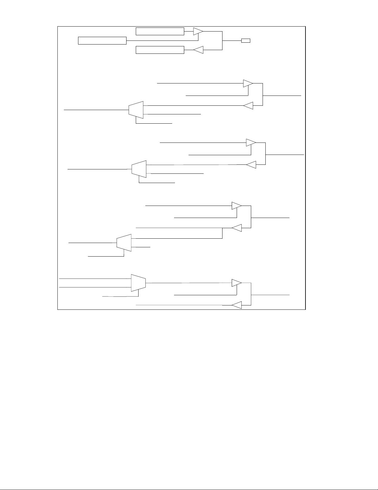
])
[0]
])
])
])
[1]
])
])
]
])
])
])
]
])
])
])
]
GPIO Direction Bit
(
])
(
])
(
])
0x7F18[7:4
GPIO out data
0x7F19[7:4
GPIO in data
0x7F1A[7:4
GPIO2 data out (0x7F19[2
GPIO[7:4
8051 "T0 timer P3.4"
8051 "T1 timer P3.5"
RXD "Uart P3.0"
0X7F1B
GPIO2 data in (0x7F1A[2
0
Internal SOF
1
S
0X7F1B[2
GPIO3 data out (0x7F19[3
GPIO3 data in (0x7F1A[3
0
Internal SOF
1
S
0X7F1B[3
GPIO0 data out (0x7F19[0
GPIO0 data in (0x7F1A[0
0
"0"
1
S
GPIO2 Dir (0x7F18[2
GPIO3 Dir (0x7F18[3
GPIO0 Dir (0x7F18[0
Pin # 36
Pin # 37
Pin # 34
GPIO1 data out (0x7F19[1
TXD "Uart P3.1"
0X7F1B
0
1
S
GPIO1 Dir (0x7F18[1
Pin # 35
GPIO1 data in (0x7F1A[1
FIGURE 3 - GPIO MUXING BLOCK DIAGRAM
SMSC DS – USB97C100 Page 23 Rev. 01/03/2001

MCU Power Management Registers
Table 27 - MCU/ISADMA Clock Source Select
CLOCK_SEL
(0x7F27 - RESET=0x40) MCU/ISADMA CLOCK SOURCE SELECT
BIT NAME R/W DESCRIPTION
7 SLEEP R/W When PCON. 0 = 1 and SLEEP has been set to 1, the
ring oscillator will be gated off, then all oscillators will be
turned off for maximum power savings. (These two signals
can be used to generate nFCE)
6 ROSC_EN R/W 0 = Ring Oscillator Disable.
1 = Ring Oscillator Enable. ROSC_EN must be set to 1
before the MCU can be switched to the internal Ring
Oscillator Clock source.
5 MCUCLK_SRC R/W MCUCLK_SRC overrides MCUCLK_x clock s elect and
switches the MCU to the Ring Oscillator.
0 = Use Ring Oscillator. ROSC_EN must be enabled by
the MCU first.
1 = Use clock specified in MCU_CLK_[1:0]
[4:3] MCU_CLK[1:0] R/W [4:3] = 00: 8MHz
[4:3] = 01: 12MHz
[4:3] = 10: 16MHz
[4:3] = 11: 24MHz
2 ISADMACLK_EXT R/W Selects an external clock source for the 8237 ISADMA
controller for synchronizing the DMA with another block.
NOTE: This will initially be an external input, but may
eventually be used within the block to optimize
performance, or as some other internal clock source.
0 = Use ISADMACLK[1..0] select
1 = Use EXT_IN clock source for 8237
[1:0] ISADMACLK[1:0] R/W [1:0] = 00: Stopped
[1:0] = 01: 2MHz
[1:0] = 10: 4MHz
[1:0] = 11: 8MHz
Notes:
The 8051 may program itself to run off of an internal Ring Oscillator having a frequency range between 4 and
12MHz. This is not a precise clock, but is meant to provide the 8051 with a clock source, without running the
24MHz crystal oscillator or the PLL
Switching between fast and slow clocks is recommended to save pow er.
Clock switching can be done on the fly as long as both clocks are running. When switching, it takes a total of six
clocks (3 clocks of the original clock plus 3 clocks of the switching clock) to guarantee the switching.
Time TBD is required from ROSC_EN=1 to MCUCLK_SRC=0.
SMSC DS – USB97C100 Page 24 Rev. 01/03/2001

Table 28 - FLASH Bank Select Register
MEM_BANK
(0x7F29 - RESET=0x01) FLASH BANK SELECT REGISTER
BIT NAME R/W DESCRIPTION
[7:6] Reserved R Reserved
[5:0] A[19:14] R/W This register selects which 16k page resides at 0x4000-0x7FFF in Code
Space and 0xC000-0xFFFF in Data Space. The 0x0000-0x3FFF page
will always reflect the 16K FLASH page 0 (0x00000-0x03FFF).
Table 29 - Wakeup Source 1 Register
WU_SRC_1
(0x7F2A - RESET=0x00) WAKEUP SOURCE 1
BIT NAME R/W DESCRIPTION
[7:3] Reserved R Reserved
2 USB_Reset R This bit is set when the SIE detects simultaneous logic lows on D+
and D- (Single-Ended 0) for 32 to 64 full speed bit times, or 4 to 8 low
speed bit times (or 2.5<t<5.5us). The USB_Reset signal may be as
long as 10ms. SETUP tokens can be NAK'd for up to 10ms after the
Reset signal is released.
1 Resume R This bit is set on detection of Global Resume state (when there is a
transition from the "J" state while in Global Suspend).
0 Reserved '0' R Reserved
Notes:
Only low to high transitions for the associated inputs sets these bits.
These bits are cleared each time this register is read.
Unmasked W akeup Source bits generate an INT1 PWR_MNG interrupt, and restart the 8051 when its clock is
stopped. This restarts the Ring Oscillator and crystal oscillator for the MCU to resume from <500µA operation.
To initiate USB Remote Wakeup, the SIE_Resume bit should be used in the SIE_CONFIG register.
Table 30 - Wakeup Mask 1 Register
WU_MSK_1 (Note 1)
(0x7F2B - RESET=0x07 ) WAKEUP MASK 1
BIT NAME R/W DESCRIPTION
[7:3] Reserved R Reserved
2 USB_Reset R/W External wakeup event.
0 = Enabled
1 = Masked
1 Resume R/W External wakeup event.
0 = Enabled
1 = Masked
0 Reserved R Reserved
Note: Interrupt events enabled by these bits are routed to the PWR_MNG Bit 0 in the ISR_1 register.
SMSC DS – USB97C100 Page 25 Rev. 01/03/2001

Table 31 - Wakeup Source 2 Register
WU_SRC_2
(0x7F2C - RESET=0x00) WAKEUP SOURCE 2
BIT NAME R/W DESCRIPTION
[7:4] '0' R Reserved
3 IRQ3 R External Interrupt state since WU_SRC_2 was last read.
0 = Unchanged
1 = Changed
2 IRQ2 R External Interrupt state since WU_SRC_2 was last read.
0 = Unchanged
1 = Changed
1 IRQ1 R External Interrupt state since WU_SRC_2 was last read.
0 = Unchanged
1 = Changed
0 IRQ0 R External Interrupt state since WU_SRC_2 was last read.
0 = Unchanged
1 = Changed
Notes:
Any transition from high to low, or low to high on the associated input sets these bits. These bits are cleared
each time this register is read.
Since this register will report any status change, when devices are to be powered down while monitored, the
appropriate bits must be masked until the device is armed correctly.
Table 32 - Wakeup Mask 2 Register
WU_MSK_2
(0x7F2D - RESET=0x0F) WAKEUP MASK 2
BIT NAME R/W DESCRIPTION
[7 :4] '0' R Reserved
3 IRQ3 R/W External wakeup event enable.
0 = Enabled
1 = Masked
2 IRQ2 R/W External wakeup event enable.
0 = Enabled
1 = Masked
1 IRQ1 R/W External wakeup event enable.
0 = Enabled
1 = Masked
0 IRQ0 R/W External wakeup event enable.
0 = Enabled
1 = Masked
Note: Interrupt events enabled by these bits are be routed to the PWR_MNG Bit 0 in the ISR_1 register.
SMSC DS – USB97C100 Page 26 Rev. 01/03/2001

MCU ISA Interface Registers
BUS_REQ
(0x7F70 – RESET=0x00) ISA BUS REQUEST REGISTER
BIT NAME R/W DESCRIPTION
7 INH_TC3 R/W This bit inhibits DMA channel 3 TC.**See Note Below
6 INH_TC2 R/W This bit inhibits DMA channel 2 TC.** See Note Below
5 INH_TC1 R/W This bit inhibits DMA channel 1 TC.** See Note Below
4 INH_TC0 R/W This bit inhibits DMA channel 0 TC.** See Note Below
3 RESET_8237 R/W Writing a '1' holds the 8237 hardware reset input active. Writing
2 AEN R This bit reflects the status of the 8237's AEN pin. This bit does
1 HLDA R/W The 8051 can grant the bus when it is ready via HLDA. This
0 HREQ R This bit reflects the status of the 8237's HREQ bus request pin.
Table 33 – ISA Bus Request Register
0 = TC is driven onto the ISA bus via EOP as before.
1 = TC is forced inactive.
0 = TC is driven onto the ISA bus via EOP as before.
1 = TC is forced inactive.
0 = TC is driven onto the ISA bus via EOP as before.
1 = TC is forced inactive.
0 = TC is driven onto the ISA bus via EOP as before.
1 = TC is forced inactive.
'0' releases it for normal operation. May be used for clock
switching or power management functions.
not generate an interrupt
should tri-state any common signals between the 8051 and the
8237 on the ISA bus.
This bit does not generate an interrupt.
Note: HLDA Example: When the 8051 is running at 24MHz, and the 8237 is running at 2MHz, the 8237 may take
up to 1.5us to complete a transfer after deasserting HLDA . When running the 8051 at 24MHz, wait states
must be added when the 8237 is running at 2 or 4 MHz. When running the 8051 at 12MHz, wait states must
be added when the 8237 is running at 2 MHz.
Note**: The “Inhibit” function is not valid for Memory-to-Memory DMA cycles
SMSC DS – USB97C100 Page 27 Rev. 01/03/2001

Table 34 - ISA Bus Status Register
BUS_STAT
(0x7F73 - RESET=0xXX) ISA BUS STATUS REGISTER
BIT NAME R/W DESCRIPTION
7 CH3RQ R Channel 3 DMA Request
0 = No Request Pending
1 = Request Pending
6 CH2RQ R Channel 2 DMA Request
0 = No Request Pending
1 = Request Pending
5 CH1RQ R Channel 1 DMA Request
0 = No Request Pending
1 = Request Pending
4 CH0RQ R Channel 0 DMA Request
0 = No Request Pending
1 = Request Pending
3 CH3TC R Channel 3 Terminal Count Reached
0 = No
1 = Yes
2 CH2TC R Channel 2 Terminal Count Reached
0 = No
1 = Yes
1 CH1TC R Channel 1 Terminal Count Reached
0 = No
1 = Yes
0 CH0TC R Channel 0 Terminal Count Reached
0 = No
1 = Yes
Notes:
Each bit in this register reflects the current value of the corresponding bit in the 8237 CH_STAT status register.
The 8237 clears bits 3..0 in the CH_STAT status register when the 8051 reads it through the ISA Bus I/O
Window.
Reading the BUS_STAT register does not clear or otherwise affect the BUS_STAT register.
The ISADMA bit in ISR_0 is latched high whenever any bit in BUS_STAT that is enabled in BUS_MASK
transitions from low to high.
This register is intended (1) to provide a view into the status of the 8237 without having to assume control of the
ISA bus during DMA transfers, and (2) to provide a means for generating the ISADMA interrupt in ISR_0 which
indicates that a DMA transfer has completed and that the 8051 should take control of the bus and setup the
8237 for its next transfer. Bits 7-4 can be used to generate additional interrupt requests from the DREQ pins, or
simply to monitor channel request status by masking them.
SMSC DS – USB97C100 Page 28 Rev. 01/03/2001

Table 35 - ISA Bus Status Mask Register
BUS_MASK
(0x7F74 - RESET=0xFF) ISA BUS STATUS MASK REGISTER
BIT NAME R/W DESCRIPTION
7 CH3RQ_MASK R/W Channel 3 DMA Request ISADMA Interrupt Mask
0 = Enable Interrupt
1 = Mask Interrupt
6 CH2RQ_MASK R/W Channel 2 DMA Request ISADMA Interrupt Mask
0 = Enable Interrupt
1 = Mask Interrupt
5 CH1RQ_MASK R/W Channel 1 DMA Request ISADMA Interrupt Mask
0 = Enable Interrupt
1 = Mask Interrupt
4 CH0RQ_MASK R/W Channel 0 DMA Request ISADMA Interrupt Mask
0 = Enable Interrupt
1 = Mask Interrupt
3 CH3TC_MASK R/W Channel 3 Terminal Count ISADMA Interrupt Mask
0 = Enable Interrupt
1 = Mask Interrupt
2 CH2TC_MASK R/W Channel 2 Terminal Count ISADMA Interrupt Mask
0 = Enable Interrupt
1 = Mask Interrupt
1 CH1TC_MASK R/W Channel 1 Terminal Count ISADMA Interrupt Mask
0 = Enable Interrupt
1 = Mask Interrupt
0 CH0TC_MASK R/W Channel 0 Terminal Count ISADMA Interrupt Mask
0 = Enable Interrupt
1 = Mask Interrupt
Table 36 - ISA I/O Window Base Register
IOBASE
(0x7F71 - RESET=0x00) ISA I/O WINDOW BASE REGISTER
BIT NAME R/W DESCRIPTION
[7:0] SA[15:8] R/W When the 8051 reads or writes to the ISA I/O Window,
this register is combined with the 8 bit offset in the 256
byte window and presented as the 64k I/O Space address
during an 8051-ISA IOR or IOW cycle
Table 37 - ISA Memory Window Base Register
MEMBASE
(0x7F72 - RESET=0x00) ISA MEMORY WINDOW BASE REGISTER
BIT NAME R/W DESCRIPTION
[7:0] SA[19:12] R/W When the 8051 reads or writes to the ISA Memory
Window, this register is combined with the 12 bit
offset in the 4k byte window and presented as the
1Mbyte Memory address during an 8051-ISA
MEMR or MEMW cycle.
SMSC DS – USB97C100 Page 29 Rev. 01/03/2001

8237 (ISADMA) REGISTER DESCRIPTION
Memory Map
Table 38 - ISADMA Memory Map
8237 MEMORY ADDRESS DESCRIPTION
0xFC00-0xFFFF 1k Window to Packet with PNR=0x1F
0xF800-0xFBFF 1k Window to Packet with PNR=0x1E
0xF400-0xF7FF 1k Window to Packet with PNR=0x1D
0xF000-0xF3FF 1k Window to Packet with PNR=0x1C
0xEC00-0xEFFF 1k Window to Packet with PNR=0x1B
0xE800-0xEBFF 1k Window to Packet with PNR=0x1A
0xE400-0xE7FF 1k Window to Packet with PNR=0x19
0xE000-0xE3FF 1k Window to Packet with PNR=0x18
0xDC00-0xDFFF 1k Window to Packet with PNR=0x17
0xD800-0xDBFF 1k Window to Packet with PNR=0x16
0xD400-0xD7FF 1k Window to Packet with PNR=0x15
0xD000-0xD3FF 1k Window to Packet with PNR=0x14
0xCC00-0xCFFF 1k Window to Packet with PNR=0x13
0xC800-0xCBFF 1k Window to Packet with PNR=0x12
0xC400-0xC7FF 1k Window to Packet with PNR=0x11
0xC000-0xC3FF 1k Window to Packet with PNR=0x10
0xBC00-0xBFFF 1k Window to Packet with PNR=0x0F
0xB800-0xBBFF 1k Window to Packet with PNR=0x0E
0xB400-0xB7FF 1k Window to Packet with PNR=0x0D
0xB000-0xB3FF 1k Window to Packet with PNR=0x0C
0xAC00-0xAFFF 1k Window to Packet with PNR=0x0B
0xA800-0xABFF 1k Window to Packet with PNR=0x0A
0xA400-0xA7FF 1k Window to Packet with PNR=0x09
0xA000-0xA3FF 1k Window to Packet with PNR=0x08
0x9C00-0x9FFF 1k Window to Packet with PNR=0x07
0x9800-0x9BFF 1k Window to Packet with PNR=0x06
0x9400-0x97FF 1k Window to Packet with PNR=0x05
0x9000-0x93FF 1k Window to Packet with PNR=0x04
0x8C00-0x8FFF 1k Window to Packet with PNR=0x03
0x8800-0x8BFF 1k Window to Packet with PNR=0x02
0x8400-0x87FF 1k Window to Packet with PNR=0x01
0x8000-0x83FF 1k Window to Packet with PNR=0x00
0x0000-0x7FFF 32K Window to External ISA RAM
The actual packet may be composed of up to 10 different 128 byte non-contiguous packets, but the MMU re-maps
the internal addresses automatically such that the 8237 and 8051 only need to reference the packet number and
offset within the packet. For example, suppose a 312 (0x138) byte packet is received by the SIEDMA from the host.
The patented MMU allocates 384 bytes for the packet (including an 8 byte status header) and returns a PNR tag of
0x0A. The SIEDMA engine will place 0x0A in the receive packet queue and notify the 8051. The 8051 will take that
PNR, examine the packet through its own PNR/Pointer registers, and determine the offset for the payload data it
wants to transfer from the packet, say 0x027. The address it must calculate for the 8237 base address register would
therefore be 0xA827 (0xA800+0x027). Each channel can be programmed with a different (or same) Packet Number
and offset and the data will appear to it as ordinary contiguous RAM (see table 32 for more information).
Software written to this model will work for virtually any Endpoint number and Buffer size combination.
SMSC DS – USB97C100 Page 30 Rev. 01/03/2001

Runtime Registers
The DMA controller has a block of 16 R/W registers which normally occupy I/O locations 0x00-0x0F on the ISA bus.
When they are located at 0x0000-0x000F on the ISA bus, the 8051 can access them by programming the IOBASE
Register to 0x00, and reading or writing from 0x4000-0x400F.
Table 39 - 8237 Registers in ISA I/O Space
0x0000 Channel 0: Current Address H/L
0x0001 Channel 0: Byte Count H/L
0x0002 Channel 1: Current Address H/L
0x0003 Channel 1: Byte Count H/L
0x0004 Channel 2: Current Address H/L
0x0005 Channel 2: Byte Count H/L
0x0006 Channel 3: Current Address H/L
0x0007 Channel 3: Byte Count H/L
0x0008 Status/Command Register
0x0009 Write Request Register
0x000A Write Single Mask Register
0x000B Write Mode Register
0x000C Clear Byte Ptr F/F - Read Temp
Register
0x000D Master Clear
0x000E Clear Mask
0x000F Write All Mask Bits
Note: To write to these registers, HLDA must be logic low.
SMSC DS – USB97C100 Page 31 Rev. 01/03/2001

Table 40 - 8237 Address Programming Guide
8237 INTERNAL ADDRESS PROGRAMMING GUIDE
BIT NAME DESCRIPTION
15 INT_EXT Indicates whether this address refers to Internal Buffer RAM or
External ISA Memory Space
0 = External
1 = Internal
When this bit is set to zero (0), I/O capability is added to External
Memory DMA. This capability can only be used for DMA channels 2
or 3.
[14:10] PN[4:0]/SA[14:10] External Address -or- Internal Packet Number
SA[14..10] when INT_EXT=0
PN[4..0] when INT_EXT=1
[9:0] PTR[9:0]/SA[9:0] External Address -or- Internal Packet Offset Pointer
SA[9..0] when INT_EXT=0
PTR[9..0] when INT_EXT=1
Note: SA[19..15] are driven low when the 8237 is accessing external ISA memory. PTR10 is driven low when the
8237 is accessing internal buffer RAM. Note that the actual transfer size for the ISADMA is limited to 1024
bytes, which limits the payload data to 1016 bytes per transfer when the 8 byte header is skipped. Also note
that the 8051 still has access to 1Meg of external RAM through the MEMBASE register and it is
independent of the 8237's 32k external limit.
Table 41 - Channel 0 Current Address Register
CH0_ADDR
(ISA 0x0000) CHANNEL 0 CURRENT ADDRESS
BIT NAME R/W DESCRIPTION
[7:0] CH0_ADDRL R/W Lower 8 bits of Base and Current Address when Byte F/F = 0
[7:0] CH0_ADDRH R/W Upper 8 bits of Base and Current Address when Byte F/F = 1
Note: Byte F/F is an internal Flip Flop which reflects which byte (high or low) is being written. The CLEAR_FF
register should be written to before writing this register to guarantee which byte (high or low) is being
written. See the Address Programming Table for 16 bit Address definitions.
Table 42 - Channel 0 Byte Count Register
CH0_CNT
(ISA 0x0001) CHANNEL 0 BYTE COUNT
BIT NAME R/W DESCRIPTION
[7:0] CH0_CNTL R/W Lower 8 bits of Byte Count when Byte F/F = 0
[7:0] CH0_CNTH R/W Upper 8 bits of Byte Count when Byte F/F = 1
Note: The CLEAR_FF register should be written to before writing this register to guarantee which byte (high or
low) is being written. See Address Programming Table for 16 bit Address definitions.
Table 43 - Channel 1 Current Address Register
CH1_ADDR
(ISA 0x0002) CHANNEL 1 CURRENT ADDRESS
BIT NAME R/W DESCRIPTION
[7:0] CH1_ADDRL R/W Lower 8 bits of Base and Current Address when Byte F/F = 0
[7:0] CH1_ADDRH R/W Upper 8 bits of Base and Current Address when Byte F/F = 1
Note: The CLEAR_FF register should be written to before writing this register to guarantee which byte (high or
low) is being written. See the Address Programming Table for 16 bit Address definitions.
SMSC DS – USB97C100 Page 32 Rev. 01/03/2001

Table 44 - Channel 1 Byte Count Register
CH1_CNT
(ISA 0x0003) CHANNEL 1 BYTE COUNT
BIT NAME R/W DESCRIPTION
[7:0] CH1_CNTL R/W Lower 8 bits of Byte Count when Byte F/F = 0
[7:0] CH1_CNTH R/W Upper 8 bits of Byte Count when Byte F/F = 1
Note: The CLEAR_FF register should be written to before writing this register to guarantee which byte (high or
low) is being written. See Address Programming Table for 16 bit Address definitions.
Table 45 - Channel 2 Current Address Register
CH2_ADDR
(ISA 0x0004) CHANNEL 2 CURRENT ADDRESS
BIT NAME R/W DESCRIPTION
[7:0] CH2_ADDRL R/W Lower 8 bits of Base and Current Address when Byte F/F = 0
[7:0] CH2_ADDRH R/W Upper 8 bits of Base and Current Address when Byte F/F = 1
Note: The CLEAR_FF register should be written to before writing this register to guarantee which byte (high or
low) is being written. See the Address Programming Table for 16 bit Address definitions.
Table 46 - Channel 2 Byte Count Register
CH2_CNT
(ISA 0x0005) CHANNEL 2 BYTE COUNT
BIT NAME R/W DESCRIPTION
[7:0] CH2_CNTL R/W Lower 8 bits of Byte Count when Byte F/F = 0
[7:0] CH2_CNTH R/W Upper 8 bits of Byte Count when Byte F/F = 1
Note: The CLEAR_FF register should be written to before writing this register to guarantee which byte (high or
low) is being written. See Address Programming Table for 16 bit Address definitions.
Table 47 - Channel 3 Current Address Register
CH3_ADDR
(ISA 0x0006) CHANNEL 3 CURRENT ADDRESS
BIT NAME R/W DESCRIPTION
[7:0] CH3_ADDRL R/W Lower 8 bits of Base and Current Address when Byte F/F = 0
[7:0] CH3_ADDRH R/W Upper 8 bits of Base and Current Address when Byte F/F = 1
Note: The CLEAR_FF register should be written to before writing this register to guarantee which byte (high or
low) is being written. See the Address Programming Table for 16 bit Address definitions.
Table 48 - Channel 3 Byte Count Register
CH3_CNT
(ISA 0x0007) CHANNEL 3 BYTE COUNT
BIT NAME R/W DESCRIPTION
[7:0] CH3_CNTL R/W Lower 8 bits of Byte Count when Byte F/F = 0
[7:0] CH3_CNTH R/W Upper 8 bits of Byte Count when Byte F/F = 1
Note: The CLEAR_FF register should be written to before writing this register to guarantee which byte (high or
low) is being written. See Address Programming Table for 16 bit Address definitions.
SMSC DS – USB97C100 Page 33 Rev. 01/03/2001

Table 49 - Channel Status Register
CH_STAT
(ISA 0x0008) CHANNEL STATUS REGISTER
BIT NAME R/W DESCRIPTION
7 CH3RQ R Channel 3 DMA Request
0 = No Request Pending
1 = Yes Request Pending
6 CH2RQ R Channel 2 DMA Request
0 = No Request Pending
1 = Yes Request Pending
5 CH1RQ R Channel 1 DMA Request
0 = No Request Pending
1 = Yes Request Pending
4 CH0RQ R Channel 0 DMA Request
0 = No Request Pending
1 = Yes Request Pending
3 CH3TC R Channel 3 Terminal Count Reached
0 = No
1 = Yes
2 CH2TC R Channel 2 Terminal Count Reached
0 = No
1 = Yes
1 CH1TC R Channel 1 Terminal Count Reached
0 = No
1 = Yes
0 CH0TC R Channel 0 Terminal Count Reached
0 = No
1 = Yes
Notes:
These bits are also visible outside of I/O space in the BUS_STAT register.
These bits are cleared when this register is read through the ISA I/O Window.
Table 50 - 8237 Command Register
CH_CMD
(ISA 0x0008) COMMAND REGISTER
BIT NAME R/W DESCRIPTION
7 DACK_SENS W DACK Sense
0 = Active High
1 = Active Low
6 DREQ_SENS W DREQ Sense (1 = Active Low, 0 = Active High)
5 WRITE_TIME W Write Timing Select
0 = Late Timing
1 = Extended
4 PRIORITY W Priority
0 = Fixed
1 = Rotating
3 COMP_TIME W Timing
0 = Normal
1 = Compressed
2 CTRL_EN W Controller Enable
0 = Enable
1 = Disable
1 ADDR_HOLD W Channel 0 Address Hold
0 = Disable
1 = Hold Enable
0 MEM2MEM W Memory-to-Memory
0 = Disable
1 = Enable
SMSC DS – USB97C100 Page 34 Rev. 01/03/2001

Table 51 - 8237 Write Single Request Register
CH_REQ
(ISA 0x0009) WRITE REQUEST REGISTER
BIT NAME R/W DESCRIPTION
[7:3] Reserved W Reserved
2 SET_CLR W Force Internal DMA Request Bit
0 = Clear
1 = Set
[1:0] SEL[1:0] W '00' = Select Channel 0 DREQ
'01' = Select Channel 1 DREQ
'10' = Select Channel 2 DREQ
'11' = Select Channel 3 DREQ
Table 52 - 8237 Write Single Mask Register
CH_MASK
(ISA 0x000A) WRITE SINGLE MASK REGISTER
BIT NAME R/W DESCRIPTION
[7:3] Reserved R Reserved
2 SET_CLR W Set Channel Mask Bit
0 = Clear
1 = Set
[1:0] SEL[1:0] W '00' = Select Channel 0 Mask Bit
'01' = Select Channel 1 Mask Bit
'10' = Select Channel 2 Mask Bit
'11' = Select Channel 3 Mask Bit
Table 53 - Write Mode Register
DMA_MODE
(ISA 0x000B) WRITE MODE REGISTER
BIT NAME R/W DESCRIPTION
[7:6] MODE[1:0] W '00' = Demand Mode Select
'01' = Single Mode Select
'10' = Block Mode Select
'11' = Cascade Mode Select
5 INC_DEC W Auto-increment/Decrement
0 = Increment
1 = Decrement
4 AUTO_INIT W Auto-initialization
0 = Disable
1 = Enable
[3:2] R/WV[1:0] W '00' = Verify Transfer
'01' = Write Transfer
'10' = Read Transfer
'11' = Illegal
'XX' if bits 6 and 7 = '11' Or if CH_CMD register bit 0
= 1 (memory-to-memory transfer)
[1:0] SEL[1:0] W '00' = Select Channel 0
'01' = Select Channel 1
'10' = Select Channel 2
'11' = Select Channel 3
Table 54 - Clear Byte Pointer Flip Flop Register
CLEAR_FF
(ISA 0x000C) CLEAR BYTE POINTER FLIP FLOP
BIT NAME R/W DESCRIPTION
[7:0] BPFF W This register must be written to clear the high/low byte
pointer flip flop prior to reading or writing new address or
word count information to the 8237.
SMSC DS – USB97C100 Page 35 Rev. 01/03/2001

Table 55 - Read Temporary Register
RD_TEMP
(ISA 0x000D) READ TEMPORARY REGISTER
BIT NAME R/W DESCRIPTION
[7:0] TEMP_BYTE R This location holds the value of the last byte transferred in a
memory-to-memory operation.
Table 56 - Master Clear Register
MSTR_CLR: (ISA 0x000D) MASTER CLEAR REGISTER
BIT NAME R/W DESCRIPTION
[7:0] SW_RESET W Writing to this register has the same effect on the registers
as a hardware reset. The 8237 will enter the idle state.
Table 57 - Clear Mask Register
CLR_MASK: (ISA 0x000E) CLEAR MASK REGISTER
BIT NAME R/W DESCRIPTION
[7:0] CLR_ALL W Writing to this register clears the mask bits of all four
channels and allows them to receive DMA requests.
Table 58 - Clear All Mask Bits Register
ALL_MASK
(ISA 0x000F) WRITE ALL MASK BITS REGISTER
BIT NAME R/W DESCRIPTION
[7:4] Reserved W Reserved
3 CH3_MASK W Channel 3 Mask Bit (1 = Set Mask, 0 = Clear Mask)
2 CH2_MASK W Channel 2 Mask Bit (1 = Set Mask, 0 = Clear Mask)
1 CH1_MASK W Channel 1 Mask Bit (1 = Set Mask, 0 = Clear Mask)
0 CH0_MASK W Channel 0 Mask Bit (1 = Set Mask, 0 = Clear Mask)
SMSC DS – USB97C100 Page 36 Rev. 01/03/2001

MEMORY MANAGEMENT UNIT (MMU) REGISTER DESCRIPTION
MMU Interface Registers
Table 59 - MMU Data Window Register
MMU_DATA
(0x6000) MMU DATA WINDOW REGISTER
BIT NAME R/W DESCRIPTION
[7:0] [D7:D0] R/W Data Packet Window.
When RCV in the PRH register = '1', this is the byte pointed to by
the packet number on the top of the RXFIFO, and the packet
offset of PRH:PRL.
When RCV in the PRH register = '0', this is the byte pointed to by
the packet number in the PNR register, and the packet offset of
PRH:PRL.
Notes:
The Read FIFO may take at most 1.218µs after the PNH is written to present valid data.
The Write FIFO may take at most 2.520µs after writing the last byte of data to the FIFO to finish writing that data
to the buffer.
The worst case sequential access times to the FIFOs while the 8237 is simultaneously arbitrating for the MMU,
and a USB packet is currently being transferred, is 588ns.
- (READ) Therefore, after changing the PRH register, the 8051 should wait at least 2 instruction cycles (at
12MHz) before reading from this register. After waiting, the 8051, in auto-increment mode (PRH bit 6=1), can
read a byte every cycle (at up to 16MHz).
- (WRITE) The data register mode can be switched to write at any time, and data can be written immediately
on every instruction cycle. After writing data, the 8051 should wait at least 3 instruction cycles (at 12MHz)
before changing the PNR or PRH :PRL registers for a Read . Again, after waiting 1.218µs, the 8051 can read
a byte every instruction cycle.
Table 60 - Pointer Register (Low)
PRL
(0x7F50) POINTER REGISTER (LOW)
BIT NAME R/W DESCRIPTION
[7:0] A[7:0] R/W LSB of the (0-1277 Max) offset of the allocated Packet Pointed to
by PNR. The byte(s) pointed to by this register can be read and
written to by the MCU at 0x6000.
Notes:
This register must be written before PRH.
The value read from this register is not necessarily what was last written to it, but actually the last address
used to access the buffer RAM.
SMSC DS – USB97C100 Page 37 Rev. 01/03/2001

Table 61 - Pointer Register (High)
PRH
(0x7F51) POINTER REGISTER (HIGH)
BIT NAME R/W DESCRIPTION
7 RCV R/W 0 = The packet at 0x6000 is the packet pointed to by the PNR
register.
1 = The packet available at 0x6000 is the packet pointed to by the
packet on the top of the RX Packet Number FIFO.
6 AUTO_INCR R/W 0 = Auto-increment is disabled
1 = Causes the PRH:PRL register to be automatically
incremented each time the 0x6000 data window is accessed.
5 READ R/W Data register direction. This bit is required for the MMU/Arbiter to
provide a transparent interface to the buffer RAM for the MCU.
When first set, the MMU immediately fills the read FIFO. The
MCU must wait 2.5us (60 Arbiter clocks) after writing to the
MMU_DATA register before changing this bit from '0' to '1'.
0 = WRITE
1 = READ
[4:3] Reserved R Reserved
[2:0] A[10:8] R/W MSB of the (0-1277 Max) offset of the allocated Packet Pointed to
by PNR. The byte(s) pointed to by this register can be read and
written to by the MCU at 0x6000.
Note: This register must be written after PRL for its value to take effect.
Table 62 - Transmit FIFO Select Register
MMUTX_SEL
(0x7F52) TRANSMIT FIFO SELECT REGISTER
BIT NAME R/W DESCRIPTION
[7:4] Reserved R Reserved
[3:0] EP[3:0] R/W This register selects which Endpoint Commands "110" and "111"
will affect when issued to the MMU
Note: This register must be written before writing the “Enqueue Packet into Endpoint x” or the “Reset TX Endpoint
x” command to the MMUCR .
Table 63 - MMU Command Register
MMUCR
(0x7F53) MMU COMMAND REGISTER
BIT NAME R/W DESCRIPTION
[7:5] MMU_CMD W MMUCR COMMAND SET
4 Reserved W Reserved, writes are ignored and read return “0”
[3:0] N[3:0] W Number of 128 byte Pages. N[3..0]=0000 indicates 1 page, and
N[3..0]=1001 indicates 10 pages, or 1280 bytes.
MMU COMMAND Bits 7, 6, and 5 Description:
NOOP, No operation
000
Allocate Memory : N3-0 specify how many 128 byte pages to allocate for that packet (up to 10
001
pages allowed (1280 bytes) per packet.) Immediately generates a "FAILED" code at the ARR
and the code is cleared when complete. Can generate an ALLOC interrupt to MCU upon
completion. When an allocation request cannot be completed due to insufficient memory, the
FAILED bit in the ARR will remain set. Any subsequent release of memory pages (by either
the MMUCR or the SIEDMA) will cause the MMUCR to automatically continue the allocate
command until all requested pages have been successfully allocated. Software should never
issue another allocate command until the previous allocate command has been successfully
completed.
RESET MMU : Frees all buffer RAM, clears interrupts, and resets queue pointers.
010
SMSC DS – USB97C100 Page 38 Rev. 01/03/2001

Remove Packet from top of RX Queue : To be issued after MCU has completed processing the
011
packet number at the RXFIFO.
Remove and Release Top of RXFIFO : Same as (011), but also frees all memory used by the
100
packet. This command is especially useful as a quick way to "ignore" bad packets.
Release specific Packet : Frees all pages allocated to the packet specified in the PNR.
101
Enqueue Packet into Endpoint x : Places the Packet number indicated by the PNR register in
110
the transmit queue of the endpoint pointed to by the MMUTX_SEL register. The MMUTX_SEL
register must be written before this command is issued.
Reset TX Endpoint x : Resets the TX FIFO holding the packet numbers awaiting transmission
111
and the TXFIFO_STAT bits of the endpoint pointed to by the MMUTX_SEL register. The
MMUTX_SEL register must be written before this command is issued. This command does not
release any memory allocated to packets that are dequeued.
Table 64 - Allocation Result Register
ARR
(0x7F54) ALLOCATION RESULT REGISTER
BIT NAME R/W DESCRIPTION
7FAILED R
[6:5] Reserved R Reserved
[4:0] P[4:0] R Returns Packet Number (0-31, 0x00-0x1F) from an allocation
command. This can be written directly into the PNR register
Table 65 - Packet Number Register
PNR (0x7F55) PACKET NUMBER REGISTER
BIT NAME R/W DESCRIPTION
[7:5 Reserved R Reserved
[4:0] P[4:0] R/W Packet selector to access packet at 0x6000 buffer window
SMSC DS – USB97C100 Page 39 Rev. 01/03/2001

MMU Free Pages Register
MMU Free Pages bits, and a global NAK_ALLRX (this can only NACK OUT and Bulk packets) control bit for the
firmware to view the real time status of the 32 page allocation bits. This allows the MCU to set NAK_ALLRX which
would inhibit the SIE from asking the SIEDMA to allocate packets, MCU checks how many pages are left, issue an
allocate if enough are free, and then release the SIE/SIEDMA. For the current design, the number of free pages
would range from 0x00 to 0x1F (32) pages left unallocated.
The indication of pages free may be invalid during an allocation or deallocation.
Table 66 - Pages Free In The MMU
PAGS_FREE
(0x7F56 - RESET=0x20) PAGES FREE IN THE MMU
BIT NAME R/W DESCRIPTION
7 NAK_ALLRX R/W NACK All received packets
0 = Normal Operation (Default)
1 = NACK all RX packets
6 Reserved 0 Reserved
[5:0] PAGS_FREE R These bits indicate the number of free pages in the MMU.
Notes:
Firmware can set a NAK_ALLRX bit to inhibit the SIE from asking the SIEDMA to allocate any pages while the
MCU is observing the page free bits.
This register is used to indicate how many pages are left in many situations, including after an RX_OVRN,
before a multi-packet allocation, etc. This eliminates the possibility of a failed allocation, simplifying software
without adding additional hardware to abort an allocation.
16 BYTE DEEP TX COMPLETION FIFO REGISTER
Table 67 - TX Management Register 2
TX_MGMT
(0x7F57 - RESET=0x80) TX Management Register
BIT NAME R/W DESCRIPTION
7 CTX_EMTY R Completed TX FIFO empty status
0 = Has one or more TX packet
1 = Empty
6 CTX_FULL R Completed TX FIFO full status
0 = Not FULL
1 = FULL
5 Reserved R Reserved
[4:0] CTX_FIFO R This is the data port for the 16 deep TX completion FIFO. This
FIFO is automatically updated by hardware with the last
successfully completed transmit packet. It is the responsibility of
software to ensure that this FIFO never overflows and/or becomes
full.
SMSC DS – USB97C100 Page 40 Rev. 01/03/2001

Table 68 - Receive Packet Number FIFO Register
RXFIFO
(0x7F58) NEXT RX PACKET NUMBER FIFO REGISTER
BIT NAME R/W DESCRIPTION
7 RXFIFO_EMPT
R 1 = No pending packets from the host to be processed
Y
6 RXFIFO_FULL R 1 = The SIEDMA will not accept packets from the host (via RX
Overflow)
5 Reserved R Reserved
[4:0] P[4:0] R Packet Number
When a packet has been received, and the 8-byte header has
been written by the SIEDMA, the associated Packet Number is
placed in this FIFO
A "complete" reception requires that the 8 byte status header is correctly written into the packet buffer, with the
correct data, and moved into the RX Packet Number FIFO. A "successful" reception requires that the CRC and PID
check bits of a "complete" reception are good. The hardware queues only "complete" packets. Firmware must
determine if "complete" packets were "successful". Corrupted token packets causes the complete data payload to
be ignored.
Tx FIFO POP Register
This register is used to help software manage TX Queues. This will provide a method to handle a
CLEAR_FEATURE:ENDPOINT_STALL” condition gracefully. When read, this register will return the Packet
Number of the next packet waiting on the TX queue pointed to by MMUTX_SEL register, AND it will pop that Packet
Number off of the selected TX FIFO.
Table 69 - POP TX FIFO
POP_TX
(0x7F59 – RESET=0x80) POP TX FIFO
BIT NAME R/W DESCRIPTION
7 POPTX_STAT R POP TX FIFO empty status
0 = Has one or more TX packet
1 = Empty
[6:5] Reserved R Reserved
[4:0] POP_TX R This 5 bit value is the packet number or handle that is at the top of
the TX FIFO pointer to by MMUTX_SEL. The TX FIFO is popped
when this register is read.
Note: It is the software's responsibility to ensure that the appropriate TX EP is disabled during this operation, and to
issue a deallocate command if desired.
SMSC DS – USB97C100 Page 41 Rev. 01/03/2001

Table 70 - Transmit FIFO Status Register A
TXSTAT_A
(0x7F60 - RESET=0x55) TRANSMIT FIFO STATUS REGISTER A
BIT NAME R/W DESCRIPTION
7 EP3TX_EMPTY R Endpoint 3 Transmit Packet FIFO Status
Bits [7:6]='11' Invalid
Bits [7:6]='10' Empty (No Packets queued)
Bits [7:6]='01' Full (5 Packets queued)
Bits [7:6]='00' Partially Full (1, 2, 3, or 4 Packets queued)
6 EP3TX_FULL R
5 EP2TX_EMPTY R Endpoint 2 Transmit Packet FIFO Status
Bits [5:4]='11' Invalid
Bits [5:4]='10' Empty (No Packets queued)
Bits [5:4]='01' Full (5 Packets queued)
Bits [5:4]='00' Partially Full (1, 2, 3, or 4 Packets queued)
4 EP2TX_FULL R
3 EP1TX_EMPTY R Endpoint 1 Transmit Packet FIFO Status
Bits [3:2]='11' Invalid
Bits [3:2]='10' Empty (No Packets queued)
Bits [3:2]='01' Full (5 Packets queued)
Bits [3:2]='00' Partially Full (1, 2, 3, or 4 Packets queued)
2 EP1TX_FULL R
1 EP0TX_EMPTY R Endpoint 0 Transmit Packet FIFO Status
Bits [1:0]='11' Invalid
Bits [1:0]='10' Empty (No Packets queued)
Bits [1:0]='01' Full (5 Packets queued)
Bits [1:0]='00' Partially Full (1, 2, 3, or 4 Packets queued)
0 EP0TX_FULL R
Table 71 - Transmit FIFO Status Register B
STAT_B
(0x7F61 - RESET=0x55) TRANSMIT FIFO STATUS REGISTER B
BIT NAME R/W DESCRIPTION
7 EP7TX_EMPTY R Endpoint 7 Transmit Packet FIFO Status
Bits [7:6]='11' Invalid
Bits [7:6]='10' Empty (No Packets queued)
Bits [7:6]='01' Full (5 Packets queued)
Bits [7:6]='00' Partially Full (1, 2, 3, or 4 Packets queued)
6 EP7TX_FULL R
5 EP6TX_EMPTY R Endpoint 6 Transmit Packet FIFO Status
Bits [5:4]='11' Invalid
Bits [5:4]='10' Empty (No Packets queued)
Bits [5:4]='01' Full (5 Packets queued)
Bits [5:4]='00' Partially Full (1, 2, 3, or 4 Packets queued)
4 EP6TX_FULL R
3 EP5TX_EMPTY R Endpoint 5 Transmit Packet FIFO Status
Bits [3:2]='11' Invalid
Bits [3:2]='10' Empty (No Packets queued)
Bits [3:2]='01' Full (5 Packets queued)
Bits [3:2]='00' Partially Full (1, 2, 3, or 4 Packets queued)
2 EP5TX_FULL R
SMSC DS – USB97C100 Page 42 Rev. 01/03/2001

STAT_B
(0x7F61 - RESET=0x55) TRANSMIT FIFO STATUS REGISTER B
BIT NAME R/W DESCRIPTION
1 EP4TX_EMPTY R Endpoint 4 Transmit Packet FIFO Status
Bits [1:0]='11' Invalid
Bits [1:0]='10' Empty (No Packets queued)
Bits [1:0]='01' Full (5 Packets queued)
Bits [1:0]='00' Partially Full (1, 2, 3, or 4 Packets queued)
0 EP4TX_FULL R
Table 72 - Transmit FIFO Status Register C
TXSTAT_C
(0x7F62 - RESET=0x55) TRANSMIT FIFO STATUS REGISTER C
BIT NAME R/W DESCRIPTION
7 EP11TX_EMPTY R Endpoint 11 Transmit Packet FIFO Status
Bits [7:6]='11' Invalid
Bits [7:6]='10' Empty (No Packets queued)
Bits [7:6]='01' Full (5 Packets queued)
Bits [7:6]='00' Partially Full (1, 2, 3, or 4 Packets queued)
6 EP11TX_FULL R
5 EP10TX_EMPTY R Endpoint 10 Transmit Packet FIFO Status
Bits [5:4]='11' Invalid
Bits [5:4]='10' Empty (No Packets queued)
Bits [5:4]='01' Full (5 Packets queued)
Bits [5:4]='00' Partially Full (1, 2, 3, or 4 Packets queued)
4 EP10TX_FULL R
3 EP9TX_EMPTY R Endpoint 9 Transmit Packet FIFO Status
Bits [3:2]='11' Invalid
Bits [3:2]='10' Empty (No Packets queued)
Bits [3:2]='01' Full (5 Packets queued)
Bits [3:2]='00' Partially Full (1, 2, 3, or 4 Packets queued)
2 EP9TX_FULL R
1 EP8TX_EMPTY R Endpoint 8 Transmit Packet FIFO Status
Bits [1:0]='11' Invalid
Bits [1:0]='10' Empty (No Packets queued)
Bits [1:0]='01' Full (5 Packets queued)
Bits [1:0]='00' Partially Full (1, 2, 3, or 4 Packets queued)
0 EP8TX_FULL R
SMSC DS – USB97C100 Page 43 Rev. 01/03/2001

Table 73 - Transmit FIFO Status Register D
TXSTAT_D
(0x7F63 - RESET=0x55) TRANSMIT FIFO STATUS REGISTER D
BIT NAME R/W DESCRIPTION
7 EP15TX_EMPTY R Endpoint 15 Transmit Packet FIFO Status
Bits [7:6]='11' Invalid
Bits [7:6]='10' Empty (No Packets queued)
Bits [7:6]='01' Full (5 Packets queued)
Bits [7:6]='00' Partially Full (1, 2, 3, or 4 Packets queued)
6 EP15TX_FULL R
5 EP14TX_EMPTY R Endpoint 14 Transmit Packet FIFO Status
Bits [5:4]='11' Invalid
Bits [5:4]='10' Empty (No Packets queued)
Bits [5:4]='01' Full (5 Packets queued)
Bits [5:4]='00' Partially Full (1, 2, 3, or 4 Packets queued)
4 EP14TX_FULL R
3 EP13TX_EMPTY R Endpoint 13 Transmit Packet FIFO Status
Bits [3:2]='11' Invalid
Bits [3:2]='10' Empty (No Packets queued)
Bits [3:2]='01' Full (5 Packets queued)
Bits [3:2]='00' Partially Full (1, 2, 3, or 4 Packets queued)
2 EP13TX_FULL R
1 EP12TX_EMPTY R Endpoint 12 Transmit Packet FIFO Status
Bits [1:0]='11' Invalid
Bits [1:0]='10' Empty (No Packets queued)
Bits [1:0]='01' Full (5 Packets queued)
Bits [1:0]='00' Partially Full (1, 2, 3, or 4 Packets queued)
0 EP12TX_FULL R
Table 74 - TX Management Register 1
TX_MGMT
(0x7F67 - RESET=0x00) TX Management Register 1
BIT NAME R/W DESCRIPTION
[7:1] Reserved R Reserved
0 MEM_DALL R/W Memory deallocate Mode
0 = Auto
1 = Manual deallocation, but the TX FIFO Pop is still
automatic.
This control bit selects between Auto and Manual memory
pages deallocation. This bit should be statically set at the
start of operation, and can not be changed during or if
about to transmit. This bit defaults to “0” for normal
operation. When set, the MCU handles freeing up the
memory pages.
SMSC DS – USB97C100 Page 44 Rev. 01/03/2001

SERIAL INTERFACE ENGINE (SIE) REGISTER DESCRIPTION
Packet Header Definition
The following header contains information to determine endpoint, status, length of the received packet, and the
payload “received data”.
Table 75 - Packet Header Definition
OFFSET MSB 7 6 5 4 3 2 1 LSB 0
<n + 7
Payload Data Byte n-1 (n is the payload data size, which is Byte Count -8)
- For 0 Length Packet, Byte Count = 0x008
- For 1 byte Packet, Byte Count = 0x009
- For any Packet, (Byte Count-1) points to last byte of payload data
0x008
0x007
0x006
0x005
0x004
0x003
0x002
0x001
0x000
Payload Data Byte 0
0 0 0 0 0 BYTE COUNT[10..8]
BYTE COUNT[7..0]
EXTENDED FRAME COUNT[15..11] FRAME COUNT[10..8]
FRAME COUNT[7..0]
RESERVED
0 TMP_ADDRESS[6..0]
0 0 0 0 PACKET ID[3..0]
Bad_CRC Last_TOG Bad_TOG 0 ENDPOINT[3..0]
Packet Description:
1. Offset 0 to 7 is the packet header.
a) Offset 0x000 to 0x005 is generated by the SIE.
i) Offset 0x000 bit bit 5 - Bad_TOG- This bit is set when the SIE receives an unexpected
toggle. This is not necessarily an error condition, This bit could indicate a condition when
the return handshake packet is lost .
Last Packet Toggle Value Current Packet Toggle Value “BAD TOG” bit
001
010
100
111
ii) Offset 0x000 bit Last_TOG is the last toggle bit received.
iii) Offset 0x000 bit Bad_CRC, is set when the SIE detects a bad CRC.
b) Offset 0x006 to 0x007 is generated by the SIEDMA.
2. Offset 8 to n+7 is the actual data received from the USB bus and stored in memory.
SMSC DS – USB97C100 Page 45 Rev. 01/03/2001

SIE Interface Registers
The architecture of the USB97C100 is such that there are no data FIFO's associated with individual endpoints. The
MMU does not differentiate packets by endpoint number. The firmware must read the endpoint number from the
packet header to pass the packet on to the appropriate endpoint handler. This makes the chip dynamic and flexible
in allocating buffers to store any payload size from 0 to 1280 bytes. Each endpoint can be configured separately via
the following register:
Table 76 - Endpoint Control Registers
EP_CTRL[15..0]
(0x7F8F-0x7F80 - RESET=0x00) ENDPOINT CONTROL REGISTERS
BIT NAME R/W DESCRIPTION
7 TX_ISO R/W Bit 7 instructs the SIE how to handle handshakes for transmit
endpoints during "IN" transactions, and how the SIEDMA
engine should handle packet queue status after packet
transmission. When a TX endpoint is configured for
isochronous operation (Bit 7 = '1'), all packet transmissions are
considered successful and the SIEDMA must move the packet
number into the TX Completion FIFO. When the TX endpoint is
non-isochronous (Bit 7 = '0'), then the SIE must receive a valid
ACK handshake from the host before the packet is released.
This guarantees data integrity for non-isochronous
transactions.
Successfully transmitted packets are automatically de-queued
and the packet is released.
0 = Non-Isochronous
1 = Isochronous
6 RX_ISO R/W Bit 6 instructs the SIE how to handle handshakes for receive
endpoints during "OUT" and "SETUP" transactions. Once a
packet matches the 7-bit Function Address, the SIE must begin
page allocation and generate a new packet in buffer RAM. The
MCU must check PID_Valid and CRC_Valid bits and dequeue
"bad" packets. The SIE will use bit 6 to inhibit handshakes
when enabled.
0 = Non-isochronous
1 = Isochronous
5,3 TX_CONT[1:0] R/W
0,0= Endpoint is disabled, and does not send handshakes.
0,1= Send a STALL handshake for an IN transaction directed at
this EP.
1,0= Normal Operation. ACK or NAK is sent depending on
whether data is in the EPXs TX_QUEUE.
1,1= Send a NAK handshake for an IN transaction directed at
this EP, regardless of TX_QUEUE status. (Note 3)
4,2 RX_CONT[1:0] R/W 0,0= Endpoint is disabled, and does not send handshakes.
0,1= Send a STALL handshake for an OUT transaction directed
at this EP.
1,0= Normal Operation. ACK or NAK is sent depending on
RX_OK status
1,1= Send a NAK handshake for an OUT transaction directed
at this EP (Note 1)
1 TX_TOGGLE R/W This bit is toggled after each successful transmiss i on.
TX_TOGGLE can be reset or cleared by the MCU but the MCU
must insure that the endpoint is disabled before modifying
them.
0 RX_TOGGLE R This bit reflects the last DATA0/DATA1 toggle.
Notes:
There is one Endpoint Control Register per virtual endpoint. When the SIE decodes a token, the endpoint
number is used to index which EP_CTRL register bits should be used to respond to the SIE and SIEDMA.
This register allows firmware to throttle back RX packets to any specific endpoint(s) until the firmware decides
congestion has subsided.
SMSC DS – USB97C100 Page 46 Rev. 01/03/2001

If the firmware needs to STALL an endpoint, it should first be taken off-line by setting RX_CONT1=0, and then
RX_CON0=1.
This allows firmware to manage TX endpoint(s) and hold queued data until the firmware is ready, even if the
host is asking. This is not as critical as the RX version, but it may be required for Isochronous synchronization,
as well as STALL recovery.
Table 77 - LSB FRAME Count Register
FRAMEL
0x7F90 Reset 0x00 FRAME COUNT REGISTER (LOW)
BIT NAME R/W DESCRIPTION
[7:0] FRAME[7:0] R The 11 bit Frame Number from each SOF packet is loaded with
the RISING edge of EOT when SOF_TOKEN = '1' and ACK = '1'.
Note: This register is always the last correctly received valid SOF Frame number. Garbled and invalid SOF tokens
do not alter this register.
Table 78 - MSB FRAME Count Register
FRAMEH
0x7F91 Reset 0x00 FRAME COUNT REGISTER (HIGH)
BIT NAME R/W DESCRIPTION
[7:3] EXT_FR[15:11] R Extended Frame Count.
The extended count bits are loaded with the RISING edge of
EOT when SOF_TOKEN = '1' and ACK = '1'. The extended
Frame count bit must also be enabled (EN_EXTFRAME = '1' in
SIE_CONFIG).
[2:0] FRAME[10:8] R Frame Number from each SOF packet is loaded with the
RISING edge of EOT when SOF_TOKEN = '1' and ACK = '1'.
Note: This register is always the last correctly received valid SOF Frame number. Garbled and invalid SOF tokens
do not alter this register.
Table 79 - Local Address Register
SIE_ADDR
(0x7F92 RESET=0x00) LOCAL ADDRESS REGISTER
BIT NAME R/W DESCRIPTION
7 RX_ALL R/W 1 = Overrides the token address decoding of the SIE such
that no compare is done. Token CRC is also ignored when
RX_ALL=1. This bit forces all packets transmitted on the wire
to be received in the RX Packet Queue
[6:0] ADDR[6:0] R/W This register is only written by the 8051. It is the SIE's local
address assigned during enumeration. This SIE address
allows Endpoints 0 through 3 to be available. This address
can be used for the HUB address.
Note: When RX_ALL is enabled, software should not enable any TX endpoints as they will respond to any
Address with the same endpoint and possibly cause contention on the line. Software should also set each
RX endpoint RX_ISO bit to prevent handshakes from being sent.
SMSC DS – USB97C100 Page 47 Rev. 01/03/2001

Table 80 - Alternate Address 1 Register
ALT_ADDR1
(0x7F99 - RESET=0x00) ALTERNATE SIE ADDRESS 1
BIT NAME R/W DESCRIPTION
7 EN_ALTADDR1 R/W Alternate address.
1 = Enabled, this bit allows Endpoints 15 through 0 to be
available as Endpoint ALT0 through Endpoint ALT15. In other
words, the SIE can respond to two addresses with up to 32
endpoints distributed between them.
0 = Disabled, this register does not affect EP_OK generation.
6 ALT6 R/W Alternate address bit 6
5 ALT5 R/W Alternate address bit 5
4 ALT4 R/W Alternate address bit 4
3 ALT3 R/W Alternate address bit 3
2 ALT2 R/W Alternate address bit 2
1 ALT1 R/W Alternate address bit 1
0 ALT0 R/W Alternate address bit 0
Notes:
Endpoint numbers used for ALT_ADDRx are the compliment of the actual Endpoint number received. For
example, any packets sent to Endpoint “0” of the ALT_ADDRx will appear as Endpoint 15.
The Firmware (8051) must make sure that endpoint configurations do not overlap.
Table 81- Alternate Address 2 Register
ALT_ADDR2
(0x7F9E – RESET=0x00) ALTERNATE SIE ADDRESS 2
BIT NAME R/W DESCRIPTION
7 EN_ALTADDR2 R/W Alternate address 2.
1 = Enabled, this bit allows Endpoints 8 through 11 to be
available to this address.
0 = Disabled, this register does not affect EP_OK
generation.
6 ALT6 R/W Alternate address bit 6
5 ALT5 R/W Alternate address bit 5
4 ALT4 R/W Alternate address bit 4
3 ALT3 R/W Alternate address bit 3
2 ALT2 R/W Alternate address bit 2
1 ALT1 R/W Alternate address bit 1
0 ALT0 R/W Alternate address bit 0
Table 82 - Alternate Address 3 Register
ALT_ADDR3
(0x7F9F – RESET=0x00) ALTERNATE SIE ADDRESS 3
BIT NAME R/W DESCRIPTION
7 EN_ALTADDR 3 R/W Alternate address 3.
1 = Enabled, this bit allows Endpoints 12through 15 to be
available to this address.
0 = Disabled, this register does not affect EP_OK
generation.
6 ALT6 R/W Alternate address bit 6
5 ALT5 R/W Alternate address bit 5
4 ALT4 R/W Alternate address bit 4
3 ALT3 R/W Alternate address bit 3
2 ALT2 R/W Alternate address bit 2
1 ALT1 R/W Alternate address bit 1
0 ALT0 R/W Alternate address bit 0
SMSC DS – USB97C100 Page 48 Rev. 01/03/2001

Table 83 - SIE Status Register
SIE_STAT
(0x7F93 - RESET=0xXX) SIE STATUS REGISTER
BIT NAME R/W DESCRIPTION
7 ERR R Indicates that an error occurred during the last USB
transaction. Considered valid on the rising edge of EOT
6 TIMEOUT R Indicate that the last USB transaction ended because of an
inter-packet time out condition (i.e.:>16 bit times).
Considered valid on the rising edge of EOT.
5 SETUP_TOKEN R Indicates that the token received was a SETUP token.
4 SOF_TOKEN R Indicates that the SOF PID has been received.
Considered valid when EOT is '0'.
3 PRE_TOKEN R Indicates that the SIE detected a PRE (preamble) packet
on the USB bus. The signal is asserted when the SIE has
seen a valid SYNC followed by a valid PRE PID.
2 ACK R Indicates that the last USB transaction was completed
without error or time-out. Considered valid on the rising
edge of EOT.
1 USB_RESET R When active '1', it indicates that the USB line is being
reset. This signal is asserted when the SIE detects a
string of single - ended 0's on the bus for a long time.
0 EOT R End - of - Transaction. On transition to a '1', it indicates
the end of transaction. On transition to a '0' it indicates the
beginning of a new transaction.
Note: This read only register reflects the status signals from the SIE state machine. This register can be polled
for test purposes, or by error handling routines for recovery.
Table 84 - SIE Control Register
SIE_CTRL
(0x7F94 - RESET=0x00) SIE CONTROL REGISTER
BIT NAME R/W DESCRIPTION
7 SIEDMA_DISABLE R/W 0 = Normal operation
1 = Inhibits SIEDMA operation to facilitate MCU override
6 FORCE_RXOK R/W Forces SIE to send Acknowledge during receive. Must be
'0' for normal operation.
5 FORCE_TTAG R/W 0 = Normal operation.
1 = Signals that the next byte written to the SIE TX_FIFO is
the last payload byte.
4 FORCE_RXOVFLO R/W 0 = Normal operation.
1 = Forces the SIE to generate RXOVFLO and clear the
SIE RX FIFO.
3 FORCE_TXABORT R/W 0 = Normal operation
1 = Forces a bit-stuff error at the host
2 FORCE_EOT R/W 0 = Normal operation.
1 = Forces an End-of-Transaction for the SIE
1 RTAG_IN R Status of RTAG signal from SIE RX FIFO
0 TXOK_IN R Status of TXOK from SIE
Note: Bits 7:2 must be set to “0” for normal operation. Altering these bits will cause an abnormal USB behavior.
SMSC DS – USB97C100 Page 49 Rev. 01/03/2001

Table 85 - SIE Configuration Register
SIE_CONFIG
(0x7F98 - RESET=0x40) SIE CONFIGURATION REGISTER
BIT NAME R/W DESCRIPTION
7 FSEN R/W This bit indicates that the USB97C100 supports 12Mbps USB
data rates. This bit must be set to a one ‘1’ for normal
operation.
6 RST_SIE R/W 1 = Resets the SIE
5 RST_FRAME R/W 1 = Clears FRAMEL and Bit 0 through 2 of FRAMEH
4 EN_EXTFRAME R/W Extended Frame Count Enable. Expands the Frame count
from 11 bits to 16 bits for 8051 use.
0 = bits 7-3 of FRAMEH are driven to 0.
1 = Bits 7-3 of FRAMEH count 1-0 transitions of bit 2 in
FRAMEH.
3 SIE_SUSPEND R/W 1 = Forces the SIE into USB Suspend Mode. The MCU must
determine that Suspend must be entered.
2 SIE_RESUME R/W 1 = Forces the SIE to transmit Resume signaling on the line.
1 USB_RESUME R 1 = Indicates Resume signaling has been detected on the line
while in the Suspend State. This signal causes a Resume
Power Management interrupt).
0 USB_RESET R 1 = Indicates that the USB line is being reset. Asserted when
SE0 is present on the bus for 32 or more 12Mbps bit times.
This causes a USB_RESET Power management interrupt.
SMSC DS – USB97C100 Page 50 Rev. 01/03/2001

DC PARAMETERS
MAXIMUM GUAR ANTEED RATING S
Operating Temperature Range...........................................................................................................................0
Storage Temperature Range...........................................................................................................................-55
Lead Temperature Range (soldering, 10 seconds).....................................................................................................+325
Positive Voltage on any pin, with respect to Ground.................................................................................................V
Negative Voltage on any pin, with respect to Ground.................................................................................................... -0.3V
Maximum V
..................................................................................................................................................................... +7V
cc
*Stresses above the specified parameters could cause permanent damage to the device. This is a stress rating only
and functional operation of the device at any other condition above those indicated in the operation sections of this
specification is not implied.
Note: When powering this device from laboratory or system power supplies, it is important that the Absolute Maximum
Ratings not be exceeded or device failure can result. Some power supplies exhibit voltage spikes on their outputs when
the AC power is switched on or off. In addition, voltage transients on the AC power line may appear on the DC output.
When this possibility exists, it is suggested that a clamp circuit be used.
o
C to +70oC
o
to +150oC
+0.3V
cc
o
C
DC ELECTRICAL CHARACTERISTICS (T
= 0°C - 70°C, Vcc = +3.3 V ± 10%)
A
PARAMETER SYMBOL MIN TYP MAX UNITS COMMENTS
I Type Input Buffer
Low Input Level
High Input Level
V
ILI
V
IHI
2.0
0.8 V
TTL Levels
V
ICLK Input Buffer
Low Input Level
High Input Level
V
ILCK
V
IHCK
2.2
0.4 V
V
Input Leakage
(All I and IS buffers)
Low Input Leakage
High Input Leakage
I
IL
I
IH
-10
-10
+10
+10
uAuAVIN = 0
V
O8 Type Buffer
Low Output Level
V
OL
0.4
V
I
5V
I
3.3V
High Output Level
V
OH
2.4
I
V
= 5V
I
= 3.3V
Output Leakage
I
OL
-10
+10
uA
V
(Note 1)
= V
IN
CC
= 8 mA @ VCC =
OL
= 4 mA @ VCC =
OL
= -4 mA @ V
OH
= -2 mA @ V
OH
= 0 to V
IN
CC
CC
CC
SMSC DS – USB97C100 Page 51 Rev. 01/03/2001

PARAMETER SYMBOL MIN TYP MAX UNITS COMMENTS
I/O8 Type Buffer
Low Output Level
High Output Level
Output Leakage
I/O16 Type Buffer
Low Output Level
High Output Level
Output Leakage
I/O24 Type Buffer
Low Output Level
High Output Level
Output Leakage
IO-U
Note 2
Supply Current Unconfigured
Note: MCU running on Ring
Oscillator
Supply Current Active
Supply Current Standby
V
V
I
OL
V
V
I
OL
V
V
I
OL
I
CCINIT
I
CC
I
CSBY
OL
OH
OL
OH
OL
OH
2.4
-10
2.4
-10
2.4
-10
13
27
21
42
14
130
0.4
+10
0.4
+10
0.4
+10
17
35
32
63
60
350
V
= 8 mA @ VCC =
I
OL
5V
I
= 4 mA @ VCC =
OL
3.3V
V
I
= -4 mA @ V
OH
= 5V
I
= -2 mA @ V
OH
= 3.3V
V
= 0 to V
µA
V
IN
(Note 1)
I
= 16 mA @ V
OL
CC
= 5V
I
= 8 mA @ VCC =
OL
3.3V
V
I
= -8 mA @ V
OH
= 5V
I
= -4 mA @ V
OH
= 3.3V
µA
V
= 0 to V
IN
CC
(Note 1)
V
I
= 24 mA @ V
OL
= 5V
I
= 12 mA @ V
OL
= 3.3V
V
I
= -12 mA @ V
OH
= 5V
I
= -6 mA @ V
OH
= 3.3V
µA
V
= 0 to V
IN
CC
(Note 1)
= 3.3V
mA
mA
@ V
@ V
CC
= 5.0V
CC
mAmA@ VCC = 3.3V
= 5.0V
@ V
CC
@ V
@ V
= 3.3V
CC
= 5.0V
CC
µA
µ
A
CC
CC
CC
CC
CC
CC
CC
CC
CC
Note 1: Output leakage is measured with the current pins in high impedance.
Note 2: See Appendix A for USB DC electrical characteristics.
SMSC DS – USB97C100 Page 52 Rev. 01/03/2001

CAPACITANCE TA = 25°C; fc = 1MHz; VCC = 3.3V
LIMITS
PARAMETER SYMBOL
Clock Input Capacitance C
Input Capacitance C
Output Capacitance C
MIN TYP MAX
IN
IN
OUT
UNIT TEST CONDITION
20 pF
10 pF
20 pF
USB PARAMETERS
The following tables and diagrams were obtained from the USB specification
USB DC PARAMETERS
1.0
0.8
0.6
0.4
0.2
All pins except USB pins
(and pins under test tied
to AC ground)
Minimum Differential Sensitivity (volts)
0.0
0.0 0.2 0.4 0.6 0.8 1.0 1.2 1.4 1.6 1.8 2.0 2.2 2.4 2.6 2.8 3.0 3.2
Common Mode Input Voltage (volts)
FIGURE 4 - DIFFERENTIAL INPUT SENSITIVITY OVER ENTIRE COMMON MODE RANGE
Table 86 - DC Electrical Characteristics
CONDITIONS
PARAMETER SYMBOL
(NOTE 1, 2) MIN TYP MAX UNIT
Supply Voltage:
Powered (Host or Hub)
VBUS 2.97 3.63 V
Port
Supply Current:
Function ICC Note 4 100 mA
Un-configured Function
ICCINIT Note 5 100 uA
(in)
Suspend Device ICCS 200 uA
Leakage Current:
Hi-Z State Data Line
Leakage
ILO 0 V < VIN < 3.3
V
-10 10 uA
Input Levels:
Differential Input
Sensitivity
Differential Common
Mode Range
Single Ended Receiver
VDI |(D+) - (D-)|, and
0.2 V
FIGURE 4
VCM Includes VDI
0.8 2.5 V
range
VSE 0.8 2.0 V
Threshold
Output Levels:
Static Output Low VOL
RL of 1.5 KΩ to
0.3 (3) V
3.6 V
Static Output High VOH
RL of 15 KΩ to
2.8 3.6 (3) V
GND
SMSC DS – USB97C100 Page 53 Rev. 01/03/2001

CONDITIONS
PARAMETER SYMBOL
(NOTE 1, 2) MIN TYP MAX UNIT
Capacitance
Transceiver Capacitance CIN Pin to GND 20 pF
Terminals
Bus Pull-up Resistor on
RPU
(1.5 KΩ +/- 5%)
1.425 1.575
Root Port
Bus Pull-down Resistor on
RPD
(15 KΩ +/- 5%)
14.25 15.75
Downstream Port
Note 1: All voltages are measured from the local ground potential, unless otherwise specified.
Note 2: All timing use a capacitive load (CL) to ground of 50pF, unless otherwise specified.
Note 3: This is relative to VUSBIN.
Note 4: This is dependent on block configuration set by software.
Note 5: When the internal ring oscillator and waiting for first setup packet.
USB AC PARAMETERS
kΩ
kΩ
C
L
Differential
Data Lines
C
L
Full Speed: 4 to 20ns at CL= 50pF
FIGURE 5 - DATA SIGNAL RISE AND FALL TIME
Driver End
of Cable
VSS
Receiver
End of Cable
VSS
Rise Time
90%
10%
t
R
Round Trip
Cable Delay
80ns (max)
50% Point of
Initial Swing
One Way
Cable
Delay
30ns
(max)
Data Line
Crossover
Point
FIGURE 6 - CABLE DELAY
90%
Fall Time
t
F
10%
T
PERIOD
Crossover
Differential
Points
Data Lines
Consecutive
Transitions
PERIOD
+ T
xJR1
Transitions
N * T
Paired
PERIOD
+ T
xJR2
N * T
FIGURE 7 - DIFFERENTIAL DATA JITTER
SMSC DS – USB97C100 Page 54 Rev. 01/03/2001

T
PERIOD
Differential
Data Lines
T
Differential
Data Lines
Crossover
Crossover
Point
Diff. Data to
SE0 Skew
N * T
PERIOD
+ T
DEOP
Point Extended
Source EOP Width: T
Receiver EOP Wi dth: T
FIGURE 8 - DIFFERENTIAL TO EOP TRANSITION SKEW AND EOP WIDTH
PERIOD
EOPT
EOPR1
, T
EOPR2
T
JR
Consecutive
Transitions
N * T
PERIOD
+ T
JR1
Transitions
N * T
Paired
PERIOD
+ T
JR2
T
JR1
T
JR2
FIGURE 9 - RECEIVER JITTER TOLERANCE
Table 87 - Full Speed (12Mbps) Source Electrical Characteristics
CONDITIONS
PARAMETER SYM
(NOTE 1, 2, 3) MIN TYP MAX UNIT
DRIVER CHARACTERISTICS:
Transition Time:
Rise Time
Fall Time
TR
TF
Note 4,5 and FIGURE 5
CL = 50 pF
CL = 50 pF
4
4
20
20
ns
ns
Rise/Fall Time Matching TRFM (TR/TF) 90 110 %
Output Signal Crossover
VCRS 1.3 2.0 V
Voltage
Drive Output Resistance ZDRV Steady State Drive 28 43
DATA SOURCE TIMING:
Full Speed Data Rate TDRATE Ave. Bit Rate
11.95 12.03
Mbs
(12 Mb/s +/- 0.25%) Note
8
Frame Interval TFRAME 1.0 ms +/- 0.05% 0.999
1.0005ms
5
Clock Period TPERIO
80 86 ns
D
Source Differential Driver
Jitter
To next Transition
TDJ1
TDJ2
Note 6, 7 and
FIGURE 7
-3.5
-4.0
3.5
4.0
ns
ns
For Paired Transitions
Source EOP Width TEOPT Note 7 and
160 175 ns
FIGURE 8
Ω
SMSC DS – USB97C100 Page 55 Rev. 01/03/2001

PARAMETER SYM
Differential to EOP
transition Skew
Receiver Data Jitter
Tolerance
CONDITIONS
(NOTE 1, 2, 3) MIN TYP MAX UNIT
TDEOP Note 7 and
FIGURE 8
Note 7 and FIGURE 9
-2 5 ns
To next Transition
For Paired Transitions
Differential Data Jitter
To next Transition
For Paired Transitions
EOP Width at receiver
TJR1
TJR2
JR1
T
X
T
JR2
X
-18.5
-9
Note 7 and FIGURE 7
-18.5
-9
Note 7 and
FIGURE 8
Must reject as EOP
Must Accept
TEOPR1
TEOPR2
40
82
CABLE IMPEDANCE AND TIMING:
Cable Impedance (Full
ZO
(45 Ω +/- 15%)
38.75
Speed)
Cable Delay (One Way) TCBL FIGURE 6 30 ns
Note 1: All voltages are measured from the local ground potential, unless otherwise specified.
Note 2: All timing use a capacitive load (CL) to ground of 50pF, unless otherwise specified.
Note 3: Full speed timings have a 1.5KΩ pull-up to 2.8 V on the D+ data line.
Note 4: Measured from 10% to 90% of the data signals.
Note 5: The rising and falling edges should be smoothly transiting (monotonic).
Note 6: Timing differences between the differential data signals.
Note 7: Measured at crossover point of differential data signals.
Note 8: These are relative to the 24 MHz crystal.
t7
AEN
18.5
9.0
18.5
9.0
51.75
ns
ns
ns
ns
ns
ns
Ω
SA[x]
t3
t2
t1
t4 t6
nIOW
SD[x]
DATA VALID
t5
t8
FIGURE 10 - 8051 IO WRITE CYCLE
SMSC DS – USB97C100 Page 56 Rev. 01/03/2001

Table 88 – 8051 IO WRITE Cycle
NAME DESCRIPTION MIN MAX EQUIATION UNITS
t1
SA[x] and AEN Valid to nIOW Asserted
106 4t-60 ns
t2 nIOW Asserted to nIOW Deasserted 150 6t-100 ns
t3 nIOW Deasserted to SA[x] Invalid 22 t-20 ns
t4 SD[x] Valid to nIOW Deasserted 150 6t-100 ns
t5 SD[x] Hold from nIOW Deasserted 22 t-20 ns
t6 nIOW Deasserted to nIOW Asserted 25 ns
t7 nIOW Deasserted to AEN Deasserted 22 t-20 ns
t8 nIOW Deasserted to SD[x] tri-state 83 2t ns
Note: Min and Max delays shown for 8051 clk of 24 MHz, to calculate typical timing delays for other clock
frequencies use Oscillator Equations, where t=1/f
CLK
.
AEN
t8t9
t3
SA[x]
t1
t2
t10
nIOR
t4
t5
DATA VALID
SD[x]
nIOW/nIOR
t7
t6
FIGURE 11 – 8051 IO READ CYCLE
Table 89 – 8051 IO Read Timing Parameters
NAME DESCRIPTION MIN MAX EQUIATION UNITS
t1 SA[x] and AEN Valid to nIOR Asserted 107 4t-60 n s
t2 nIOR Asserted to nIOR Deasserted 150 6t-100 ns
t3 nIOR Asserted to SA[x] Invalid 32 t-10 ns
t4 nIOR Asserted to Data Valid 0 ns
t5 Data Hold/Float from nIOR Deasserted 0 ns
t6 nIOR Asserted after nIOR Deasserted 32 t-10 ns
t7 nIOR Asserted after nIOW Deasserted 32 t-10 ns
t8 nIOR Asserted to AEN Valid 10 ns
t9 Data Valid to nIOR Deassereted 30 ns
t10 nIOR Deasserted to SD[x] tri-state 32 t-10 ns
Note: Min and Max delays shown for 8051 clk of 24 MHz, to calculate typical timing delays for other clock
frequencies use Oscillator Equations, where t=1/f
SMSC DS – USB97C100 Page 57 Rev. 01/03/2001
CLK
.

t1
t2
t2
CLOCKI
FIGURE 12 - INPUT CLOCK TIMING
Table 90 - Input Clock Timing Parameters
NAME DESCRIPTION MIN TYP MAX UNITS
t1 Clock Cycle Time for 24 MHz 41.67 ns
t2 Clock High Time/Low Time for 14.318 MHz 25/16.7 16.7/25 ns
tr, tfClock Rise Time/Fall Time (not shown) 5 ns
SA[19:0]
t1
AEN
t3
t15
nDACK
nMEMRD/nIOR
or
nMEMWR/nIOW
DATA
SD[7:0]
TC
t11
t4
t14
t16
t2
t7
t8
DATA VALID
t13
t12
t9
t10
FIGURE 13 - DMA TIMING (SINGLE TRANSFER MODE)
Table 91 - DMA Timing (Single Transfer Mode) Parameters
NAME DESCRIPTION MIN TYP MAX UNITS
SA[19:0] Address Setup time to nMEMRD/nIOR or
t1
65 ns
nMEMWR/nIOW
Asserted
t2 nMEMRD/nIOR or nMEMWR/nIOW
100 ns
Pulsewidth
t3 nMEMRD/nIOR or nMEMWR/nIOW
30 ns
deasserted to SA[19:0] Address valid Hold time
t4 nDACK Width 150 ns
t7 Data Setup Time to nIOR High 50 ns
t8 Data Set Up Time to nIOW High 40 ns
t9 Data to Float Delay from nIOR High 25 50 ns
t10 Data Hold Time from nIOW High 10 ns
t11 nDACK Set Up to nIOW/nIOR Low 22.5 ns
t12 nDACK Hold after nIOW/nIOR High 22.5 ns
t13 TC Pulse Width 60 ns
t14 AEN Set Up to nIOR/nIOW 40 ns
t15 AEN Hold from nDACK 10 ns
t16 nMEMRD/nIOR or nMEMWR/nIOW asserted to Data valid 0 ns
SMSC DS – USB97C100 Page 58 Rev. 01/03/2001

SA[19:0]
AEN
t3
t15
t1
t4
t2
t16
t12
t7
t8
t9
t10
DATA VALID
t13
nDACK
nMEMRD /nIOR
or
nMEMWR/ nIOW
DATA
SD[7:0]
t11
t14
DATA VALID
TC
FIGURE 14 - DMA TIMING (BURST TRANSFER MODE)
Table 92 - DMA Timing (Burst Transfer Mode) Parameters
NAME DESCRIPTION MIN TYP MAX UNITS
t1 SA[19:0] Address Setup time to
65 ns
nMEMRD/nIOR or nMEMWR/nIOW
Asserted
t2
nMEMRD/nIOR or nMEMWR/nIOW
100 ns
Pulsewidth
t3 nMEMRD/nIOR or nMEMWR/nIOW
30 ns
deasserted to SA[19:0] Address valid Hold
time
t4 nDACK Width 150 ns
t7 Data Setup Time to nIOR High 50 ns
t8 Data Set Up Time to nIOW High 40 ns
t9 Data to Float Delay from nIOR High 25 50 ns
t10 Data Hold Time from nIOW High 25 ns
t11 nDACK Set Up to nIOW /nIOR Low 22.5 ns
t12 nDACK Hold after nIOW /nIOR High 22.5 ns
t13 TC Pulse Width 60 ns
t14 AEN Set Up to nIOR/nIOW 40 ns
t15 AEN Hold from nDACK 10 ns
t16 nMEMRD/nIOR or nMEMWR/nIOW
0ns
asserted to Data valid
SMSC DS – USB97C100 Page 59 Rev. 01/03/2001

FALE
t9
t10 t11
t3
FA]
t1 t2
t10
nRD
t4
t8
t7
FD
FIGURE 15 - 8051 FLASH PROGRAM FETCH TIMING
Table 93 - 8051 Flash Program Fetch Timing Parameters
PARAMETER MIN TYP MAX
t1 FA Valid to nRD asserted 64 2t-20 ns
t2 nRD active pulse width 105 3t-20 ns
t3 nRD deasserted to FA Invalid 32 t-10 ns
t4 nRD asserted to Data Valid 0 ns
t7 FD data Hold from nRD
deasserted
t8 nRD deasserted to FD data tri-
state
t9 FALE active pulse width 53 2t-30 ns
t10 FA address Valid to FALE
deasserted
t11 FALE deasserted to nRD asserted 21.66 t-20 ns
21.66 t-20 ns
DATA VALID
OSCILLATOR
EQUATION UNITS
0ns
32 t-10 ns
Note: Min and Max delays shown for an 8051 clock of 24MHz, to calculate timing delays for other clock
frequencies use the Oscillator Equations, where T=1/Fclk.
SMSC DS – USB97C100 Page 60 Rev. 01/03/2001

FALE
t10 t11
t3
SA[19:0]
t1 t2
nMEMRD
t4
SD[7:0]
FIGURE 16 - 8051 FLASH MEMORY READ TIMING
Table 94 - 8051 Flash Memory Read Timing Parameters
PARAMETER MIN TYP MAX
t1 SA[19:0] Valid to nMEMRD asserted 107 4t-60 ns
t2 nMEMRD active pulse width 150 6t-100 ns
t3
nMEMRD deasserted to SA[19:0]
Invalid
t4 nMEMRD asserted to Data Valid 0 ns
t7 SD[7:0] data Hold from nMEMRD
deasserted
t8 nMEMRD deasserted to SD[7:0]
data tri-state
t11 FALE deasserted to nMEMRD
asserted
21.66 t-20 ns
0ns
84 165 3t +/- 40 ns
DATA VALID
OSCILLATOR
EQUATION UNITS
64 2t-20 ns
t7
t8
Note: Min and Max delays shown for an 8051 clock of 24MHz, to calculate timing delays for other clock
frequencies use the Oscillator Equations, where T=1/Fclk.
SMSC DS – USB97C100 Page 61 Rev. 01/03/2001

FALE
t10 t11
t3
SA[19:0]
t1 t2
nMEMWR
t4
SD[7:0]
FIGURE 17 - 8051 FLASH MEMORY WRITE TIMING
Table 95 - 8051 Flash Memory Read Timing Parameters
PARAMETER MIN TYP MAX
t1 SA[19:0] Valid to nMEMWR
asserted
t2 nMEMWR active pulse width 150 6t-100 ns
t3 nMEMWR deasserted to
SA[19:0] Invalid
t4 nMEMWR asserted to Data
Valid
t7 SD[7:0] data Hold from
nMEMWR deasserted
t8 nMEMWR deasserted to
SD[7:0] data tri-state
t11 FALE deasserted to nMEMWR
asserted
107 4t-60 ns
21.66 t-20 ns
32 t-10 ns
5ns
85 165 3t +/- 40 ns
DATA VALID
OSCILLATOR
EQUATION UNITS
64 2t ns
t7
t8
Note: Min and Max delays shown for an 8051 clock of 24MHz, to calculate timing delays for other clock
frequencies use the Oscillator Equations, where T=1/Fclk.
t1
t2
CLOCKI
FIGURE 18 - RESET_IN TIMING
Table 96 - Reset_In Timing Parameters
PARAMETER MIN TYP MAX UNITS
t1
SMSC DS – USB97C100 Page 62 Rev. 01/03/2001
RESET_IN active pulse width
t2
50 ns

DETAIL "A"
4
MECHANICAL OUTLINE
D
3
D1
102
103
3
R1
R2
0
L
L1
E
E1
D1/4
128
1
A
A2
5
E1/4
65
64
e
W
2
39
38
H
0.10
1
-C-
A1
MIN
NOM
MAX
L
23.9
20
17.9
14
3.4
0.5
3.05
24.15
20.1
18.15
14.1
L1
e
0
W
R1
R2
A
0.05
A1
2.55
A2
23.65
D
19.9
D1
17.65
E
13.9
E1
MIN
0.65
0
0.1
0.13
0.13
SEE DETAIL "A"
NOM
0.8
1.95
0.5BSC
MAX
0.95
7
0.3
0.3
0
H
Notes:
1) Coplanarity is 0.08 mm or 3.2 mils maxim u m .
2) Tolerance on the position of the leads is 0.080 mm maximum.
3) Pac kag e body dim ens ions D 1 and E1 do not include the mold protrusion. Maximum
mold protrusion is 0.25 mm.
4) Dimensions for foot length L measured at the gauge plane 0.25 mm above the seating plane.
5) Details of pin 1 identifier are optional but must be located within the zone indicated.
6) Controlling dimension: millimeter
FIGURE 19 - 128 PIN QFP PACKAGE OUTLINE
SMSC DS – USB97C100 Page 63 Rev. 01/03/2001

USB97C100 REVISIONS
PAGE SECTION/FIGURE/ENTRY CORRECTION DATE REVISED
1 FEATURES “Complete USB Specification 1.0
Compatibility” changed to 1.1
Compatibility
52 DC ELECTRICAL
CHARACTERISTICS
5 PIN DESCRIPTION - READY See Italicized text. 10/8/98
1 FEATURES Device now supports 3.3V operation. See
6 PIN DESCRIPTION/Power Signals Device now supports 3.3V operation. See
51 DC ELECTRICAL
CHARACTERISTICS
53 CAPACITANCE Device now supports 3.3V operation. See
Updated suspend, active and initialization
current numbers. See italicized text.
Italicized text.
Italicized text.
Device now supports 3.3V operation. See
Italicized text.
Italicized text.
01/03/01
02/02/00
6/22/98
6/22/98
6/22/98
6/22/98
SMSC DS – USB97C100 Page 64 Rev. 01/03/2001
 Loading...