

Page 1
Insert EVB graphic/photo
on master page
(this text can be removed on master page)
USB3503 Evaluation Board User Manual
Copyright © 2013 SMSC or its subsidiaries. All rights reserved.
Circuit diagrams and other information relating to SMSC products are included as a means of illustrating typical applications. Consequently, complete information sufficient for
construction purposes is not necessarily given. Although the information has been checked and is believed to be accurate, no responsibility is assumed for inaccuracies. SMSC
reserves the right to make changes to specifications and product descriptions at any time without notice. Contact your local SMSC sales office to obtain the latest specifications
before placing your product order. The provision of this information does not convey to the purchaser of the described semiconductor devices any licenses under any patent
rights or other intellectual property rights of SMSC or others. All sales are expressly conditional on your agreement to the terms and conditions of the most recently dated
version of SMSC's standard Terms of Sale Agreement dated before the date of your order (the "Terms of Sale Agreement"). The product may contain design defects or errors
known as anomalies which may cause the product's functions to deviate from published specifications. Anomaly sheets are available upon request. SMSC products are not
designed, intended, authorized or warranted for use in any life support or other application where product failure could cause or contribute to personal injury or severe property
damage. Any and all such uses withou t prior written approval of an Officer of SMSC and further testing and/or modification will be fully at the risk of the customer. Copies of
this document or other SMSC literature, as well as the Terms of Sale Agreement, may be obtained by visiting SMSC’s website at http://www.smsc.com. SMSC is a registered
trademark of Standard Microsystems Corporation (“SMSC”). Product names and company names are the trademarks of their respective holders.
The Microchip name and logo, and the Microchip logo are registered trademarks of Microchip Technology Incorporated in the U.S.A. and other countries.
SMSC DISCLAIMS AND EXCLUDES ANY AND ALL WARRANTIES, INCLUDING WITHOUT LIMITATION ANY AND ALL IMPLIED WARRANTIES OF MERCHANTABILITY,
FITNESS FOR A PARTICULAR PURPOSE, TITLE, AND AGAINST INFRINGEMENT AND THE LIKE, AND ANY AND ALL WARRANTIES ARISING FROM ANY COURSE
OF DEALING OR USAGE OF TRADE. IN NO EVENT SHALL SMSC BE LIABLE FOR ANY DIRECT, INCIDENTAL, INDIRECT, SPECIAL, PUNITIVE, OR CONSEQUENTIAL
DAMAGES; OR FOR LOST DATA, PROFITS, SAVINGS OR REVENUES OF ANY KIND; REGARDLESS OF THE FORM OF ACTION, WHETHER BASED ON CONTRACT;
TORT; NEGLIGENCE OF SMSC OR OTHERS; STRICT LIABILITY; BREACH OF WARRANTY; OR OTHERWISE; WHETHER OR NOT ANY REMEDY OF BUYER IS HELD
TO HAVE FAILED OF ITS ESSENTIAL PURPOSE, AND WHETHER OR NOT SMSC HAS BEEN ADVISED OF THE POSSIBILITY OF SUCH DAMAGES.
SMSC USB3503 EVB Revision 1.0 (05-06-13)
USER MANUAL
Page 2

USB3503 EVB - Evaluation Board User Manual
1 Introduction
This user manual is for the USB3503 Evaluation board. This board can be used to test and evaluate
the functionality of the USB3503 and is ideal for early system integration and software development.
The USB3503 EVB provides access to the HSIC upstream and USB downstream ports, as well as the
2
C communication pins.
I
SMSC also has evaluation software that can be used with the USB3503 EVB connected to a Total
Phase Aardvark adaptor. This software allows the user to configure the USB3503 in different ways
before enumeration as well as monitor and manipulate select status registers during enumeration. The
software can be used to prototype microprocessor software, evaluate the different configurations, and
test how the desired configuration fits into the entire system.
2 Operation
2.1 Contents of the Kit
The USB3503 EVB includes the basic equipment necessary to evaluate the USB3503. The items
included in the kit are:
1. USB3503 EVB
2. 5V DC Power Supply
3. Documentation and Software CD
The kit does not include any downstream USB devices, I
for board customization.
2.2 Initial Bring Up
The USB3503 EVB has a default configuration that allows it to operate as a stand alone hub. To begin,
connect the U.FL connectors to the HSIC host. Then, plug the evaluation board into the 5V power
supply. The USB3503 EVB will enumerate as a Generic USB Hub, with the VID and PID equal to the
default values found in the USB3503 Datasheet.
The default configuration of the USB3503 is to enumerate as a Self Powered Hub. This means that,
according to the USB 2.0 specification, the downstream ports are only allowed to provide 500mA of
current to the downsteam device.
Refer to the next chapters to see the customization options associated with the evaluation kit.
3 Hardware
The USB3503 EVB is a board that demonstrates the capabilities of the USB3503. The board consists
of the HSIC upstream and USB downstream ports, a INT_N LED for visual confirmation of the
2
C master hardware, or other components
Revision 1.0 (05-06-13) 2 SMSC USB3503 EVB
USER MANUAL
Page 3
interrupts configured, a header exposing the I2C pins, and additional circuitry that is used for I2C
USB3503
Upstream
HSIC
Downstream
USB
Downstream
USB
Downstream
USB
Digital IO
LED
J2: Data
Downstream3 Downstream2
Downstream1
J3: Strobe
communication.
Figure 3.1 Block Diagram of the USB3503 EVB
3.1 HSIC and USB Ports
USB3503 EVB - Evaluation Board User Manual
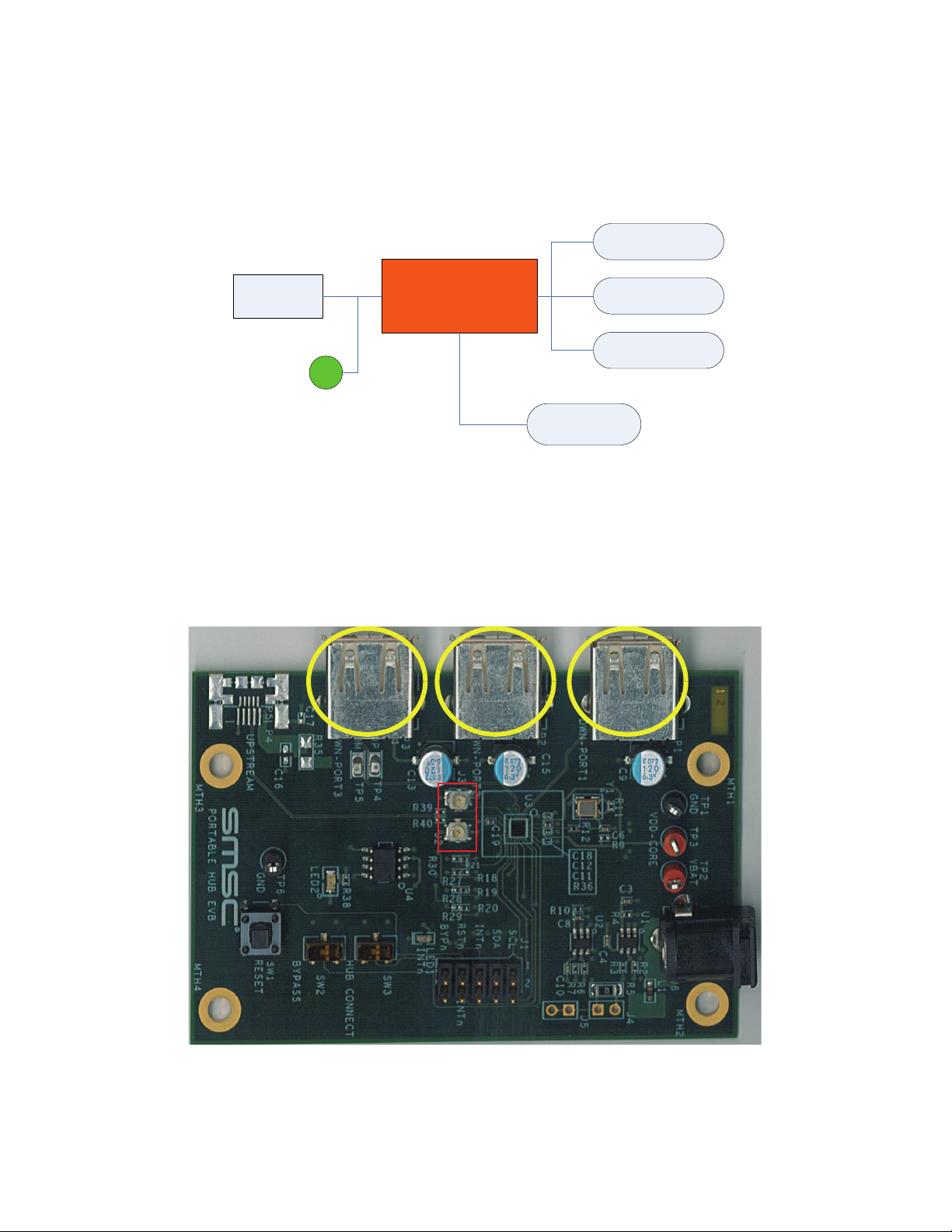
The downstream USB ports are mounted on the edges of the USB3503 EVB. The downstream ports
use the standard USB Type A receptacle. The label for the port is located near the receptacle. The
HSIC upstream port uses U.FL connectors for Data and Strobe.
Figure 3.2 Upstream and Downstream Ports
SMSC USB3503 EVB 3 Revision 1.0 (05-06-13)
USER MANUAL
Page 4
USB3503 EVB - Evaluation Board User Manual
TP2
TP1
J 1
Pin1
LED1
HUB_CONNECT
RESET
TP3
TP6
NOT USED
3.2 Test Points, Switches and LEDs
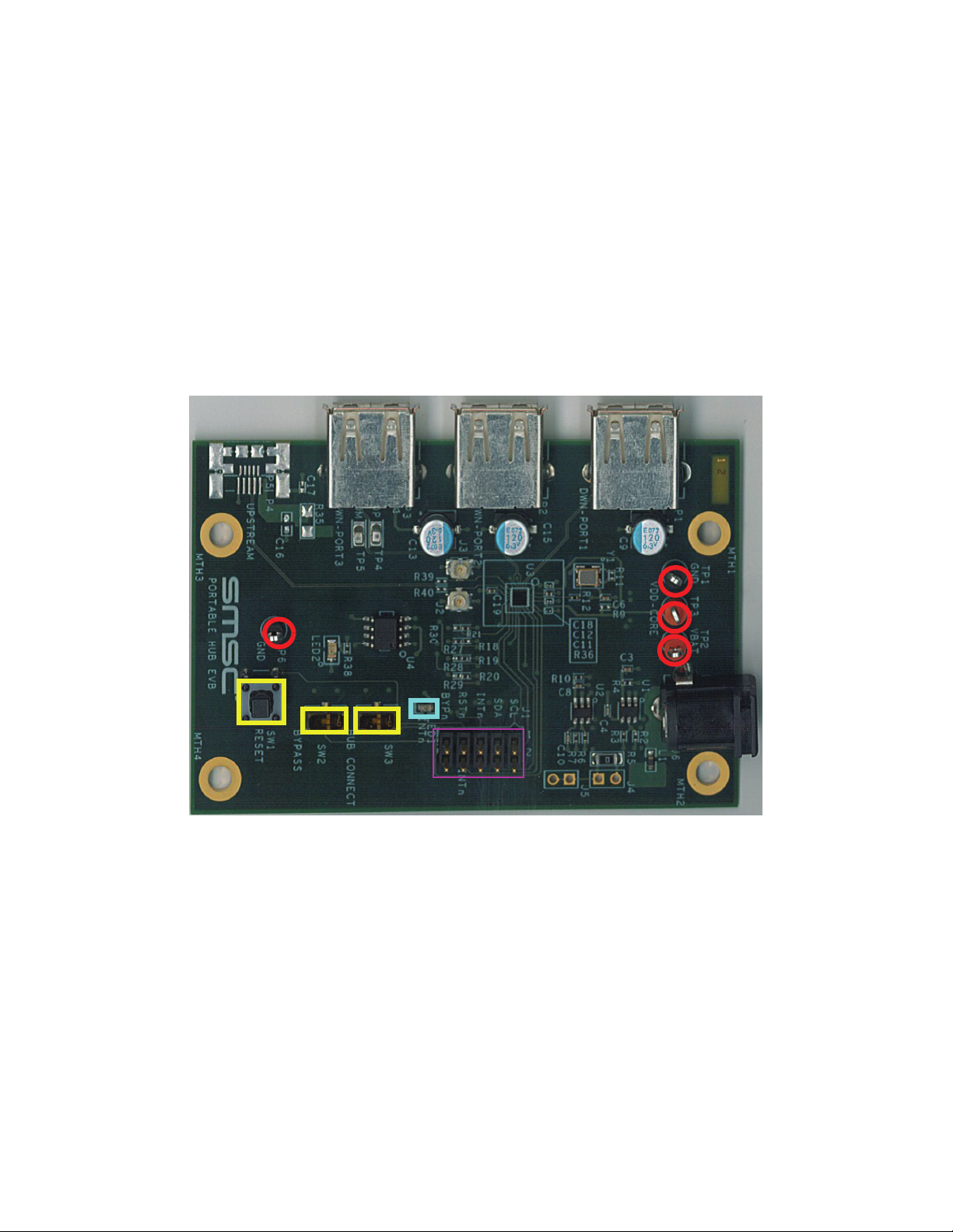
There are multiple test points to confirm that the USB3503 EVB is powered properly. TP1 and TP6
connect to GND, TP2 connects to the VBAT pin, and TP3 connects to the VDD_CORE_REG pin.
The USB3503 EVB also has three switches to manually control the RESET_N and HUB_CONNECT
inputs to the part. Figure 3.3 shows the location of the test points (Red) and switches (Yellow).
The USB3503 SCL, SDA, RESET_N, HUB_CONNECT and INT_B pins are also exposed on the J1
header. These pins are compatible with the Total Phase Aardvark pinout, where pin 1 of the Aardvark
connector connects to pin 1 of header J1 (Refer to Figure 4.1 for the proper way to connect the
Aardvark). The INT_N pin is also connected to LED1 to indicate that an interrupt has occurred. The
LED remains lit until the interrupt is cleared, as described in the USB3503 datasheet.
Figure 3.3 Test points, Switches, Header and LED
3.3 Configuration Resistors
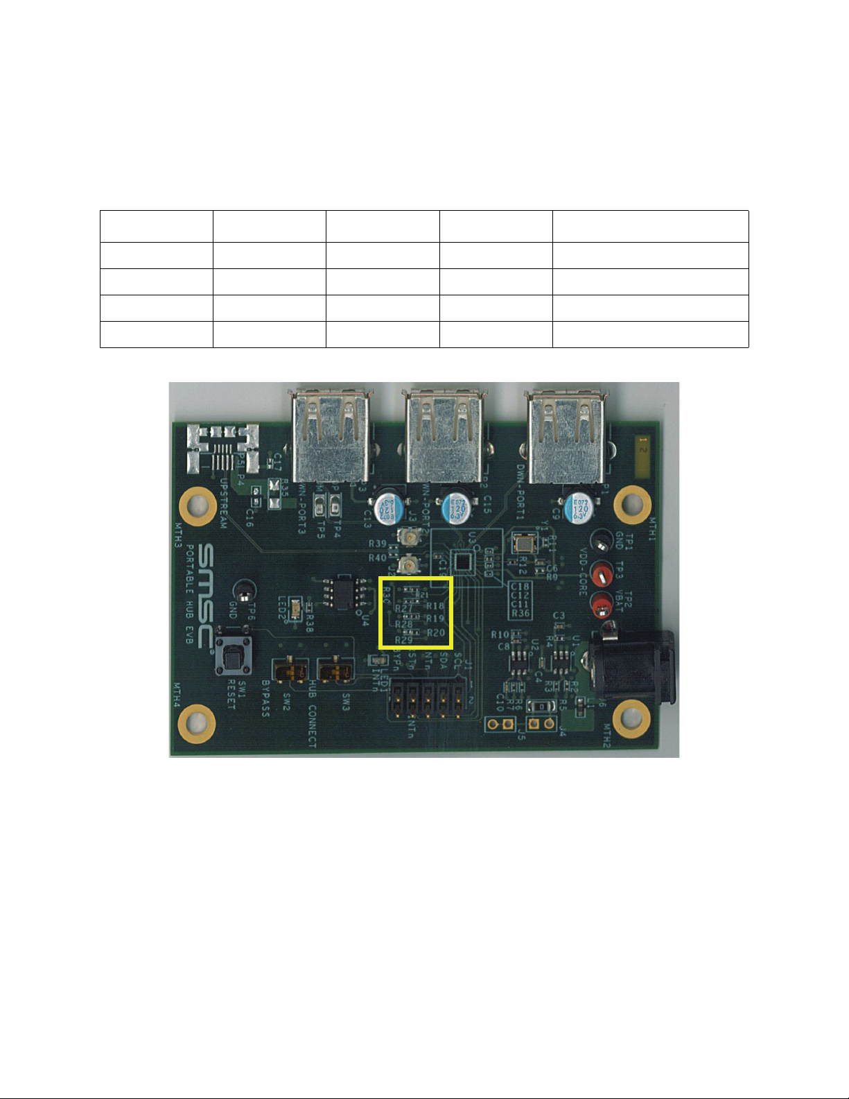
There are eight different resistors used to configure the part when the RESET_N pin transitions from
Low (0V) to High(>1.25V). These resistors are used for the REF_SEL pins. Because these resistors
and pads pull up to the 1.8V regulator, any changes to these resistors will need to be done with the
board unpowered. The resistor pads are laid out in a manner that prevents the pull-up resistors from
being populated at the same time as the pull-down resistors, as shown in Figure 3.4. The following
tables show the proper configuration resistor population requirements for the desired results, the
resistor values should match those found in Section 6, "USB3503 EVB Bill of Materials".
Revision 1.0 (05-06-13) 4 SMSC USB3503 EVB
USER MANUAL
Page 5
USB3503 EVB - Evaluation Board User Manual
Note: The Y1 Oscillator will need to be replaced with the proper frequency if the REF_SEL pins are
altered. Refer to Section 6, "USB3503 EVB Bill of Materials" for recommended oscillator
specifications.
Table 3.1 REF_SEL Options
R18R21R27R30 REFCLK(MHZ)
EMPTY EMPTY INSTALL INSTALL 38.4
EMPTY INSTALL INSTALL EMPTY 26.0 (Default)
INSTALL EMPTY EMPTY INSTALL 19.2
INSTALL INSTALL EMPTY EMPTY 12.0
Figure 3.4 Configuration Resistors
3.4 Additional Circuitry
The U1 Regulator provides 3.3V to the VBAT pin, and also supplies power to the 26MHz clock
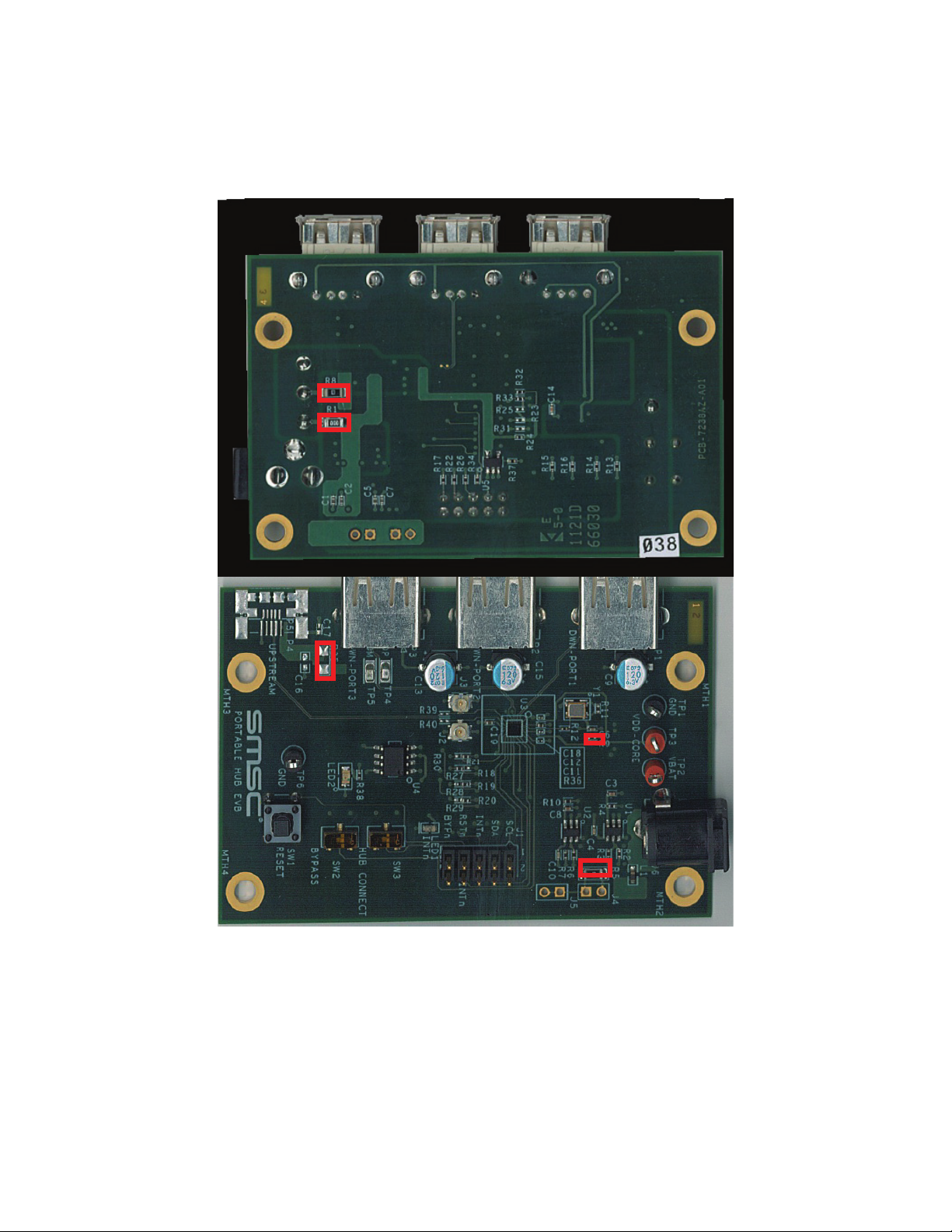
oscillator. If a higher VBAT voltage is desired, remove R1 and supply the power through TP2.
The U2 Regulator provides 1.8V to the VDD_CORE_REG pin as well as providing the pull up voltage
for the digital control pins. To provide external power to the VDD_CORE_REG pin remove R8 and
supply the power through TP3.
The USB3503 can function with a single power supply; to do this remove R8 and place a 0Ohm
resistor on R9. This connects the VDD_CORE_REG pin to the VDD33_BYP pin allowing the
USB3503’s internal 3.3V regulator to supply the VDD_CORE_REG voltage.
SMSC USB3503 EVB 5 Revision 1.0 (05-06-13)
USER MANUAL
Page 6

USB3503 EVB - Evaluation Board User Manual
Below is a summary of the different power options and what resistors need to be populated to support
these options:
Table 3.2 VBAT and VDD_CORE_REG Source Control
R1 R8 R9 VBAT SOURCE VDD_CORE_REG SOURCE
INSTALL INSTALL EMPTY Onboard Regulator Onboard Regulator
EMPTY INSTALL EMPTY External (TP2) Onboard Regulator
EMPTY EMPTY EMPTY External (TP2) External (TP3)
INSTALL EMPTY INSTALL Onboard Regulator VDD33_BYP
EMPTY EMPTY INSTALL External (TP2) VDD33_BYP
Revision 1.0 (05-06-13) 6 SMSC USB3503 EVB
USER MANUAL
Page 7
USB3503 EVB - Evaluation Board User Manual
R1
R8
R5
R9
R35
Below are the locations of the resistors on the back side of the board:
Figure 3.5 Regulator Resistors
SMSC USB3503 EVB 7 Revision 1.0 (05-06-13)
USER MANUAL
Page 8
USB3503 EVB - Evaluation Board User Manual
4 Software
The USB3503 EVB comes with a CD that contains evaluation software that can be used with the Total
Phase Aardvark USB-I
Setup.exe, found on the CD. This will install the USB3503 Evaluation Software, the LabVIEW Runtime engine (to run the executable), and the Total Phase drivers to communicate with the Aardvark.
Once the software has been installed, locate and run the USB3503 Evaluation.exe program on the
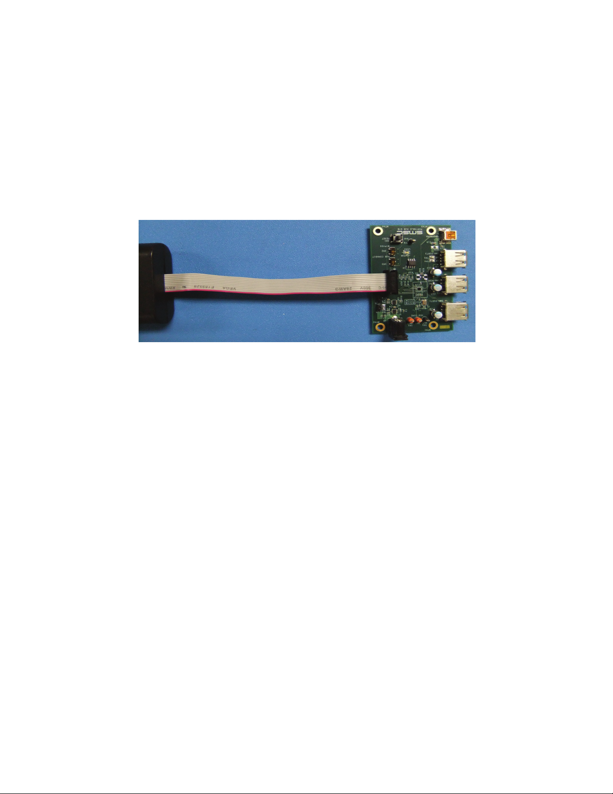
computer. Connect the Aardvark to the USB3503 EVB with the red wire facing the power port, as in
Figure 4.1.
2
C adaptor (not included with the Evaluation Kit). To install the software, run
Figure 4.1 Aardvark Connection
Revision 1.0 (05-06-13) 8 SMSC USB3503 EVB
USER MANUAL
Page 9
USB3503 EVB - Evaluation Board User Manual
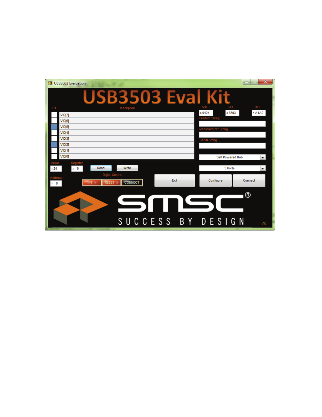
The software allows the user to control the digital input pins RESET_N and CONNECT. It also can
monitor the INT_N pin for interrupts. There is a section to communicate with the I2C serial port, as well
as some quick configuration and customization options.
Figure 4.2 USB3503 Evaluation Screen
4.1 Digital Control
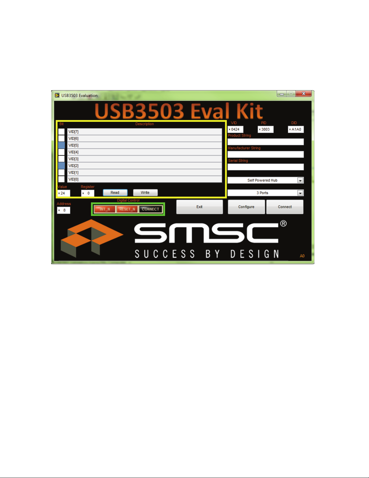
The RESET_N and HUB_CONNECT pins can be controlled in real time with the Digital Control array.
Each button in the array corresponds to the pin with the matching name. When the button is orange,
the pin is at logic level High. When the button is black the voltage is a logic level Low. Refer to the
green box in Figure 4.3 for the digital control array location.
Set the RESET_N pin low to reset the part and place it into the lowest power state. If the CONNECT
pin is low when the RESET pin transitions from low to high, the USB3503 will remain in a state that
allows the serial interface registers to be manipulated. To enumerate the hub, either write 00h to
register E7h, or drive the CONNECT pin high by pressing the CONNECT button in the Digital Control.
Once the USB3503 has enumerated, the serial interface registers should not be modified.
SMSC USB3503 EVB 9 Revision 1.0 (05-06-13)
USER MANUAL
Page 10
USB3503 EVB - Evaluation Board User Manual
Notes: To prevent the Aardvark from driving against another voltage, the Aardvark is running in an
Open/Drain mode, therefore it is important that all switches on the board pull the pins up to
the Vcc value.
2
Figure 4.3 Digital Control (Green) and I
C (Yellow) Sections
4.2 I2C Communication
The application also contains a general I2C register read/write section. The Bit and Description
display the serial interface register descriptions found in the USB3503 datasheet. The Register display
can be used to select the proper serial interface register to manipulate. Click on the Value or Bit box
above to change the value of the register. Once the desired value and register are selected, press the
Write button to change the value on the part. Click on the Read button and the Value and Bit boxes
will update the current value on the part. Refer to the USB3503 datasheet for a detailed description of
each register and operation of the device
4.3 Quick Configuration and Customization
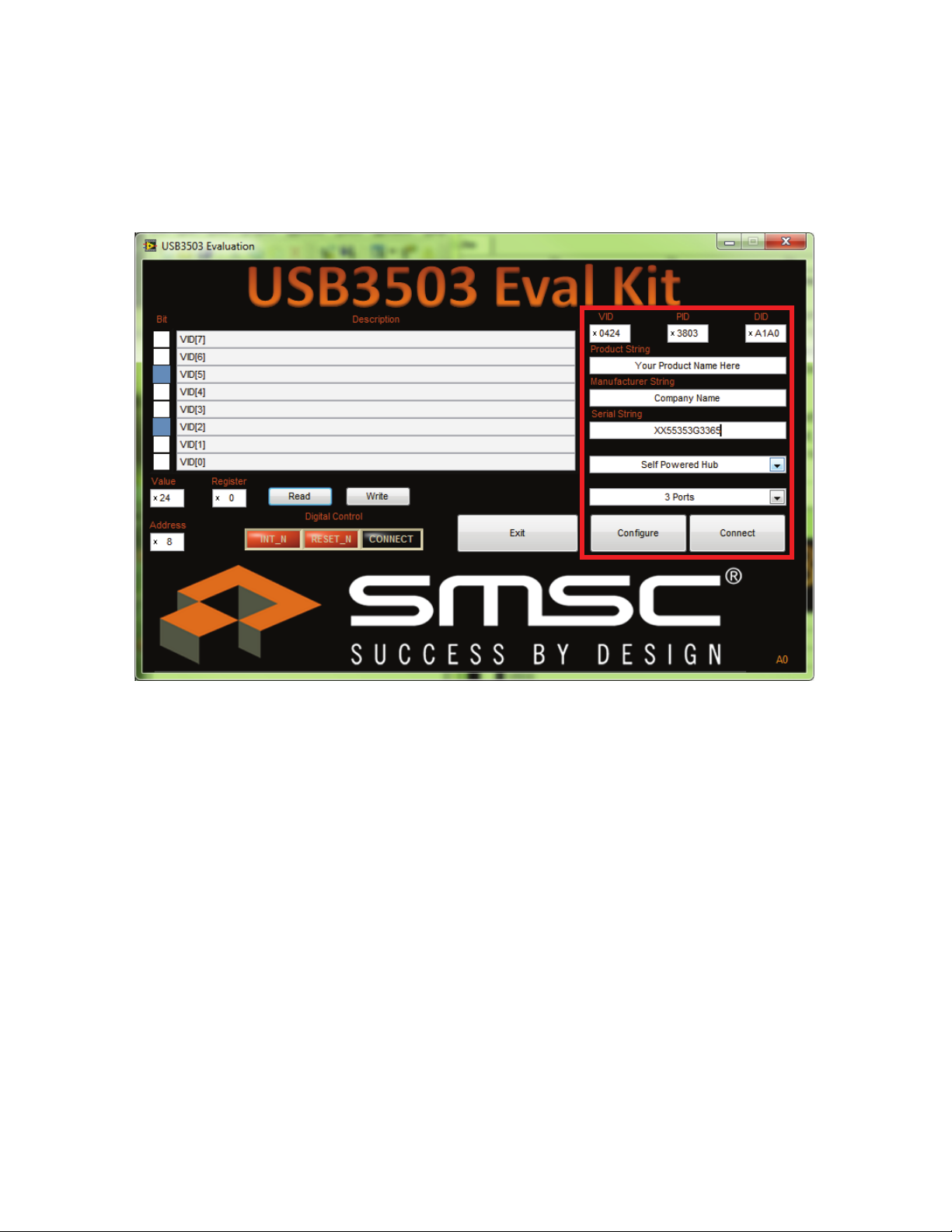
The USB3503 Evaluation program also contains some quick configuration and customization options
that automatically update the registers to match the desired configuration. The USB3503 can
enumerate as a Self Powered or Bus Powered Hub with 1, 2 or 3 downstream ports. The VID, PID,
DID and enumeration strings can also be customized to allow the USB3503 to enumerate with
whatever identification is desired.
Revision 1.0 (05-06-13) 10 SMSC USB3503 EVB
USER MANUAL
Page 11
USB3503 EVB - Evaluation Board User Manual
To change these values; update the configuration section to the desired options, then press the
Configure button. The part will then reset, pull the CONNECT pin low and update the registers as
specified. To go with these options either raise the CONNECT pin, or press the Connect button.
Figure 4.4 Quick Configuration Options
SMSC USB3503 EVB 11 Revision 1.0 (05-06-13)
USER MANUAL
Page 12
USB3503 EVB - Evaluation Board User Manual
5
5
4
4
3
3
2
2
1
1
D D
C C
B B
A A
USB3503 25-pin WLCSP Evaluation Board
DNP
DNP
DNPDNP
USB Connectors
3.3V VBAT (200mA)
1.8V VCC_CORE (200mA)
DNP
Digital Control
DNP
DNP
DNP
DNP
DNP
DNP
DNP
DNP
DNP
DNP
OCS_N
PORT_PWR
DN1_DP
VDD_CORE
VDD33_BYP
DN2_DP
DN1_DM
DN2_DM
VBUS
DN3_DP
DN3_DM
VBAT
VDD33_BYP
VDD_CORE
VBUS
PORT_PWR
OCS_N
PORT_PWR
STROBE
DATA
VDD_PU
5V
VBAT
5V VBAT
VBAT
VDD_PU
OSC
OSC
VDD_PU
Title
Size Document Number Rev
Date: Sheet
of
3930 East Ray Road
Suite 200
Phoenix, Arizona 85044
480-759-0200
SCH-7238AZ-A12 A
PCB7238: USB3503 Evaluation Board
B
11Monday, August 08, 2011
Title
Size Document Number Rev
Date: Sheet
of
3930 East Ray Road
Suite 200
Phoenix, Arizona 85044
480-759-0200
SCH-7238AZ-A12 A
PCB7238: USB3503 Evaluation Board
B
11Monday, August 08, 2011
Title
Size Document Number Rev
Date: Sheet
of
3930 East Ray Road
Suite 200
Phoenix, Arizona 85044
480-759-0200
SCH-7238AZ-A12 A
PCB7238: USB3503 Evaluation Board
B
11Monday, August 08, 2011
TP3
Orange
TP3
Orange
R/ANGLE USB A CON
P1
USB-A
R/ANGLE USB A CON
P1
USB-A
VCC1D-2D+3SHLD1
5
GND4SHLD2
6
P5
USB MICRO-AB
P5
USB MICRO-AB
VBUS1D-2D+3ID4GND5SHLD16SHLD27SHLD38SHLD49SHLD510SHLD6
11
SW3SW3
123
R25
ZERO
R25
ZERO
R16
10k
R16
10k
R1
ZEROR1ZERO
R3
30.1kR330.1k
R14
10k
R14
10k
C4
0.01uFC40.01uF
TP5TP5
+
C13
120uF
6.3V+C13
120uF
6.3V
R21
10k
R21
10k
R171kR17
1k
U2
TPS79301U2TPS79301
IN1GND2ENA
3
BYP
4
OUT
6
FB
5
R/ANGLE USB A CON
P3
USB-A
R/ANGLE USB A CON
P3
USB-A
VCC1D-2D+3SHLD1
5
GND4SHLD2
6
+
C9
120uF
6.3V+C9
120uF
6.3V
C3
0.1uFC30.1uF
R23
10k
R23
10k
L1
F-BEADL1F-BEAD
LED2
GREEN
LED2
GREEN
12
TP1
Black
TP1
Black
MOM-ON
SW1
MOM-ON
SW1
3
1
2
4
C19
1.0uF
C19
1.0uF
R35
ZERO
R35
ZERO
U3
USB3503_25WLCSP
U3
USB3503_25WLCSP
OCS_N
B4
INT_N
C5
PORT_PWR
C4
SDA
D5
REF_SEL1
D4
SCL
E5
REF_SEL0
E4
RESET_N
E3
VDD12_BYP
D3
DATA
E2
VSS
C3
REFCLK
B3
USBDN2_DMD2USBDN3_DM
D1
USBDN2_DP
C2
STROBE
E1
USBDN3_DP
C1
USBDN1_DP
A1
USBDN1_DM
B1
VDD33_BYP
A2
VDD33
A5
VBAT
B2
VDD_CORE_REG
A3
RBIAS
A4
HUB_CONNECT
B5
MTH4MTH4
MH
1
C7
18pFC718pF
R33
ZERO
R33
ZERO
C14
0.1uF
C14
0.1uF
R18
10k
R18
10k
R8
ZEROR8ZERO
R36
12.0k
R36
12.0k
J6
Power_JackJ6Power_Jack
132
U4
MIC2026-1BU4MIC2026-1B
IN
7
ENA
1
OUTA8OUTB
5
FLAGA
2
ENB4GND
6
FLAGB
3
R31
ZERO
R31
ZERO
R6
14.3kR614.3k
R5
ZEROR5ZERO
C5
4.7uFC54.7uF
R381kR38
1k
C10
0.01uF
C10
0.01uF
P4USB mini AB SMD P4USB mini AB SMD
VBUS1D+3D-2ID4GND5SHIELD16SHIELD27SHIELD38SHIELD4
9
R12
ZERO
R12
ZERO
J3J3
132
J4J4
1 2
R32
ZERO
R32
ZERO
R221kR22
1k
MTH1MTH1
MH
1
R2
51.0kR251.0k
R39
ZERO
R39
ZERO
R11
10k
R11
10k
C18
0.1uF
C18
0.1uF
C12
4.7µF
C12
4.7µF
R20
10k
R20
10k
R13
10k
R13
10k
TP4TP4
R37
330
R37
330
C17
0.1uF
C17
0.1uF
C6
0.1uFC60.1uF
C8
0.1uFC80.1uF
R4
10kR410k
R15
10k
R15
10k
TP2
Orange
TP2
Orange
R28
10k
R28
10k
MTH3MTH3
MH
1
R34
10k
R34
10k
R/ANGLE USB A CON
P2
USB-A
R/ANGLE USB A CON
P2
USB-A
VCC1D-2D+3SHLD1
5
GND4SHLD2
6
R30
10k
R30
10k
R29
10k
R29
10k
R27
10k
R27
10k
C1
4.7uFC14.7uF
SW2SW2
123
Y1
26.0 MHz
3.3VY126.0 MHz
3.3V
VCC
4
OUT
3
EN1GND
2
R9
ZEROR9ZERO
+
C15
120uF
6.3V+C15
120uF
6.3V
R7
30.1kR730.1k
U1
TPS79301U1TPS79301
IN1GND2ENA
3
BYP
4
OUT
6
FB
5
R24
10k
R24
10k
U5
SCHMITT TRIG
U5
SCHMITT TRIG
24
53
1
MTH2MTH2
MH
1
R19
10k
R19
10k
R10
10k
R10
10k
J5J5
1 2
J2J2
132
LED1
Green
LED1
Green
12
J1J1
1
3425678910
C2
18pFC218pF
R40
ZERO
R40
ZERO
R26
10k
R26
10k
C16
4.7uF
C16
4.7uF
C11
0.1uF
C11
0.1uF
TP6
Black
TP6
Black
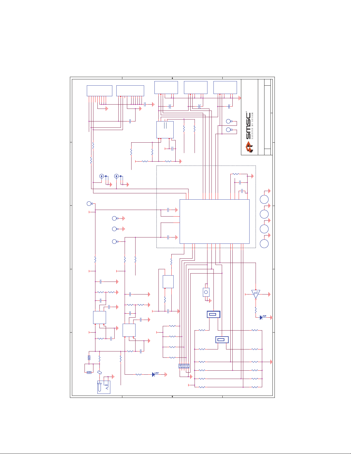
5 USB3503 EVB Schematic
Revision 1.0 (05-06-13) 12 SMSC USB3503 EVB
Figure 5.1 USB3503 EVB Schematic
USER MANUAL
Page 13
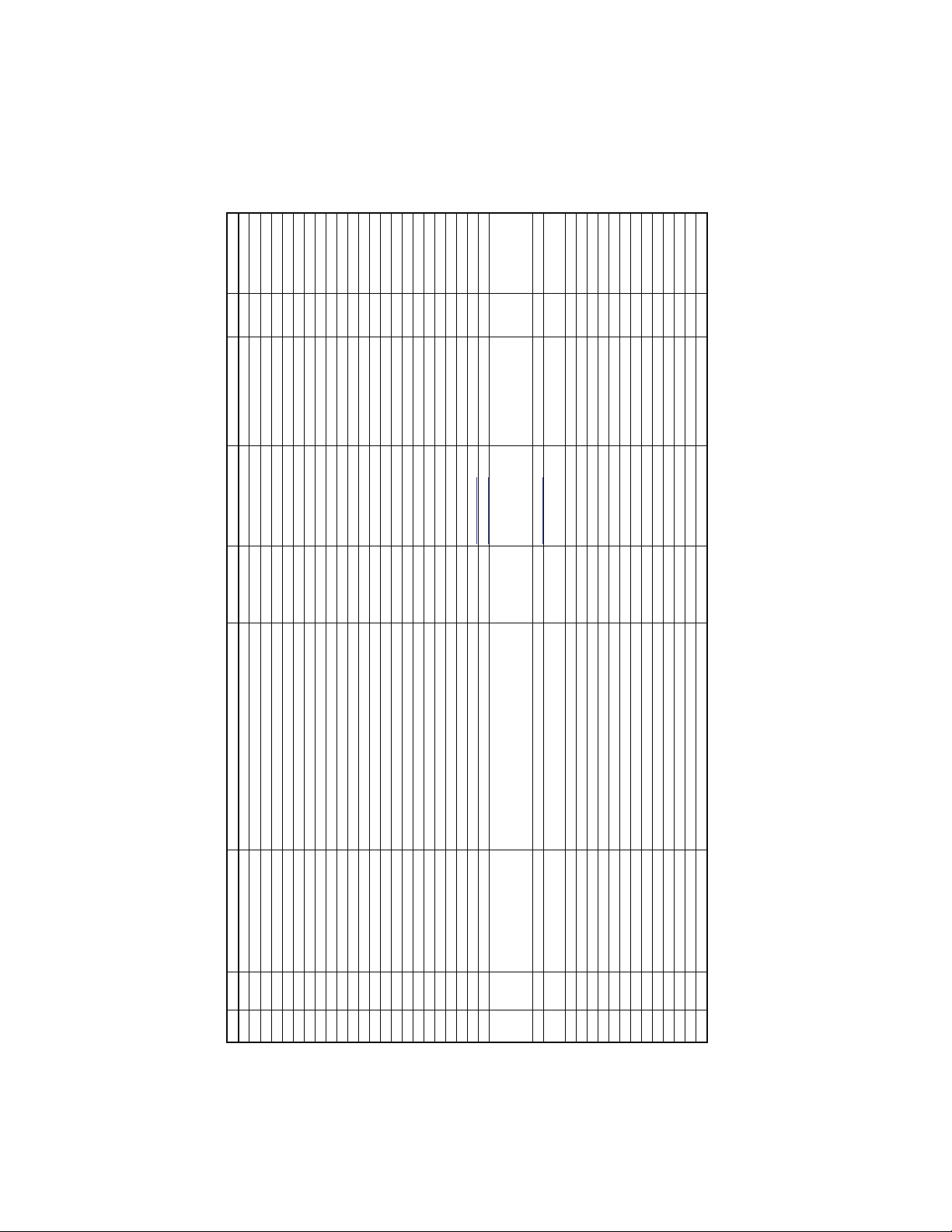
6 USB3503 EVB Bill of Materials
Part ID Quantity
Part Reference
Description Digikey_Number Manuf Manuf_PN RoHS
DNP
1 2 C1 C5 CAPACITOR CERAMIC 4.7UF 10V X5R 0603 587-1441-1-ND TAIYO YUDEN LMK107BJ475KA-T Yes
2 2 C2 C7 CAPACITOR CERAMIC 18PF 50V 0402 SMD PCC180CQCT-ND PANASONIC ECJ-0EC1H180J Yes
3 7 C3 C6 C8 C14 C17 CAPACITOR CERAMIC 0.1UF 10V X5R 0402 PCC2146CT-ND PANASONIC ECJ-0EB1A104K Yes C17
4 2 C4 C10 CAPACITOR CERAMIC 0.01UF 16V 10% X7R 060 PCC1750CT-ND PANASONIC ECJ-1VB1C103K Yes
5 2 C11 C18 CAPACITOR CERAMIC 0.1UF 10V X5R 0201 PCC2424CT-ND PANASONIC ECJ-ZEB1A104M Yes
6 3 C9 C13 C15 CAP 120UF 6.3V ELECT POLY SMD 565-3188-1-ND United Chemi-Con APXE6R3ARA121ME61G Yes
7 1 C12 CAPACITOR CERAMIC 4.7UF 6.3V X5R 0402 490-5408-1-ND MURATA ERIE GRM155R60J475ME87D Yes
81C16 CAPACITOR CERAMIC 4.7UF 6.3V X5R 20% 0603 445-1417-1-ND TDK C1608X5R0J475M Yes C16
9 1 C19 CAPACITOR CERAMIC 1.0UF 6.3V 20% X5R 0402 490-1319-1-ND MURATA ERIE GRM155R60J105ME19D Yes
10 1 J1 HEADER, 2 X 5, 0.1 INCH, VERTICAL SAM1030-05-ND SAMTEC TSW-105-07-L-D Yes
11 J2 J3 CONN RECPT U.FL H9161CT-ND HIROSE U.FL-R-SMT (10) Yes
12 2 J4 J5 HEADER, 1 X 2, 0.1 INCH, VERTICAL WM6402-ND MOLEX 22-28-4020 Yes J4 J5
13 1 J6 CONNECTOR POWER JACK 2.1X5.5MM HIGH CURR CP-002AH-ND CUI STACK PJ-002AH Yes
14 1 L1 FERRITE BEAD, 120 OHM, 0.5A, 0.1DCR, 0603 P10750CT-ND PANASONIC EXC-3BP121H Yes
15 1 LED1 LED GREEN SMT 404-1005-1-ND STANLEY BG1111C-TR Yes
16 1 LED2 LED GREEN 2X1.2MM 568NM GN WTR CLR SMD 754-1131-1-ND Kingbright APT2012SGC Yes
17 4 MTH1 MTH2 MTH3 MTH4 MOUNTING PAD MTG250C140D
18 3 P1 P2 P3 RECEPTACLE, USB, STYLE B, RIGHT ANGLE 609-1045-ND FCI 87520-0010BLF Yes
19 1 P4 CONNECTOR RECEPT USB MINI AB 5POS RT ANG WM17122CT-ND MOLEX 56579-0576 Yes P4
20 0 P5 CONNECTOR RECEPT MICRO USB TYPE AB SMT A97799CT-ND TYCO ELECTRONICS 1981584-1 Yes P5
21 2 R1 R5 R8 R35 RESISTOR ZERO OHM 1/4W 5% 1206 311-0.0ERCT-ND YAGEO RC1206JR-070RL Yes R35
22 1 R2 RES 51.0K OHM 1/10W 1% 0402 SMD P51.0KLCT-ND Panasonic - ECG
ERJ-2RKF5102X Yes
23 2 R3 R7 RES 30.1K OHM 1/10W 1% 0402 SMD P30.1KLCT-ND Panasonic - ECG
ERJ-2RKF3012X Yes
24 15
R4 R10 R11 R13 R14 R15
R16 R18 R19 R20 R21 R23
R24 R26 R27 R28 R29 R30
R34
RESISTOR 10K OHM 1/16W 5% 0402 SMD P10KJCT-ND PANASONIC ERJ-2GEJ103X Yes
R18 R23 R28 R29
R30
25 1 R6 RES 14.3K OHM 1/10W 1% 0402 SMD P14.3KLCT-ND Panasonic - ECG
ERJ-2RKF1432X Yes
26 4
R9 R12 R25 R31 R32 R33
R39 R40
RESISTOR ZERO OHM 1/16W 5% 0402 SMD 311-0.0JRCT-ND YAGEO RC0402JR-070RL Yes
R9 R25 R32 R39
R40
27 3 R17 R22 R38 RESISTOR 1.0K OHM 1/16W 5% 0402 SMD P1.0KJCT-ND PANASONIC ERJ-2GEJ102X Yes
28 1 R36 RESISTOR 12.0K OHM 1/20W 1% 0201 SMD P12.0KABCT-ND PANASONIC ERJ-1GEF1202C Yes
29 1 R37 RESISTOR 330 OHM 1/16W 1% 0402 SMD 311-330LRCT-ND YAGEO RC0402FR-07330RL Yes
30 1 SW1 SWITCH TACTILE 6MM EXTEND ACT 160GF EG1861-ND E-SWITCH TL1105SPF160Q Yes
31 2 SW2 SW3 SWITCH SLIDE SPDT SMD GULL 563-1022-1-ND COPAL ELECTRONICS CJS-1200TB Yes
32 2 TP1 TP6 TEST POINT LOOP COMPACT BLACK 5006K-ND KEYSTONE 5006 Yes
33 2 TP2 TP3 TEST POINT LOOP COMPACT ORANGE 5008K-ND KEYSTONE 5008 Yes
34 2 TP4 TP5 TEST POINT 5015KCT-ND KEYSTONE 5015 Yes
35 2 U1 U2 IC 200MA LDO LINEAR REG SOT23-6 296-15305-1-ND TEXAS INSTRUMENTS TPS79301DBVRQ1 Yes
36 1 U3 USB3503_25WLCSP SMSC USB3503 Yes
37 1 U4 POWER SWITCH USB MIC2026-1B 576-2137-ND MICREL MIC2026-1YM Yes
38 1 U5 IC SCHMITT-TRG INV GATE SOT23-5 296-1092-1-ND TEXAS INSTRUMENTS SN74AHC1G14DBVR Yes
39 1 Y1 OSCILLATOR PROG 3.3V +-50PPM SMD AP3S3EC-ND ABRACON AP3S-26.0MHz Yes
USB3503 EVB - Evaluation Board User Manual
Figure 6.1 USB3503 EVB Bill of Materials
SMSC USB3503 EVB 13 Revision 1.0 (05-06-13)
USER MANUAL
Page 14

USB3503 EVB - Evaluation Board User Manual
7 User Manual Revision History
Table 7.1 Customer Revision History
REVISION LEVEL & DATE SECTION/FIGURE/ENTRY CORRECTION
Rev. 1.0 (05-06-13) Co-branded document
Rev. 1.0 (09-12-11) Document release
Revision 1.0 (05-06-13) 14 SMSC USB3503 EVB
USER MANUAL
 Loading...