

Page 1

LAN9514
USB Hub with Integrated
10/100 Ethernet Controller
PRODUCT FEATURES
Highlights
Four downstream ports, one upstream port
— Four integrated downstream USB 2.0 PHYs
— One integrated upstream USB 2.0 PHY
Integrated 10/100 Ethernet MAC with full-duplex
support
Integrated 10/100 Ethernet PHY with HP Auto-MDIX
Implements Reduced Power Operating Modes
Minimized BOM Cost
— Single 25 MHz crystal (Eliminates cost of separate
crystals for USB and Ethernet)
— Built-in Power-On-Reset (POR) circuit (Eliminates
requirement for external passive or active reset)
Target Applications
Desktop PCs
Notebook PCs
Printers
Game Consoles
Embedded Systems
Docking Stations
Key Benefits
USB Hub
— Fully compliant with Universal Serial Bus Specification
Revision 2.0
— HS (480 Mbps), FS (12 Mbps), and LS (1.5 Mbps)
compatible
— Four downstream ports, one upstream port
— Port mapping and disable support
— Port Swap: Programmable USB diff-pair pin location
— PHY Boost: Programmable USB signal drive strength
— Select presence of a permanently hardwired USB
peripheral device on a port by port basis
— Advanced power saving features
— Downstream PHY goes into low power mode when port
power to the port is disabled
— Full Power Management with individual or ganged
power control of each downstream port.
— Integrated USB termination Pull-up/Pull-down resistors
— Internal short circuit protection of USB differential signal
pins
SMSC LAN9514 Revision 1.0 (04-20-09)
High-Performance 10/100 Ethernet Controller
— Fully compliant with IEEE802.3/802.3u
— Integrated Ethernet MAC and PHY
— 10BASE-T and 100BASE-TX support
— Full- and half-duplex support with flow control
— Preamble generation and removal
— Automatic 32-bit CRC generation and checking
— Automatic payload padding and pad removal
— Loop-back modes
— TCP/UDP checksum offload support
— Flexible address filtering modes
– One 48-bit perfect address
– 64 hash-filtered multicast addresses
– Pass all multicast
– Promiscuous mode
– Inverse filtering
– Pass all incoming with status report
— Wakeup packet support
— Integrated Ethernet PHY
– Auto-negotiation
– Automatic polarity detection and correction
– HP Auto-MDIX
– Energy Detect
Power and I/Os
— Three PHY LEDs
— Eight GPIOs
— Supports bus-powered and self-powered operation
— Internal 1.8v core supply regulator
— External 3.3v I/O supply
Miscellaneous features
— Optional EEPROM
— Optional 24MHz reference clock output for partner hub
— IEEE 1149.1 (JTAG) Boundary Scan
Software
— Windows 2000/XP/Vista Driver
— Linux Driver
— Win CE Driver
—MAC OS Driver
— EEPROM Utility
Packaging
— 64-pin QFN, lead-free RoHS compliant
Environmental
— Commercial Temperature Range (0°C to +70°C)
— ±8kV HBM without External Protection Devices
— ±8kV contact mode (IEC61000-4-2)
— ±15kV air-gap discharge mode (IEC61000-4-2)
Datasheet
DATASHEET
Page 2

USB Hub with Integrated 10/100 Ethernet Controller
Datasheet
ORDER NUMBERS:
LAN9514-JZX FOR 64-PIN, QFN LEAD-FREE ROHS COMPLIANT PACKAGE (0 TO +70°C TEMP RANGE)
80 ARKAY DRIVE, HAUPPAUGE, NY 11788 (631) 435-6000, FAX (631) 273-3123
Copyright © 2009 SMSC or its subsidiaries. All rights reserved.
Circuit diagrams and other information relating to SMSC products are included as a means of illustrating typical applications. Consequently, complete information sufficient for
construction purposes is not necessarily given. Although the information has been checked and is believed to be accurate, no responsibility is assumed for inaccuracies. SMSC
reserves the right to make changes to specifications and product descriptions at any time without notice. Contact your local SMSC sales office to obtain the latest specifications
before placing your product order. The provision of this information does not convey to the purchaser of the described semiconductor devices any licenses under any patent
rights or other intellectual property rights of SMSC or others. All sales are expressly conditional on your agreement to the terms and conditions of the most recently dated
version of SMSC's standard Terms of Sale Agreement dated before the date of your order (the "Terms of Sale Agreement"). The product may contain design defects or errors
known as anomalies which may cause the product's functions to deviate from published specifications. Anomaly sheets are available upon request. SMSC products are not
designed, intended, authorized or warranted for use in any life support or other application where product failure could cause or contribute to personal injury or severe property
damage. Any and all such uses without prior written approval of an Officer of SMSC and further testing and/or modification will be fully at the risk of the customer. Copies of
this document or other SMSC literature, as well as the Terms of Sale Agreement, may be obtained by visiting SMSC’s website at http://www.smsc.com. SMSC is a registered
trademark of Standard Microsystems Corporation (“SMSC”). Product names and company names are the trademarks of their respective holders.
SMSC DISCLAIMS AND EXCLUDES ANY AND ALL WARRANTIES, INCLUDING WITHOUT LIMITATION ANY AND ALL IMPLIED WARRANTIES OF MERCHANTABILITY,
FITNESS FOR A PARTICULAR PURPOSE, TITLE, AND AGAINST INFRINGEMENT AND THE LIKE, AND ANY AND ALL WARRANTIES ARISING FROM ANY COURSE
OF DEALING OR USAGE OF TRADE. IN NO EVENT SHALL SMSC BE LIABLE FOR ANY DIRECT, INCIDENTAL, INDIRECT, SPECIAL, PUNITIVE, OR CONSEQUENTIAL
DAMAGES; OR FOR LOST DATA, PROFITS, SAVINGS OR REVENUES OF ANY KIND; REGARDLESS OF THE FORM OF ACTION, WHETHER BASED ON CONTRACT;
TORT; NEGLIGENCE OF SMSC OR OTHERS; STRICT LIABILITY; BREACH OF WARRANTY; OR OTHERWISE; WHETHER OR NOT ANY REMEDY OF BUYER IS HELD
TO HAVE FAILED OF ITS ESSENTIAL PURPOSE, AND WHETHER OR NOT SMSC HAS BEEN ADVISED OF THE POSSIBILITY OF SUCH DAMAGES.
Revision 1.0 (04-20-09) 2 SMSC LAN9514
DATASHEET
Page 3

USB Hub with Integrated 10/100 Ethernet Controller
Datasheet
Table of Contents
Chapter 1 Introduction . . . . . . . . . . . . . . . . . . . . . . . . . . . . . . . . . . . . . . . . . . . . . . . . . . . . . . . 6
1.1 Block Diagram . . . . . . . . . . . . . . . . . . . . . . . . . . . . . . . . . . . . . . . . . . . . . . . . . . . . . . . . . . . . . . . . . 6
1.1.1 Overview . . . . . . . . . . . . . . . . . . . . . . . . . . . . . . . . . . . . . . . . . . . . . . . . . . . . . . . . . . . . . . 6
1.1.2 USB Hub . . . . . . . . . . . . . . . . . . . . . . . . . . . . . . . . . . . . . . . . . . . . . . . . . . . . . . . . . . . . . . 7
1.1.3 Ethernet Controller . . . . . . . . . . . . . . . . . . . . . . . . . . . . . . . . . . . . . . . . . . . . . . . . . . . . . . 7
1.1.4 EEPROM Controller . . . . . . . . . . . . . . . . . . . . . . . . . . . . . . . . . . . . . . . . . . . . . . . . . . . . . 7
1.1.5 Peripherals . . . . . . . . . . . . . . . . . . . . . . . . . . . . . . . . . . . . . . . . . . . . . . . . . . . . . . . . . . . . 7
1.1.6 Power Management . . . . . . . . . . . . . . . . . . . . . . . . . . . . . . . . . . . . . . . . . . . . . . . . . . . . . 7
Chapter 2 Pin Description and Configuration . . . . . . . . . . . . . . . . . . . . . . . . . . . . . . . . . . . . 9
2.1 Port Power Control . . . . . . . . . . . . . . . . . . . . . . . . . . . . . . . . . . . . . . . . . . . . . . . . . . . . . . . . . . . . . 16
2.1.1 Port Power Control Using a USB Power Switch . . . . . . . . . . . . . . . . . . . . . . . . . . . . . . . 16
2.1.2 Port Power Control Using a Poly Fuse . . . . . . . . . . . . . . . . . . . . . . . . . . . . . . . . . . . . . . 17
2.2 Buffer Types . . . . . . . . . . . . . . . . . . . . . . . . . . . . . . . . . . . . . . . . . . . . . . . . . . . . . . . . . . . . . . . . . . 19
Chapter 3 EEPROM Controller (EPC) . . . . . . . . . . . . . . . . . . . . . . . . . . . . . . . . . . . . . . . . . 20
3.1 EEPROM Format . . . . . . . . . . . . . . . . . . . . . . . . . . . . . . . . . . . . . . . . . . . . . . . . . . . . . . . . . . . . . . 20
3.1.1 Hub Configuration . . . . . . . . . . . . . . . . . . . . . . . . . . . . . . . . . . . . . . . . . . . . . . . . . . . . . . 23
3.2 EEPROM Defaults . . . . . . . . . . . . . . . . . . . . . . . . . . . . . . . . . . . . . . . . . . . . . . . . . . . . . . . . . . . . . 33
3.3 EEPROM Auto-Load. . . . . . . . . . . . . . . . . . . . . . . . . . . . . . . . . . . . . . . . . . . . . . . . . . . . . . . . . . . . 33
3.4 An Example of EEPROM Format Interpretation . . . . . . . . . . . . . . . . . . . . . . . . . . . . . . . . . . . . . . . 34
Chapter 4 Operational Characteristics . . . . . . . . . . . . . . . . . . . . . . . . . . . . . . . . . . . . . . . . . 39
4.1 Absolute Maximum Ratings*. . . . . . . . . . . . . . . . . . . . . . . . . . . . . . . . . . . . . . . . . . . . . . . . . . . . . . 39
4.2 Operating Conditions** . . . . . . . . . . . . . . . . . . . . . . . . . . . . . . . . . . . . . . . . . . . . . . . . . . . . . . . . . . 39
4.3 Power Consumption . . . . . . . . . . . . . . . . . . . . . . . . . . . . . . . . . . . . . . . . . . . . . . . . . . . . . . . . . . . . 40
4.3.1 Operational Current Consumption & Power Dissipation . . . . . . . . . . . . . . . . . . . . . . . . . 40
4.4 DC Specifications . . . . . . . . . . . . . . . . . . . . . . . . . . . . . . . . . . . . . . . . . . . . . . . . . . . . . . . . . . . . . . 41
4.5 AC Specifications . . . . . . . . . . . . . . . . . . . . . . . . . . . . . . . . . . . . . . . . . . . . . . . . . . . . . . . . . . . . . . 43
4.5.1 Equivalent Test Load . . . . . . . . . . . . . . . . . . . . . . . . . . . . . . . . . . . . . . . . . . . . . . . . . . . . 43
4.5.2 Reset Timing . . . . . . . . . . . . . . . . . . . . . . . . . . . . . . . . . . . . . . . . . . . . . . . . . . . . . . . . . . 43
4.5.3 EEPROM Timing . . . . . . . . . . . . . . . . . . . . . . . . . . . . . . . . . . . . . . . . . . . . . . . . . . . . . . . 44
4.6 Clock Circuit . . . . . . . . . . . . . . . . . . . . . . . . . . . . . . . . . . . . . . . . . . . . . . . . . . . . . . . . . . . . . . . . . . 45
Chapter 5 Package Outline . . . . . . . . . . . . . . . . . . . . . . . . . . . . . . . . . . . . . . . . . . . . . . . . . . . 46
5.1 64-QFN Package . . . . . . . . . . . . . . . . . . . . . . . . . . . . . . . . . . . . . . . . . . . . . . . . . . . . . . . . . . . . . . 46
SMSC LAN9514 3 Revision 1.0 (04-20-09)
DATASHEET
Page 4

USB Hub with Integrated 10/100 Ethernet Controller
Datasheet
List of Figures
Figure 1.1 Internal Block Diagram . . . . . . . . . . . . . . . . . . . . . . . . . . . . . . . . . . . . . . . . . . . . . . . . . . . . . . . 6
Figure 2.1 LAN9514 64-QFN Pin Assignments (TOP VIEW) . . . . . . . . . . . . . . . . . . . . . . . . . . . . . . . . . . 9
Figure 2.2 Port Power Control with USB Power Switch . . . . . . . . . . . . . . . . . . . . . . . . . . . . . . . . . . . . . 16
Figure 2.3 Port Power Control with Poly Fuse . . . . . . . . . . . . . . . . . . . . . . . . . . . . . . . . . . . . . . . . . . . . 17
Figure 2.4 Port Power with Ganged Control with Poly Fuse . . . . . . . . . . . . . . . . . . . . . . . . . . . . . . . . . . 18
Figure 4.1 Output Equivalent Test Load . . . . . . . . . . . . . . . . . . . . . . . . . . . . . . . . . . . . . . . . . . . . . . . . . 43
Figure 4.1 EEPROM Timing . . . . . . . . . . . . . . . . . . . . . . . . . . . . . . . . . . . . . . . . . . . . . . . . . . . . . . . . . . 44
Figure 5.1 LAN9514 64-QFN Package Definition . . . . . . . . . . . . . . . . . . . . . . . . . . . . . . . . . . . . . . . . . . 46
Figure 5.2 LAN9514 Recommended PCB Land Pattern. . . . . . . . . . . . . . . . . . . . . . . . . . . . . . . . . . . . . 47
Revision 1.0 (04-20-09) 4 SMSC LAN9514
DATASHEET
Page 5

USB Hub with Integrated 10/100 Ethernet Controller
Datasheet
List of Tables
Table 2.1 EEPROM Pins . . . . . . . . . . . . . . . . . . . . . . . . . . . . . . . . . . . . . . . . . . . . . . . . . . . . . . . . . . . . . 10
Table 2.2 JTAG Pins . . . . . . . . . . . . . . . . . . . . . . . . . . . . . . . . . . . . . . . . . . . . . . . . . . . . . . . . . . . . . . . . 10
Table 2.3 Miscellaneous Pins . . . . . . . . . . . . . . . . . . . . . . . . . . . . . . . . . . . . . . . . . . . . . . . . . . . . . . . . . 10
Table 2.4 USB Pins . . . . . . . . . . . . . . . . . . . . . . . . . . . . . . . . . . . . . . . . . . . . . . . . . . . . . . . . . . . . . . . . . 12
Table 2.5 Ethernet PHY Pins . . . . . . . . . . . . . . . . . . . . . . . . . . . . . . . . . . . . . . . . . . . . . . . . . . . . . . . . . . 14
Table 2.6 I/O Power Pins, Core Power Pins, and Ground Pad . . . . . . . . . . . . . . . . . . . . . . . . . . . . . . . . 14
Table 2.7 64-QFN Package Pin Assignments . . . . . . . . . . . . . . . . . . . . . . . . . . . . . . . . . . . . . . . . . . . . . 15
Table 2.8 Buffer Types . . . . . . . . . . . . . . . . . . . . . . . . . . . . . . . . . . . . . . . . . . . . . . . . . . . . . . . . . . . . . . 19
Table 3.1 EEPROM Format . . . . . . . . . . . . . . . . . . . . . . . . . . . . . . . . . . . . . . . . . . . . . . . . . . . . . . . . . . . 20
Table 3.2 Configuration Flags Description. . . . . . . . . . . . . . . . . . . . . . . . . . . . . . . . . . . . . . . . . . . . . . . . 22
Table 3.3 Hub Configuration . . . . . . . . . . . . . . . . . . . . . . . . . . . . . . . . . . . . . . . . . . . . . . . . . . . . . . . . . . 23
Table 3.4 Config Data Byte 1 Register (CFG1) Format . . . . . . . . . . . . . . . . . . . . . . . . . . . . . . . . . . . . . . 29
Table 3.5 Config Data Byte 2 Register (CFG2) Format . . . . . . . . . . . . . . . . . . . . . . . . . . . . . . . . . . . . . . 30
Table 3.6 Config Data Byte 3 Register (CFG3) Format . . . . . . . . . . . . . . . . . . . . . . . . . . . . . . . . . . . . . . 31
Table 3.7 Boost_Up Register (BOOSTUP) Format . . . . . . . . . . . . . . . . . . . . . . . . . . . . . . . . . . . . . . . . . 31
Table 3.8 Boost_5 Register (BOOST5) Format. . . . . . . . . . . . . . . . . . . . . . . . . . . . . . . . . . . . . . . . . . . . 31
Table 3.9 Boost_4:2 Register (BOOST42) Format . . . . . . . . . . . . . . . . . . . . . . . . . . . . . . . . . . . . . . . . . 32
Table 3.10 Status/Command Register (STCD) Format. . . . . . . . . . . . . . . . . . . . . . . . . . . . . . . . . . . . . . . 32
Table 3.11 EEPROM Defaults . . . . . . . . . . . . . . . . . . . . . . . . . . . . . . . . . . . . . . . . . . . . . . . . . . . . . . . . . . 33
Table 3.12 Dump of EEPROM Memory. . . . . . . . . . . . . . . . . . . . . . . . . . . . . . . . . . . . . . . . . . . . . . . . . . . 34
Table 3.13 EEPROM Example - 256 Byte EEPROM . . . . . . . . . . . . . . . . . . . . . . . . . . . . . . . . . . . . . . . . 35
Table 4.1 Operational Current Consumption & Power Dissipation (VDD33IO = VDD33A = 3.3V) . . . . . 40
Table 4.2 I/O Buffer Characteristics. . . . . . . . . . . . . . . . . . . . . . . . . . . . . . . . . . . . . . . . . . . . . . . . . . . . . 41
Table 4.3 100BASE-TX Transceiver Characteristics. . . . . . . . . . . . . . . . . . . . . . . . . . . . . . . . . . . . . . . . 42
Table 4.4 10BASE-T Transceiver Characteristics . . . . . . . . . . . . . . . . . . . . . . . . . . . . . . . . . . . . . . . . . . 42
Table 4.5 EEPROM Timing Values . . . . . . . . . . . . . . . . . . . . . . . . . . . . . . . . . . . . . . . . . . . . . . . . . . . . . 44
Table 4.6 LAN9514 Crystal Specifications . . . . . . . . . . . . . . . . . . . . . . . . . . . . . . . . . . . . . . . . . . . . . . . 45
Table 5.1 LAN9514 64-QFN Dimensions . . . . . . . . . . . . . . . . . . . . . . . . . . . . . . . . . . . . . . . . . . . . . . . . 46
SMSC LAN9514 5 Revision 1.0 (04-20-09)
DATASHEET
Page 6

Chapter 1 Introduction
TAP
Controller
EEPROM
Controller
10/100
Ethernet
Controller
USB 2.0
Hub
LAN9514
Ethernet
EEPROM
JTAG
USB
DP/DM
Downstream
USB PHY
Ethernet
PHY
Upstream
USB PHY
Downstream
USB PHY
Downstream
USB PHY
Downstream
USB PHY
USB
DP/DM
USB
DP/DM
USB
DP/DM
USB
DP/DM
1.1 Block Diagram
USB Hub with Integrated 10/100 Ethernet Controller
Datasheet
1.1.1 Overview
Figure 1.1 Internal Block Diagram
The LAN9514 is a high performance Hi-Speed USB 2.0 hub with a 10/100 Ethernet controller. With
applications ranging from embedded systems, desktop PCs, notebook PCs, printers, game consoles,
and docking stations, the LAN9514 is targeted as a high performance, low cost USB/Ethernet and
USB/USB connectivity solution.
The LAN9514 contains an integrated USB 2.0 hub, four integrated downstream USB 2.0 PHYs, an
integrated upstream USB 2.0 PHY, a 10/100 Ethernet PHY, a 10/100 Ethernet Controller, a TAP
controller, and a EEPROM controller. A block diagram of the LAN9514 is provided in Figure 1.1.
The LAN9514 hub provides over 30 programmable features, including:
PortMap (also referred to as port remap) which provides flexible port mapping and disabling
sequences. The downstream ports of the LAN9514 hub can be reordered or disabled in any sequence
to support multiple platform designs’ with minimum effort. For any port that is disabled, the LAN9514
automatically reorders the remaining ports to match the USB host controller’s port numbering scheme.
PortSwap which adds per-port programmability to USB differential-pair pin locations. PortSwap allows
direct alignment of USB signals (D+/D-) to connectors avoiding uneven trace length or crossing of the
USB differential signals on the PCB.
PHYBoost which enables four programmable levels of USB signal drive strength in USB port
transceivers. PHYBoost attempts to restore USB signal integrity that has been compromised by system
level variables such as poor PCB layout, long cables, etc..
Revision 1.0 (04-20-09) 6 SMSC LAN9514
DATASHEET
Page 7

USB Hub with Integrated 10/100 Ethernet Controller
Datasheet
1.1.2 USB Hub
The integrated USB hub is fully compliant with the USB 2.0 Specification and will attach to a USB host
as a Full-Speed Hub or as a Full-/High-Speed Hub. The hub supports Low-Speed, Full-Speed, and
High-Speed (if operating as a High-Speed hub) downstream devices on all of the enabled downstream
ports.
A dedicated Transaction Translator (TT) is available for each downstream facing port. This architecture
ensures maximum USB throughput for each connected device when operating with mixed-speed
peripherals.
The hub works with an external USB power distributed switch device to control V
downstream ports, and to limit current and sense over-current conditions.
All required resistors on the USB ports are integrated into the hub. This includes all series termination
resistors on D+ and D- pins and all required pull-down and pull-up resistors on D+ and D- pins. The
over-current sense inputs for the downstream facing ports have internal pull-up resistors.
Four external ports are available for general USB device connectivity.
1.1.3 Ethernet Controller
The 10/100 Ethernet controller provides an integrated Ethernet MAC and PHY which are fully IEEE
802.3 10BASE-T and 802.3u 100BASE-TX compliant. The 10/100 Ethernet controller also supports
numerous power management wakeup features, including “Magic Packet”, “Wake on LAN” and “Link
Status Change”. These wakeup events can be programmed to initiate a USB remote wakeup.
The 10/100 Ethernet PHY integrates an IEEE 802.3 physical layer for twisted pair Ethernet
applications. The PHY block includes support for auto-negotiation, full or half-duplex configuration,
auto-polarity correction and Auto-MDIX. Minimal external components are required for the utilization of
the integrated PHY.
The Ethernet controller implements four USB endpoints: Control, Interrupt, Bulk-in, and Bulk-out. The
Bulk-in and Bulk-out Endpoints allow for Ethernet reception and transmission respectively.
Implementation of vendor-specific commands allows for efficient statistics gathering and access to the
Ethernet controller’s system control and status registers.
1.1.4 EEPROM Controller
switching to
BUS
The LAN9514 contains an EEPROM controller for connection to an external EEPROM. This allows for
the automatic loading of static configuration data upon power-on reset, pin reset, or software reset.
The EEPROM can be configured to load USB descriptors, USB device configuration, and the MAC
address.
1.1.5 Peripherals
The LAN9514 also contains a TAP controller, and provides three PHY LED indicators, as well as eight
general purpose I/O pins. All GPIOs can serve as remote wakeup events when LAN9514 is in a
suspended state.
The integrated IEEE 1149.1 compliant TAP controller provides boundary scan via JTAG.
1.1.6 Power Management
The LAN9514 features three variations of USB suspend: SUSPEND0, SUSPEND1, and SUSPEND2.
These modes allow the application to select the ideal balance of remote wakeup functionality and
power consumption.
SUSPEND0: Supports GPIO, “Wake On LAN”, and “Magic Packet” remote wakeup events. This
suspend state reduces power by stopping the clocks of the MAC and other internal modules.
SMSC LAN9514 7 Revision 1.0 (04-20-09)
DATASHEET
Page 8

USB Hub with Integrated 10/100 Ethernet Controller
Datasheet
SUSPEND1: Supports GPIO and “Link Status Change” for remote wakeup events. This suspend
state consumes less power than SUSPEND0.
SUSPEND2: Supports only GPIO assertion for a remote wakeup event. This is the default suspend
mode for the LAN9514.
Revision 1.0 (04-20-09) 8 SMSC LAN9514
DATASHEET
Page 9
USB Hub with Integrated 10/100 Ethernet Controller
NOTE: Exposed pad (VSS) on bottom of package must be connected to ground
NOTE: When HP Auto-MDIX is activated, the TXN/TXP pins can function as RXN/RXP and vice-versa
EXRES
TEST4
TDO
PRTCTL2
1
2
3
4
5
6
7
8
9
10
11
12
13
14
18
19
20
21
22
23
24
25
26
27
28
29
30
31
47
46
45
44
43
42
41
40
39
38
37
36
35
34
63
62
61
60
59
58
57
56
55
54
53
52
51
50
TEST1
nRESET
VBUS_DET
VDD33A
USBDP5
USBDM5
USBDP4
USBDM4
VDD33A
USBDP3
USBDM3
USBDP2
USBDM2
VDD33IO
CLK24_OUT
CLK24_EN
GPIO7
GPIO6
AUTOMDIX_EN
TEST3
VDD33IO
VDD18CORE
GPIO5
GPIO4
GPIO3
TEST2
VDD33A
RXP
RXN
VDD33A
TXP
TXN
VDD33A
USBDM0
USBDP0
XO
XI
VDD18USBPLL
USBRBIAS
TDI
TMS
nTRST
VDD33IO
EEDI
EEDO
EECS
EECLK
nSPD_LED/GPIO2
nLNKA_LED/GPIO1
nFDX_LED/GPIO0
VDD33IO
PRTCTL5
VDD33A
49
VDD33A
64
33
VDD33IO
48
VDD18ETHPLL
32
TCK
17
PRTCTL4
VDD18CORE
15
PRTCTL3
16
VSS
SMSC
LAN9514
64 PIN QFN
(TOP VIEW)
Datasheet
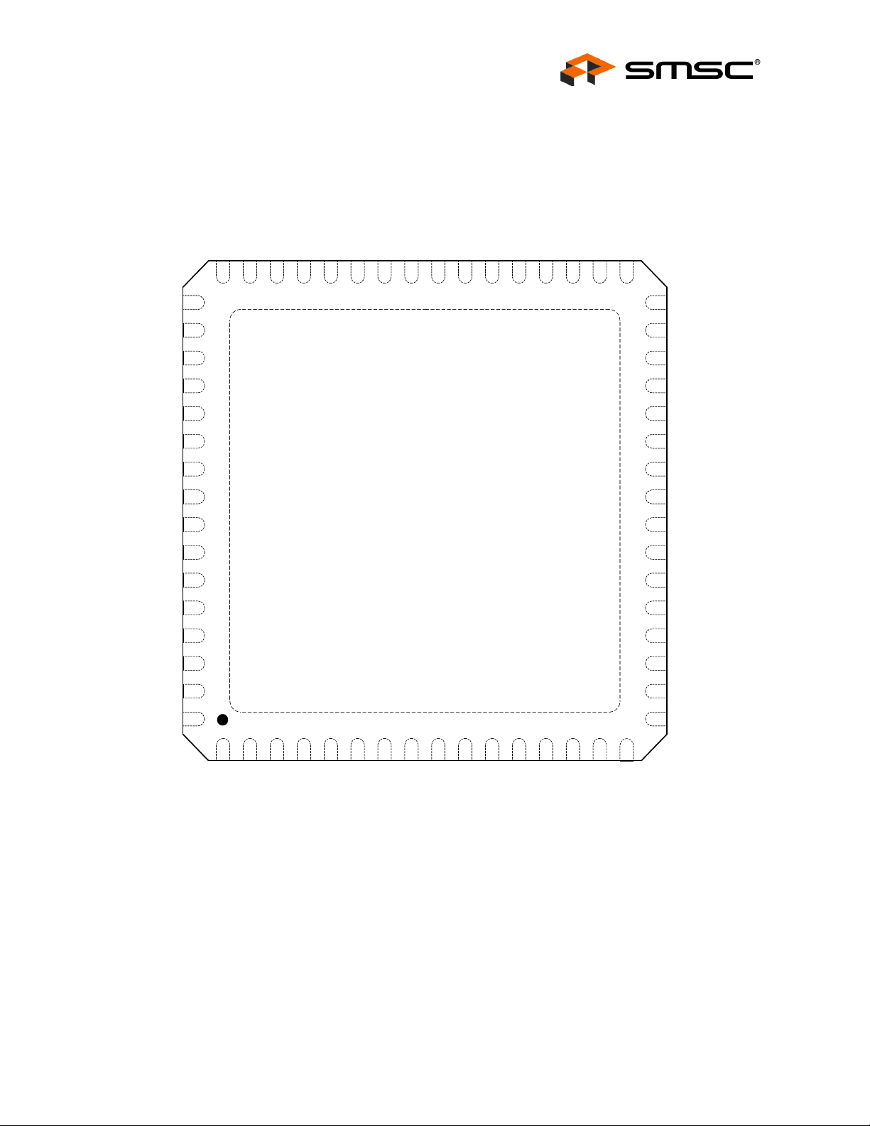
Chapter 2 Pin Description and Configuration
Figure 2.1 LAN9514 64-QFN Pin Assignments (TOP VIEW)
SMSC LAN9514 9 Revision 1.0 (04-20-09)
DATASHEET
Page 10

Table 2.1 EEPROM Pins
USB Hub with Integrated 10/100 Ethernet Controller
Datasheet
NUM
PINS NAME SYMBOL
EEPROM Data
1
1
1
1
NUM
PINS NAME SYMBOL
1
1
In
EEPROM Data
Out
EEPROM Chip
Select
EEPROM Clock EECLK O8 This pin drives the EEPROM clock of the external
JTAG Test Port
Reset
JTAG Test
Mode Select
EEDI IS
EEDO O8 This pin drives the EEDI input of the external
EECS O8 This pin drives the chip select output of the external
nTRST IS This active low pin functions as the JTAG test port
TMS IS This pin functions as the JTAG test mode select.
BUFFER
TYPE DESCRIPTION
This pin is driven by the EEDO output of the
(PD)
Table 2.2 JTAG Pins
BUFFER
TYPE DESCRIPTION
external EEPROM.
EEPROM.
EEPROM.
EEPROM.
reset input.
Note: This pin should be tied high if it is not
used.
JTAG Test Data
1
1
1
NUM
PINS NAME SYMBOL
1
1
Input
JTAG Test Data
Out
JTAG Test
Clock
System Reset nRESET IS This active low pin allows external hardware to
Ethernet
Full-Duplex
Indicator LED
General
Purpose I/O 0
TDI IS This pin functions as the JTAG data input.
TDO O12 This pin functions as the JTAG data output.
TCK IS This pin functions as the JTAG test clock. The
nFDX_LED OD12
GPIO0 IS/O12/
maximum operating frequency of this clock is
25MHz.
Table 2.3 Miscellaneous Pins
BUFFER
TYPE DESCRIPTION
reset the device.
Note: This pin should be tied high if it is not
This pin is driven low (LED on) when the Ethernet
(PU)
OD12
(PU)
link is operating in full-duplex mode.
This General Purpose I/O pin is fully programmable
as either a push-pull output, an open-drain output,
or a Schmitt-triggered input.
used.
Revision 1.0 (04-20-09) 10 SMSC LAN9514
DATASHEET
Page 11

USB Hub with Integrated 10/100 Ethernet Controller
Datasheet
Table 2.3 Miscellaneous Pins (continued)
NUM
PINS NAME SYMBOL
Ethernet Link
Activity Indicator
1
Purpose I/O 1
Ethernet Speed
Indicator LED
1
Purpose I/O 2
1
Purpose I/O 3
LED
General
General
General
nLNKA_LED OD12
GPIO1 IS/O12/
nSPD_LED OD12
GPIO2 IS/O12/
GPIO3 IS/O8/
BUFFER
TYPE DESCRIPTION
This pin is driven low (LED on) when a valid link is
(PU)
OD12
(PU)
(PU)
OD12
(PU)
OD8
(PU)
detected. This pin is pulsed high (LED off) for
80mS whenever transmit or receive activity is
detected. This pin is then driven low again for a
minimum of 80mS, after which time it will repeat
the process if TX or RX activity is detected.
Effectively, LED2 is activated solid for a link. When
transmit or receive activity is sensed, LED2 will
function as an activity indicator.
This General Purpose I/O pin is fully programmable
as either a push-pull output, an open-drain output,
or a Schmitt-triggered input.
This pin is driven low (LED on) when the Ethernet
operating speed is 100Mbs, or during autonegotiation. This pin is driven high during 10Mbs
operation, or during line isolation.
This General Purpose I/O pin is fully programmable
as either a push-pull output, an open-drain output,
or a Schmitt-triggered input.
This General Purpose I/O pin is fully programmable
as either a push-pull output, an open-drain output,
or a Schmitt-triggered input.
1
1
1
1
1
1
General
Purpose I/O 4
General
Purpose I/O 5
General
Purpose I/O 6
General
Purpose I/O 7
Detect
Upstream
VBUS Power
Auto-MDIX
Enable
GPIO4 IS/O8/
OD8
(PU)
GPIO5 IS/O8/
OD8
(PU)
GPIO6 IS/O8/
OD8
(PU)
GPIO7 IS/O8/
OD8
(PU)
VBUS_DET IS_5V This pin detects the state of the upstream bus
AUTOMDIX_EN IS Determines the default Auto-MDIX setting.
This General Purpose I/O pin is fully programmable
as either a push-pull output, an open-drain output,
or a Schmitt-triggered input.
This General Purpose I/O pin is fully programmable
as either a push-pull output, an open-drain output,
or a Schmitt-triggered input.
This General Purpose I/O pin is fully programmable
as either a push-pull output, an open-drain output,
or a Schmitt-triggered input.
This General Purpose I/O pin is fully programmable
as either a push-pull output, an open-drain output,
or a Schmitt-triggered input.
power. The Hub monitors VBUS_DET to determine
when to assert the USBDP0 pin's internal pull-up
resistor (signaling a connect event).
For bus powered hubs, this pin must be tied to
VDD33IO.
For self powered hubs, refer to the LAN9514
reference schematics.
0 = Auto-MDIX is disabled.
1 = Auto-MDIX is enabled.
1
SMSC LAN9514 11 Revision 1.0 (04-20-09)
Test 1 TEST1 - Used for factory testing, this pin must always be left
unconnected.
DATASHEET
Page 12

USB Hub with Integrated 10/100 Ethernet Controller
Table 2.3 Miscellaneous Pins (continued)
Datasheet
NUM
PINS NAME SYMBOL
1
1
1
1
1
NUM
PINS NAME SYMBOL
1
Test 2 TEST2 - Used for factory testing, this pin must always be
Test 3 TEST3 - Used for factory testing, this pin must always be
24 MHz Clock
Enable
24 MHz Clock CLK24_OUT 08 This pin outputs a 24 MHz clock that can be used
Test 4 TEST4 - Used for factory testing, this pin must always be left
Upstream
USB DMINUS 0
CLK24_EN IS This pin enables the generation of the 24 MHz
USBDM0 AIO Upstream USB DMINUS signal.
BUFFER
TYPE DESCRIPTION
connected to VSS for proper operation.
connected to VDD33IO for proper operation.
clock on the CLK_24_OUT pin.
a reference clock for a partner hub.
unconnected.
Table 2.4 USB Pins
BUFFER
TYPE DESCRIPTION
1
1
USB DMINUS 2
1
USB DPLUS 2
1
USB DMINUS 3
1
USB DPLUS 3
1
USB DMINUS 4
1
USB DPLUS 4
1
USB DMINUS 5
1
USB DPLUS 5
Upstream
USB
DPLUS 0
Downstream
Downstream
Downstream
Downstream
Downstream
Downstream
Downstream
Downstream
USBDP0 AIO Upstream USB DPLUS signal.
USBDM2 AIO Downstream USB peripheral 2 DMINUS signal.
USBDP2 AIO Downstream USB peripheral 2 DPLUS signal.
USBDM3 AIO Downstream USB peripheral 3 DMINUS signal.
USBDP3 AIO Downstream USB peripheral 3 DPLUS signal.
USBDM4 AIO Downstream USB peripheral 4 DMINUS signal.
USBDP4 AIO Downstream USB peripheral 4 DPLUS signal.
USBDM5 AIO Downstream USB peripheral 5 DMINUS signal.
USBDP5 AIO Downstream USB peripheral 5 DPLUS signal.
Revision 1.0 (04-20-09) 12 SMSC LAN9514
DATASHEET
Page 13

USB Hub with Integrated 10/100 Ethernet Controller
Datasheet
Table 2.4 USB Pins (continued)
NUM
PINS NAME SYMBOL
USB Port Power
Control 2
1
USB Port Power
Control 3
1
USB Port Power
Control 4
1
PRTCTL2 IS/OD12
PRTCTL3 IS/OD12
PRTCTL4 IS/OD12
BUFFER
TYPE DESCRIPTION
When used as an output, this pin enables power to
(PU)
(PU)
(PU)
downstream USB peripheral 2.
When used as an input, this pin is used to sample
the output signal from an external current monitor
for downstream USB peripheral 2. An overcurrent
condition is indicated when the signal is low.
Refer to Section 2.1 for additional information.
When used as an output, this pin enables power to
downstream USB peripheral 3.
When used as an input, this pin is used to sample
the output signal from an external current monitor
for downstream USB peripheral 3. An overcurrent
condition is indicated when the signal is low.
Refer to Section 2.1 for additional information.
When used as an output, this pin enables power to
downstream USB peripheral 4.
When used as an input, this pin is used to sample
the output signal from an external current monitor
for downstream USB peripheral 4. An overcurrent
condition is indicated when the signal is low.
Refer to Section 2.1 for additional information.
USB Port Power
Control 5
1
1
1
1
1 Crystal Output XO OCLK External 25 MHz crystal output.
External USB
Bias Resistor
USB PLL +1.8V
Power Supply
Crystal Input XI ICLK External 25 MHz crystal input.
PRTCTL5 IS/OD12
(PU)
USBRBIAS AI Used for setting HS transmit current level and on-
VDD18USBPLL P Refer to the LAN9514 reference schematics for
When used as an output, this pin enables power to
downstream USB peripheral 5.
When used as an input, this pin is used to sample
the output signal from an external current monitor
for downstream USB peripheral 5. An overcurrent
condition is indicated when the signal is low.
Refer to Section 2.1 for additional information.
chip termination impedance. Connect to an
external 12K 1.0% resistor to ground.
additional connection information.
Note: This pin can also be driven by a single-
ended clock oscillator. When this method
is used, XO should be left unconnected
SMSC LAN9514 13 Revision 1.0 (04-20-09)
DATASHEET
Page 14

USB Hub with Integrated 10/100 Ethernet Controller
Table 2.5 Ethernet PHY Pins
Datasheet
NUM
PINS NAME SYMBOL
1
1
1
1
Data In Positive
7
1
1
+3.3V Analog
Power Supply
External PHY
Ethernet TX
Data Out
Negative
Ethernet TX
Data Out
Positive
Ethernet RX
Data In
Negative
Ethernet RX
Bias Resistor
Ethernet PLL
+1.8V Power
Supply
TXN AIO Negative output of the Ethernet transmitter. The
TXP AIO Positive output of the Ethernet transmitter. The
RXN AIO Negative input of the Ethernet receiver. The receive
RXP AIO Positive input of the Ethernet receiver. The receive
VDD33A P Refer to the LAN9514 reference schematics for
EXRES AI Used for the internal bias circuits. Connect to an
VDD18ETHPLL P Refer to the LAN9514 reference schematics for
BUFFER
TYPE DESCRIPTION
transmit data outputs may be swapped internally
with receive data inputs when Auto-MDIX is
enabled.
transmit data outputs may be swapped internally
with receive data inputs when Auto-MDIX is
enabled.
data inputs may be swapped internally with
transmit data outputs when Auto-MDIX is enabled.
data inputs may be swapped internally with
transmit data outputs when Auto-MDIX is enabled.
connection information.
external 12.4K 1.0% resistor to ground.
additional connection information.
Table 2.6 I/O Power Pins, Core Power Pins, and Ground Pad
NUM
PINS NAME SYMBOL
5
2
1
Note
2.1
+3.3V I/O
Power
Digital Core
+1.8V Power
Supply Output
Ground VSS P Ground
Note 2.1 Exposed pad on package bottom (Figure 2.1).
VDD33IO P +3.3V Power Supply for I/O Pins.
VDD18CORE P +1.8 V power from the internal core voltage
BUFFER
TYPE DESCRIPTION
Refer to the LAN9514 reference schematics for
connection information.
regulator. All VDD18CORE pins must be tied
together for proper operation.
Refer to the LAN9514 reference schematics for
connection information.
Revision 1.0 (04-20-09) 14 SMSC LAN9514
DATASHEET
Page 15
USB Hub with Integrated 10/100 Ethernet Controller
Datasheet
Table 2.7 64-QFN Package Pin Assignments
PIN
NUM PIN NAME
1 USBDM2 17 PRTCTL4 33 VDD33IO 49 VDD33A
2 USBDP2 18 PRTCTL5 34 TEST2 50 EXRES
3 USBDM3 19 VDD33IO 35 GPIO3 51 VDD33A
4 USBDP3 20 nFDX_LED/
5 VDD33A 21 nLNKA_LED/
6 USBDM4 22 nSPD_LED/
7 USBDP4 23 EECLK 39 VDD33IO 55 TXP
8 USBDM5 24 EECS 40 TEST3 56 TXN
9 USBDP5 25 EEDO 41 AUTOMDIX_EN 57 VDD33A
10 VDD33A 26 EEDI 42 GPIO6 58 USBDM0
11 VBUS_DET 27 VDD33IO 43 GPIO7 59 USBDP0
12 nRESET 28 nTRST 44 CLK24_EN 60 XO
PIN
NUM PIN NAME
GPIO0
GPIO1
GPIO2
PIN
NUM PIN NAME
36 GPIO4 52 RXP
37 GPIO5 53 RXN
38 VDD18CORE 54 VDD33A
PIN
NUM PIN NAME
13 TEST1 29 TMS 45 CLK24_OUT 61 XI
14 PRTCTL2 30 TDI 46 VDD33IO 62 VDD18USBPLL
15 VDD18CORE 31 TDO 47 TEST4 63 USBRBIAS
16 PRTCTL3 32 TCK 48 VDD18ETHPLL 64 VDD33A
MUST BE CONNECTED TO VSS
EXPOSED PAD
SMSC LAN9514 15 Revision 1.0 (04-20-09)
DATASHEET
Page 16

USB Hub with Integrated 10/100 Ethernet Controller
USB Power
Switch
EN
OCS
5V
USB
Device
LAN9514
PRTCTL3
USB Power
Switch
EN
OCS
5V
USB
Device
PRTCTL2
USB Power
Switch
EN
OCS
5V
USB
Device
PRTCTL4
USB Power
Switch
EN
OCS
5V
USB
Device
PRTCTL5
2.1 Port Power Control
This section details the usage of the port power control pins PRTCTL[5:2].
2.1.1 Port Power Control Using a USB Power Switch
The LAN9514 has a single port power control and over-current sense signal for each downstream port.
When disabling port power the driver will actively drive a ‘0’. To avoid unnecessary power dissipation,
the internal pull-up resistor will be disabled at that time. When port power is enabled, the output driver
is disabled and the pull-up resistor is enabled, creating an open drain output. If there is an over-current
situation, the USB Power Switch will assert the open drain OCS signal. The schmitt trigger input will
recognize this situation as a low. The open drain output does not interfere. The overcurrent sense filter
handles the transient conditions, such as low voltage, while the device is powering up.
Datasheet
Figure 2.2 Port Power Control with USB Power Switch
Revision 1.0 (04-20-09) 16 SMSC LAN9514
DATASHEET
Page 17

USB Hub with Integrated 10/100 Ethernet Controller
USB
Device
PRTCTL3
5V
Poly Fuse
LAN9514
USB
Device
PRTCTL2
5V
Poly Fuse
USB
Device
PRTCTL4
5V
Poly Fuse
USB
Device
PRTCTL5
5V
Poly Fuse
Datasheet
2.1.2 Port Power Control Using a Poly Fuse
When using theLAN9514 with a poly fuse, an external diode must be used (See Figure 2.3). When
disabling port power, the driver will drive a ‘0’. This procedure will have no effect since the external
diode will isolate the pin from the load. When port power is enabled, the output driver is disabled and
the pull-up resistor is enabled, which creates an open drain output. This means that the pull-up resistor
is providing 3.3 volts to the anode of the diode. If there is an over-current situation, the poly fuse will
open. This will cause the cathode of the diode to go to 0 volts. The anode of the diode will be at 0.7
volts, and the Schmidt trigger input will register this as a low, resulting in an overcurrent detection. The
open drain output does not interfere.
Figure 2.3 Port Power Control with Poly Fuse
SMSC LAN9514 17 Revision 1.0 (04-20-09)
DATASHEET
Page 18

USB Hub with Integrated 10/100 Ethernet Controller
USB
Device
Poly Fuse
5V
USB
Device
PRTCTL2
LAN9514
PRTCTL3
PRTCTL4
PRTCTL5
Datasheet
Many customers use a single poly fuse to power all their devices. For the ganged situation, all power
control pins must be tied together.
Figure 2.4 Port Power with Ganged Control with Poly Fuse
Revision 1.0 (04-20-09) 18 SMSC LAN9514
DATASHEET
Page 19

USB Hub with Integrated 10/100 Ethernet Controller
Datasheet
2.2 Buffer Types
Table 2.8 Buffer Types
BUFFER TYPE DESCRIPTION
IS Schmitt-triggered Input
IS_5V 5V Tolerant Schmitt-triggered Input
O8 Output with 8mA sink and 8mA source
OD8 Open-drain output with 8mA sink
O12 Output with 12mA sink and 12mA source
OD12 Open-drain output with 12mA sink
PU 50uA (typical) internal pull-up. Unless otherwise noted in the pin description, internal pull-
PD 50uA (typical) internal pull-down. Unless otherwise noted in the pin description, internal
AI Analog input
AIO Analog bi-directional
ICLK Crystal oscillator input pin
OCLK Crystal oscillator output pin
P Power pin
ups are always enabled.
Note: Internal pull-up resistors prevent unconnected inputs from floating. Do not rely on
internal resistors to drive signals external to LAN9514. When connected to a load
that must be pulled high, an external resistor must be added.
pull-downs are always enabled.
Note: Internal pull-down resistors prevent unconnected inputs from floating. Do not rely
on internal resistors to drive signals external to LAN9514. When connected to a
load that must be pulled low, an external resistor must be added.
SMSC LAN9514 19 Revision 1.0 (04-20-09)
DATASHEET
Page 20

USB Hub with Integrated 10/100 Ethernet Controller
Chapter 3 EEPROM Controller (EPC)
LAN9514 may use an external EEPROM to store the default values for the USB descriptors and the
MAC address. The EEPROM controller supports most “93C46” type EEPROMs. A total of nine address
bits are used to support 256/512 byte EEPROMs.
Note: A 3-wire style 2K/4K EEPROM that is organized for 256/512 x 8-bit operation must be used.
The MAC address is used as the default Ethernet MAC address and is loaded into the MAC’s ADDRH
and ADDRL registers. If a properly configured EEPROM is not detected, it is the responsibility of the
Host LAN Driver to set the IEEE addresses.
After a system-level reset occurs, the device will load the default values from a properly configured
EEPROM. The device will not accept USB transactions from the Host until this process is completed.
The EEPROM controller also allows the Host system to read, write and erase the contents of the Serial
EEPROM.
3.1 EEPROM Format
Table 3.1 illustrates the format in which data is stored inside of the EEPROM.
Datasheet
Note the EEPROM offsets are given in units of 16-bit word offsets. A length field with a value of zero
indicates that the field does not exist in the EEPROM. The device will use the field’s HW default value
in this case.
Note: For Device Descriptors, the only valid values for the length are 0 and 18.
Note: For Configuration and Interface Descriptors, the only valid values for the length are 0 and 18.
Note: The EEPROM programmer must ensure that if a String Descriptor does not exist in the
EEPROM, the referencing descriptor must contain 00h for the respective string index field.
Note: If no Configuration Descriptor is present in the EEPROM, then the Configuration Flags affect
the values of bmAttributes and bMaxPower in the Ethernet Controller Configuration Descriptor.
Note: If all String Descriptor lengths are zero, then a Language ID will not be supported.
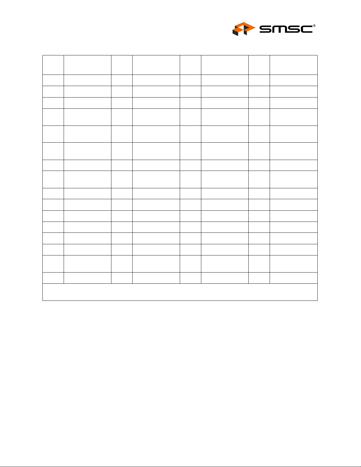
Table 3.1 EEPROM Format
EEPROM ADDRESS EEPROM CONTENTS
00h 0xA5
01h MAC Address [7:0]
02h MAC Address [15:8]
03h MAC Address [23:16]
04h MAC Address [31:24]
05h MAC Address [39:32]
06h MAC Address [47:40]
07h Full-Speed Polling Interval for Interrupt Endpoint
08h Hi-Speed Polling Interval for Interrupt Endpoint
Revision 1.0 (04-20-09) 20 SMSC LAN9514
DATASHEET
Page 21

USB Hub with Integrated 10/100 Ethernet Controller
Datasheet
Table 3.1 EEPROM Format (continued)
09h Configuration Flags
0Ah Language ID Descriptor [7:0]
0Bh Language ID Descriptor [15:8]
0Ch Manufacturer ID String Descriptor Length (bytes)
0Dh Manufacturer ID String Descriptor EEPROM Word Offset
0Eh Product Name String Descriptor Length (bytes)
0Fh Product Name String Descriptor EEPROM Word Offset
10h Serial Number String Descriptor Length (bytes)
11h Serial Number String Descriptor EEPROM Word Offset
12h Configuration String Descriptor Length (bytes)
13h Configuration String Descriptor Word Offset
14h Interface String Descriptor Length (bytes)
15h Interface String Descriptor Word Offset
16h Hi-Speed Device Descriptor Length (bytes)
17h Hi-Speed Device Descriptor Word Offset
18h Hi-Speed Configuration and Interface Descriptor Length (bytes)
19h Hi-Speed Configuration and Interface Descriptor Word Offset
1Ah Full-Speed Device Descriptor Length (bytes)
1Bh Full-Speed Device Descriptor Word Offset
1Ch Full-Speed Configuration and Interface Descriptor Length (bytes)
1Dh Full-Speed Configuration and Interface Descriptor Word Offset
1Eh-1Fh RESERVED
20h Vendor ID LSB Register (VIDL)
21h Vendor ID MSB Register (VIDM)
22h Product ID LSB Register (PIDL)
23h Product ID MSB Register (PIDM)
24h Device ID LSB Register (DIDL)
25h Device ID MSB Register (DIDM)
26h Config Data Byte 1 Register (CFG1)
27h Config Data Byte 2 Register (CFG2)
28h Config Data Byte 3 Register (CFG3)
29h Non-Removable Devices Register (NRD)
2Ah Port Disable (Self) Register (PDS)
2Bh Port Disable (Bus) Register (PDB)
SMSC LAN9514 21 Revision 1.0 (04-20-09)
DATASHEET
Page 22

USB Hub with Integrated 10/100 Ethernet Controller
Table 3.1 EEPROM Format (continued)
2Ch Max Power (Self) Register (MAXPS)
2Dh Max Power (Bus) Register (MAXPB)
2Eh Hub Controller Max Current (Self) Register (HCMCS)
2Fh Hub Controller Max Current (Bus) Register (HCMCB)
30h Power-on Time Register (PWRT)
31h Boost_Up Register (BOOSTUP)
32h Boost_5 Register (BOOST5)
33h Boost_4:2 Register (BOOST42)
34h RESERVED
35h Port Swap Register (PRTSP)
36h Port Remap 12 Register (PRTR12)
37h Port Remap 34 Register (PRTR34)
Datasheet
38h Port Remap 5 Register (PRTR5)
39h Status/Command Register (STCD)
Note: EEPROM byte addresses past 39h can be used to store data for any purpose.
Table 3.2 describes the Configuration Flags
Table 3.2 Configuration Flags Description
BIT NAME DESCRIPTION
7:3 RESERVED 00000b
2 Remote Wakeup Support 0 = The device does not support remote wakeup.
1 RESERVED 0b
0 Power Method 0 = The device Controller is bus powered.
1 = The device supports remote wakeup.
1 = The device Controller is self powered.
Revision 1.0 (04-20-09) 22 SMSC LAN9514
DATASHEET
Page 23

USB Hub with Integrated 10/100 Ethernet Controller
Datasheet
3.1.1 Hub Configuration
EEPROM offsets 20h through 39h comprise the Hub Configuration parameters. Table 3.3 describes
these parameters and their default ROM values (Values assumed if no valid EEPROM present).
Table 3.3 Hub Configuration
EEPROM
OFFSET DESCRIPTION DEFAULT
20h Vendor ID LSB Register (VIDL)
Least Significant Byte of the Vendor ID. This is a 16-bit value that uniquely identifies
the Vendor of the user device (assigned by USB-Interface Forum).
21h Vendor ID MSB (VIDM)
Most Significant Byte of the Vendor ID. This is a 16-bit value that uniquely identifies
the Vendor of the user device (assigned by USB-Interface Forum).
22h Product ID LSB Register (PIDL)
Least Significant Byte of the Product ID. This is a 16-bit value that the Vendor can
assign that uniquely identifies this particular product (assigned by the OEM).
23h Product ID MSB Register (PIDM)
Most Significant Byte of the Product ID. This is a 16-bit value that the Vendor can
assign that uniquely identifies this particular product (assigned by the OEM).
24h Device ID LSB Register (DIDL)
Least Significant Byte of the Device ID. This is a 16-bit device release number in BCD
format (assigned by the OEM).
25h Device ID MSB Register (DIDM)
Most Significant Byte of the Device ID. This is a 16-bit device release number in BCD
format (assigned by the OEM).
26h Config Data Byte 1 Register (CFG1)
Refer to Table 3.4, “Config Data Byte 1 Register (CFG1) Format,” on page 29 for
details.
27h Config Data Byte 2 Register (CFG2)
Refer to Table 3.5, “Config Data Byte 2 Register (CFG2) Format,” on page 30 for
details.
24h
04h
14h
95h
00h
Note 3.1
9Bh
18h
28h Config Data Byte 3 Register (CFG3)
Refer to Table 3.6, “Config Data Byte 3 Register (CFG3) Format,” on page 31 for
details.
29h Non-Removable Devices Register (NRD)
Indicates which port(s) include non-removable devices.
0 = Port is removable
1 = Port is non-removable
Informs the host if one of the active ports has a permanent device that is not
detachable from the Hub.
Note: The device must provide its own descriptor data.
Bit 7 = RESERVED
Bit 6 = RESERVED
Bit 5 = 1; Port 5 non-removable
Bit 4 = 1; Port 4 non-removable
Bit 3 = 1; Port 3 non-removable
Bit 2 = 1; Port 2 non-removable
Bit 1 = 1; Port 1 non-removable
Bit 0 is RESERVED, always = 0b
Note: Bit 1 must be set to 1 by firmware for proper identification of the Ethernet
Controller as a non-removable device.
SMSC LAN9514 23 Revision 1.0 (04-20-09)
00h
02h
DATASHEET
Page 24

USB Hub with Integrated 10/100 Ethernet Controller
Datasheet
Table 3.3 Hub Configuration (continued)
EEPROM
OFFSET DESCRIPTION DEFAULT
2Ah Port Disable (Self) Register (PDS)
Disables 1 or more ports.
0 = Port is available
1 = Port is disabled
During Self-Powered operation, this selects the ports which will be permanently
disabled, and are not available to be enabled or enumerated by a host controller. The
ports can be disabled in any order, the internal logic will automatically report the
correct number of enabled ports to the USB host, and will reorder the active ports in
order to ensure proper function.
Bit 7 = RESERVED
Bit 6 = RESERVED
Bit 5 = 1; Port 5 disabled
Bit 4 = 1; Port 4 disabled
Bit 3 = 1; Port 3 disabled
Bit 2 = 1; Port 2 disabled
Bit 1 = 1; Port 1 disabled
Bit 0 is RESERVED, always = 0b
2Bh Port Disable (Bus) Register (PDB)
Disables 1 or more ports.
0 = Port is available
1 = Port is disabled
During Bus-Powered operation, this selects the ports which will be permanently
disabled, and are not available to be enabled or enumerated by a host controller. The
ports can be disabled in any order, the internal logic will automatically report the
correct number of enabled ports to the USB host, and will reorder the active ports in
order to ensure proper function.
00h
00h
Bit 7 = RESERVED
Bit 6 = RESERVED
Bit 5 = 1; Port 5 disabled
Bit 4 = 1; Port 4 disabled
Bit 3 = 1; Port 3 disabled
Bit 2 = 1; Port 2 disabled
Bit 1 = 1; Port 1 disabled
Bit 0 is RESERVED, always = 0b
2Ch Max Power (Self) Register (MAXPS)
Value in 2mA increments that the Hub consumes from an upstream port (VBUS) when
operating as a self-powered hub. This value includes the hub silicon along with the
combined power consumption (from VBUS) of all associated circuitry on the board.
This value also includes the power consumption of a permanently attached peripheral
if the hub is configured as a compound device, and the embedded peripheral reports
0mA in its descriptors.
Note: The USB2.0 Specification does not permit this value to exceed 100mA.
2Dh Max Power (Bus) Register (MAXPB)
Value in 2mA increments that the Hub consumes from an upstream port (VBUS) when
operating as a bus-powered hub. This value includes the hub silicon along with the
combined power consumption (from VBUS) of all associated circuitry on the board.
This value also includes the power consumption of a permanently attached peripheral
if the hub is configured as a compound device, and the embedded peripheral reports
0mA in its descriptors.
01h
00h
Revision 1.0 (04-20-09) 24 SMSC LAN9514
DATASHEET
Page 25

USB Hub with Integrated 10/100 Ethernet Controller
Datasheet
Table 3.3 Hub Configuration (continued)
EEPROM
OFFSET DESCRIPTION DEFAULT
2Eh Hub Controller Max Current (Self) Register (HCMCS)
Value in 2mA increments that the Hub consumes from an upstream port (VBUS) when
operating as a self-powered hub. This value includes the hub silicon along with the
combined power consumption (from VBUS) of all associated circuitry on the board.
This value does NOT include the power consumption of a permanently attached
peripheral if the hub is configured as a compound device.
Note: The USB2.0 Specification does not permit this value to exceed 100mA.
2Fh Hub Controller Max Current (Bus) Register (HCMCB)
Value in 2mA increments that the Hub consumes from an upstream port (VBUS) when
operating as a bus-powered hub. This value includes the hub silicon along with the
combined power consumption (from VBUS) of all associated circuitry on the board.
This value does NOT include the power consumption of a permanently attached
peripheral if the hub is configured as a compound device.
30h Power-on Time Register (PWRT)
The length of time that it takes (in 2mS intervals) from the time the host initiated
power-on sequence begins on a port until power is good on that port. System software
uses this value to determine how long to wait before accessing a powered-on port.
31h Boost_Up Register (BOOSTUP)
Refer to Table 3.7, “Boost_Up Register (BOOSTUP) Format,” on page 31 for details.
32h Boost_5 Register (BOOST5)
Refer to Table 3.8, “Boost_5 Register (BOOST5) Format,” on page 31 for details.
33h Boost_4:2 Register (BOOST42)
Refer to Table 3.9, “Boost_4:2 Register (BOOST42) Format,” on page 32 for details.
34h RESERVED 00h
01h
00h
32h
00h
00h
00h
35h Port Swap Register (PRTSP)
Swaps the Upstream and Downstream USB DP and DM pins for ease of board routing
to devices and connectors.
0 = USB D+ functionality is associated with the DP pin and D- functionality is
associated with the DM pin.
1 = USB D+ functionality is associated with the DM pin and D- functionality is
associated with the DP pin.
Bit 7 = RESERVED
Bit 6 = RESERVED
Bit 5 = 1; Port 5 DP/DM is swapped
Bit 4 = 1; Port 4 DP/DM is swapped
Bit 3 = 1; Port 3 DP/DM is swapped
Bit 2 = 1; Port 2 DP/DM is swapped
Bit 1 = RESERVED
Bit 0 = 1; Upstream Port DP/DM is swapped
00h
SMSC LAN9514 25 Revision 1.0 (04-20-09)
DATASHEET
Page 26

USB Hub with Integrated 10/100 Ethernet Controller
Bit [7:4] = 0000 Physical Port 2 is Disabled
0001 Physical Port 2 is mapped to Logical Port 1
0010 Physical Port 2 is mapped to Logical Port 2
0011 Physical Port 2 is mapped to Logical Port 3
0100 Physical Port 2 is mapped to Logical Port 4
0101 Physical Port 2 is mapped to Logical Port 5
All others RESERVED
Bit [3:0] = 0000 Physical Port 1 is Disabled
0001 Physical Port 1 is mapped to Logical Port 1
0010 Physical Port 1 is mapped to Logical Port 2
0011 Physical Port 1 is mapped to Logical Port 3
0100 Physical Port 1 is mapped to Logical Port 4
0101 Physical Port 1 is mapped to Logical Port 5
All others RESERVED
Datasheet
Table 3.3 Hub Configuration (continued)
EEPROM
OFFSET DESCRIPTION DEFAULT
36h Port Remap 12 Register (PRTR12)
When a hub is enumerated by a USB Host Controller, the hub is only permitted to
report how many ports it has. The hub is not permitted to select a numerical range or
assignment. The Host Controller will number the downstream ports of the hub starting
with the number 1, up to the number of ports that the hub reported having.
The host’s port number is referred to as “Logical Port Number” and the physical port
on the hub is the “Physical Port Number”. When remapping mode is enabled, (see
Port Re-Mapping Enable (PRTMAP_EN) bit in Config Data Byte 3 Register (CFG3)
Format) the hub’s downstream port numbers can be remapped to different logical port
numbers (assigned by the host).
Note: The OEM must ensure that Contiguous Logical Port Numbers are used,
starting from #1 up to the maximum number of enabled ports. This ensures
that the hub’s ports are numbered in accordance with the way a Host will
communicate with the ports.
21h
Revision 1.0 (04-20-09) 26 SMSC LAN9514
DATASHEET
Page 27

USB Hub with Integrated 10/100 Ethernet Controller
Bit [7:4] = 0000 Physical Port 4 is Disabled
0001 Physical Port 4 is mapped to Logical Port 1
0010 Physical Port 4 is mapped to Logical Port 2
0011 Physical Port 4 is mapped to Logical Port 3
0100 Physical Port 4 is mapped to Logical Port 4
0101 Physical Port 4 is mapped to Logical Port 5
All others RESERVED
Bit [3:0] = 0000 Physical Port 3 is Disabled
0001 Physical Port 3 is mapped to Logical Port 1
0010 Physical Port 3 is mapped to Logical Port 2
0011 Physical Port 3 is mapped to Logical Port 3
0100 Physical Port 3 is mapped to Logical Port 4
0101 Physical Port 3 is mapped to Logical Port 5
All others RESERVED
Datasheet
Table 3.3 Hub Configuration (continued)
EEPROM
OFFSET DESCRIPTION DEFAULT
37h Port Remap 34 Register (PRTR34)
When a hub is enumerated by a USB Host Controller, the hub is only permitted to
report how many ports it has. The hub is not permitted to select a numerical range or
assignment. The Host Controller will number the downstream ports of the hub starting
with the number 1, up to the number of ports that the hub reported having.
The host’s port number is referred to as “Logical Port Number” and the physical port
on the hub is the “Physical Port Number”. When remapping mode is enabled (see
Port Re-Mapping Enable (PRTMAP_EN) bit in Config Data Byte 3 Register (CFG3)
Format), the hub’s downstream port numbers can be remapped to different logical port
numbers (assigned by the host).
Note: The OEM must ensure that Contiguous Logical Port Numbers are used,
starting from #1 up to the maximum number of enabled ports, this ensures
that the hub’s ports are numbered in accordance with the way a Host will
communicate with the ports.
43h
SMSC LAN9514 27 Revision 1.0 (04-20-09)
DATASHEET
Page 28

USB Hub with Integrated 10/100 Ethernet Controller
Bit [7:4] = - RESERVED
Bit [3:0] = 0000 Physical Port 5 is Disabled
0001 Physical Port 5 is mapped to Logical Port 1
0010 Physical Port 5 is mapped to Logical Port 2
0011 Physical Port 5 is mapped to Logical Port 3
0100 Physical Port 5 is mapped to Logical Port 4
0101 Physical Port 5 is mapped to Logical Port 5
All others RESERVED
Datasheet
Table 3.3 Hub Configuration (continued)
EEPROM
OFFSET DESCRIPTION DEFAULT
38h Port Remap 5 Register (PRTR5)
When a hub is enumerated by a USB Host Controller, the hub is only permitted to
report how many ports it has. The hub is not permitted to select a numerical range or
assignment. The Host Controller will number the downstream ports of the hub starting
with the number 1, up to the number of ports that the hub reported having.
The host’s port number is referred to as “Logical Port Number” and the physical port
on the hub is the “Physical Port Number”. When remapping mode is enabled (see
Port Re-Mapping Enable (PRTMAP_EN) bit in Config Data Byte 3 Register (CFG3)
Format) the hub’s downstream port numbers can be remapped to different logical port
numbers (assigned by the host).
Note: The OEM must ensure that Contiguous Logical Port Numbers are used,
starting from #1 up to the maximum number of enabled ports, this ensures
that the hub’s ports are numbered in accordance with the way a Host will
communicate with the ports.
05h
39h Status/Command Register (STCD)
Revision 1.0 (04-20-09) 28 SMSC LAN9514
Refer to Table 3.10, “Status/Command Register (STCD) Format,” on page 32 for
details.
Note 3.1 Default value is dependent on device revision.
01h
DATASHEET
Page 29

USB Hub with Integrated 10/100 Ethernet Controller
Datasheet
Table 3.4 Config Data Byte 1 Register (CFG1) Format
BITS DESCRIPTION DEFAULT
7 Self or Bus Power (SELF_BUS_PWR)
Selects between Self or Bus-Powered operation.
0 = Bus-Powered
1 = Self-Powered
The Hub is either Self-Powered (draws less than 2mA of upstream bus
power) or Bus-Powered (limited to a 100mA maximum of upstream power
prior to being configured by the host controller).
When configured as a Bus-Powered device, the SMSC Hub consumes less
than 100mA of current prior to being configured. After configuration, the BusPowered SMSC Hub (along with all associated hub circuitry, any embedded
devices if part of a compound device, and 100mA per externally available
downstream port) must consume no more than 500mA of upstream VBUS
current. The current consumption is system dependent, and the OEM must
ensure that the USB2.0 specifications are not violated.
When configured as a Self-Powered device, <1mA of upstream VBUS
current is consumed and all ports are available, with each port being capable
of sourcing 500mA of current.
6 RESERVED 0b
5 High Speed Disable (HS_DISABLE)
Disables the capability to attach as either a High/Full-Speed device, and
forces attachment as Full-Speed only (no High-Speed support).
0 = High-/Full-Speed
1 = Full-Speed-Only (High-Speed disabled)
4 Multiple TT Enable (MTT_ENABLE)
Enables one transaction translator per port operation.
1b
0b
1b
Selects between a mode where only one transaction translator is available
for all ports (Single-TT), or each port gets a dedicated transaction translator
(Multi-TT) {Note: The host may force Single-TT mode only}.
0 = Single TT for all ports.
1 = One TT per port (multiple TT's supported)
3 EOP Disable (EOP_DISABLE)
Disables EOP generation of EOF1 when in Full-Speed mode. During FS
operation only, this permits the Hub to send EOP if no downstream traffic is
detected at EOF1. See Section 11.3.1 of the USB 2.0 Specification for
additional details.
Note: Generation of an EOP at the EOF1 point may prevent a Host
controller (operating in FS mode) from placing the USB bus in
suspend.
0 = An EOP is generated at the EOF1 point if no traffic is detected.
1 = EOP generation at EOF1 is disabled (note: this is normal USB
operation).
Note: This is a rarely used feature in the PC environment, existing drivers
may not have been thoroughly debugged with this feature enabled.
It is included because it is a permitted feature in Chapter 11 of the
USB specification.
1b
SMSC LAN9514 29 Revision 1.0 (04-20-09)
DATASHEET
Page 30

USB Hub with Integrated 10/100 Ethernet Controller
Table 3.4 Config Data Byte 1 Register (CFG1) Format (continued)
BITS DESCRIPTION DEFAULT
Datasheet
2:1 Over Current Sense (CURRENT_SNS)
Selects current sensing on a port-by-port basis, all ports ganged, or none
(only for bus-powered hubs) The ability to support current sensing on a port
or ganged basis is hardware implementation dependent.
00 = Ganged sensing (all ports together)
01 = Individual port-by-port
1x = Over current sensing not supported (must only be used with BusPowered configurations!)
0 Port Power Switching (PORT_PWR)
Enables power switching on all ports simultaneously (ganged), or port power
is individually switched on and off on a port by port basis (individual). The
ability to support power enabling on a port or ganged basis is hardware
implementation dependent.
0 = Ganged switching (all ports together)
1 = Individual port by port switching
Table 3.5 Config Data Byte 2 Register (CFG2) Format
BITS DESCRIPTION DEFAULT
7:6 RESERVED 00b
5:4 Over Current Timer (OC_TIMER)
Over Current Timer delay
01b
1b
01b
00 = 50ns
01 = 100ns (This is the recommended value)
10 = 200ns
11 = 400ns
3 Compound Device (COMPOUND)
Allows the OEM to indicate that the Hub is part of a compound (see the USB
Specification for definition) device. The applicable port(s) must also be
defined as having a “Non-Removable Device”.
0 = No
1 = Yes, Hub is part of a compound device
2:0 RESERVED 000b
1b
Revision 1.0 (04-20-09) 30 SMSC LAN9514
DATASHEET
Page 31

USB Hub with Integrated 10/100 Ethernet Controller
Datasheet
Table 3.6 Config Data Byte 3 Register (CFG3) Format
BITS DESCRIPTION DEFAULT
7:4 RESERVED 0h
3 Port Re-Mapping Enable (PRTMAP_EN)
Selects the method used by the Hub to assign port numbers and disable
ports.
0 = Standard Mode. The following EEPROM addresses are used to define
which ports are enabled. The ports mapped as Port’n’ on the Hub are
reported as Port’n’ to the host, unless one of the ports is disabled, then the
higher numbered ports are remapped in order to report contiguous port
numbers to the host.
EEPROM Address 2Ah: Port Disable for Self-Powered operation
EEPROM Address 2Bh: Port Disable for Bus-Powered operation
1 = Port Re-Map mode. The mode enables remapping via the following
EEPROM addresses:
EEPROM Address 36h: Port Remap 12
EEPROM Address 37h: Port Remap 34
EEPROM Address 38h: Port Remap 5
2:0 RESERVED 000b
Table 3.7 Boost_Up Register (BOOSTUP) Format
BITS DESCRIPTION DEFAULT
0b
7:2 RESERVED 000000b
1:0 Upstream USB Electrical Signaling Drive Strength Boost Bit for
Upstream Port A (BOOST_IOUT_A)
00 = Normal electrical drive strength
01 = Elevated electrical drive strength (+4% boost)
10 = Elevated electrical drive strength (+8% boost)
11 = Elevated electrical drive strength (+12% boost)
Table 3.8 Boost_5 Register (BOOST5) Format
BITS DESCRIPTION DEFAULT
7:2 RESERVED 000000b
1:0 Upstream USB Electrical Signaling Drive Strength Boost Bit for
Downstream Port 5 (BOOST_IOUT_5)
00 = Normal electrical drive strength
01 = Elevated electrical drive strength (+4% boost)
10 = Elevated electrical drive strength (+8% boost)
11 = Elevated electrical drive strength (+12% boost)
SMSC LAN9514 31 Revision 1.0 (04-20-09)
00b
00b
DATASHEET
Page 32

USB Hub with Integrated 10/100 Ethernet Controller
Table 3.9 Boost_4:2 Register (BOOST42) Format
BITS DESCRIPTION DEFAULT
Datasheet
7:6 Upstream USB Electrical Signaling Drive Strength Boost Bit for
Downstream Port 4 (BOOST_IOUT_4)
00 = Normal electrical drive strength
01 = Elevated electrical drive strength (+4% boost)
10 = Elevated electrical drive strength (+8% boost)
11 = Elevated electrical drive strength (+12% boost)
5:4 Upstream USB Electrical Signaling Drive Strength Boost Bit for
Downstream Port 3 (BOOST_IOUT_3)
00 = Normal electrical drive strength
01 = Elevated electrical drive strength (+4% boost)
10 = Elevated electrical drive strength (+8% boost)
11 = Elevated electrical drive strength (+12% boost)
3:2 Upstream USB Electrical Signaling Drive Strength Boost Bit for
Downstream Port 2 (BOOST_IOUT_2)
00 = Normal electrical drive strength
01 = Elevated electrical drive strength (+4% boost)
10 = Elevated electrical drive strength (+8% boost)
11 = Elevated electrical drive strength (+12% boost)
1:0 RESERVED 00b
Table 3.10 Status/Command Register (STCD) Format
00b
00b
00b
BITS DESCRIPTION DEFAULT
7:2 RESERVED 000000b
1 Reset (RESET)
Resets the internal memory back to nRESET assertion default settings.
0 = Normal Run/Idle State
1 = Force a reset of the registers to their default state
Note: During this reset, this bit is automatically cleared to its default value
of 0.
0 USB Attach and Write Protect (USB_ATTACH)
0 = Device is in configuration state
1 = Hub will signal a USB attach event to an upstream device, and the
internal memory (address range 00h - FEh) is “write-protected” to prevent
unintentional data corruption.
Note: This bit is write once and is only cleared by assertion of the external
nRESET or POR.
0b
1b
Revision 1.0 (04-20-09) 32 SMSC LAN9514
DATASHEET
Page 33

USB Hub with Integrated 10/100 Ethernet Controller
Datasheet
3.2 EEPROM Defaults
The signature value of 0xA5 is stored at address 0. A different signature value indicates to the
EEPROM controller that no EEPROM or an un-programmed EEPROM is attached to the device. In
this case, the hardware default values are used, as shown in Ta b le 3 .11 .
Table 3.11 EEPROM Defaults
FIELD DEFAULT VALUE
Ethernet Controller
MAC Address
Ethernet Controller
Full-Speed Polling
Interval (mS)
Ethernet Controller
Hi-Speed Polling Interval
(mS)
Ethernet Controller
Configuration Flags
Ethernet Controller
Maximum Power (mA)
Ethernet Controller
Vendor ID
Ethernet Controller
Product ID
3.3 EEPROM Auto-Load
Certain system level resets (USB reset, POR, nRESET, and SRST) cause the EEPROM contents to
be loaded into the device. After a reset, the EEPROM controller attempts to read the first byte of data
from the EEPROM. If the value 0xA5 is read from the first address, then the EEPROM controller will
assume that the external Serial EEPROM is configured for auto-loading. If a value other than 0xA5 is
read from the first address, the EEPROM auto-load will not commense.
FFFFFFFFFFFFh
01h
04h
05h
01h
0424h
EC00h
Note: The EEPROM contents are loaded for both the Hub and the Ethernet Controller as a result of
a POR or nRESET. The USB reset results only in the loading of the MAC address from the
EEPROM. A software reset (SRST) or a EEPROM Reload Command causes the EEPROM
contents related solely to the Ethernet Controller to be loaded.
SMSC LAN9514 33 Revision 1.0 (04-20-09)
DATASHEET
Page 34

USB Hub with Integrated 10/100 Ethernet Controller
3.4 An Example of EEPROM Format Interpretation
Table 3.12 and Table 3.13 provide an example of how the contents of a EEPROM are formatted.
Table 3.12 is a dump of the EEPROM memory (256-byte EEPROM), while Ta bl e 3. 1 3 illustrates, byte
by byte, how the EEPROM is formatted.
Table 3.12 Dump of EEPROM Memory
OFFSET
BYTE VALUE
0000h A5 12 34 56 78 9A BC 01
0008h 04 05 09 04 0A 1D 00 00
0010h 00 00 00 00 00 00 12 22
0018h 12 2B 12 34 12 3D 00 00
0020h 24 04 14 95 00 01 9B 18
0028h 00 02 00 00 01 00 01 00
Datasheet
0030h 32 00 00 00 00 00 21 43
0038h 05 01 0A 03 53 00 4D 00
0040h 53 00 43 00 12 01 00 02
0048h FF 00 01 40 24 04 00 EC
0050h 00 01 01 00 00 01 09 02
0058h 27 00 01 01 00 E0 01 09
0060h 04 00 00 03 FF 00 FF 00
0068h 12 01 00 02 FF 00 FF 40
0070h 24 04 00 EC 00 01 01 00
0078h 00 01 09 02 27 00 01 01
0080h 00 E0 01 09 04 00 00 03
0088h FF 00 FF 00 ....................
0090h - 00FFh ..........................................
Revision 1.0 (04-20-09) 34 SMSC LAN9514
DATASHEET
Page 35

USB Hub with Integrated 10/100 Ethernet Controller
Datasheet
Table 3.13 EEPROM Example - 256 Byte EEPROM
EEPROM
EEPROM
ADDRESS
00h A5 EEPROM Programmed Indicator
01h-06h 12 34 56 78 9A BC MAC Address 12 34 56 78 9A BC
07h 01 Full-Speed Polling Interval for Interrupt Endpoint (1ms)
08h 04 Hi-Speed Polling Interval for Interrupt Endpoint (4ms)
CONTENTS
(HEX) DESCRIPTION
09h 05 Configuration Flags - The device is self powered and supports remote
0Ah-0Bh 09 04 Language ID Descriptor 0409h, English
0Ch 0A Manufacturer ID String Descriptor Length (10 bytes)
0Dh 1D Manufacturer ID String Descriptor EEPROM Word Offset (1Dh)
0Eh 00 Product Name String Descriptor Length (0 bytes - NA)
0Fh 00 Product Name String Descriptor EEPROM Word Offset (Don’t Care)
10h 00 Serial Number String Descriptor Length (0 bytes - NA)
11h 00 Serial Number String Descriptor EEPROM Word Offset (Don’t Care)
12h 00 Configuration String Descriptor Length (0 bytes - NA)
13h 00 Configuration String Descriptor Word Offset (Don’t Care)
14h 00 Interface String Descriptor Length (0 bytes - NA)
15h 00 Interface String Descriptor Word Offset (Don’t Care)
16h 12 Hi-Speed Device Descriptor Length (18 bytes)
17h 22h Hi-Speed Device Descriptor Word Offset (22h)
wakeup.
Corresponds to EEPROM Byte Offset 3Ah
Corresponds to EEPROM Byte Offset 44h
18h 12 Hi-Speed Configuration and Interface Descriptor Length (18 bytes)
19h 2B Hi-Speed Configuration and Interface Descriptor Word Offset (2Bh)
1Ah 12 Full-Speed Device Descriptor Length (18 bytes)
1Bh 34 Full-Speed Device Descriptor Word Offset (34h)
1Ch 12 Full-Speed Configuration and Interface Descriptor Length (18bytes)
1Dh 3D Full-Speed Configuration and Interface Descriptor Word Offset (3Dh)
1Eh 00 RESERVED
1Fh 00 RESERVED
20h 24 Vendor ID LSB Register (VIDL)
21h 04 Vendor ID MSB Register (VIDM)
SMSC LAN9514 35 Revision 1.0 (04-20-09)
Corresponds to EEPROM Byte Offset 56h
Corresponds to EEPROM Byte Offset 68h
Corresponds to EEPROM Byte Offset 7Ah
DATASHEET
Page 36

USB Hub with Integrated 10/100 Ethernet Controller
Table 3.13 EEPROM Example - 256 Byte EEPROM (continued)
EEPROM
EEPROM
ADDRESS
22h 14 Product ID LSB Register (PIDL)
23h 95 Product ID MSB Register (PIDM)
24h 00 Device ID LSB Register (DIDL)
25h 01 Device ID MSB Register (DIDM)
26h 9B Config Data Byte 1 Register (CFG1)
27h 18 Config Data Byte 2 Register (CFG2)
28h 00 Config Data Byte 3 Register (CFG3)
29h 02 Non-Removable Devices Register (NRD)
2Ah 00 Port Disable (Self) Register (PDS)
2Bh 00 Port Disable (Bus) Register (PDB)
CONTENTS
(HEX) DESCRIPTION
Datasheet
2Ch 01 Max Power (Self) Register (MAXPS)
2Dh 00 Max Power (Bus) Register (MAXPB)
2Eh 01 Hub Controller Max Current (Self) Register (HCMCS)
2Fh 00 Hub Controller Max Current (Bus) Register (HCMCB)
30h 32 Power-on Time Register (PWRT)
31h 00 Boost_Up Register (BOOSTUP)
32h 00 Boost_7:5 Register (BOOST75)
33h 00 Boost_4:2 Register (BOOST42)
34h 00 RESERVED
35h 00 Port Swap Register (PRTSP)
36h 21 Port Remap 12 Register (PRTR12)
37h 43 Port Remap 34 Register (PRTR34)
38h 05 Port Remap 5 Register (PRTR5)
39h 01 Status/Command Register (STCD)
3A 0A Size of Manufacturer ID String Descriptor (10 bytes)
3Bh 03 Descriptor Type (String Descriptor - 03h)
3Ch-43h 53 00 4D 00 53 00 43 00 Manufacturer ID String (“SMSC” in UNICODE)
44h 12 Size of Hi-Speed Device Descriptor in Bytes (18 bytes)
45h 01 Descriptor Type (Device Descriptor - 01h)
46h-47h 00 02 USB Specification Number that the device complies with (0200h)
48h FF Class Code
Revision 1.0 (04-20-09) 36 SMSC LAN9514
DATASHEET
Page 37

USB Hub with Integrated 10/100 Ethernet Controller
Datasheet
Table 3.13 EEPROM Example - 256 Byte EEPROM (continued)
EEPROM
ADDRESS
49h 00 Subclass Code
4Ah FF Protocol Code
4Bh 40 Maximum Packet Size for Endpoint 0
4Ch-4Dh 24 04 Vendor ID (0424h)
4Eh-4Fh 00 EC Product ID (EC00h)
50h-51h 00 01 Device Release Number (0100h)
52h 01 Index of Manufacturer String Descriptor
53h 00 Index of Product String Descriptor
54h 00 Index of Serial Number String Descriptor
55h 01 Number of Possible Configurations
56h 09 Size of Hi-Speed Configuration Descriptor in bytes (9 bytes)
57h 02 Descriptor Type (Configuration Descriptor - 02h)
58h-59h 27 00 Total length in bytes of data returned (0027h = 39 bytes)
5Ah 01 Number of Interfaces
EEPROM
CONTENTS
(HEX) DESCRIPTION
5Bh 01 Value to use as an argument to select this configuration
5Ch 00 Index of String Descriptor describing this configuration
5Dh E0 Self powered and remote wakeup enabled
5Eh 01 Maximum Power Consumption is 2 mA
5Fh 09 Size of Descriptor in Bytes (9 Bytes)
60h 04 Descriptor Type (Interface Descriptor - 04h)
61h 00 Number identifying this Interface
62h 00 Value used to select alternative setting
63h 03 Number of Endpoints used for this interface (Less endpoint 0)
64h FF Class Code
65h 00 Subclass Code
66h FF Protocol Code
67h 00 Index of String Descriptor Describing this interface
68h 12 Size of Full-Speed Device Descriptor in Bytes (18 Bytes)
69h 01 Descriptor Type (Device Descriptor - 01h)
6Ah-6Bh 00 02 USB Specification Number that the device complies with (0200h)
6Ch FF Class Code
SMSC LAN9514 37 Revision 1.0 (04-20-09)
DATASHEET
Page 38

USB Hub with Integrated 10/100 Ethernet Controller
Table 3.13 EEPROM Example - 256 Byte EEPROM (continued)
EEPROM
EEPROM
ADDRESS
6Dh 00 Subclass Code
6Eh FF Protocol Code
6Fh 40 Maximum Packet Size for Endpoint 0
70h-71h 24 04 Vendor ID (0424h)
72h-73h 00 EC Product ID (EC00h)
74h-75h 00 01 Device Release Number (0100h)
76 01 Index of Manufacturer String Descriptor
77h 00 Index of Product String Descriptor
78h 00 Index of Serial Number String Descriptor
79h 01 Number of Possible Configurations
CONTENTS
(HEX) DESCRIPTION
Datasheet
7Ah 09 Size of Full-Speed Configuration Descriptor in bytes (9 bytes)
7Bh 02 Descriptor Type (Configuration Descriptor - 02h)
7Ch-7Dh 27 00 Total length in bytes of data returned (0027h = 39 bytes)
7Eh 01 Number of Interfaces
7Fh 01 Value to use as an argument to select this configuration
80h 00 Index of String Descriptor describing this configuration
81h E0 Self powered and remote wakeup enabled
82h 01 Maximum Power Consumption is 2 mA
83h 09 Size of Full-Speed Interface Descriptor in Bytes (9 Bytes)
84h 04 Descriptor Type (Interface Descriptor - 04h)
85h 00 Number identifying this Interface
86h 00 Value used to select alternative setting
87h 03 Number of Endpoints used for this interface (Less endpoint 0)
88h FF Class Code
89h 00 Subclass Code
8Ah FF Protocol Code
8Bh 00 Index of String Descriptor describing this interface
8Ch-FFh - Data storage for use by Host as desired
Revision 1.0 (04-20-09) 38 SMSC LAN9514
DATASHEET
Page 39

USB Hub with Integrated 10/100 Ethernet Controller
Datasheet
Chapter 4 Operational Characteristics
4.1 Absolute Maximum Ratings*
Supply Voltage (VDD33IO, VDD33A) (Note 4.1). . . . . . . . . . . . . . . . . . . . . . . . . . . . . . . . . .0V to +3.6V
Positive voltage on signal pins, with respect to ground (Note 4.2) . . . . . . . . . . . . . . . . . . . . . . . . . . +6V
Negative voltage on signal pins, with respect to ground (Note 4.3) . . . . . . . . . . . . . . . . . . . . . . . . -0.5V
Positive voltage on XI, with respect to ground . . . . . . . . . . . . . . . . . . . . . . . . . . . . . . . . . . . . . . . .+4.6V
Positive voltage on XO, with respect to ground . . . . . . . . . . . . . . . . . . . . . . . . . . . . . . . . . . . . . . .+2.5V
Ambient Operating Temperature in Still Air (T
Storage Temperature . . . . . . . . . . . . . . . . . . . . . . . . . . . . . . . . . . . . . . . . . . . . . . . . . . .-55
Lead Temperature Range. . . . . . . . . . . . . . . . . . . . . . . . . . . . . . . . . .Refer to JEDEC Spec. J-STD-020
HBM ESD Performance per JESD 22-A114-E . . . . . . . . . . . . . . . . . . . . . . . . . . . . . . . . . . . . . . .+/- 8kV
Contact Discharge ESD Performance per IEC61000-4-2 (Note 4.4) . . . . . . . . . . . . . . . . . . . . . .+/- 8kV
Air-Gap Discharge ESD Performance per IEC61000-4-2 (Note 4.4) . . . . . . . . . . . . . . . . . . . . .+/- 15kV
Latch-up Performance per EIA/JESD 78 . . . . . . . . . . . . . . . . . . . . . . . . . . . . . . . . . . . . . . . . .+/- 200mA
Note 4.1 When powering this device from laboratory or system power supplies, it is important that
the absolute maximum ratings not be exceeded or device failure can result. Some power
supplies exhibit voltage spikes on their outputs when AC power is switched on or off. In
addition, voltage transients on the AC power line may appear on the DC output. If this
possibility exists, it is suggested that a clamp circuit be used.
Note 4.2 This rating does not apply to the following pins: XI, XO, EXRES, USBRBIAS.
Note 4.3 This rating does not apply to the following pins: EXRES, USBRBIAS.
Note 4.4 Performed by independant 3rd party test facility.
) . . . . . . . . . . . . . . . . . . . . . . . . . . . . . . . . 0oC to +70oC
A
o
C to +150oC
*Stresses exceeding those listed in this section could cause permanent damage to the device. This is
a stress rating only. Exposure to absolute maximum rating conditions for extended periods may affect
device reliability. Functional operation of the device at any condition exceeding those indicated in
Section 4.2, "Operating Conditions**", Section 4.4, "DC Specifications", or any other applicable section
of this specification is not implied. Note, device signals are NOT 5 volt tolerant unless specified
otherwise.
4.2 Operating Conditions**
Supply Voltage (VDD33A, VDD33BIAS, VDD33IO) . . . . . . . . . . . . . . . . . . . . . . . . . . .+3.3V +/- 300mV
Ambient Operating Temperature in Still Air (T
**Proper operation of LAN9514 is guaranteed only within the ranges specified in this section.
SMSC LAN9514 39 Revision 1.0 (04-20-09)
DATASHEET
) . . . . . . . . . . . . . . . . . . . . . . . . . . . . . . . . 0oC to +70oC
A
Page 40

USB Hub with Integrated 10/100 Ethernet Controller
4.3 Power Consumption
This section details the power consumption of the device as measured during various modes of
operation. Power dissipation is determined by temperature, supply voltage, and external source/sink
requirements.
4.3.1 Operational Current Consumption & Power Dissipation
Table 4.1 Operational Current Consumption & Power Dissipation (VDD33IO = VDD33A = 3.3V)
PARAMETER MIN TYPICAL MAX UNIT
100BASE-TX Full Duplex (USB High-Speed)
Supply current (VDD33IO, VDD33A) 288 mA
Power Dissipation (Device Only) 951 mW
10BASE-T Full Duplex (USB High-Speed)
Supply current (VDD33IO, VDD33A) 243 mA
Power Dissipation (Device Only) 802 mW
Datasheet
10BASE-T Full Duplex (USB Full-Speed)
Supply current (VDD33IO, VDD33A) 180 mA
Power Dissipation (Device Only) 594 mW
Note: All values measured with maximum simultaneous traffic on the Ethernet port and all USB ports.
Note: Magnetic power consumption:
100BASE-TX: ~42mA
10BASE-T: ~104mA
Revision 1.0 (04-20-09) 40 SMSC LAN9514
DATASHEET
Page 41

USB Hub with Integrated 10/100 Ethernet Controller
Datasheet
4.4 DC Specifications
Table 4.2 I/O Buffer Characteristics
PARAMETER SYMBOL MIN TYP MAX UNITS NOTES
IS Type Input Buffer
Low Input Level
High Input Level
Negative-Going Threshold
Positive-Going Threshold
SchmittTrigger Hysteresis
- V
(V
IHT
ILT
)
Input Leakage
(VIN = VSS or VDD33IO)
Input Capacitance
IS_5V Type Input Buffer
Low Input Level
High Input Level
Negative-Going Threshold
Positive-Going Threshold
SchmittTrigger Hysteresis
- V
(V
IHT
ILT
)
Input Leakage
(VIN = VSS or VDD33IO)
Input Leakage
(VIN = 5.5V)
V
V
V
V
V
V
V
C
V
V
V
ILI
IHI
ILT
IHT
HYS
I
IH
IN
ILI
IHI
ILT
IHT
HYS
I
IH
I
IH
-0.3
1.01
1.39
345
-10
-0.3
1.01
1.39
345
-10
1.18
1.6
420
1.18
1.6
420
3.6
1.35
1.8
485
10
2.5
5.5
1.35
1.8
485
10
120
V
V
V
V
mV
uA
pF
V
V
V
V
mV
uA
uA
Schmitt trigger
Schmitt trigger
Note 4.5
Schmitt trigger
Schmitt trigger
Note 4.5
Note 4.5, Note 4.6
Input Capacitance
C
IN
3.5
pF
O8 Type Buffers
Low Output Level
High Output Level
V
OL
V
OH
VDD33IO - 0.4
0.4 V
V
IOL = 8mA
IOH = -8mA
OD8 Type Buffer
Low Output Level V
OL
0.4 V IOL = 8mA
O12 Type Buffers
Low Output Level
High Output Level
V
OL
V
OH
VDD33IO - 0.4
0.4 V
V
IOL = 12mA
IOH = -12mA
OD12 Type Buffer
Low Output Level V
ICLK Type Buffer (XI Input)
Low Input Level
High Input Level
OL
V
ILI
V
IHI
-0.3
1.4
0.4 V IOL = 12mA
Note 4.7
0.5
3.6
V
V
Note 4.5 This specification applies to all inputs and tri-stated bi-directional pins. Internal pull-down
and pull-up resistors add +/- 50uA per-pin (typical)
SMSC LAN9514 41 Revision 1.0 (04-20-09)
DATASHEET
Page 42

USB Hub with Integrated 10/100 Ethernet Controller
Datasheet
Note 4.6 This is the total 5.5V input leakage for the entire device.
Note 4.7 XI can optionally be driven from a 25MHz single-ended clock oscillator.
Table 4.3 100BASE-TX Transceiver Characteristics
PARAMETER SYMBOL MIN TYP MAX UNITS NOTES
Peak Differential Output Voltage High V
Peak Differential Output Voltage Low V
Signal Amplitude Symmetry V
Signal Rise and Fall Time T
Rise and Fall Symmetry T
Duty Cycle Distortion D
Overshoot and Undershoot V
PPH
PPL
SS
RF
RFS
CD
OS
950 - 1050 mVpk Note 4.8
-950 - -1050 mVpk Note 4.8
98 - 102 % Note 4.8
3.0 - 5.0 nS Note 4.8
--0.5nSNote 4.8
35 50 65 % Note 4.9
--5%
Jitter 1.4 nS Note 4.10
Note 4.8 Measured at line side of transformer, line replaced by 100Ω (+/- 1%) resistor.
Note 4.9 Offset from 16nS pulse width at 50% of pulse peak.
Note 4.10 Measured differentially.
Table 4.4 10BASE-T Transceiver Characteristics
PARAMETER SYMBOL MIN TYP MAX UNITS NOTES
Transmitter Peak Differential Output Voltage V
Receiver Differential Squelch Threshold V
OUT
DS
2.2 2.5 2.8 V Note 4.11
300 420 585 mV
Note 4.11 Min/max voltages guaranteed as measured with 100Ω resistive load.
Revision 1.0 (04-20-09) 42 SMSC LAN9514
DATASHEET
Page 43

USB Hub with Integrated 10/100 Ethernet Controller
25 pF
OUTPUT
Datasheet
4.5 AC Specifications
This section details the various AC timing specifications of the LAN9514.
Note: The USBDP and USBDM pin timing adheres to the USB 2.0 specification. Refer to the
Universal Serial Bus Revision 2.0 specification for detailed USB timing information.
4.5.1 Equivalent Test Load
Output timing specifications assume the 25pF equivalent test load illustrated in Figure 4.1 below.
4.5.2 Reset Timing
The nRESET pin input assertion time must be a minimum of 1 μS. Assertion of nRESET is not a
requirement. However, if used, it must be asserted for the minimum period specified.
Figure 4.1 Output Equivalent Test Load
SMSC LAN9514 43 Revision 1.0 (04-20-09)
DATASHEET
Page 44

4.5.3 EEPROM Timing
EECLK
EEDO
EEDI
EECS
t
ckldis
t
cshckh
EEDI (VERIFY)
t
ckhtckl
t
ckcyc
t
cklcsl
t
csl
t
dvckhtckhdis
t
dsckh
t
dhckh
t
dhcsl
t
cshdv
The following specifies the EEPROM timing requirements for LAN9514:
USB Hub with Integrated 10/100 Ethernet Controller
Datasheet
Figure 4.1 EEPROM Timing
Table 4.5 EEPROM Timing Values
SYMBOL DESCRIPTION MIN TYP MAX UNITS
t
ckcyc
t
ckh
t
ckl
t
cshckh
t
cklcsl
t
dvckh
t
ckhdis
t
dsckh
t
dhckh
t
ckldis
t
cshdv
t
dhcsl
t
csl
EECLK Cycle time 1110 1130 ns
EECLK High time 550 570 ns
EECLK Low time 550 570 ns
EECS high before rising edge of EECLK 1070 ns
EECLK falling edge to EECS low 30 ns
EEDO valid before rising edge of EECLK 550 ns
EEDO disable after rising edge EECLK 550 ns
EEDI setup to rising edge of EECLK 90 ns
EEDI hold after rising edge of EECLK 0 ns
EECLK low to data disable (OUTPUT) 580 ns
EEDIO valid after EECS high (VERIFY) 600 ns
EEDIO hold after EECS low (VERIFY) 0 ns
EECS low 1070 ns
Revision 1.0 (04-20-09) 44 SMSC LAN9514
DATASHEET
Page 45

USB Hub with Integrated 10/100 Ethernet Controller
Datasheet
4.6 Clock Circuit
LAN9514 can accept either a 25MHz crystal (preferred) or a 25MHz single-ended clock oscillator (+/50ppm) input. If the single-ended clock oscillator method is implemented, XO should be left
unconnected and XI should be driven with a nominal 0-3.3V clock signal. The input clock duty cycle
is 40% minimum, 50% typical and 60% maximum.
It is recommended that a crystal utilizing matching parallel load capacitors be used for the crystal
input/output signals (XI/XO). See Table 4.6 for the recommended crystal specifications.
Table 4.6 LAN9514 Crystal Specifications
PARAMETER SYMBOL MIN NOM MAX UNITS NOTES
Crystal Cut AT, typ
Crystal Oscillation Mode Fundamental Mode
Crystal Calibration Mode Parallel Resonant Mode
Frequency F
Frequency Tolerance @ 25
o
CF
Frequency Stability Over Temp F
Frequency Deviation Over Time F
fund
tol
temp
age
Total Allowable PPM Budget - - +/-50 PPM Note 4.14
Shunt Capacitance C
Load Capacitance C
Drive Level P
Equivalent Series Resistance R
O
L
W
1
Operating Temperature Range 0 - +70
- 25.000 - MHz
- - +/-50 PPM Note 4.12
- - +/-50 PPM Note 4.12
- +/-3 to 5 - PPM Note 4.13
-7 typ-pF
- 20 typ - pF
300 - - uW
--50Ohm
o
C
LAN9514 XI Pin Capacitance - 3 typ - pF Note 4.15
LAN9514 XO Pin Capacitance - 3 typ - pF Note 4.15
Note 4.12 The maximum allowable values for Frequency Tolerance and Frequency Stability are
application dependant. Since any particular application must meet the IEEE +/-50 PPM
Total PPM Budget, the combination of these two values must be approximately +/-45 PPM
(allowing for aging).
Note 4.13 Frequency Deviation Over Time is also referred to as Aging.
Note 4.14 The total deviation for the Transmitter Clock Frequency is specified by IEEE 802.3u as
+/- 50 PPM.
Note 4.15 This number includes the pad, the bond wire and the lead frame. PCB capacitance is not
included in this value. The XO/XI pin and PCB capacitance values are required to
accurately calculate the value of the two external load capacitors. These two external load
capacitors determine the accuracy of the 25.000 MHz frequency.
SMSC LAN9514 45 Revision 1.0 (04-20-09)
DATASHEET
Page 46

Chapter 5 Package Outline
5.1 64-QFN Package
USB Hub with Integrated 10/100 Ethernet Controller
Datasheet
Figure 5.1 LAN9514 64-QFN Package Definition
Table 5.1 LAN9514 64-QFN Dimensions
MIN NOMINAL MAX REMARKS
A 0.80 0.85 1.00 Overall Package Height
A1 0.00 0.02 0.05 Standoff
A2 - 0.65 0.80 Mold Cap Thickness
D/E 8.90 9.00 9.10 X/Y Body Size
D1/E1 8.65 8.75 8.85 X/Y Mold Cap Size
D2/E2 7.20 7.30 7.40 X/Y Exposed Pad Size
L 0.30 0.40 0.50 Terminal Length
b 0.18 0.25 0.30 Terminal Width
e 0.50 BSC Terminal Pitch
K 0.35 - - Pin to Center Pad Clearance
Revision 1.0 (04-20-09) 46 SMSC LAN9514
DATASHEET
Page 47

USB Hub with Integrated 10/100 Ethernet Controller
Datasheet
Notes:
1. All dimensions are in millimeters unless otherwise noted.
2. Dimension “b” applies to plated terminals and is measured between 0.15 and 0.30 mm from the terminal tip.
3. Details of terminal #1 identifier are optional, but must be located within the area indicated. The terminal #1
identifier may be either a mold or marked feature.
Figure 5.2 LAN9514 Recommended PCB Land Pattern
SMSC LAN9514 47 Revision 1.0 (04-20-09)
DATASHEET
 Loading...