

Page 1

LAN9500/LAN9500i
Hi-Speed USB 2.0 to 10/100
Ethernet Controller
PRODUCT FEATURES
Highlights
Sin gle Chip Hi-Speed USB 2.0 to 10/100 Ethernet
Controller
Integra ted 10/100 Ethernet MAC with Full-Duplex
Support
Integra ted 10/100 Ethernet PHY with HP Auto-MDIX
support
Integra ted USB 2.0 Hi-Speed Device Controller
Integra ted USB 2.0 Hi-Speed PHY
Impleme nts Reduced Power Operating Modes
Target Applications
Embed ded Systems
Set-Top Boxes
PVR’s
CE Devices
Ne tworked Printers
USB Po rt Replicators
Standalone USB to Ethernet Dongles
Test Instrumentation
Industrial
Key Benefits
USB De vice Controller
— Fully compliant with Hi-Speed Universal Serial Bus
Specification Revision 2.0
— Supports HS (480 Mbps) and FS (12 Mbps) modes
— Four endpoints supported
— Supports vendor specific commands
— Integrated USB 2.0 PHY
— Remote wakeup supported
Hi gh-Performance 10/100 Ethernet Controller
— Fully compliant with IEEE802.3/802.3u
— Integrated Ethernet MAC and PHY
— 10BASE-T and 100BASE-TX support
— Full- and half-duplex support
— Full- and half-duplex flow control
Datasheet
— Preamble generation and removal
— Automatic 32-bit CRC generation and checking
— Automatic payload padding and pad removal
— Loop-back modes
— TCP/UDP/IP/ICMP checksum offload support
— Flexible address filtering modes
– One 48-bit perfect address
– 64 hash-filtered multicast addresses
– Pass all multicast
– Promiscuous mode
– Inverse filtering
– Pass all incoming with status report
— Wakeup packet support
— Integrated Ethernet PHY
– Auto-negotiation
– Automatic polarity detection and correction
– HP Auto-MDIX support
– Link status change wake-up detection
— Support for 3 status LEDs
— External MII and Turbo MII support HomePNA™ and
HomePlug® PHY
Po wer and I/Os
— Various low power modes
—11 GPIOs
— Supports bus-powered and self-powered operation
— Integrated power-on reset circuit
— External 3.3v I/O supply
– Internal 1.8v core supply regulator
Misce llaneous Features
— EEPROM Controller
— IEEE 1149.1 (JTAG) Boundary Scan
— Requires single 25 MHz crystal
Software
— Windows XP/Vista Driver
— Linux Driver
— Win CE Driver
—MAC OS Driver
— EEPROM Utility
Packaging
— 56-pin QFN (8x8 mm) Lead-Free RoHS Compliant
package
Environmental
— Commercial Temperature Range (0°C to +70°C)
— Industrial Temperature Range (-40°C to +85°C)
SMSC LAN9500/LAN9500i Revision 1.7 (10-02-08)
DATASHEET
Page 2

Hi-Speed USB 2.0 to 10/100 Ethernet Controller
Datasheet
ORDER NUMBER(S):
LAN9500-ABZJ FOR 56-PIN, QFN LEAD-FREE ROHS COMPLIANT PACKAGE (0 TO +70°C TEMP RANGE)
LAN9500i-ABZJ FOR 56-PIN, QFN LEAD-FREE ROHS COMPLIANT PACKAGE (-40 TO +85°C TEMP RANGE)
80 ARKAY DRIVE, HAUPPAUGE, NY 11788 (631) 435-6000, FAX (631) 273-3123
Copyright © 2008 SMSC or its subsidiaries. All rights reserved.
Circuit diagrams and other information relating to SMSC products are included as a mean s of illustrating typical applications. Conse quently, complete information sufficient for
construction purposes is not necessarily given. Although the information has been checked and is believed to be accurate, no responsibility is assumed for inaccuracies. SMSC
reserves the right to make changes to specifications and product descriptions at any time without notice. Contact your local SMSC sales office to obtain the latest specifications
before placing your product order. The provision of this information does not convey to the purchaser of the described semiconductor devices any licenses under any patent
rights or other intellectual property rights of SMSC or others. All sales are expressly conditional on your agreement to the terms and conditions of the most recently da ted
version of SMSC's standard Terms of Sale Agreement dated before the date of your order (the "Terms of Sale Agreement"). The product may contain design defects or errors
known as anomalies which may cause the product's functions to deviate from published specifications. Anomaly sheets are available upon request. SMSC products are not
designed, intended, authorized or warranted for use in any life support or other application where product failure could cause or contribute to personal injury or severe property
damage. Any and all such uses without prior written approval of an Officer of SMSC and further testing and/or modification will be fully at the risk of the customer. Copies of
this document or other SMSC literature, as well as the Terms of Sale Agreement, may be obtained by visiting SMSC’s website at http://www.smsc.com. SMSC is a registered
trademark of Standard Microsystems Corporation (“SMSC”). Product names and company names are the trademarks of their respective holders.
SMSC DISCLAIMS AND EXCLUDES ANY AND ALL WARRANTIES, INCLUDING WITHOUT LIMITATION ANY AND ALL IMPLIED WARRANTIES OF MERCHANTABILITY,
FITNESS FOR A PARTICULAR PURPOSE, TITLE, AND AGAINST INFRINGEMENT AND THE LIKE, AND ANY AND ALL WARRANTIES ARISING FROM ANY COURSE
OF DEALING OR USAGE OF TRADE. IN NO EVENT SHALL SMSC BE LIABLE FOR ANY DIRECT, INCIDENTAL, INDIRECT, SPECIAL, PUNITIVE, OR CONSEQUENTIAL
DAMAGES; OR FOR LOST DATA, PROFITS, SAVINGS OR REVENUES OF ANY KIND; REGARDLESS OF THE FORM OF ACTION, WHETHER BASED ON CONTRACT;
TORT; NEGLIGENCE OF SMSC OR OTHERS; STRICT LIABILITY; BREACH OF WARRANTY; OR OTHERWISE; WHETHER OR NOT ANY REMEDY OF BUYER IS HELD
TO HAVE FAILED OF ITS ESSENTIAL PURPOSE, AND WHETHER OR NOT SMSC HAS BEEN ADVISED OF THE POSSIBILITY OF SUCH DAMAGES.
SMSC LAN9500/LAN9500i 2 Revision 1.7 (10-02-08)
DATASHEET
Page 3

Hi-Speed USB 2.0 to 10/100 Ethernet Controller
Datasheet
Table of Contents
Chapter 1 Introduction . . . . . . . . . . . . . . . . . . . . . . . . . . . . . . . . . . . . . . . . . . . . . . . . . . . . . . . 6
1.1 Block Diagram . . . . . . . . . . . . . . . . . . . . . . . . . . . . . . . . . . . . . . . . . . . . . . . . . . . . . . . . . . . . . . . . . 6
1.1.1 Overview . . . . . . . . . . . . . . . . . . . . . . . . . . . . . . . . . . . . . . . . . . . . . . . . . . . . . . . . . . . . . . 6
1.1.2 USB . . . . . . . . . . . . . . . . . . . . . . . . . . . . . . . . . . . . . . . . . . . . . . . . . . . . . . . . . . . . . . . . . . 7
1.1.3 FIFO Controller . . . . . . . . . . . . . . . . . . . . . . . . . . . . . . . . . . . . . . . . . . . . . . . . . . . . . . . . . 7
1.1.4 Ethernet. . . . . . . . . . . . . . . . . . . . . . . . . . . . . . . . . . . . . . . . . . . . . . . . . . . . . . . . . . . . . . . 7
1.1.5 Power Management . . . . . . . . . . . . . . . . . . . . . . . . . . . . . . . . . . . . . . . . . . . . . . . . . . . . . 7
1.1.6 EEPROM Controller . . . . . . . . . . . . . . . . . . . . . . . . . . . . . . . . . . . . . . . . . . . . . . . . . . . . . 8
1.1.7 General Purpose I/O . . . . . . . . . . . . . . . . . . . . . . . . . . . . . . . . . . . . . . . . . . . . . . . . . . . . . 8
Chapter 2 Pin Description and Configuration . . . . . . . . . . . . . . . . . . . . . . . . . . . . . . . . . . . . 9
2.1 Buffer Types . . . . . . . . . . . . . . . . . . . . . . . . . . . . . . . . . . . . . . . . . . . . . . . . . . . . . . . . . . . . . . . . . . 19
Chapter 3 EEPROM Controller (EPC). . . . . . . . . . . . . . . . . . . . . . . . . . . . . . . . . . . . . . . . . 20
3.1 EEPROM Format . . . . . . . . . . . . . . . . . . . . . . . . . . . . . . . . . . . . . . . . . . . . . . . . . . . . . . . . . . . . . . 20
3.2 EEPROM Defaults . . . . . . . . . . . . . . . . . . . . . . . . . . . . . . . . . . . . . . . . . . . . . . . . . . . . . . . . . . . . . 22
3.3 EEPROM Auto-Load. . . . . . . . . . . . . . . . . . . . . . . . . . . . . . . . . . . . . . . . . . . . . . . . . . . . . . . . . . . . 22
3.4 An Example of EEPROM Format Interpretation . . . . . . . . . . . . . . . . . . . . . . . . . . . . . . . . . . . . . . . 23
Chapter 4 Operational Characteristics . . . . . . . . . . . . . . . . . . . . . . . . . . . . . . . . . . . . . . . . . 28
4.1 Absolute Maximum Ratings*. . . . . . . . . . . . . . . . . . . . . . . . . . . . . . . . . . . . . . . . . . . . . . . . . . . . . . 28
4.2 Operating Conditions**. . . . . . . . . . . . . . . . . . . . . . . . . . . . . . . . . . . . . . . . . . . . . . . . . . . . . . . . . . 28
4.3 Power Consumption . . . . . . . . . . . . . . . . . . . . . . . . . . . . . . . . . . . . . . . . . . . . . . . . . . . . . . . . . . . . 29
4.3.1 SUSPEND0 . . . . . . . . . . . . . . . . . . . . . . . . . . . . . . . . . . . . . . . . . . . . . . . . . . . . . . . . . . . 29
4.3.2 SUSPEND1 . . . . . . . . . . . . . . . . . . . . . . . . . . . . . . . . . . . . . . . . . . . . . . . . . . . . . . . . . . . 29
4.3.3 SUSPEND2 . . . . . . . . . . . . . . . . . . . . . . . . . . . . . . . . . . . . . . . . . . . . . . . . . . . . . . . . . . . 29
4.3.4 Operational Power Consumption. . . . . . . . . . . . . . . . . . . . . . . . . . . . . . . . . . . . . . . . . . . 30
4.3.5 Customer Evaluation Board Operational Power Consumption . . . . . . . . . . . . . . . . . . . . 30
4.4 DC Specifications . . . . . . . . . . . . . . . . . . . . . . . . . . . . . . . . . . . . . . . . . . . . . . . . . . . . . . . . . . . . . . 31
4.5 AC Specifications . . . . . . . . . . . . . . . . . . . . . . . . . . . . . . . . . . . . . . . . . . . . . . . . . . . . . . . . . . . . . . 33
4.5.1 Equivalent Test Load. . . . . . . . . . . . . . . . . . . . . . . . . . . . . . . . . . . . . . . . . . . . . . . . . . . . 33
4.5.2 Power-On Configuration Strap Valid Timing . . . . . . . . . . . . . . . . . . . . . . . . . . . . . . . . . . 34
4.5.3 Reset and Configuration Strap Timing . . . . . . . . . . . . . . . . . . . . . . . . . . . . . . . . . . . . . . 35
4.5.4 EEPROM Timing . . . . . . . . . . . . . . . . . . . . . . . . . . . . . . . . . . . . . . . . . . . . . . . . . . . . . . . 36
4.5.5 Turbo MII Interface Timing . . . . . . . . . . . . . . . . . . . . . . . . . . . . . . . . . . . . . . . . . . . . . . . 37
4.6 Clock Circuit . . . . . . . . . . . . . . . . . . . . . . . . . . . . . . . . . . . . . . . . . . . . . . . . . . . . . . . . . . . . . . . . . . 39
Chapter 5 Package Outline . . . . . . . . . . . . . . . . . . . . . . . . . . . . . . . . . . . . . . . . . . . . . . . . . . . 40
Chapter 6 Revision History. . . . . . . . . . . . . . . . . . . . . . . . . . . . . . . . . . . . . . . . . . . . . . . . . . . 42
SMSC LAN9500/LAN9500i 3 Revision 1.7 (10-02-08)
DATASHEET
Page 4

Hi-Speed USB 2.0 to 10/100 Ethernet Controller
Datasheet
List of Figures
Figure 1.1 LAN9500/LAN9500i System Diagram . . . . . . . . . . . . . . . . . . . . . . . . . . . . . . . . . . . . . . . . . . . 6
Figure 2.1 LAN9500/LAN9500i 56-QFN Pin Assignments (TOP VIEW). . . . . . . . . . . . . . . . . . . . . . . . . . 9
Figure 4.1 Output Equivalent Test Load . . . . . . . . . . . . . . . . . . . . . . . . . . . . . . . . . . . . . . . . . . . . . . . . . 33
Figure 4.2 Power-On Configuration Strap Valid Timing . . . . . . . . . . . . . . . . . . . . . . . . . . . . . . . . . . . . . 34
Figure 4.3 nRESET Reset Pin Timing. . . . . . . . . . . . . . . . . . . . . . . . . . . . . . . . . . . . . . . . . . . . . . . . . . . 35
Figure 4.4 EEPROM Timing . . . . . . . . . . . . . . . . . . . . . . . . . . . . . . . . . . . . . . . . . . . . . . . . . . . . . . . . . . 36
Figure 4.1 Turbo MII Output Timing . . . . . . . . . . . . . . . . . . . . . . . . . . . . . . . . . . . . . . . . . . . . . . . . . . . . 37
Figure 4.2 Turbo MII Input Timing. . . . . . . . . . . . . . . . . . . . . . . . . . . . . . . . . . . . . . . . . . . . . . . . . . . . . . 37
Figure 5.1 LAN9500/LAN9500i 56-QFN Package. . . . . . . . . . . . . . . . . . . . . . . . . . . . . . . . . . . . . . . . . . 40
Figure 5.2 LAN9500/LAN9500i 56-QFN Recommended PCB Land Pattern . . . . . . . . . . . . . . . . . . . . . 41
Revision 1.7 (10-02-08) 4 SMSC LAN9500/LAN9500i
DATASHEET
Page 5

Hi-Speed USB 2.0 to 10/100 Ethernet Controller
Datasheet
List Of Tables
Table 2.1 MII Interface Pins. . . . . . . . . . . . . . . . . . . . . . . . . . . . . . . . . . . . . . . . . . . . . . . . . . . . . . . . . . . 10
Table 2.2 EEPROM Pins. . . . . . . . . . . . . . . . . . . . . . . . . . . . . . . . . . . . . . . . . . . . . . . . . . . . . . . . . . . . . 13
Table 2.3 JTAG Pins . . . . . . . . . . . . . . . . . . . . . . . . . . . . . . . . . . . . . . . . . . . . . . . . . . . . . . . . . . . . . . . . 13
Table 2.4 Miscellaneous Pins . . . . . . . . . . . . . . . . . . . . . . . . . . . . . . . . . . . . . . . . . . . . . . . . . . . . . . . . . 14
Table 2.5 USB Pins . . . . . . . . . . . . . . . . . . . . . . . . . . . . . . . . . . . . . . . . . . . . . . . . . . . . . . . . . . . . . . . . . 16
Table 2.6 Ethernet PHY Pins. . . . . . . . . . . . . . . . . . . . . . . . . . . . . . . . . . . . . . . . . . . . . . . . . . . . . . . . . . 16
Table 2.7 I/O Power Pins, Core Power Pins, and Ground Pad . . . . . . . . . . . . . . . . . . . . . . . . . . . . . . . . 17
Table 2.8 No-Connect Pins . . . . . . . . . . . . . . . . . . . . . . . . . . . . . . . . . . . . . . . . . . . . . . . . . . . . . . . . . . . 17
Table 2.9 56-QFN Package Pin Assignments . . . . . . . . . . . . . . . . . . . . . . . . . . . . . . . . . . . . . . . . . . . . . 18
Table 2.10 Buffer Types . . . . . . . . . . . . . . . . . . . . . . . . . . . . . . . . . . . . . . . . . . . . . . . . . . . . . . . . . . . . . . 19
Table 3.1 EEPROM Format. . . . . . . . . . . . . . . . . . . . . . . . . . . . . . . . . . . . . . . . . . . . . . . . . . . . . . . . . . . 20
Table 3.2 Configuration Flags Description. . . . . . . . . . . . . . . . . . . . . . . . . . . . . . . . . . . . . . . . . . . . . . . . 21
Table 3.3 EEPROM Defaults. . . . . . . . . . . . . . . . . . . . . . . . . . . . . . . . . . . . . . . . . . . . . . . . . . . . . . . . . . 22
Table 3.4 Dump of EEPROM Memory. . . . . . . . . . . . . . . . . . . . . . . . . . . . . . . . . . . . . . . . . . . . . . . . . . . 23
Table 3.5 EEPROM Example - 256 Byte EEPROM . . . . . . . . . . . . . . . . . . . . . . . . . . . . . . . . . . . . . . . . 24
Table 4.1 SUSPEND0 - Supply and Current @3.3V. . . . . . . . . . . . . . . . . . . . . . . . . . . . . . . . . . . . . . . . 29
Table 4.2 SUSPEND1 - Supply and Current @3.3V. . . . . . . . . . . . . . . . . . . . . . . . . . . . . . . . . . . . . . . . 29
Table 4.3 SUSPEND2 - Supply and Current @3.3V. . . . . . . . . . . . . . . . . . . . . . . . . . . . . . . . . . . . . . . . 29
Table 4.4 Operational Power Consumption - Supp ly and Current @3.3V. . . . . . . . . . . . . . . . . . . . . . . . 30
Table 4.5 Customer Evaluation Board Operational Power Consumption - Supply and Current @3.3V . 30
Table 4.6 I/O Buffer Characteristics. . . . . . . . . . . . . . . . . . . . . . . . . . . . . . . . . . . . . . . . . . . . . . . . . . . . . 31
Table 4.7 100BASE-TX Transceiver Characteristics. . . . . . . . . . . . . . . . . . . . . . . . . . . . . . . . . . . . . . . . 32
Table 4.8 10BASE-T Transceiver Characteristics. . . . . . . . . . . . . . . . . . . . . . . . . . . . . . . . . . . . . . . . . . 32
Table 4.9 Power-On Configuration Strap Valid Timing . . . . . . . . . . . . . . . . . . . . . . . . . . . . . . . . . . . . . . 34
Table 4.10 n RESET Reset Pin Timing Values . . . . . . . . . . . . . . . . . . . . . . . . . . . . . . . . . . . . . . . . . . . . . 35
Table 4.11 EEPROM Timing Values . . . . . . . . . . . . . . . . . . . . . . . . . . . . . . . . . . . . . . . . . . . . . . . . . . . . . 36
Table 4.12 Turbo MII Output Timing Values . . . . . . . . . . . . . . . . . . . . . . . . . . . . . . . . . . . . . . . . . . . . . . . 37
Table 4.13 Turbo MII Interface Timing Values. . . . . . . . . . . . . . . . . . . . . . . . . . . . . . . . . . . . . . . . . . . . . . 38
Table 4.14 LAN9500/LAN9500i Crystal Specifications . . . . . . . . . . . . . . . . . . . . . . . . . . . . . . . . . . . . . . . 39
Table 5.1 LAN9500/LAN9500i 56-QFN Dimensions . . . . . . . . . . . . . . . . . . . . . . . . . . . . . . . . . . . . . . . . 40
Table 6.1 Customer Revision History . . . . . . . . . . . . . . . . . . . . . . . . . . . . . . . . . . . . . . . . . . . . . . . . . . . 42
Table 6.2 Datasheet Revision History (INTERNAL) . . . . . . . . . . . . . . . . . . . . . . . . . . . . . . . . . . . . . . . . 43
SMSC LAN9500/LAN9500i 5 Revision 1.7 (10-02-08)
DATASHEET
Page 6
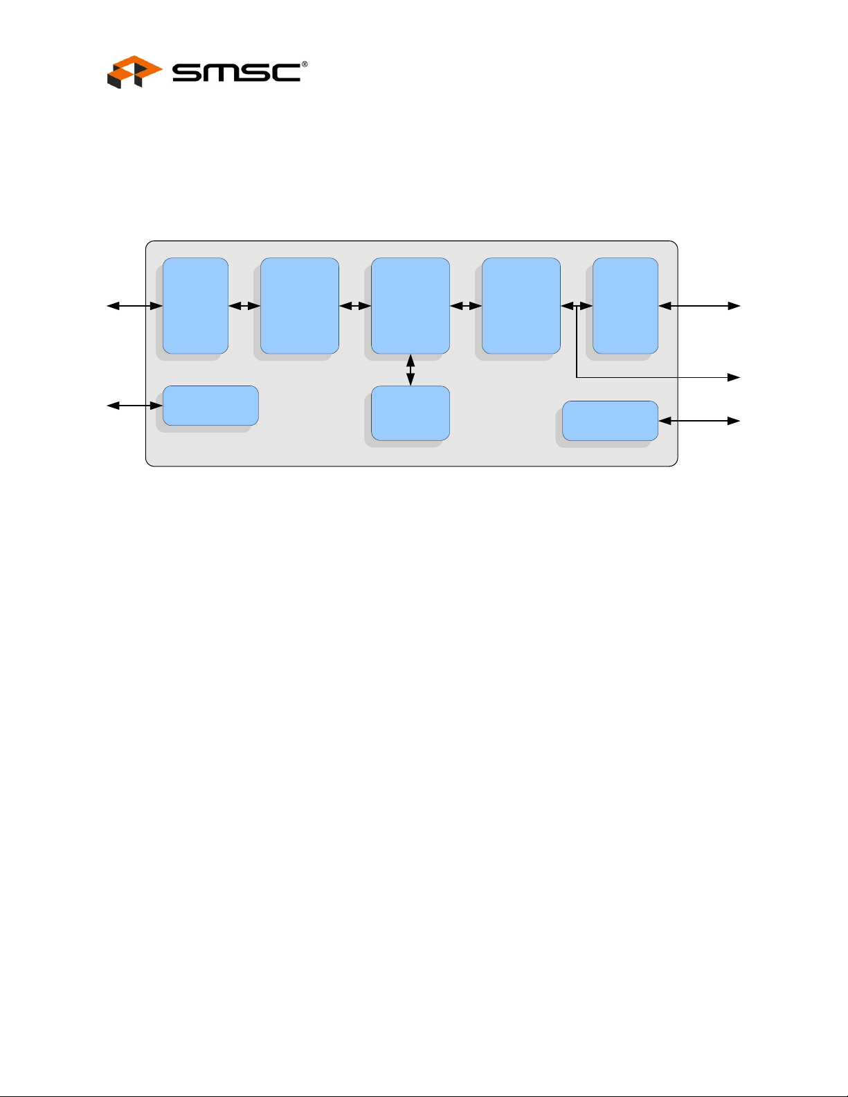
Chapter 1 Introduction
1.1 Block Diagram
Hi-Speed USB 2.0 to 10/100 Ethernet Controller
Datasheet
USB
USB
PHY
JTAG
TAP
Controller
LAN9500/LAN9500i
1.1.1 Overview
The LAN9500/LAN9500i is a high performance Hi-Speed USB 2.0 to 10/100 Ethernet controller. With
applications ranging from embedded systems, set-top boxes, and PVR’s, to USB port replicators, USB
to Ethernet dongles, and test instrumentation, the LAN9500/LAN9500i is a high performance and co st
competitive USB to Ethernet connectivity solution.
The LAN9500/LAN9500i contains an integrated 10/100 Ethernet PHY, USB PHY, Hi-Speed USB 2.0
device controller, 10/100 Ethernet MAC, TAP controller, EEPROM controller, and a FIFO controller with
a total of 30 KB of internal packet buffering.
USB 2.0
Device
Controller
FIFO
Controller
10/100
Ethernet
MAC
SRAM
Figure 1.1 LAN9500/LAN9500i Sy stem Diagram
Ethernet
PHY
EEPROM
Controller
Ethernet
MII: To optional
external PHY
EEPROM
The internal USB 2.0 device controller and USB PHY are compliant with the USB 2.0 Hi-Speed
standard. The LAN9500/LAN9500i implements Control, Interrupt, Bulk-in, and Bulk-out USB Endpoints.
The Ethernet controller supports auto-negotiation, auto-polarity correction, HP Auto-MDIX, and is
compliant with the IEEE 802.3 and IEEE 802.3u standards. An external MII interface provides support
for an external Fast Ethernet PHY, HomePNA, and HomePlug functionality.
Multiple power management features are provided, including various low power modes and "Magic
Packet", "Wake On LAN", and "Link Status Change" wake events. These wake events can be
programmed to initiate a USB remote wakeup.
An internal EEPROM controller exists to load various USB configuration information and the device
MAC address. The integrated IEEE 1149.1 compliant TAP controller provides boundary scan via JTAG.
Revision 1.7 (10-02-08) 6 SMSC LAN9500/LAN9500i
DATASHEET
Page 7

Hi-Speed USB 2.0 to 10/100 Ethernet Controller
Datasheet
1.1.2 USB
The USB portion of the LAN9500/LAN9500i integrates a Hi-Speed USB 2.0 device controller and USB
PHY.
The USB device controller contains a USB low-level protocol interpreter which implements the USB
bus protocol, packet generation/extraction, PID/Device ID parsing, and CRC coding/decoding, with
autonomous error handling. The USB device controller is capable of operating in USB 2.0 Hi-Speed
and Full-Speed compliant modes and contains autonomous protocol handling functions such as
handling of suspend/resume/reset conditions, remote wakeup, and stall condition clearing on Setup
packets. The USB device controller also autonomously handles error conditions such as retry for CRC
and data toggle errors, and generates NYET, STALL, ACK and NACK handshake responses,
depending on the endpoint buffer status.
The LAN9500/LAN9500i implements four USB endpoints: Control, Interrupt, Bulk-in, and Bulk-out. The
Bulk-in and Bulk-out Endpoints allow for Ethernet reception and transmission respectively.
Implementation of vendor-specific commands allows for efficient statistics gathering and access to the
LAN9500/LAN9500i system control and status registers.
1.1.3 FIFO Controller
The FIFO controller uses an internal SRAM to buffer RX and TX traffic. Bulk-out packets from the USB
controller are directly stored into the TX buffer. Ethernet Frames are directly stored into the RX buffer
and become the basis for bulk-in packets.
1.1.4 Ethernet
The LAN9500/LAN9500i integrates an IEEE 802.3 PHY for twisted pair Ethernet applications and a
10/100 Ethernet Media Access Controller (MAC).
The PHY can be configured for either 100 Mbps (100BASE-TX) or 10 Mbps (10BASE-T) Ethernet
operation in either full- or half-duplex configurations and includes auto-negotiation, auto-polarity
correction, and Auto-MDIX. Minimal external components are required for the utilization of the
Integrated PHY.
Optionally, an external PHY may be used via the MII (Media Independent Interface) port, effectively
bypassing the internal PHY. This option allo ws support for HomePNA and HomePlug applications.
The Ethernet MAC/PHY supports numerous power management wakeup features, including “Magic
Packet”, “Wake on LAN”, and “Link Status Change”.
1.1.5 Power Management
The LAN9500/LAN9500i features three variations of USB suspend: SUSPEND0, SUSPEND1, and
SUSPEND2. These modes allow the application to select the ideal balance of remote wakeup
functionality and power consumption.
SUSPEND0: Supports GPIO, “Wake On LAN”, and “Magic Packet” remote wakeup events. This
suspend state reduces power by stopping the clocks of the MAC and other internal modules.
SUSPEND1: Supports GPIO and “Link Status Change” for remote wakeup events. This suspend
state consumes less power than SUSPEND0.
SUSPEND2: Supports only GPIO assertion for a remote wake up event. This suspend state
consumes less than 1 mA. This is the default suspend mode for the LAN9500/L AN9500i.
SMSC LAN9500/LAN9500i 7 Revision 1.7 (10-02-08)
DATASHEET
Page 8

1.1.6 EEPROM Controller
The LAN9500/LAN9500i contains an EEPROM controller for connection to an external EEPROM. This
allows for the automatic loading of static configuration data upon power-on reset, pin reset, or software
reset. The EEPROM can be configured to load USB descriptors, USB device configuration, and MAC
address.
1.1.7 General Purpose I/O
When configured for internal PHY mode, up to ele ven GPIOs are supported. All GPIOs can serve as
remote wakeup events when the LAN9500/LAN9500i is in a suspended state.
Hi-Speed USB 2.0 to 10/100 Ethernet Controller
Datasheet
Revision 1.7 (10-02-08) 8 SMSC LAN9500/LAN9500i
DATASHEET
Page 9
Hi-Speed USB 2.0 to 10/100 Ethernet Controller
Datasheet
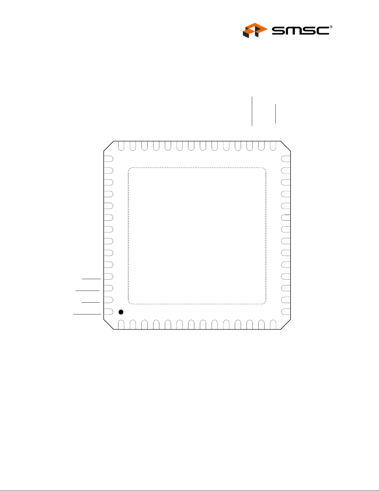
Chapter 2 Pin Description and Configuration
RXCLK
TDI/RXD3
TMS/RXD2
TCK/RXD1
TDO/nPHY_RST
nTRST/RXD0
VDD33IO
PHY_SEL
TEST3
EEDI
EEDO/AUTOMDIX_EN
EECS
RXDV
42
41
40
39
38
37
36
35
34
33
32
31
EECLK/PWR_SEL
30
29
TXEN
RXER
CRS/GPIO3
COL/GPIO0
TXCLK
VDD33IO
TEST1
VDD18CORE
VDD33IO
VDD33IO
TXD3/GPIO7/EEP_SIZE
TXD2/GPIO6/PORT_SWAP
TXD1/GPIO5/RMT_WKP
TXD0/GPIO4/EEP_DISABLE
43
44
45
46
47
48
49
50
51
52
53
54
55
56
1
2
TXN
nPHY_INT
LAN9500/LAN9500i
3
4
TXP
VDD33A
SMSC
56 PIN QFN
(TOP VIEW)
VSS
5
6
7
RXP
RXN
VDD33A
8
9
10
11
12
13
EXRES
VDD33A
USBDM
VDD18PLL
TEST2
USBDP
28
27
26
25
24
23
22
21
20
19
18
17
16
15
14
NC
nSPD_LED/GPIO10
nLNKA_LED/GPIO9
nFDX_LED/GPIO8
VDD33IO
nRESET
MDIO/GPIO1
MDC/GPIO2
VDD18CORE
VBUS_DET
XO
XI
VDD18USBPLL
USBRBIAS
VDD33A
NOTE: When HP Auto-MDIX is activated, the TXN/TXP pins can function as RXN/RXP and vice-versa
NOTE: Exposed pad (VSS) on bottom of package must be connected to gr ound
Figure 2.1 LAN9500/LAN9500i 56-QF N Pin Assignments (TOP VIEW)
SMSC LAN9500/LAN9500i 9 Revision 1.7 (10-02-08)
DATASHEET
Page 10

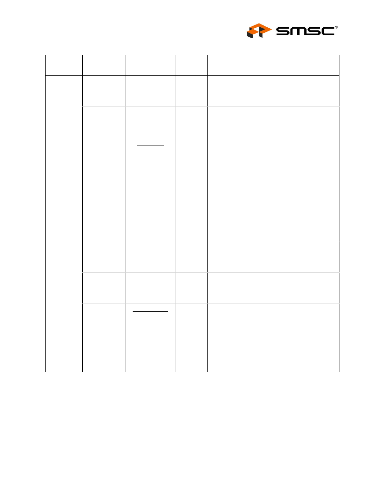
NUM PINS NAME SYMBOL
Hi-Speed USB 2.0 to 10/100 Ethernet Controller
Datasheet
Ta b le 2.1 MII Interface Pins
BUFFER
TYPE DESCRIPTION
Receive Error
1
1
1
1
1
1
(External
PHY Mode)
Transmit
Enable
(External
PHY Mode)
Receive Data
Valid
(External
PHY Mode)
Receive
Clock
(External
PHY Mode)
Carrier Sense
(External
PHY Mode)
General
Purpose I/O 3
(Internal PHY
Mode Only)
MII Collision
Detect
(External
PHY Mode)
General
Purpose I/O 0
(Internal PHY
Mode Only)
RXER IS
(PD)
TXEN O8
(PD)
RXDV IS
(PD)
RXCLK IS
(PD)
CRS IS
(PD)
GPIO3 IS/O8/
OD8
(PU)
COL IS
(PD)
GPIO0 IS/O8/
OD8
(PU)
Receive Error: In external PHY mode, the signal
on this pin is input from the external PHY and
indicates a receive error in the packet. In internal
PHY mode, this pin is not used.
Transmit Enable: In external PHY mode, this pin
output to the external PHY and indicates valid
data on TXD[3:0]. In internal PHY mode, this pin
is not used.
Receive Data Valid: In external PHY mode, the
signal on this pin is input from the external PHY
and indicates valid data on RXD[3:0]. In internal
PHY mode, this pin is not used.
Receive Clock: In external PHY mode, this pin
is the receiver clock input from the external PHY.
In internal PHY mode, this pin is not used.
Carrier Sense: In external PHY mode, the signal
on this pin is input from the external PHY and
indicates a network carrier.
General Purpose I/O 3
MII Collision Detect: In external PHY mode, the
signal on this pin is input from the external PHY
and indicates a collision event.
General Purpose I/O 0
Management
Data
(External
PHY Mode)
1
General
Purpose I/O 1
(Internal PHY
Mode Only)
Management
Clock
(External
PHY Mode)
1
General
Purpose I/O 2
(Internal PHY
Mode Only)
Revision 1.7 (10-02-08) 10 SMSC LAN9500/LAN9500i
MDIO IS/O8
(PD)
GPIO1 IS/O8/
OD8
(PU)
MDC O8
(PD)
GPIO2 IS/O8/
OD8
(PU)
Management Data: In external PHY mode, this
pin provides the management data to/from the
external PHY.
General Purpose I/O 1
Management Clock: In external PHY mode, this
pin outputs the management clock to the external
PHY.
General Purpose I/O 2
DATASHEET
Page 11
Hi-Speed USB 2.0 to 10/100 Ethernet Controller
Datasheet
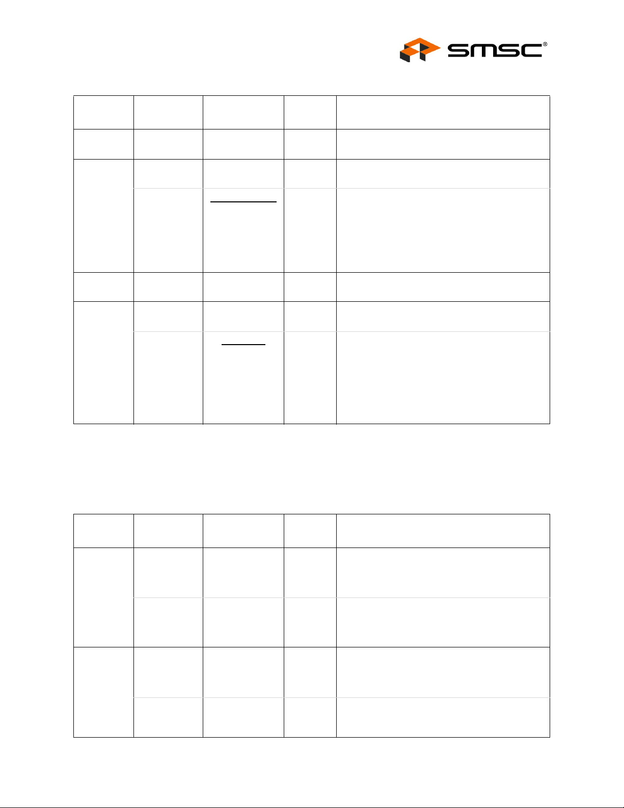
T able 2.1 MII Interface Pins (continued)
NUM PINS NAME SYMBOL
BUFFER
TYPE DESCRIPTION
Transmit Data
3
(External
PHY Mode)
General
Purpose I/O 7
(Internal PHY
Mode Only)
EEPROM
Size
1
Configuration
Strap
Transmit Data
2
(External
PHY Mode)
TXD3 O8
(PU)
GPIO7 IS/O8/
OD8
(PU)
EEP_SIZE IS
(PU)
TXD2 O8
(PD)
Transmit Data 3: In external PHY mode, this pin
functions as the transmit data 3 output to the
external PHY.
General Purpose I/O 7
EEPROM SIZE: The EEP_SIZE strap selects the
size of the EEPROM attached to the
LAN9500/LAN9500i.
0 = 128 byte EEPROM is attached and a total of
seven address bits are used.
1 = 256/512 byte EEPROM is attached and a
total of nine address bits are used.
Note: A 3-wire style 1K/2K/4K EEPROM that
is organized for 128 x 8-bit or 256/512 x
8-bit operation must be used.
See Note 2.1 for more information on
configuration straps.
Transmit Data 2: In external PHY mode, this pin
functions as the transmit data 2 output to the
external PHY.
General
Purpose I/O 6
(Internal PHY
Mode Only)
1
USB Port
Swap
Configuration
Strap
GPIO6 IS/O8/
PORT_SWAP
OD8
(PU)
IS
(PD)
General Purpose I/O 6
USB Port Swap Configuration Strap: Swaps
the mapping of USBDP and USBDM.
0 = USBDP maps to the USB D+ line and
USBDM maps to the USB D- line.
1 = USBDP maps to the USB D- line. USBDM
maps to the USB D+ line.
See Note 2.1 for more information on
configuration straps.
SMSC LAN9500/LAN9500i 11 Revision 1.7 (10-02-08)
DATASHEET
Page 12

T able 2.1 MII Interface Pins (continued)
NUM PINS NAME SYMBOL
Hi-Speed USB 2.0 to 10/100 Ethernet Controller
Datasheet
BUFFER
TYPE DESCRIPTION
Transmit Data
1
(External
PHY Mode)
General
Purpose I/O 5
(Internal PHY
1
1
Mode Only)
Remote
Wakeup
Configuration
Strap
Transmit Data
0
(External
PHY Mode)
General
Purpose I/O 4
(Internal PHY
Mode Only)
EEPROM
Disable
Configuration
Strap
TXD1 O8
(PD)
GPIO5 IS/O8/
OD8
(PU)
RMT_WKP
TXD0 O8
GPIO4 IS/O8/
EEP_DISABLE IS
IS
(PD)
(PD)
OD8
(PU)
(PD)
Transmit Data 1: In external PHY mode, this pin
functions as the transmit data 1 output to the
external PHY.
General Purpose I/O 5
Remote Wakeup Configuration Strap: This
strap configures the default descriptor values to
support remote wakeup.
0 = Remote wakeup is not supported.
1 = Remote wakeup is supported.
See Note 2.1 for more information on
configuration straps.
Transmit Data 0: In external PHY mode, this pin
functions as the transmit data 0 output to the
external PHY.
General Purpose I/O 4
EEPROM Disable Configuration Strap: This
strap disables the autoloading of the EEPROM
contents. The assertion of this strap does not
prevent register access to the EEPROM.
0 = EEPROM is recognized if present.
1 = EEPROM is not recognized even if it is
present.
See Note 2.1 for more information on
configuration straps.
Transmit
1
Revision 1.7 (10-02-08) 12 SMSC LAN9500/LAN9500i
Clock
(External
PHY Mode)
Note 2.1 Configuration strap values are latched on power-on reset and system reset. Configuration
straps are identified by an underlined symbol name. Signals that func tion as configuration
straps must be augmented with an external resistor when connected to a load.
TXCLK IS
(PU)
Transmit Clock: In external PHY mode, this pin
is the transmitter clock input from the external
PHY. In internal PHY mode, th is pin is not used.
DATASHEET
Page 13
Hi-Speed USB 2.0 to 10/100 Ethernet Controller
Datasheet
Table 2.2 EEPROM Pins
NUM PINS NAME SYMBOL
1
1
1
1
EEPROM
Data In
EEPROM
Data Out
Auto-MDIX
Enable
Configuration
Strap
EEPROM
Chip Select
EEPROM
Clock
Power Select
Configuration
Strap
EEDI IS
EEDO O8
AUTOMDIX_EN
EECS O8 EEPROM chip select: This pin drives the chip
EECLK O8
PWR_SEL
BUFFER
TYPE DESCRIPTION
EEPROM Data In: This pin is driven by the
(PD)
(PU)
IS
(PU)
(PD)
IS
(PD)
EEDO output of the external EEPROM.
EEPROM Data Out: This pin drives the EEDI
input of the external EEPROM.
Auto-MDIX Enable Configuration Strap:
Determines the default Auto-MDIX setting.
0 = Auto-MDIX is disabled.
1 = Auto-MDIX is enabled.
See Note 2.2 for more information on
configuration straps.
select output of the external EEPROM.
EEPROM Clock: This pin drives the EEPROM
clock of the external EEPROM.
Power Select Configuration Strap: Determines
the default power setting when no EEPROM is
present.
0 = The LAN9500/LAN9500i is bus powered.
1 = The LAN9500/LAN9500i is self powered.
Note 2.2 Configuration strap values are latched on power-on reset and system reset. Configuration
straps are identified by an underlined symbol name. Signals that func tion as configuration
straps must be augmented with an external resistor when connected to a load.
NUM PINS NAME SYMBOL
JTAG Test
Port Reset
(Internal PHY
1
1
Mode)
Receive Data
0
(External
PHY Mode)
JTAG Test
Data Out
(Internal PHY
Mode)
PHY Reset
(External
PHY Mode)
nTRST IS
RXD0 IS
TDO O8 JTAG Data Output: In internal PHY mode, this
nPHY_RST O8 PHY Reset (Active-Low): In external PHY
See Note 2.2 for more information on
configuration straps.
Table 2.3 JTAG Pins
BUFFER
TYPE DESCRIPTION
JTAG Test Port Reset (Active-Low): In internal
(PU)
(PD)
PHY mode, this pin functions as the JTAG test
port reset input.
Receive Data 0: In external PHY mode, this pin
functions as the receive data 0 input from the
external PHY.
pin functions as the JTAG data output.
mode, this pin functions as the PHY reset output.
SMSC LAN9500/LAN9500i 13 Revision 1.7 (10-02-08)
DATASHEET
Page 14

Table 2.3 JTAG Pins (continued)
NUM PINS NAME SYMBOL
Hi-Speed USB 2.0 to 10/100 Ethernet Controller
Datasheet
BUFFER
TYPE DESCRIPTION
JTAG Test
Clock
(Internal PHY
Mode)
1
Receive Data
1
(External
PHY Mode)
JTAG Test
Mode Select
(Internal PHY
Mode)
1
Receive Data
2
(External
PHY Mode)
JTAG Test
Data Input
(Internal PHY
Mode)
1
Receive Data
3
(External
PHY Mode)
TCK IS
(PU)
RXD1 IS
(PD)
TMS IS
(PU)
RXD2 IS
(PD)
TDI IS
(PU)
RXD3 IS
(PD)
JTAG Test Clock: In internal PHY mode, this pin
functions as the JTAG test clock. The maximum
operating frequency of this clock is 25MHz.
Receive Data 1: In external PHY mode, this
signal functions as the receive data 1 input from
the external PHY.
JTAG Test Mode Select: In internal PHY mode,
this pin functions as the JTAG test mode select.
Receive Data 2: In external PHY mode, this
signal functions as the receive data 2 input from
the external PHY.
JTAG Data Input: When in internal PHY mode,
this pin functions as the JTAG data input.
Receive Data 3: In external PHY mode, this pin
functions as the receive data 3 input from the
external PHY.
Table 2.4 Miscellaneous Pins
NUM PINS NAME SYMBOL
PHY Select PHY_SEL IS
1
1
1
System Reset nRESET IS
Ethernet
Full-Duplex
Indicator LED
General
Purpose I/O 8
nFDX_LED OD12
GPIO8 IS/O12/
BUFFER
TYPE DESCRIPTION
PHY Select: Selects whether to use the internal
(PD)
(PU)
(PU)
OD12
(PU)
Ethernet PHY or the external PHY connected to
the MII port.
0 = Internal PHY is used.
1 = External PHY is used.
System Reset (Active-Low)
Ethernet Full-Duplex Indicator LED (ActiveLow): This signal is driven low (LED on) when
the Ethernet link is operating in full-duplex mode.
General Purpose I/O 8
Note: By default this pin is configured as a
GPIO.
Revision 1.7 (10-02-08) 14 SMSC LAN9500/LAN9500i
DATASHEET
Page 15

Hi-Speed USB 2.0 to 10/100 Ethernet Controller
Datasheet
Table 2.4 Miscellaneous Pin s (continued)
NUM PINS NAME SYMBOL
BUFFER
TYPE DESCRIPTION
Ethernet Link
Activity
Indicator LED
1
General
Purpose I/O 9
Ethernet
Speed
Indicator LED
1
General
Purpose I/O
10
Detect
1
Upstream
VBUS Power
nLNKA_LED OD12
(PU)
GPIO9 IS/O12/
OD12
(PU)
nSPD_LED OD12
(PU)
GPIO10 IS/O12/
OD12
(PU)
VBUS_DET IS_5V
(PD)
Ethernet Link Activity Indicator LED (ActiveLow): This signal is driven low (LED on) w hen a
valid link is detected. This pin is pulsed high (LED
off) for 80mS whenever transmit or receive
activity is detected. This pin is then driven low
again for a minimum of 80mS, after which time it
will repeat the process if TX or RX activity is
detected. Effectively, LED2 is activated solid for a
link. When transmit or receive activity is sensed,
LED2 will function as an activity indicator.
General Purpose I/O 9
Note: By default this pin is configured as a
GPIO.
Ethernet Speed Indicator LED (Active-Low):
This pin is driven low (LED on) when the Ethernet
operating speed is 100Mbs, or during autonegotiation. This pin is driven high during 10Mbs
operation, or during line isolation.
General Purpose I/O 10
Note: By default this pin is configured as a
GPIO.
Detect Upstream VBUS Pow er: Detect s st ate of
upstream bus power. This pin must be tied to
VDD33IO when operating in bus powered mode.
1
1
1
Test 1 TEST1 - Test 1: This pin must always be connected to
VDD33IO for proper operation.
Test 2 TEST2 - Test 2: This pin must always be connected to
VSS for proper operation.
Test 3 TEST3 - Test 3: This pin must always be connected to
VSS for proper operation.
SMSC LAN9500/LAN9500i 15 Revision 1.7 (10-02-08)
DATASHEET
Page 16

NUM PINS NAME SYMBOL
Hi-Speed USB 2.0 to 10/100 Ethernet Controller
Datasheet
Table 2.5 USB Pins
BUFFER
TYPE DESCRIPTION
USB
1
1
1
1
1
1
DMINUS
USB
DPLUS
External USB
Bias Resistor.
USB PLL
+1.8V Supply
Crystal Input XI I CLK Crystal Input: External 25 MHz crystal input.
Crystal
Output
USBDM AIO USB DMINUS
Note: The functionality of this pin may be
swapped to USB DPLUS via the
PORT_SWAP configuration strap.
USBDP AIO USB DPLUS
Note: The functionality of this pin may be
swapped to USB DMINUS via the
PORT_SWAP
USBRBIAS AI External USB Bias Resistor: Used for se tting
HS transmit current level and on-chip termination
impedance. Connect to an external 12K 1.0%
resistor to ground.
VDD18USBPLL P USB PLL +1.8V Supply: This pin must be
connected to VDD18CORE for proper operation.
Refer to the LAN9500/LAN9500i reference
schematic for additional connection information.
Note: This signal can also be driven by a
single-ended clock oscillator. When this
method is used, XO should be left
unconnected
XO OCLK Crystal Output: External 25 MHz crystal output.
configuration strap.
T able 2.6 Ethernet PHY Pins
NUM PINS NAME SYMBOL
Ethernet TX
1
1
1
1
Revision 1.7 (10-02-08) 16 SMSC LAN9500/LAN9500i
Data Out
Negative
Ethernet TX
Data Out
Positive
Ethernet RX
Data In
Negative
Ethernet RX
Data In
Positive
TXN AIO Ethernet Transmit Data Out Negative: The
TXP AIO Ethernet Transmit Data Out Positive: The
RXN AIO Ethernet Receive Data In Negative: The
RXP AIO Ethernet Receive Data In Positive: The receive
BUFFER
TYPE DESCRIPTION
transmit data outputs may be swapped internally
with receive data inputs when Auto-MDIX is
enabled.
transmit data outputs may be swapped internally
with receive data inputs when Auto-MDIX is
enabled.
receive data inputs may be swapped internally
with transmit data outputs when Auto-MDIX is
enabled.
data inputs may be swapped internally with
transmit data outputs when Auto-MDIX is
enabled.
DATASHEET
Page 17

Hi-Speed USB 2.0 to 10/100 Ethernet Controller
Datasheet
Table 2.6 Ethernet PHY Pins (continued)
NUM PINS NAME SYMBOL
BUFFER
TYPE DESCRIPTION
PHY Interrupt
(Internal PHY
Mode)
1
PHY Interrupt
(External
PHY Mode)
+3.3V Analog
4
1
1
Power Supply
External PHY
Bias Resistor
Ethernet PLL
+1.8V Power
Supply
Ta bl e 2.7 I/O Power Pins, Core Power Pins, and Ground Pad
nPHY_INT O8 PHY Interrupt (Active-Low): In internal PHY
nPHY_INT IS
(PU)
VDD33A P +3.3V Analog Power Supply
EXRES AI External PHY Bias Resistor: Used for the
VDD18PLL P Ethernet PLL +1.8V Power Supply: This pin
mode, this signal can be configured to output the
internal PHY interrupt signal.
Note: The internal PHY interrupt signal is
active-high.
PHY Interrupt (Active-Low): In external PHY
mode, the signal on this pin is input from the
external PHY and indicates a PHY interrupt has
occurred.
Refer to the LAN9500/LAN9500i reference
schematic for connection information.
internal bias circuits. Connect to an external
12.4K 1.0% resistor to ground.
must be connected to VDD18CORE for proper
operation.
Refer to the LAN9500/LAN9500i reference
schematic for additional connection information.
NUM PINS NAME SYMBOL
+3.3V I/O
5
2
Exposed
pad on
package
bottom
(Figure 2.1)
NUM PINS NAME SYMBOL
1
Power
Digital Core
+1.8V Power
Supply
Output
Ground VSS P Common Ground
No Connect NC - No Connect: These pins must be left floating for
VDD33IO P +3.3V Power Supply for I/O Pins
VDD18CORE P Digital Core +1.8V Power Supply Output
BUFFER
TYPE DESCRIPTION
Refer to the LAN9500/LAN9500i reference
schematic for connection information.
Refer to the LAN9500/LAN9500i reference
schematic for connection information.
Table 2.8 No-Connect Pins
BUFFER
TYPE DESCRIPTION
normal device operation
SMSC LAN9500/LAN9500i 17 Revision 1.7 (10-02-08)
DATASHEET
Page 18

Hi-Speed USB 2.0 to 10/100 Ethernet Controller
Datasheet
T able 2.9 56-QFN Package Pin Assignments
PIN
NUM PIN NAME
1 nPHY_INT 15 VDD33A 29 EECLK/
2 TXN 16 USBRBIAS 30 EECS 44 RXER
3 TXP 17 VDD18USBPLL 31 EEDO/
4 VDD33A 18 XI 32 EEDI 46 COL/GPIO0
5 RXN 19 XO 33 TEST3 47 TXCLK
6 RXP 20 VBUS_DET 34 PHY_SEL 48 VDD33IO
7 VDD33A 21 VDD18CORE 35 VDD33IO 49 TEST1
8 EXRES 22 MDC/GPIO2 36 nTRST/RXD0 50 VDD18CORE
9 VDD33A 23 MDIO/GPIO1 37 TDO/nPHY_RST 51 VDD33IO
10 VDD18PLL 24 nRESET 38 TCK/RXD1 52 VDD33IO
1 1 USBDM 25 VDD33IO 39 TMS/RXD2 53 TXD3/GPIO7/
PIN
NUM PIN NAME
PIN
NUM PIN NAME
PWR_SEL
AUTOMDIX_EN
PIN
NUM PIN NAME
43 TXEN
45 CRS/GPIO3
EEP_SIZE
12 USBDP 26 nFDX_LED/
GPIO8
13 TEST2 27 nLNKA_LED/
GPIO9
14 NC 28 nSPD_LED/
GPIO10
EXPOSED PAD
MUST BE CONNECTED TO VSS
40 TDI/RXD3 54 TXD2/GPIO6/
PORT_SWAP
41 RXCLK 55 TXD1/GPIO5/
RMT_WKP
42 RXDV 56 TXD0/GPIO4/
EEP_DISABLE
Revision 1.7 (10-02-08) 18 SMSC LAN9500/LAN9500i
DATASHEET
Page 19

Hi-Speed USB 2.0 to 10/100 Ethernet Controller
Datasheet
2.1 Buffer Types
Table 2.10 Buffer Types
BUFFER TYPE DESCRIPTION
IS Schmitt-triggered Input
IS_5V 5V Tolerant Schmitt-triggered Input
O8 Output with 8mA sink and 8mA source
OD8 Open-drain output with 8mA sink
O12 Output with 12mA sink and 12mA source
OD12 Open-drain output with 12mA sink
PU 50uA (typical) internal pull-up. Unless otherwise noted in the pin descripti on, internal pull-
PD 50uA (typical) internal pull-down. Unless otherwise noted in the pin description, internal
AI Analog input
AIO Analog bi-directional
ICLK Crystal oscillator input pin
OCLK Crystal oscillator output pin
P Power pin
ups are always enabled.
Note: Internal pull-up resistors prevent unconnected inputs from floating. Do not rely on
internal resistors to drive signals external to the LAN9500/LAN9500i. When
connected to a load that must be pulled high, an extern al resistor must be added.
pull-downs are always enabled.
Note: Internal pull-down resistors prevent unconnected inputs from floating. Do not rely
on internal resistors to drive signals external to the LAN9500/LAN9500i. When
connected to a load that must be pulled low, an external resistor must be added.
SMSC LAN9500/LAN9500i 19 Revision 1.7 (10-02-08)
DATASHEET
Page 20

Hi-Speed USB 2.0 to 10/100 Ethernet Controller
Chapter 3 EEPROM Controller (EPC)
LAN9500/LAN9500i may use an external EEPROM to store the default values for the USB descriptors
and the MAC address. The EEPROM controller supports most “93C46” type EEPROMs. The
EEP_SIZE strap selects the size of the EEPROM attached to LAN9500/LAN9500i. When this strap is
set to “0”, a 128 byte EEPROM is attached and a total of seven address bits are used. When this strap
is set to “1” a 256/512 byte EEPROM is attached and a total of nine address bits are used.
Note: A 3-wire style 1K/2K/4K EEPROM that is organized for 128 x 8-bi t or 256/512 x 8-bit opera tion
must be used.
The MAC address is used as the default Ethernet MAC address and is loaded into the MAC’s ADDRH
and ADDRL registers. If a properly configured EEPROM is not detected, it is the responsibility of the
Host LAN Driver to set the IEEE addresses.
After a system-level reset occurs, LAN9500/LAN9500i will load the default values from a properly
configured EEPROM. LAN9500/LAN9500i will not accept USB transactions from the Host until this
process is completed.
The LAN9500/LAN9500i EEPROM controller also allows the Host system to read, write and erase the
contents of the Serial EEPROM.
Datasheet
3.1 EEPROM Format
Table 3.1 illustrates the format in which data is stored inside of the EEPROM.
Note the EEPROM offsets are given in units of 16-bit word offsets. A length field with a value of zero
indicates that the field does not exist in the EEPROM. The LAN9500/LAN9500i wi ll use the field’s HW
default value in this case.
Note: For th e device descriptor, the only valid values for the length are 0 and 18.
Note: For the configuration and interfa ce descriptor, the only valid values for the length are 0 and 18.
Note: The EEPROM programmer must ensure that if a string descriptor does not exist in the
EEPROM, the referencing descriptor must contain 00h for the respective string index field.
Note: If all string descriptor lengths are zero, then a Language ID will not be supported.
Table 3.1 EEPROM Format
EEPROM ADDRESS EEPROM CONTENTS
00h 0xA5
01h MAC Address [7:0]
02h MAC Address [15:8]
03h MAC Address [23:16]
04h MAC Address [31:24]
05h MAC Address [39:32]
06h MAC Address [47:40]
07h Full-Speed Polling Interval for Interrupt Endpoint
08h Hi-Speed Polling Interval for Interrupt Endpoint
Revision 1.7 (10-02-08) 20 SMSC LAN9500/LAN9500i
DATASHEET
Page 21

Hi-Speed USB 2.0 to 10/100 Ethernet Controller
Datasheet
Table 3.1 EEPROM Format (continued)
09h Configuration Flags
0Ah Language ID Descriptor [7:0]
0Bh Language ID Descriptor [15:8]
0Ch Manufacturer ID String Descriptor Length (bytes)
0Dh Manufacturer ID String Descriptor EEPROM Word Offset
0Eh Product Name String Descriptor Length (bytes)
0Fh Product Name String Descriptor EEPROM Word Offset
10h Serial Number String Descriptor Length (bytes)
11h Serial Number String Descriptor EEPROM Word Offset
12h Configuration String Descriptor Length (bytes)
13h Configuration String Descriptor Word Offset
14h Interface String Descriptor Length (bytes)
15h Interface String Descriptor Word Offset
16h Hi-Speed Device Descriptor Length (bytes)
17h Hi-Speed Device Descriptor Word Offset
18h Hi-Speed Configuration and Interface Descriptor Length (bytes)
19h Hi-Speed Configuration and Interface Descriptor Word Offset
1Ah Full-Speed Device Descriptor Length (bytes)
1Bh Full-Speed Device Descriptor Word Offset
1Ch Full-Speed Configuration and Interface Descriptor Length (bytes)
1Dh Full-Speed Configuration and Interface Descriptor Word Offset
Note: EEPROM byte addre sses past 1Dh can be used to store data for any purpose.
Table 3.2 describes the Configuration Flags.
Table 3. 2 Configuration Flags Description
BIT NAME DESCRIPTION
7:3 RESERVED 2 Remote Wakeup Support 0 = LAN9500/LAN9500i does not support remote wakeup.
1 = LAN9500/LAN9500i supports remote wakeup.
1 RESERVED 0 Power Method 0 = LAN9500/LAN9500i is bus powered.
SMSC LAN9500/LAN9500i 21 Revision 1.7 (10-02-08)
1 = LAN9500/LAN9500i is self powered.
DATASHEET
Page 22

Hi-Speed USB 2.0 to 10/100 Ethernet Controller
3.2 EEPROM Defaults
The signature value of 0xA5 is stored at address 0. A different signature value indicates to the
EEPROM controller that no EEPROM or an un-programmed EEPROM is attached to
LAN9500/LAN9500i. In this case, the hardware default values are used, as sho wn in Table 3.3.
Table 3.3 EEPROM Defaults
FIELD DEFAULT VALUE
MAC Address FFFFFFFFFFFFh
Full-Speed Polling Interval (mS) 01h
Hi-Speed Polling Interval (mS) 04h
Configuration Flags 04h
Maximum Power (mA) FAh
Vendor ID 0424h
Product ID 9500h
Datasheet
Note: The Co nfiguration Flags are affected by the PWR_SEL and RMT_WKP straps.
3.3 EEPROM Auto-Load
Certain system level resets (USB reset, POR, nRESET, and SRST) cause the EEPROM contents to
be loaded into LAN9500/LAN9500i. After a reset, the EEPROM controller attempts to read the first
byte of data from the EEPROM. If the value 0xA5 is read from the first address, then the EEPROM
controller will assume that an external Serial EEPROM is present.
Note: The USB rese t only loads the MAC address.
Revision 1.7 (10-02-08) 22 SMSC LAN9500/LAN9500i
DATASHEET
Page 23

Hi-Speed USB 2.0 to 10/100 Ethernet Controller
Datasheet
3.4 An Example of EEPROM Format Interpretation
Table 3.4 and Table 3.5 provide an example of how the contents of a EEPROM are formatted.
Table 3.4 is a dump of the EEPROM memory (256-byte EEPROM), while Table 3.5 illustrates, byte by
byte, how the EEPROM is formatted.
Table 3.4 Dump of EEPROM Memory
OFFSET
BYTE VALUE
0000h A5 12 34 56 78 9A BC 01
0008h 04 04 09 04 0A 0F 10 14
0010h 10 1C 00 00 00 00 12 24
0018h 12 2D 12 36 12 3F 0A 03
0020h 53 00 4D 00 53 00 43 00
0028h 10 03 4C 00 41 00 4E 00
0030h 39 00 35 00 30 00 30 00
0038h 10 03 30 00 30 00 30 00
0040h 35 00 31 00 32 00 33 00
0048h 12 01 00 02 FF 00 01 40
0050h 24 04 00 95 00 01 01 02
0058h 03 01 09 02 27 00 01 01
0060h 00 A0 FA 09 04 00 00 03
0068h FF 00 FF 0 0 12 01 00 02
0070h FF 00 01 40 24 04 00 95
0078h 00 01 01 02 03 01 09 02
0080h 27 00 01 01 00 A0 FA 09
0088h 04 00 00 03 F F 00 FF 00
0090h - 00FFh ..............................................
SMSC LAN9500/LAN9500i 23 Revision 1.7 (10-02-08)
DATASHEET
Page 24

Hi-Speed USB 2.0 to 10/100 Ethernet Controller
Datasheet
Table 3.5 EEPROM Example - 256 Byte EEPROM
EEPROM
ADDRESS
00h A5 EEPROM Programmed Indicator
01h - 06h 12 34 56 78 9A BC MAC Address 12 34 56 78 9A BC
07h 01 Full-Speed Polling Interval for Interrupt Endpoint (1ms)
08h 04 Hi-Speed Polling Interval for Interrupt Endpoint (4ms)
09h 04 Configuration Flags - LAN9500/LAN9500i is bus powered and supports
0Ah - 0Bh 09 04 Language ID Descriptor 0409h, English
0Ch 0A Manufacturer ID St ring Descriptor Length (10 bytes)
0Dh 0F Manufacturer ID String Descriptor EEPROM Word Offset (0Fh)
0Eh 10 Product Name String Descriptor Length (16 bytes)
0Fh 14 Product Name String Descriptor EEPROM Word Offset (14h)
10h 10 Serial Number String Descriptor Length (16 bytes)
11h 1C Serial Number String Descriptor EEPROM Word Offset (1Ch)
EEPROM
CONTENTS
(HEX) DESCRIPTION
remote wakeup.
Corresponds to EEPROM Byte Offset 1Eh
Corresponds to EEPROM Byte Offset 28h
Corresponds to EEPROM Byte Offset 38h
12h 00 Configuration String Descriptor Length (0 bytes - NA)
13h 00 Configuration String Descriptor Word Offset (Don’t Care)
14h 00 Interface String Descriptor Length (0 bytes - NA)
15h 00 Interface String Descriptor Word Offset (Don’t Care)
16h 12 Hi-Speed Device Descriptor Length (18 bytes)
17h 24 Hi-Speed Device Descriptor Word Offset (24h)
18h 12 Hi-Speed Configuration and Interface Descriptor Length (18 bytes)
19h 2D Hi-Speed Configuration and Interface Descriptor Word Offset (2Dh)
1Ah 12 Full-Speed Device Descriptor Length (18 bytes)
1Bh 36 Ful l-Speed Device Descriptor Word Offset (36h)
1Ch 12 Full-Speed Configuration and Interface Descriptor Length (18bytes)
1Dh 3F Full-Speed Configuration and Interface Descriptor Word Offset (3Fh)
1Eh 0A Size of Manufacturer ID String Descriptor (10 bytes)
1Fh 03 Descriptor Type (String Descriptor - 03h)
Corresponds to EEPROM Byte Offset 48h
Corresponds to EEPROM Byte Offset 5Ah
Corresponds to EEPROM Byte Offset 6Ch
Corresponds to EEPROM Byte Offset 7Eh
Revision 1.7 (10-02-08) 24 SMSC LAN9500/LAN9500i
DATASHEET
Page 25

Hi-Speed USB 2.0 to 10/100 Ethernet Controller
Datasheet
Table 3.5 EEPROM Example - 256 Byte EEPROM (continued)
EEPROM
ADDRESS
20h-27h 53 00 4D 00 53 00 43 00 Manufacturer ID String (“SMSC” in UNICODE)
28h 10 Size of Product Name String Descriptor (16 bytes)
29h 03 Descriptor Type (String Descriptor - 03h)
2Ah-37h 4C 00 41 00 4E 00 39 00
35 00 30 00 30 00
38h 10 Size of Serial Numb er String Descriptor (16 bytes)
39h 03 Descriptor Type (String Descriptor - 03h)
3Ah-47h 30 00 30 00 30 00 35 00
31 00 32 00 33 00
48h 12 Size of Hi-Speed Device Descriptor in Bytes (18 bytes)
49h 01 Descriptor Type (Device Descriptor - 01h)
4Ah-4Bh 00 02 USB Specification Number that the device complies with (0200h)
4Ch FF Class Code
4Dh 00 Subclass Code
4Eh 01 Protocol Code
EEPROM
CONTENTS
(HEX) DESCRIPTION
Product Name String (“LAN9500” in UNICODE)
Serial Number String (“0005123” in UNICODE)
4Fh 40 Maximum Packet Size for Endpoint 0
50h-51h 24 04 Vendor ID (0424h)
52h-53h 00 95 Product ID (9500h)
54h-55h 00 01 Device Release Number (0100h)
56h 01 Index of Manufacturer String Descriptor
57h 02 Index of Product String Descriptor
58h 03 Index of Serial Numb er String Descriptor
59h 01 Number of Po ssible Configurations
5Ah 09 Size of Hi -Speed Configuration Descriptor in bytes (9 bytes)
5Bh 02 Descriptor Type (Configuration Descriptor - 02h)
5Ch-5Dh 27 00 Total length in bytes of data returned (0027h = 39 bytes)
5Eh 01 Number o f Interfaces
5Fh 01 Value to use as an argument to select this configuration
60h 00 Index of String Descriptor describing this configuration
61h A0 Bus powered and remote wakeup enabl ed
62h FA Maximum Power Consumption is 500 mA
63h 09 Size of Descriptor in Bytes (9 Bytes)
SMSC LAN9500/LAN9500i 25 Revision 1.7 (10-02-08)
DATASHEET
Page 26

Hi-Speed USB 2.0 to 10/100 Ethernet Controller
Table 3.5 EEPROM Example - 256 Byte EEPROM (continued)
EEPROM
EEPROM
ADDRESS
64h 04 Descriptor Type (Interface Descriptor - 04h)
65h 00 Number identifying this Interface
66h 00 Value used to select alternative setting
67h 03 Number of En dpoints used for this interface (Less endpoint 0)
68h FF Class Code
69h 00 Subclass Code
6Ah FF Protocol Code
6Bh 00 In dex of String Descriptor Describing this interface
6Ch 12 Size of Full-Speed Device Descriptor in Bytes (18 Bytes)
6Dh 01 Descriptor Type (Device Descriptor - 01h)
CONTENTS
(HEX) DESCRIPTION
Datasheet
6Eh-6Fh 00 02 USB Specification Number that the device complies with (0200 h)
70h FF Class Code
71h 00 Subclass Code
72h 01 Pro tocol Code
73h 40 Maximum Packet Size for Endpoint 0
74h-75h 24 04 Vendor ID (0424h)
76h-77h 00 95 Product ID (9500h)
78h-79h 00 01 Device Release Number (0100h)
7Ah 01 Index of Manufacturer String Descriptor
7Bh 02 In dex of Product String Descriptor
7Ch 03 Index of Serial Number String Descriptor
7Dh 01 Number of Possible Config urations
7Eh 09 S ize of Full-Speed Configuration Descriptor in bytes (9 bytes)
7Fh 02 Descriptor Type (Configuration Descriptor - 02h)
80h-81h 27 00 Total length in bytes of data returned (0027h = 39 bytes)
82h 01 Number of Interfaces
83h 01 Value to use as an argument to select this configuration
84h 00 Index of String Descriptor describing this configuration
85h A0 Bus powered and remote wakeup enabl ed
86h FA Maximum Power Consumption is 500 mA
87h 09 Size of Full-Speed Interface Descriptor in Bytes (9 Bytes)
Revision 1.7 (10-02-08) 26 SMSC LAN9500/LAN9500i
DATASHEET
Page 27

Hi-Speed USB 2.0 to 10/100 Ethernet Controller
Datasheet
Table 3.5 EEPROM Example - 256 Byte EEPROM (continued)
EEPROM
ADDRESS
88h 04 Descriptor Type (Interface Descriptor - 04h)
89h 00 Number identifying this Interface
8Ah 00 Value used to select alternative setting
8Bh 03 Number of Endpoints used for this interface (Less endpoint 0)
8Ch FF Class Code
8Dh 00 Subclass Code
8Eh FF Protocol Code
8Fh 00 Index of String Descriptor Describing this interface
90h- FFh - Data storage for use by Host as desired
EEPROM
CONTENTS
(HEX) DESCRIPTION
SMSC LAN9500/LAN9500i 27 Revision 1.7 (10-02-08)
DATASHEET
Page 28

Hi-Speed USB 2.0 to 10/100 Ethernet Controller
Chapter 4 Operational Characteristics
4.1 Absolute Maximum Ratings*
Supply Voltage (VDD33IO, VDD33A) (Note 4.1) . . . . . . . . . . . . . . . . . . . . . . . . . . . . . . . . . 0V to +3.6V
Positive voltage on signal pins, with respect to ground (Note 4.2) . . . . . . . . . . . . . . . . . . . . . . . . . .+6V
Negative voltage on signal pins, with respect to ground (Note 4.3) . . . . . . . . . . . . . . . . . . . . . . . .-0.5V
Positive voltage on XI, with respect to ground. . . . . . . . . . . . . . . . . . . . . . . . . . . . . . . . . . . . . . . . +4.6V
Positive voltage on XO, with respect to ground. . . . . . . . . . . . . . . . . . . . . . . . . . . . . . . . . . . . . . . +2.5V
Datasheet
Ambient Operating Temperature in Still Air (T
Storage Temperature. . . . . . . . . . . . . . . . . . . . . . . . . . . . . . . . . . . . . . . . . . . . . . . . . . . .-55
Lead Temperature Range . . . . . . . . . . . . . . . . . . . . . . . . . . . . . . . . . Refer to JEDEC Spec. J-STD-020
Note 4.1 When powering this device from laboratory or system power supplies, it is important that
the absolute maximum ratings not be exceeded or device failure can result. Some power
supplies exhibit voltage spikes on their outputs when AC power is switched on or off. In
addition, voltage transients on the AC power line may appear on the DC output. If this
possibility exists, it is suggested that a clamp circuit be used.
Note 4.2 This rating does not apply to the following pins: XI, XO, EXRES, USBRBIAS.
Note 4.3 This rating does not apply to the following pins: EXRES, USBRBIAS.
Note 4.4 0
*Stresses exceeding those listed in this section could cause permanent damage to the device. This is
a stress rating only. Exposure to absolute maximum rating conditions for extended periods may affect
device reliability. Functional operation of the device at any condition exceeding those indicated in
Section 4.2, "Operating Conditions**", Section 4 .4, "DC Specifications", or any other applicable section
of this specification is not implied. Note, device signals are NOT 5 volt tolerant unless specified
otherwise.
o
C to +70oC for commercial version, -40oC to +85oC for industrial version.
). . . . . . . . . . . . . . . . . . . . . . . . . . . . . . . . . . . . . Note 4.4
A
o
C to +150oC
4.2 Operating Conditions**
Supply Voltage (VDD33A, VDD33BIAS, VDD33IO). . . . . . . . . . . . . . . . . . . . . . . . . . . +3.3V +/- 300mV
Ambient Operating Temperature in Still Air (T
**Proper operation of LAN9500/LAN9500i is guaranteed only within the ranges specified in this section.
Revision 1.7 (10-02-08) 28 SMSC LAN9500/LAN9500i
DATASHEET
). . . . . . . . . . . . . . . . . . . . . . . . . . . . . . . . . . . . . Note 4.4
A
Page 29

Hi-Speed USB 2.0 to 10/100 Ethernet Controller
Datasheet
4.3 Power Consumption
This section details the power consumption of LAN9500/LAN9500i as measured during various modes
of operation. Power consumption values are provided for both the device-onl y, and for the device plus
Ethernet components. Power dissipation is determined by temperature, supply voltage, and external
source/sink requirements.
4.3.1 SUSPEND0
Table 4.1 SUSPEND0 - Supply and Current @3.3V
PARAMETER MIN TYPICAL MAX UNIT
Supply current (VDD33IO, VDD33A) 77.9 mA
Power Dissipation (Device Only) 257.3 mW
Power Dissipation (Device and Ethernet components) 394.6 mW
4.3.2 SUSPEND1
Table 4.2 SUSPEND1 - Supply and Current @3.3V
PARAMETER MIN TYPICAL MAX UNIT
Supply current (VDD33IO, VDD33A) 19.9 mA
Power Dissipation (Device Only) 65.7 mW
Power Dissipation (Device and Ethernet components) 65.7 mW
4.3.3 SUSPEND2
Table 4.3 SUSPEND2 - Supply and Current @3.3V
PARAMETER MIN TYPICAL MAX UNIT
Supply current (VDD33IO, VDD33A) 0.624 mA
Power Dissipation (Device Only) 2.1 mW
Power Dissipation (Device and Ethernet components) 2.1 mW
SMSC LAN9500/LAN9500i 29 Revision 1.7 (10-02-08)
DATASHEET
Page 30

Hi-Speed USB 2.0 to 10/100 Ethernet Controller
Datasheet
4.3.4 Operational Power Consumption
Table 4.4 Operational Power Consumption - Supply and Current @3.3V
PARAMETER MIN TYPICAL MAX UNIT
100BASE-TX Full Duplex (USB High-Speed)
Supply current (VDD33IO, VDD33A) 137.3 mA
Power Dissipation (Device Only) 453.0 mW
Power Dissipation (Device and Ethernet components) 591.2 mW
10BASE-T Full Duplex (USB High-Speed)
Supply current (VDD33IO, VDD33A) 99.2 mA
Power Dissipation (Device Only) 327.6 mW
Power Dissipation (Device and Ethernet components) 665.7 mW
100BASE-TX Full Duplex (USB Full-Speed)
Supply current (VDD33IO, VDD33A) 135.2 mA
Power Dissipation (Device Only) 446.4 mW
Power Dissipation (Device and Ethernet components) 583.7 mW
10BASE-T Full Duplex (USB Full-Speed)
Supply current (VDD33IO, VDD33A) 97.5 mA
Power Dissipation (Device Only) 322.1 mW
Power Dissipation (Device and Ethernet components) 660.6 mW
4.3.5 Customer Evaluation Board Operational Power Consumption
Table 4.5 Customer Evaluation Board Operational Power Consumption - Supply and Current @3.3V
PARAMETER MIN TYPICAL MAX UNIT
100BASE-TX Full Duplex (USB High-Speed)
Total SMSC Customer Evaluatio n Board Current Consumption 208.0 m A
Revision 1.7 (10-02-08) 30 SMSC LAN9500/LAN9500i
DATASHEET
Page 31

Hi-Speed USB 2.0 to 10/100 Ethernet Controller
Datasheet
4.4 DC Specifications
Table 4.6 I/O Buffer Characteristics
PARAMETER SYMBOL MIN TYP MAX UNITS NOTES
IS Type Input Buffer
Low Input Level
High Input Level
Negative-Going Threshold
Positive-Going Threshold
SchmittTrigger Hysteresis
- V
(V
IHT
ILT
)
Input Leakage
(VIN = VSS or VDD33IO)
Input Capacitance
IS_5V Type Input Buffer
Low Input Level
High Input Level
Negative-Going Threshold
Positive-Going Threshold
SchmittTrigger Hysteresis
- V
(V
IHT
ILT
)
Input Leakage
(VIN = VSS or VDD33IO)
Input Leakage
(VIN = 5.5V)
V
V
V
V
V
V
C
V
V
V
V
ILI
IHI
ILT
IHT
HYS
I
IH
IN
ILI
IHI
ILT
IHT
HYS
I
IH
I
IH
-0.3
1.01
1.39
345
-10
-0.3
1.01
1.39
345
-10
1.18
1.6
420
1.18
1.6
420
3.6
1.35
1.8
485
10
3
5.5
1.35
1.8
485
10
79
V
V
V
V
mV
uA
pF
V
V
V
V
mV
uA
uA
Schmitt trigger
Schmitt trigger
Note 4.5
Schmitt trigger
Schmitt trigger
Note 4.5
Note 4.5, Note 4.6
Input Capacitance
C
IN
4
pF
O8 Type Buffers
Low Output Level
High Output Level
V
OL
V
OH
VDD33IO - 0.4
0.4 V
V
IOL = 8mA
IOH = -8mA
OD8 Type Buffer
Low Output Level V
OL
0.4 V IOL = 8mA
O12 Type Buffers
Low Output Level
High Output Level
V
OL
V
OH
VDD33IO - 0.4
0.4 V
V
IOL = 12mA
IOH = -12mA
OD12 Type Buffer
Low Output Level V
ICLK Type Buffer (XI Input)
Low Input Level
High Input Level
OL
V
ILI
V
IHI
-0.3
1.4
0.4 V IOL = 12mA
Note 4.7
0.5
3.6
V
V
Note 4.5 This specification applies to all inputs and tri-stated bi-directional pins. Internal pu ll-down
and pull-up resistors add +/- 50uA per-pin (typical).
SMSC LAN9500/LAN9500i 31 Revision 1.7 (10-02-08)
DATASHEET
Page 32

Hi-Speed USB 2.0 to 10/100 Ethernet Controller
Datasheet
Note 4.6 This is the total 5.5V input leakage for the entire device.
Note 4.7 XI can optionally be driven from a 25MHz single-ended clock oscillator.
Table 4.7 100BASE-TX Transceiver Characteristics
PARAMETER SYMBOL MIN TYP MAX UNITS NOTES
Peak Differential Output Voltage High V
Peak Differential Output Voltage Low V
Signal Amplitude Symmetry V
Signal Rise and Fall Time T
Rise and Fall Symmetry T
Duty Cycle Distortion D
Overshoot and Undershoot V
PPH
PPL
SS
RF
RFS
CD
OS
950 - 1050 mVpk Note 4.8
-950 - -1050 mVpk Note 4.8
98 - 102 % Note 4.8
3.0 - 5.0 nS Note 4.8
--0.5nSNote 4.8
35 50 65 % Note 4.9
--5%
Jitter 1.4 nS Note 4.10
Note 4.8 Measured at line side of transformer, line replaced by 100Ω (+/- 1%) resistor.
Note 4.9 Offset from 16nS pulse width at 50% of pulse peak.
Note 4.10 Measured differentially.
Table 4.8 10BASE-T Transceiver Characteristics
PARAMETER SYMBOL MIN TYP MAX UNITS NOTES
Transmitter Peak Differential Output Voltage V
Receiver Differential Squelch Threshold V
OUT
DS
2.2 2.5 2.8 V Note 4.11
300 420 585 mV
Note 4.11 Min/max voltages guaranteed as measured with 100Ω resistive load.
Revision 1.7 (10-02-08) 32 SMSC LAN9500/LAN9500i
DATASHEET
Page 33

Hi-Speed USB 2.0 to 10/100 Ethernet Controller
Datasheet
4.5 AC Specifications
This section details the various AC timing specifications of the LAN9500/LAN9500i.
Note: The MII timing adheres to the IEEE 802.3 specification. Refer to the IEEE 802.3 specification
for detailed MII timing information.
Note: The USBDP and USBDM pin timing adheres to the USB 2.0 specification. Refer to the
Universal Serial Bus Revision 2.0 specification for detailed USB timing information.
4.5.1 Equivalent Test Load
Output timing specifications assume the 25pF equivalent test load illustrated in Figure 4.1 below,
unless otherwise specified.
OUTPUT
25 pF
Figure 4.1 Output Equivalent Test Load
SMSC LAN9500/LAN9500i 33 Revision 1.7 (10-02-08)
DATASHEET
Page 34

Hi-Speed USB 2.0 to 10/100 Ethernet Controller
4.5.2 Power-On Configuration Strap Valid Timing
Figure 4.2 illustrates the configuration strap valid timing re quirement in relation to power-on. In order
for valid configuration strap values to be read at power-on, the follo wing timing requirements must be
met.
Datasheet
VDD33IO
2.0V
t
cfg
Configuration Straps
Figure 4.2 Power-On Configuration Strap Valid Timing
Table 4.9 Power-On Configuration Strap Valid Timing
SYMBOL DESCRIPTION MIN TYP MAX UNITS
t
cfg
Configuration strap valid time 15 mS
Revision 1.7 (10-02-08) 34 SMSC LAN9500/LAN9500i
DATASHEET
Page 35

Hi-Speed USB 2.0 to 10/100 Ethernet Controller
Datasheet
4.5.3 Reset and Configuration Strap Timing
Figure 4.3 illustrates the nRESET pin timing requirements and its relation to the configuration strap
pins and output drive. Assertion of nRESET is not a requirement. However, if used, it must be asserted
for the minimum period specified.
t
rstia
nRESET
t
css
t
csh
Configuration
Strap Pins
t
odad
Output Drive
Figure 4.3 nRESET Reset Pin Timing
Table 4.10 nRESET Reset Pin Timing Values
SYMBOL DESCRIPTION MIN TYP MAX UNITS
t
rstia
t
css
t
csh
t
odad
nRESET input assertion time 1 uS
Configuration strap pins setup to nRESET deassertion 200 nS
Configuration strap pins hold after nRESET deassertion 10 nS
Output drive after deassertion 30 nS
SMSC LAN9500/LAN9500i 35 Revision 1.7 (10-02-08)
DATASHEET
Page 36

4.5.4 EEPROM Timing
The following specifies the EEPROM timing requirements for LAN9500/LAN9500i:
EECS
t
EECLK
EEDO
cshckh
t
ckcyc
t
ckhtckl
t
dvckhtckhdis
Hi-Speed USB 2.0 to 10/100 Ethernet Controller
Datasheet
t
csl
t
cklcsl
t
ckldis
t
dsckh
t
dhckh
EEDI
t
cshdv
t
dhcsl
EEDI (VERIFY)
Figure 4.4 EEPROM Timing
T able 4.11 EEPROM Timing Va lues
SYMBOL DESCRIPTION MIN TYP MAX UNITS
t
ckcyc
t
ckh
t
ckl
t
cshckh
t
cklcsl
t
dvckh
t
ckhdis
t
dsckh
t
dhckh
t
ckldis
t
cshdv
t
dhcsl
t
csl
EECLK Cycle time 1110 1130 ns
EECLK High time 550 570 ns
EECLK Low time 550 57 0 ns
EECS high before rising edge of EECLK 1070 ns
EECLK falling edge to EECS low 30 ns
EEDO valid before rising edge of EECLK 550 ns
EEDO disable after rising edge EECLK 550 ns
EEDI setup to rising edge of EECLK 90 ns
EEDI hold after rising edge of EECLK 0 ns
EECLK low to data disable (OUTPUT) 580 ns
EEDIO valid after EECS high (VERIFY) 600 ns
EEDIO hold after EECS low (VERIFY) 0 ns
EECS low 1070 ns
Revision 1.7 (10-02-08) 36 SMSC LAN9500/LAN9500i
DATASHEET
Page 37

Hi-Speed USB 2.0 to 10/100 Ethernet Controller
Datasheet
4.5.5 Turbo MII Interface Timing
The external MII supports Turbo MII and the interface timing is as follows.
t
outdly
t
txhold
TXCLK
TXD[3:0]
TXEN
CRS
Figure 4.1 Turbo MII Output Timing
Table 4.12 Turbo MII Output Timing Values
SYMBOL DESCRIPTION MIN MAX UNITS NOTES
t
outdly
t
txhold
Clock to output delay for TXD and TXEN 12.5 ns Note 4.12
Note 4.13
TXD and TXEN hold time after TXCLK 1.5 ns Note 4.13
Note 4.12 These values satisfy the MII specification requirement of 0 ns to 25 ns clock to output
delay.
Note 4.13 Timing was designed for system l oad between 5 pf and 15 pf.
t
t
rxhold
rxsetup
RXCLK
RXD[3:0]
RXDV
CRS
Figure 4.2 Turbo MII Input Timing
SMSC LAN9500/LAN9500i 37 Revision 1.7 (10-02-08)
DATASHEET
Page 38

Hi-Speed USB 2.0 to 10/100 Ethernet Controller
T able 4.13 Turbo MII Interface Timing Values
SYMBOL DESCRIPTION MIN MAX UNITS NOTES
Datasheet
t
rxsetup
t
rxhold
RXD and RXDV setup time prior to rising edge
of RXCLK
RXD and RXDV hold time after the rising edge
of RXCLK
Note 4.14 These values satisfy the 10-ns setup and hold time requirements that are necessary for
the Turbo MII specification.
5.5 ns Note4.14
0nsNote 4.14
Revision 1.7 (10-02-08) 38 SMSC LAN9500/LAN9500i
DATASHEET
Page 39

Hi-Speed USB 2.0 to 10/100 Ethernet Controller
Datasheet
4.6 Clock Circuit
LAN9500/LAN9500i can accept either a 25MHz crystal (preferred) or a 25MHz single-ended clock
oscillator (+/- 50ppm) input. If the single-ended clock oscillator method is implemented, XO should be
left unconnected and XI should be driven with a nominal 0-3.3V clock signal. The input clock duty cycle
is 40% minimum, 50% typical and 60% maximum.
It is recommended that a crystal utilizing matching parallel load capacitors be used for the crystal
input/output signals (XI/XO). See Table 4.14 for the recommended crystal specifications.
Table 4.14 LAN9 500/LAN9500i Crystal Specifications
PARAMETER SYMBOL MIN NOM MAX UNITS NOTES
Crystal Cut AT, typ
Crystal Oscillation Mode Fundamental Mode
Crystal Calibration Mode Parallel Resonant Mode
Frequency F
Frequency Tolerance @ 25
o
CF
Frequency Stability Over Temp F
Frequency Deviation Over Time F
fund
tol
temp
age
Total Allowable PPM Budget - - +/-50 PPM Note 4.17
Shunt Capacitance C
Load Capacitance C
Drive Level P
Equivalent Series Resistance R
O
L
W
1
Operating Temperature Range Note 4.18 - Note 4.19
- 25.000 - MHz
- - +/-50 PPM Note 4.15
- - +/-50 PPM Note 4.15
- +/-3 to 5 - PPM Note 4.16
-7 typ-pF
- 20 typ - pF
300 - - uW
--50Ohm
o
C
LAN9500/LAN9500i XI Pin
Capacitance
LAN9500/LAN9500i XO Pin
Capacitance
Note 4.15 The maximum allowable values for Frequency Tolerance and Frequency Stability are
application dependant. Since any particular application must meet the IEEE +/-50 PPM
Total PPM Budget, the comb ination of these two values must be approximately +/-45 PPM
(allowing for aging).
Note 4.16 Frequ ency Deviation Over Time is also referred to as Aging.
Note 4.17 The total deviation for the Transmitter Clock Frequency is specified by IEEE 802.3u as
+/- 50 PPM.
Note 4.18 0
o
Note 4.19 +70
Note 4.20 This number includes the pad, the bond wire and the lead frame. PCB capacitance is not
included in this value. The XO/XI pin and PCB capacitance values are required to
accurately calculate the value of the two external load capacitors. These two external load
capacitors determine the accuracy of the 25.000 MHz frequency.
-3 typ-pFNote 4.20
-3 typ-pFNote 4.20
C for commercial version, -40oC for industrial version.
o
C for commercial version, +85oC for industrial version.
SMSC LAN9500/LAN9500i 39 Revision 1.7 (10-02-08)
DATASHEET
Page 40

Chapter 5 Package Outline
Hi-Speed USB 2.0 to 10/100 Ethernet Controller
Datasheet
Figure 5.1 LAN9500/LAN9 500i 56-QFN Package
Table 5.1 LAN9500/LAN9500i 56-QFN Dimensions
MIN NOMINAL MAX REMARKS
A 0.70 - 1.00 Overall Packa ge Height
A1 0.00 0.02 0.05 Standoff
A2 - - 0.90 Mold Cap Thickness
D/E 7.85 8.00 8.15 X/Y Body Size
D1/E1 7.55 - 7.95 X/Y Mold Cap Size
D2/E2 5.75 5.90 6.05 X/Y Exposed Pad Size
L 0.30 - 0.50 Terminal Length
b 0.18 0.25 0.30 Terminal Width
e 0.50 BSC Termi nal Pitch
Notes:
1. All dimensions are in millimeters unless otherwise noted.
2. Position tolerance of each terminal and exposed pad is +/- 0.05 mm at maximum material condition. Dimension
“b” applies to plated terminals and is measured between 0.15 and 0.30 mm from the terminal tip.
3. The pin 1 id entifier may vary, but is always located within the zone indicated.
Revision 1.7 (10-02-08) 40 SMSC LAN9500/LAN9500i
DATASHEET
Page 41

Hi-Speed USB 2.0 to 10/100 Ethernet Controller
Datasheet
Figure 5.2 LAN9500/LAN9500i 56 -QFN Recommended PCB Land Pattern
SMSC LAN9500/LAN9500i 41 Revision 1.7 (10-02-08)
DATASHEET
Page 42

Hi-Speed USB 2.0 to 10/100 Ethernet Controller
Chapter 6 Revision History
T able 6.1 Customer Revision History
REVISION LEVEL
AND DATE SECTION/FIGURE/ENTRY CORRECTION
Datasheet
Rev. 1.6
(09-09-08)
Rev. 1.5
(08-27-08)
Rev. 1.3
(06-30-08)
All Fixed various typos
Table 3.4, “Dump of EEPROM
Memory,” on page 23
Table 3.5, “EEPROM Example 256 Byte EEPROM,” on page 24
T able 2.4, “Miscellaneous Pins,” on
page 14
All Fixed various typos
Table 4.6, “I/O Buffer
Characteristics,” on page31
Table 2.1, “MII Interface Pins,” on
page 10
Chapter 3, "EEPROM Controller
(EPC)," on page 20
Section 4.3, "Power
Consumption," on page 29
Fixed typos in example
Fixed typos in example
Added note to GPIO8, GPIO9, and GPIO10 stating
“By default this pin is configured as a GPIO”
Input leakage and input capacitance values added
for IS and IS_5V buffer types.
Added note to EEP_SIZE pin definition: “A 3-wire
style 1K/2K/4K EEPROM that is organized for 128
x 8-bit or 256/512 x 8-bit operation must be used.”
EEPROM Controller section added.
Added SUSPEND0 and SUSPEND1 power
consumption tables. Reformatted all power
consumption tables and added typical values,
except for customer evaluation board, for which
maximum value was specified.
Rev. 1.2
(06-18-08)
Rev. 1.2
(06-16-08)
Rev. 1.2
(06-10-08)
Revision 1.7 (10-02-08) 42 SMSC LAN9500/LAN9500i
Chapter 2, "Pin Descrip tion and
Configuration," on page 9
Chapter 2, "Pin Descrip tion and
Configuration," on page 9
Chapter 2, "Pin Descrip tion and
Configuration," on page 9
Chapter 2, "Pin Descrip tion and
Configuration," on page 9
Table 4.14, “LAN9500/LAN9500i
Crystal Specifications,” on page 39
Table 2.9, “56-QFN Package Pin
Assignments,” on page 18
Tabl e 2.8, “No-Connect Pins,” on
page 17
Added IS buffer type to following pins when
operating in Internal PHY Mode: RXER, TXEN,
RXDV, RXCLK, CRS, COL, MDIO, MDC, TXD3,
TXD2, TXD1, TXD0, TXCLK.
Added PD buffer type to following pins when
operating in Internal PHY Mode: TXEN, RXDV,
COL, MDIO, MDC, TXD3, TXD2, TXD1, TXD0,
TXCLK.
Changed buffer type from PU to PD for following
pins: TXD2 (Internal PHY Mode), TXD1 (Internal
PHY Mode), TXD0 (Internal PHY Mode).
Changed buffer type from PD to PU for following
pins: TXD3 (External PHY Mode).
Changed ESR value from 30 ohms max to 50
ohms max.
Changed pin 33 from “NC” to “TEST3”
Reduced pin count to one. Removed hidden
TESTMODE entry from the table.
DATASHEET
Page 43

Hi-Speed USB 2.0 to 10/100 Ethernet Controller
Datasheet
Table 6.1 Customer Revision History (continued)
REVISION LEVEL
AND DATE SECTION/FIGURE/ENTRY CORRECTION
T able 2.4, “Miscellaneous Pins,” on
page 14
Figure 2.1 LAN9500/LAN9500i 5 6QFN Pin Assignments (TOP
VIEW) on page 9
Table 2.1, “MII Interface Pins,” on
page 10 and Table2.2, “EEPROM
Pins,” on page 13
Note 2.1 on page 12 and Note 2.2
on page 13
Section 4.5.3, "Reset and
Configuration Strap Timing," on
page 35
Section 4.5.5, "Turbo MII Interface
Timing," on page 37
Added new TEST3 entry, which must always be
grounded. Modified buffer types for TEST1 and
TEST2 entries to indicate “-” as buffer type. Buffer
type now hidden. TEST3 corresponds to hidden
TESTMODE pin.
Updated figure with Rev B strap changes and pin
33 change from “NC” to “TEST3”
Modified strap locations in Table 2.1 as follows:
EEP_DISABLE moved from RXER to TXD0,
RMT_WKP moved from RXCLK to TXD1, and
EEP_SIZE moved from TXCLK to TXD3. Moved
PORT_SWAP strap from EEDI pin in Table 2.2 to
TXD2 in Table 2.1.
Modified listed items to indicate straps are loaded
on both POR and nRESET.
Replaced previous “3.5.3 Reset Timing” section
with this section.
Added section.
SMSC LAN9500/LAN9500i 43 Revision 1.7 (10-02-08)
DATASHEET
 Loading...