

SMSC LAN91C111I-NE, LAN91C111I-NC, LAN91C111-NE, LAN91C111-NC Datasheet

LAN91C111
10/100 Non-PCI Ethernet Single
Chip MAC + PHY
Datasheet
Product Features
Single Chip Ethernet Controller
Dual Speed - 10/100 Mbps
Fully Supports Full Duplex Switched Ethernet
Supports Burst Data Transfer
8 Kbytes Internal Memory for Receive and
Transmit FIFO Buffers
Enhanced Power Management Features
Optional Configuration via Serial EEPROM
Interface
Supports 8, 16 and 32 Bit CPU Accesses
Internal 32 Bit Wide Data Path (Into Packet Buffer
Memory)
Early TX, Early RX Functions
Built-in Transparent Arbitration for Slave
Sequential Access Architecture
Flat MMU Architecture with Symmetric Transmit
and Receive Structures and Queues
3.3V Operation with 5V Tolerant IO Buffers (See
Pin List Description for Additional Details)
Single 25 MHz Reference Clock for Both PHY
and MAC
External 25Mhz-output pin for an external PHY
supporting PHYs physical media.
Low Power CMOS Design
Supports Multiple Embedded Processor Host
Interfaces
− ARM
− SH
− Power PC
− Coldfire
− 680X0, 683XX
− MIPS R3000
3.3V MII (Media Independent Interface) MAC-
PHY Interface Running at Nibble Rate
MII Management Serial Interface
128 Pin QFP Package
128 Pin TQFP Package, 1.0 mm height
Industrial Temperature Range from -40°C to
85°C (LAN91C111i only)
Network Interface
Fully Integrated IEEE 802.3/802.3u-100Base-TX
/ 10Base-T Physical Layer
Auto Negotiation: 10/100, Full / Half Duplex
On Chip Wave Shaping - No External Filters
Required
Adaptive Equalizer
Baseline Wander Correction
LED Outputs (User selectable – Up to 2 LED
functions at one time)
− Link
− Activity
− Full Duplex
− 10/100
− Transmit
− Receive
− User Programmable
SMSC DS – LAN91C111 Rev. B Page 1 Rev. 09/17/2002
PRELIMINARY

10/100 Non-PCI Ethernet Single Chip MAC + PHY
ORDERING INFORMATION
Order Numbers:
LAN91C111-NC
LAN91C111I-NC (Industrial Temperature)
for 128 Pin QFP Packages
LAN91C111-NE (1.0mm height)
LAN91C111I-NE (Industrial Temperature)
for 128 Pin TQFP Packages
© STANDARD MICROSYSTEMS CORPORATION (SMSC) 2002
80 Arkay Drive
Hauppauge, NY 11788
(631) 435-6000
FAX (631) 273-3123
Standard Microsystems and SMSC are registered trademarks of Standard Microsystems Corporation. Product names and company names are the
trademarks of their respective holders. Circuit diagrams utilizing SMSC products are included as a means of illustrating typical applications;
consequently complete information sufficient for construction purposes is not necessarily given. Although the information has been checked and is
believed to be accurate, no responsibility is assumed for inaccuracies. SMSC reserves the right to make changes to specifications and product
descriptions at any time without notice. Contact your local SMSC sales office to obtain the latest specifications before placing your product order. The
provision of this information does not convey to the purchaser of the semiconductor devices described any licenses under the patent rights of SMSC
or others. All sales are expressly conditional on your agreement to the terms and conditions of the most recently dated version of SMSC's standard
Terms of Sale Agreement dated before the date of your order (the "Terms of Sale Agreement"). The product may contain design defects or errors
known as anomalies which may cause the product's functions to deviate from published specifications. Anomaly sheets are available upon request.
SMSC products are not designed, intended, authorized or warranted for use in any life support or other application where product failure could cause
or contribute to personal injury or severe property damage. Any and all such uses without prior written approval of an Officer of SMSC and further
testing and/or modification will be fully at the risk of the customer. Copies of this document or other SMSC literature, as well as the Terms of Sale
Agreement, may be obtained by visiting SMSC’s website at http://www.smsc.com.
SMSC DISCLAIMS AND EXCLUDES ANY AND ALL WARRANTIES, INCLUDING WITHOUT LIMITATION ANY AND ALL IMPLIED WARRANTIES
OF MERCHANTABILITY, FITNESS FOR A PARTICULAR PURPOSE, TITLE, AND AGAINST INFRINGEMENT AND THE LIKE, AND ANY AND
ALL WARRANTIES ARISING FROM ANY COURSE OF DEALING OR USAGE OF TRADE.
IN NO EVENT SHALL SMSC BE LIABLE FOR ANY DIRECT, INCIDENTAL, INDIRECT, SPECIAL, PUNITIVE, OR CONSEQUENTIAL DAMAGES,
OR FOR LOST DATA, PROFITS, SAVINGS OR REVENUES OF ANY KIND; REGARDLESS OF THE FORM OF ACTION, WHETHER BASED ON
CONTRACT, TORT, NEGLIGENCE OF SMSC OR OTHERS, STRICT LIABILITY, BREACH OF WARRANTY, OR OTHERWISE; WHETHER OR
NOT ANY REMEDY IS HELD TO HAVE FAILED OF ITS ESSENTIAL PURPOSE; AND WHETHER OR NOT SMSC HAS BEEN ADVISED OF THE
POSSIBILITY OF SUCH DAMAGES.
SMSC DS – LAN91C111 Rev. B Page 2 Rev. 09/17/2002

10/100 Non-PCI Ethernet Single Chip MAC + PHY
TABLE OF CONTENTS
Chapter 1 General Description ........................................................................................................... 6
Chapter 2 Pin Configurations ............................................................................................................. 7
Chapter 3 Block Diagrams ..................................................................................................................9
Chapter 4 Signal Descriptions .......................................................................................................... 12
Chapter 5 Description of Pin Functions ........................................................................................... 13
Chapter 6 Signal Description Parameters........................................................................................ 18
6.1 Buffer Types .................................................................................................................................... 18
Chapter 7 Functional Description..................................................................................................... 19
7.1 Clock Generator Block .................................................................................................................... 19
7.2 CSMA/CD Block .............................................................................................................................. 19
7.2.1 DMA Block............................................................................................................................................19
7.2.2 Arbiter Block .........................................................................................................................................19
7.3 MMU Block ...................................................................................................................................... 20
7.4 BIU Block......................................................................................................................................... 20
7.5 MAC-PHY Interface......................................................................................................................... 20
7.5.1 Management Data Software Implementation........................................................................................21
7.5.2 Management Data Timing ....................................................................................................................21
7.5.3 MI Serial Port Frame Structure .............................................................................................................21
7.5.4 MII Packet Data Communication with External PHY.............................................................................23
7.6 Serial EEPROM Interface................................................................................................................ 24
7.7 Internal Physical Layer .................................................................................................................... 24
7.7.1 MII Disable............................................................................................................................................26
7.7.2 Encoder ................................................................................................................................................26
7.7.3 Decoder ................................................................................................................................................26
7.7.4 Clock and Data Recovery .....................................................................................................................27
7.7.5 Scrambler .............................................................................................................................................28
7.7.6 Descrambler .........................................................................................................................................28
7.7.7 Twisted Pair Transmitter.......................................................................................................................29
7.7.8 Twisted Pair Receiver...........................................................................................................................32
7.7.9 Collision ................................................................................................................................................34
7.7.10 Start of Packet...................................................................................................................................34
7.7.11 End of Packet....................................................................................................................................35
7.7.12 Link Integrity & Autonegotiation.........................................................................................................36
7.7.13 Jabber ...............................................................................................................................................39
7.7.14 Receive Polarity Correction...............................................................................................................39
7.7.15 Full Duplex Mode ..............................................................................................................................40
7.7.16 Loopback...........................................................................................................................................40
7.7.17 PHY Powerdown ...............................................................................................................................41
7.7.18 PHY Interrupt ....................................................................................................................................41
7.8 Reset ............................................................................................................................................... 41
Chapter 8 MAC Data Structures and Registers.............................................................................. 42
8.1 Frame Format In Buffer Memory..................................................................................................... 42
8.2 Receive Frame Status..................................................................................................................... 43
8.3 I/O Space......................................................................................................................................... 44
8.4 Bank Select Register....................................................................................................................... 45
8.5 Bank 0 - Transmit Control Register................................................................................................. 46
8.6 Bank 0 - EPH Status Register......................................................................................................... 47
8.7 Bank 0 - Receive Control Register.................................................................................................. 48
8.8 Bank 0 - Counter Register............................................................................................................... 49
SMSC DS – LAN91C111 Rev. B Page 3 Rev. 09/17/2002

10/100 Non-PCI Ethernet Single Chip MAC + PHY
8.9 Bank 0 - Memory Information Register ...........................................................................................49
8.10 Bank 0 - Receive/Phy Control Register ....................................................................................... 50
8.11 Bank 1 - Configuration Register ................................................................................................... 52
8.12 Bank 1 - Base Address Register..................................................................................................53
8.13 Bank 1 - Individual Address Registers ......................................................................................... 53
8.14 Bank 1 - General Purpose Register ............................................................................................. 54
8.15 Bank 1 - Control Register............................................................................................................. 54
8.16 Bank 2 - MMU Command Register .............................................................................................. 55
8.17 Bank 2 - Packet Number Register ............................................................................................... 57
8.18 Bank 2 - FIFO Ports Register....................................................................................................... 58
8.19 Bank 2 - Pointer Register ............................................................................................................. 59
8.20 Bank 2 - Data Register................................................................................................................. 60
8.21 Bank 2 - Interrupt Status Registers.............................................................................................. 60
8.22 Bank 3 - Multicast Table Registers ..............................................................................................64
8.23 Bank 3 - Management Interface...................................................................................................65
8.24 Bank 3 - Revision Register .......................................................................................................... 65
8.25 Bank 3 - Early RCV Register ....................................................................................................... 66
8.26 Bank 7 - External Registers ......................................................................................................... 66
Chapter 9 PHY MII Registers........................................................................................................... 67
9.1 Register 0. Control Register............................................................................................................ 71
9.2 Register 1. Status Register .............................................................................................................72
9.3 Register 2&3. PHY Identifier Register............................................................................................. 73
9.4 Register 4. Auto-Negotiation Advertisement Register .................................................................... 73
9.5 Register 5. Auto-Negotiation Remote End Capability Register ...................................................... 75
9.6 Register 16. Configuration 1-- Structure and Bit Definition............................................................. 75
9.7 Register 17. Configuration 2 - Structure and Bit Definition ............................................................. 76
9.8 Register 18. Status Output - Structure and Bit Definition................................................................ 76
9.9 Register 19. Mask - Structure and Bit Definition ............................................................................ 77
9.10 Register 20. Reserved - Structure and Bit Definition .................................................................. 78
Chapter 10 Software Driver and Hardware Sequence Flow......................................................... 79
10.1 Software Driver and Hardware Sequence Flow for Power Management .................................... 79
10.2 Typical Flow of Events for Transmit (Auto Release = 0) .............................................................80
10.3 Typical Flow of Events for Transmit (Auto Release = 1) .............................................................82
10.4 Typical Flow of Event For Receive .............................................................................................. 83
Chapter 11 Board Setup Information ............................................................................................. 91
Chapter 12 Application Considerations.......................................................................................... 94
Chapter 13 Operational Description ............................................................................................. 101
13.1 Maximum Guaranteed Ratings*................................................................................................. 101
13.2 DC Electrical Characteristics ..................................................................................................... 101
13.3 Twisted Pair Characteristics, Transmit ...................................................................................... 104
13.4 Twisted Pair Characteristics, Receive ....................................................................................... 105
Chapter 14 Timing Diagrams ........................................................................................................ 107
Chapter 15 LAN91C111 Revisions................................................................................................ 126
LIST OF FIGURES
FIGURE 1 - PIN CONFIGURATION – LAN91C111-FEAST 128 PIN TQFP................................................................7
FIGURE 2 - PIN CONFIGURATION – LAN91C111-FEAST 128 PIN QFP ..................................................................8
FIGURE 3 - BASIC FUNCTIONAL BLOCK DIAGRAM ................................................................................................9
FIGURE 4 - BLOCK DIAGRAM..................................................................................................................................10
FIGURE 5 - LAN91C111 PHYSICAL LAYER TO INTERNAL MAC BLOCK DIAGRAM ............................................11
Rev. 09/17/2002 Page 4 SMSC DS – LAN91C111 Rev. B
PRELIMINARY

10/100 Non-PCI Ethernet Single Chip MAC + PHY
FIGURE 6 - MI SERIAL PORT FRAME TIMING DIAGRAM ......................................................................................22
FIGURE 7 - MII FRAME FORMAT & MII NIBBLE ORDER........................................................................................23
FIGURE 8 - TX/10BT FRAME FORMAT....................................................................................................................25
FIGURE 9 - TP OUTPUT VOLTAGE TEMPLATE-10 MBPS .....................................................................................30
FIGURE 10 - TP INPUT VOLTAGE TEMPLATE-10MBPS ........................................................................................33
FIGURE 11 - SOI OUTPUT VOLTAGE TEMPLATE - 10MBPS ................................................................................36
FIGURE 12 - LINK PULSE OUTPUT VOLTAGE TEMPLATE - NLP, FLP ................................................................37
FIGURE 13 - NLP VS. FLP LINK PULSE ..................................................................................................................38
FIGURE 14 - DATA FRAME FORMAT ......................................................................................................................42
FIGURE 15 - INTERRUPT STRUCTURE..................................................................................................................63
FIGURE 16 - INTERRUPT SERVICE ROUTINE .......................................................................................................84
FIGURE 17 - RX INTR ...............................................................................................................................................85
FIGURE 18 - TX INTR ...............................................................................................................................................86
FIGURE 19 - TXEMPTY INTR (ASSUMES AUTO RELEASE OPTION SELECTED) ...............................................87
FIGURE 20 - DRIVE SEND AND ALLOCATE ROUTINES........................................................................................88
FIGURE 21 - INTERRUPT GENERATION FOR TRANSMIT, RECEIVE, MMU ........................................................90
FIGURE 22 - 64 X 16 SERIAL EEPROM MAP ..........................................................................................................93
FIGURE 23 - LAN91C111 ON VL BUS......................................................................................................................96
FIGURE 24 - LAN91C111 ON ISA BUS ....................................................................................................................98
FIGURE 25 - LAN91C111 ON EISA BUS ................................................................................................................100
FIGURE 26 - ASYNCHRONOUS CYCLE - nADS=0 ...............................................................................................107
FIGURE 27 - ASYNCHRONOUS CYCLE - USING nADS .......................................................................................108
FIGURE 28 - ASYNCHRONOUS CYCLE - nADS=0 ...............................................................................................109
FIGURE 29 - ASYNCHRONOUS READY ...............................................................................................................110
FIGURE 30 - BURST WRITE CYCLES - nVLBUS=1 ..............................................................................................111
FIGURE 31 - BURST READ CYCLES - nVLBUS=1 ................................................................................................112
FIGURE 32 - ADDRESS LATCHING FOR ALL MODES .........................................................................................113
FIGURE 33 - SYNCHRONOUS WRITE CYCLE - nVLBUS=0.................................................................................114
FIGURE 34 - SYNCHRONOUS READ CYCLE - nVLBUS=0 ..................................................................................115
FIGURE 35 - MII TIMING.........................................................................................................................................116
FIGURE 36 - TRANSMIT TIMING ...........................................................................................................................117
FIGURE 37 - RECEIVE TIMING, END OF PACKET - 10 MBPS .............................................................................117
FIGURE 38 - COLLISION TIMING, RECEIVE .........................................................................................................118
FIGURE 39 - COLLSION TIMING, TRANSMIT .......................................................................................................119
FIGURE 40 - JAM TIMING.......................................................................................................................................120
FIGURE 41 - LINK PULSE TIMING .........................................................................................................................122
FIGURE 42 - FLP LINK PULSE TIMING..................................................................................................................123
FIGURE 43 - 128 PIN TQFP, 14X14X1.0 BODY ................................................................................................124
FIGURE 44 - SMSC 128 PIN QFP PACKAGE OUTLINE, 3.9 MM FOOTPRINT ....................................................125
LIST OF TABLES
Table 1 - LAN91C111 Pin Requirements (128 Pin QFP and 1.0mm TQFP package) ...............................................12
Table 2 - 4B/5B Symbol Mapping...............................................................................................................................27
Table 3 - Transmit Level Adjust..................................................................................................................................31
Table 4 - Internal I/O Space Mapping ........................................................................................................................45
Table 5 - MII Serial Frame Structure ..........................................................................................................................68
Table 6 - MII Serial Port Register MAP ......................................................................................................................70
Table 7 - Typical Flow Of Events For Placing Device In Low Power Mode................................................................79
Table 8 - Flow Of Events For Restoring Device In Normal Power Mode....................................................................80
Table 9 - VL Local Bus Signal Connections ...............................................................................................................94
Table 10 - High-End ISA or Non-Burst EISA Machines Signal Connectors................................................................97
Table 11 - EISA 32 Bit Slave Signal Connections ......................................................................................................98
Table 12 – Transmit Timing Characteristics .............................................................................................................116
Table 13 – Receive Timing Characteristics ..............................................................................................................117
Table 14 – Collision and Jam Timing Characteristics...............................................................................................118
Table 15 – Link Pulse Timing Characteristics ..........................................................................................................121
SMSC DS – LAN91C111 Rev. B Page 5 Rev. 09/17/2002

Chapter 1 General Description
The SMSC LAN91C111 is designed to facilitate the implementation of a third generation of Fast Ethernet
connectivity solutions for embedded applications. For this third generation of products, flexibility and
integration dominate the design requirements. The LAN91C111 is a mixed signal Analog/Digital device that
implements the MAC and PHY portion of the CSMA/CD protocol at 10 and 100 Mbps. The design will also
minimize data throughput constraints utilizing a 32-bit, 16-bit or 8-bit bus Host interface in embedded
applications.
The total internal memory FIFO buffer size is 8 Kbytes, which is the total chip storage for transmit and receive
operations.
The SMSC LAN91C111 is software compatible with the LAN9000 family of products.
Memory management is handled using a patented optimized MMU (Memory Management Unit)
architecture and a 32-bit wide internal data path. This I/O mapped architecture can sustain back-to-back
frame transmission and reception for superior data throughput and optimal performance. It also
dynamically allocates buffer memory in an efficient buffer utilization scheme, reducing software tasks and
relieving the host CPU from performing these housekeeping functions.
The SMSC 91C111 provides a flexible slave interface for easy connectivity with industry-standard buses.
The Bus Interface Unit (BIU) can handle synchronous as well as asynchronous transfers, with different
signals being used for each one. Asynchronous bus support for ISA is supported even though ISA cannot
sustain 100 Mbps traffic. Fast Ethernet data rates are attainable for ISA-based nodes on the basis of the
aggregate traffic benefits.
10/100 Non-PCI Ethernet Single Chip MAC + PHY
Two different interfaces are supported on the network side. The first Interface is a standard Magnetics
transmit/receive pair interfacing to 10/100Base-T utilizing the internal physical layer block. The second interface
follows the MII (Media Independent Interface) specification standard, consisting of 4 bit wide data transfers at
the nibble rate. This interface is applicable to 10 Mbps standard Ethernet or 100 Mbps Ethernet networks. Three
of the LAN91C111’s pins are used to interface to the two-line MII serial management protocol.
The SMSC LAN91C111 integrates IEEE 802.3 Physical Layer for twisted pair Ethernet applications. The
PHY can be configured for either 100 Mbps (100Base-TX) or 10 Mbps (10Base-T) Ethernet operation.
The Analog PHY block consists of a 4B5B/Manchester encoder/decoder, scrambler/de-scrambler,
transmitter with wave shaping and output driver, twisted pair receiver with on chip equalizer and baseline
wander correction, clock and data recovery, Auto-Negotiation, controller interface (MII), and serial port
(MI). Internal output wave shaping circuitry and on-chip filters eliminate the need for external filters
normally required in 100Base-TX and 10Base-T applications.
The LAN91C111 can automatically configure itself for 100 or 10 Mbps and Full or Half Duplex operation
with the on-chip Auto-Negotiation algorithm. The LAN91C111 is ideal for media interfaces for embedded
application desiring Ethernet connectivity as well as 100Base-TX/10Base-T adapter cards, motherboards,
repeaters, switching hubs. The LAN91C111 operates from a single 3.3V supply. The inputs and outputs of
the host Interface are 5V tolerant and will directly interface to other 5V devices.
Rev. 09/17/2002 Page 6 SMSC DS – LAN91C111 Rev. B
PRELIMINARY

10/100 Non-PCI Ethernet Single Chip MAC + PHY
Chapter 2 Pin Configurations
Pin Configuration
XTAL2
XTAL1
RX_ER
RX_DV
RXD0
RXD1
RXD2
RXD3
VDD
CRS100
RX25
GND
TXD0
TXD1
TXD2
TXD3
COL100
TXEN100
VDD
TX25
GNDD0D1D2D3
GNDD4D5D6D7
VDD
nBE3
VDD
nCSOUT
IOS0
IOS1
IOS2
ENEEP
EEDO
EEDI
EESK
EECS
AVDD
RBIAS
AGND
TPO+
TPO-
AVDD
TPI+
TPI-
AGND
nLNK
LBK
nLEDA
nLEDB
GND
MDI
MDO
MCLK
nCNTRL
INTR0
RESET
nRD
nWR
128
127
126
125
124
123
122
121
120
119
118
117
116
115
114
113
112
111
110
109
108
107
106
105
1
2
3
4
5
6
7
8
9
10
11
12
13
14
15
16
17
18
19
20
21
22
23
24
25
26
27
28
29
30
31
32
33343536373839404142434445464748495051525354555657585960616263
LAN91C111-
FEAST
TM
128 PIN TQFP
104
103
102
101
100
999897
96
nBE2
95
nBE1
94
nBE0
93
GND
92
A15
91
A14
90
A13
89
A12
88
A11
87
A10
86
A9
85
A8
84
A7
83
A6
82
A5
81
A4
80
A3
79
A2
78
A1
77
VDD
76
D8
75
D9
74
D10
73
D11
72
GND
71
D12
70
D13
69
D14
68
D15
67
GND
66
D16
65
D17
64
D31
D30
D29
D28
D27
D26
D25
D24
D23
D22
D21
D20
D19
VDD
nDATACS
W/nR
nADS
nCYCLE
GND
ARDY
AEN
LCLK
nVLBUS
VDD
nSRDY
nLDEV
nRDYRTN
GND
X25OUT
GND
VDD
D18
FIGURE 1 - PIN CONFIGURATION – LAN91C111-FEAST 128 PIN TQFP
SMSC DS – LAN91C111 Rev. B Page 7 Rev. 09/17/2002
PRELIMINARY

XTAL1
XTAL2
VDD
nCSOUT
IOS0
IOS1
IOS2
ENEEP
EEDO
EEDI
EESK
EECS
AVDD
RBIAS
AGND
TPO+
TPO-
AVDD
TPI+
TPI-
AGND
nLNK
LBK
nLEDA
nLEDB
GND
MDI
MDO
MCLK
nCNTRL
INTR0
RESET
nRD
nWR
VDD
nDATACS
nCYCLE
W/nR
Pin Configuration
RX_ER
RX_DV
RXD0
RXD1
RXD2
RXD3
VDD
CRS100
RX25
GND
TXD0
TXD1
TXD2
TXD3
COL100
TXEN100
VDD
TX25
GNDD0D1D2D3
128
127
126
125
124
123
122
121
120
119
118
117
116
115
114
113
112
111
110
1
2
3
4
5
6
7
8
9
10
11
12
13
14
15
16
17
18
19
20
21
22
23
24
25
26
27
28
29
30
31
32
33
34
35
36
37
38
39404142434445464748495051525354555657585960616263
LAN91C111-
FEAST
TM
128 PIN QFP
109
10/100 Non-PCI Ethernet Single Chip MAC + PHY
GNDD4D5
108
107
106
105
104
103
102
D6
101
D7
100
VDD
99
nBE3
98
nBE2
97
nBE1
96
nBE0
95
GND
94
A15
93
A14
92
A13
91
A12
90
A11
89
A10
88
A9
87
A8
86
A7
85
A6
84
A5
83
A4
82
A3
81
A2
80
A1
79
VDD
78
D8
77
D9
76
D10
75
D11
74
GND
73
D12
72
D13
71
D14
70
D15
69
GND
68
D16
67
D17
66
D18
65
D19
64
D31
D30
D29
D28
D27
D26
D25
D24
D23
D22
D21
D20
nADS
ARDY
GND
nVLBUS
AEN
LCLK
nSRDY
VDD
nLDEV
X25OUT
nRDYRTN
GND
GND
VDD
FIGURE 2 - PIN CONFIGURATION – LAN91C111-FEAST 128 PIN QFP
Rev. 09/17/2002 Page 8 SMSC DS – LAN91C111 Rev. B
PRELIMINARY

10/100 Non-PCI Ethernet Single Chip MAC + PHY
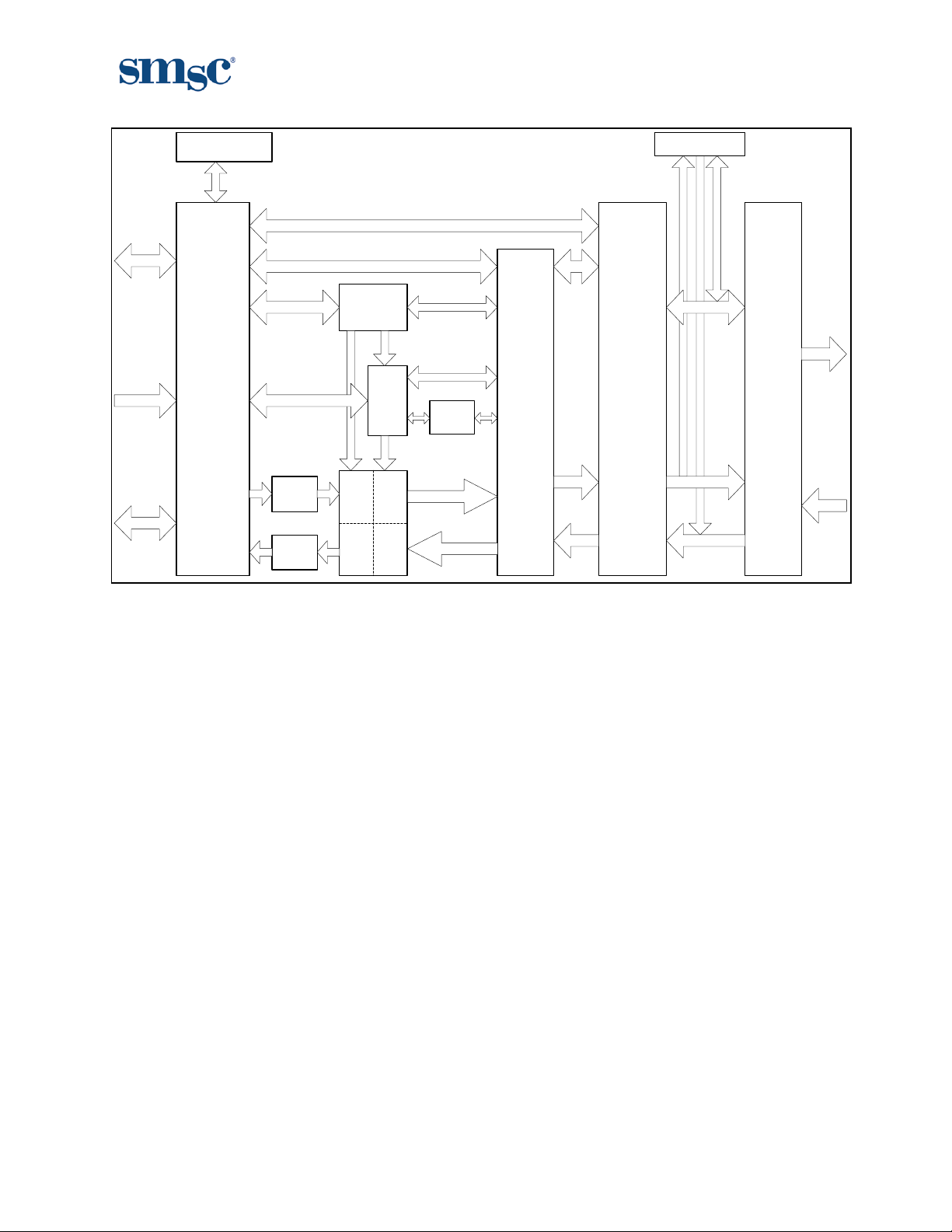
Chapter 3 Block Diagrams
The diagram shown in FIGURE 3 - BASIC FUNCTIONAL BLOCK DIAGRAM, describes the device basic
functional blocks. The SMSC LAN91C111 is a single chip solution for embedded designs with minimal
Host and external supporting devices required to implement 10/100 Ethernet connectivity solutions.
The optional Serial EEPROM is used to store information relating to default IO offset parameters as well as
which of the Interrupt line are used by the host.
LAN91C111
PHY
Core
Transformer
RJ45
ISA,Embedded
Processor
Ethernet
MAC
Internal IEEE 802.3 MII (Media
Independent Interface)
Host System
TX/RX Buffer (8K)
Serial
EEProm
(Optional)
Minimal LAN91C111
Configuration
FIGURE 3 - BASIC FUNCTIONAL BLOCK DIAGRAM
SMSC DS – LAN91C111 Rev. B Page 9 Rev. 09/17/2002
PRELIMINARY
10/100 Non-PCI Ethernet Single Chip MAC + PHY
EEPROM
INTERFACE
Control
MII
Control
Address
Data
8-32 bit
Bus
Interface
Unit
Control
Control
WR
FIFO
RD
FIFO
Control
Arbiter
MMU
8K Byte
Dynamically
Allocated
SRAM
TX/RX
FIFO
Pointer
32-bit Data
32-bit Data
DMA
Control
TX Data
RX Data
Ethernet
Protocol
Handler
(EPH)
Control
TPO
10/100
PHY
TXD[0-3]
TPI
RXD[0-3]
FIGURE 4 - BLOCK DIAGRAM
The diagram shown in FIGURE 4 describes the supported Host interfaces, which include ISA or Generic
Embedded. The Host interface is an 8, 16 or 32 bit wide address / data bus with extensions for 32, 16 and
8 bit embedded RISC and ARM processors.
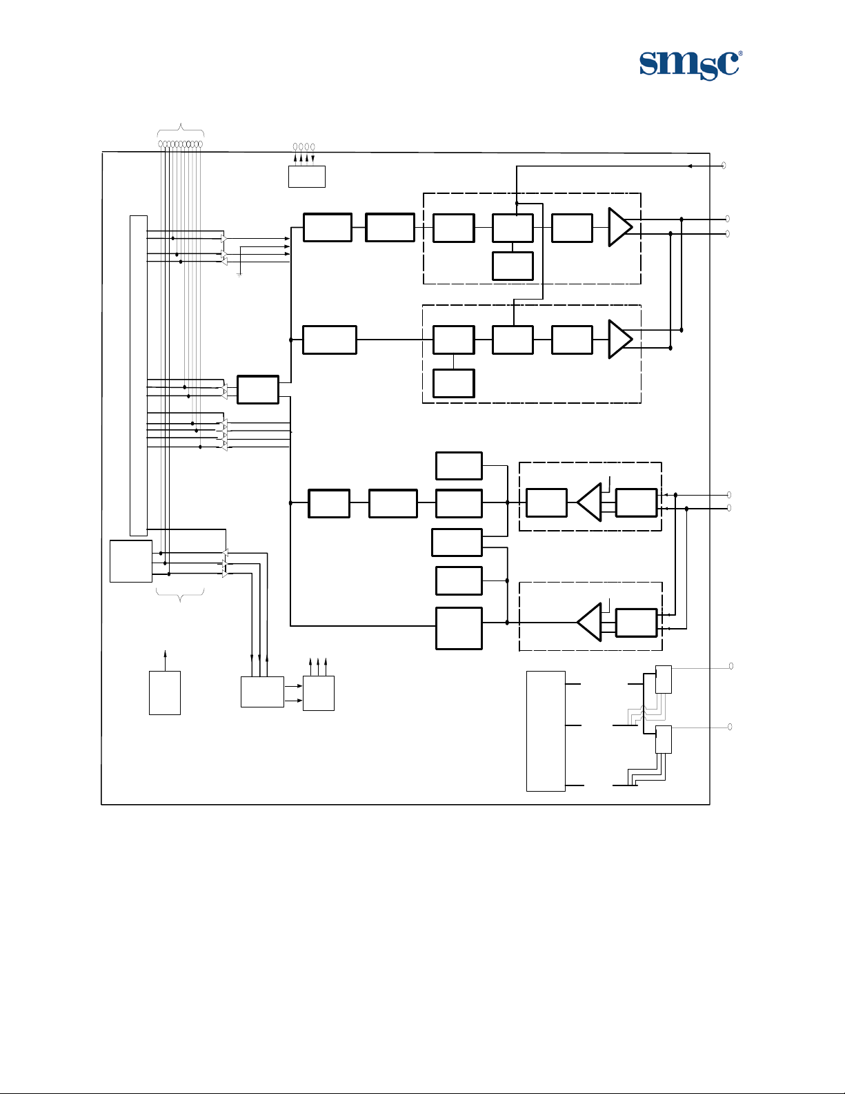
The figure shown next page describes the SMSC LAN91C111 functional blocks required to integrate a
10/100 Ethernet Physical layer framer to the internal MAC.
Rev. 09/17/2002 Page 10 SMSC DS – LAN91C111 Rev. B
PRELIMINARY
10/100 Non-PCI Ethernet Single Chip MAC + PHY
MII External
Signals
EECS
EESK
EEPROM
CONTROL
TXD[3:0]
TX_ER
TXEN100
TX25
EEDO
EEDI
S
A
B
I
R
X
T
-
E
B
A
S
0
0
1
T
E
R
T
I
S
M
A
N
R
T
I
T
W
C
H
D
E
5
B
B
4
D
R
O
E
N
E
C
E
R
A
M
B
L
R
S
C
L
M
O
N
E
C
0
B
A
1
S
A
N
R
T
S
3
T
D
R
E
T
-
S
E
T
T
I
M
R
R
N
E
T
C
U
R
C
E
O
U
S
C
K
L
O
C
E
N
G
L
)
P
L
(
E
R
P
L
E
T
L
I
F
+
-
R
+
O
P
T
-
P
O
T
MII
SERIAL
Manage
-ment
CSMA/CD
Power
Reset
On
MII
To MII External Signals
CRS100
COL100
RXD[3:0]
RX_ER
RX_DV
RX25
MDI
MCLK
MDO
L
I
O
L
C
PHY
CONTROLS
D
C
E
R
S
T
H
M
C
A
N
E
O
N
I
S
R
M
O
C
K
L
O
C
N
E
G
)
L
P
L
(
A
1
H
L
C
E
U
S
Q
&
C
K
L
O
4
D
C
E
AUTONEG
LOGIC
B
5
B
D
R
O
E
C
R
E
S
A
D
M
R
E
C
B
L
A
A
T
D
E
R
Y
O
E
V
C
R
T
U
O
A
T
O
I
I
A
T
O
N
E
N
G
K
&
N
L
I
H
L
C
U
S
E
Q
&
C
K
L
O
C
A
A
T
D
y
e
r
v
o
e
c
R
t
e
s
e
r
h
n
c
M
a
(
)
r
d
e
o
e
c
D
E
1
R
P
L
E
T
L
I
F
X
T
E
B
-
A
S
0
0
E
I
E
C
V
E
R
R
L
T
M
N
C
D
O
R
E
-
T
S
E
0
B
A
E
I
E
C
V
E
R
LED
Control
R
+
+
-
+
+
+
-
nPLED[0-5]
LS[2-0]A
+
-
h
t
V
-
+
/
P
I
T
V
E
P
T
I
A
A
D
R
L
U
I
E
A
Q
Z
E
h
V
t
-
/
P
L
E
R
T
L
I
F
Multiplex er
S
D
1
S
8
EN
C
C
1
3C2
B
Multiplex er
S
D
1
S
8
EN
C
C
1
3C2
B
+
P
I
T
-
LEDA
LEDB
LS[2-0]B
FIGURE 5 - LAN91C111 PHYSICAL LAYER TO INTERNAL MAC BLOCK DIAGRAM
SMSC DS – LAN91C111 Rev. B Page 11 Rev. 09/17/2002
PRELIMINARY

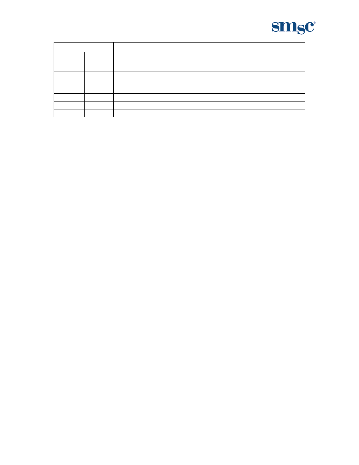
Chapter 4 Signal Descriptions
Table 1 - LAN91C111 Pin Requirements (128 Pin QFP and 1.0mm TQFP package)
FUNCTION PIN SYMBOLS NUMBER OF PINS
System Address Bus A1-A15, AEN, nBE0-nBE3 20
System Data Bus D0-D31 32
System Control Bus RESET, nADS, LCLK, ARDY,
nRDYRTN, nSRDY, INTR0,
nLDEV, nRD, nWR, nDATACS,
nCYCLE, W/nR, nVLBUS
Serial EEPROM EEDI, EEDO, EECS, EESK,
ENEEP, IOS0-IOS2
LEDs nLEDA, nLEDB 2
PHY TPO+, TPO-, TPI+, TPI-, nLNK,
LBK, nCNTRL, RBIAS
Crystal Oscillator XTAL1, XTAL2 2
Power VDD, AVDD 10
Ground GND, AGND 12
Physical Interface (MII) TXEN100, CRS100, COL100,
RX_DV, RX_ER, TXD0-TXD3,
RXD0-RXD3, MDI, MDO,
MCLK, RX25, TX25
MISC nCSOUT, X25OUT 2
TOTAL 128
10/100 Non-PCI Ethernet Single Chip MAC + PHY
14
8
8
18
Rev. 09/17/2002 Page 12 SMSC DS – LAN91C111 Rev. B
PRELIMINARY

10/100 Non-PCI Ethernet Single Chip MAC + PHY
Chapter 5 Description of Pin Functions
PIN NO.
TQFP QFP
81-92 83-94 Address A4-A15 I** Input. Decoded by LAN91C111 to
78-80 80-82 Address A1-A3 I** Input. Used by LAN91C111 for
41 43 Address
94-97 96-99 nByte Enable nBE0-
107-104,
102-99,
76-73, 7168, 66-63,
61-58, 5653, 51-48
30 32 Reset RESET IS** Input. When this pin is asserted
37 39 nAddress
35 37 nCycle nCYCLE I** Input. This active low signal is used
36 38 Write/
109-106,
104-101,
78-75,
73-70,
68-65,
63-60,
58-55,
53-50
NAME SYMBOL
AEN I** Input. Used as an address qualifier.
Enable
nBE3
Data Bus D0-D31 I/O24** Bidirectional. 32 bit data bus used to
nADS IS** Input. For systems that require
Strobe
W/nR IS** Input. Defines the direction of
nRead
BUFFER
TYPE
determine access to its registers.
internal register selection.
Address decoding is only enabled
when AEN is low.
I** Input. Used during LAN91C111
register accesses to determine the
width of the access and the
register(s) being accessed. nBE0nBE3 are ignored when nDATACS is
low (burst accesses) because 32 bit
transfers are assumed.
access the LAN91C111’s internal
registers. Data bus has weak
internal pullups. Supports direct
connection to the system bus without
external buffering. For 16 bit
systems, only D0-D15 are used.
high, the controller performs an
internal system (MAC & PHY) reset.
It programs all the registers to their
default value, the controller will read
the EEPROM device through the
EEPROM interface
input is not considered active unless
it is active for at least 100ns to filter
narrow glitches.
address latching, the rising edge of
nADS indicates the latching moment
for A1-A15 and AEN. All
LAN91C111 internal functions of A1A15, AEN are latched except for
nLDEV decoding.
to control LAN91C111 EISA burst
mode synchronous bus cycles.
synchronous cycles. Write cycles
when high, read cycles when low.
DESCRIPTION
(Note 5.1). This
SMSC DS – LAN91C111 Rev. B Page 13 Rev. 09/17/2002
PRELIMINARY

10/100 Non-PCI Ethernet Single Chip MAC + PHY
PIN NO.
TQFP QFP
40 42 nVL Bus
42
38 40
43 45 nSynchronous
46 48 nReady
29 31 Interrupt INTR0 O24 Interrupt Output – Used to interrupt the
45 47 nLocal Device nLDEV O16 Output. This active low output is
44 Local Bus
NAME SYMBOL
nVLBUS I with
Access
LCLK I** Input. Used to interface synchronous
Clock
Asynchronous
Ready
Ready
Return
ARDY OD16 Open drain output. ARDY may be
nSRDY O16 Output. This output is used when
nRDYRTN I** Input. This input is used to complete
BUFFER
TYPE
pullup**
DESCRIPTION
Input. When low, the LAN91C111
synchronous bus interface is
configured for VL Bus accesses.
Otherwise, the LAN91C111 is
configured for EISA DMA burst
accesses. Does not affect the
asynchronous bus interface.
buses. Maximum frequency is 50
MHz. Limited to 8.33 MHz for EISA
DMA burst mode. This pin should be
tied high if it is in asynchronous mode.
used when interfacing asynchronous
buses to extend accesses. Its rising
(access completion) edge is controlled
by the XTAL1 clock and, therefore,
asynchronous to the host CPU or bus
clock. ARDY is negated during
Asynchronous cycle when one of the
following conditions occurs:
1) No_Wait Bit in the Configuration
Register is cleared.
2) Read FIFO contains less than 4
bytes when read.
3) Write FIFO is full when write.
interfacing synchronous buses and
nVLBUS=0 to extend accesses. This
signal remains normally inactive, and
its falling edge indicates completion.
This signal is synchronous to the bus
clock LCLK.
synchronous read cycles. In EISA
burst mode it is sampled on falling
LCLK edges, and synchronous cycles
are delayed until it is sampled high.
Host on a status event. Note: The
selection bits used to determined by
the value of INT SEL 1-0 bits in the
Configuration Register are no longer
required and have been set to
reserved in this revision of the FEAST
family of devices.
asserted when AEN is low and A4-A15
decode to the LAN91C111 address
programmed into the high byte of the
Base Address Register. nLDEV is a
combinatorial decode of unlatched
address and AEN signals.
Rev. 09/17/2002 Page 14 SMSC DS – LAN91C111 Rev. B
PRELIMINARY

10/100 Non-PCI Ethernet Single Chip MAC + PHY
PIN NO.
TQFP QFP
31 33 nRead Strobe nRD IS** Input. Used in asynchronous bus
32 34 nWrite Strobe nWR IS** Input. Used in asynchronous bus
34 36 nData Path
9 11 EEPROM
10 12 EEPROM
7 9 EEPROM
8 10 EEPROM
3-5 5-7 I/O Base IOS0-
6 8 Enable
127, 128 1, 2 Crystal 1
1, 33, 44,
62, 77, 98,
110, 120
11, 16 13, 18 Analog Power AVDD +3.3V Analog power supply pins.
24, 39, 52,
57, 67, 72,
93, 103,
108, 117
13, 19 15, 21 Analog
21 23 Loopback LBK O4 Output. Active when LOOP bit is set
3, 35, 46,
64, 79,
100, 112,
122
26, 41,
54, 59,
69, 74,
95, 105,
110, 119
NAME SYMBOL
nDATACS I with
Chip Select
EESK O4
Clock
EECS O4 Output. Serial EEPROM chip select.
Select
EEDO O4 Output. Connected to the DI input of
Data Out
EEDI I with
Data In
IOS2
ENEEP I with
EEPROM
XTAL1
Crystal 2
Power VDD +3.3V Power supply pins.
Ground GND Ground pins.
Ground
XTAL2
AGND Analog Ground pins
BUFFER
TYPE
interfaces.
interfaces.
Input. When nDATACS is low, the
pullup**
pulldown
**
I with
pullup**
pullup**
Iclk** An external 25 MHz crystal is
Data Path can be accessed regardless
of the values of AEN, A1-A15 and the
content of the BANK SELECT
Register. nDATACS provides an
interface for bursting to and from the
LAN91C111 32 bits at a time.
Output. 4 µsec clock used to shift data
in and out of the serial EEPROM.
Used for selection and command
framing of the serial EEPROM.
the serial EEPROM.
Input. Connected to the DO output of
the serial EEPROM.
Input. External switches can be
connected to these lines to select
between predefined EEPROM
configurations.
Input. Enables (when high or open)
LAN91C111 accesses to the serial
EEPROM. Must be grounded if no
EEPROM is connected to the
LAN91C111.
connected across these pins. If a TTL
clock is supplied instead, it should be
connected to XTAL1 and XTAL2
should be left open. XTAL1 is the 5V
tolerant input of the internal amplifier
and XTAL2 is the output of the internal
amplifier.
(TCR bit 1).
DESCRIPTION
SMSC DS – LAN91C111 Rev. B Page 15 Rev. 09/17/2002
PRELIMINARY

10/100 Non-PCI Ethernet Single Chip MAC + PHY
PIN NO.
TQFP QFP
20 22 nLink Status nLNK I with
28 30 nCNTRL nCNTRL O12 General Purpose Control Pin
47 49 X25out X25out O12 25Mhz Output to external PHY
111 113 Transmit
119 121 Carrier Sense
125 127 Receive Data
112 114 Collision
113-116 115-118 Transmit Data TXD3-
109 111 Transmit
118 120 Receive Clock RX25 I with
121-124 123-126 Receive Data RXD3-
25 27 Management
NAME SYMBOL
TXEN100 O12 Output to MII PHY. Envelope to 100
Enable 100
Mbps
CRS100 I with
100 Mbps
RX_DV I with
Valid
COL100 I with
Detect 100
Mbps
TXD0
TX25 I with
Clock
RXD0
MDI I with
Data Input
BUFFER
TYPE
Input. General-purpose input port
pullup
pulldown
pulldown
pulldown
O12 Outputs. Transmit Data nibble to MII
pullup
pullup
I with
pullup
pulldown
used to convey LINK status (EPHSR
bit 14).
Mbps transmission.
Input from MII PHY. Envelope of
packet reception used for deferral and
backoff purposes.
Input from MII PHY. Envelope of data
valid reception. Used for receive data
framing.
Input from MII PHY. Collision
detection input.
PHY.
Input. Transmit clock input from MII.
Nibble rate clock (25MHz for 100Mbps
& 2.5MHz for 10Mbps).
Input. Receive clock input from MII
PHY. Nibble rate clock. (25MHz for
100Mbps & 2.5MHz for 10Mbps).
Inputs. Received Data nibble from MII
PHY.
MII management data input.
DESCRIPTION
26 28 Management
Data Output
27 29 Management
Clock
126 128 Receive Error RX_ER I with
2 4 nChip Select
Output
12 14 External
Resistor
Rev. 09/17/2002 Page 16 SMSC DS – LAN91C111 Rev. B
MDO O4 MII management data output.
MCLK O4 MII management clock.
Input. Indicates a code error detected
pulldown
nCSOUT O4 Output. Chip Select provided for
RBIAS NA Transmit Current Set. An external
by PHY. Used by the LAN91C111 to
discard the packet being received.
The error indication reported for this
event is the same as a bad CRC
(Receive Status Word bit 13).
mapping of PHY functions into
LAN91C111 decoded space. Active on
accesses to LAN91C111’s eight lower
addresses when the BANK
SELECTED is 7.
resistor connected between this pin
and GND will set the output current for
the TP transmit outputs
PRELIMINARY
10/100 Non-PCI Ethernet Single Chip MAC + PHY
PIN NO.
NAME SYMBOL
TQFP QFP
14 16 TPO+ O/I Twisted Pair Transmit Output, Positive.
15 17 TPO- O/I Twisted Pair Transmit Output,
17 19 TPI+ I/O Twisted Pair Receive Input, Positive
18 20 TPI- I/O Twisted Pair Receive Input, Negative.
22 24 nLEDA OD24 PHY LED Output
23 25 nLEDB OD24 PHY LED Output
Note 5.1 If the EEPROM is enabled.
BUFFER
TYPE
DESCRIPTION
Negative
SMSC DS – LAN91C111 Rev. B Page 17 Rev. 09/17/2002
PRELIMINARY

10/100 Non-PCI Ethernet Single Chip MAC + PHY
Chapter 6 Signal Description Parameters
This section provides a detailed description of each SMSC LAN91C111 signal. The signals are arranged in
functional groups according to their associated function.
The ‘n’ symbol at the beginning of a signal name indicates that it is an active low signal. When ‘n’ is not
present before the signal name, it indicates an active high signal.
The term “assert” or “assertion” indicates that a signal is active; independent of whether that level is
represented by a high or low voltage. The term negates or negation indicates that a signal is inactive.
The term High-Z means tri-stated.
The term Undefined means the signal could be high, low, tri-stated, or in some in-between level.
6.1 Buffer Types
O4 Output buffer with 2mA source and 4mA sink
O12 Output buffer with 6mA source and 12mA sink
O16 Output buffer with 8mA source and 16mA sink
O24 Output buffer with 12mA source and 24mA sink
OD16 Open drain buffer with 16mA sink
OD24 Open drain buffer with 24mA sink
I/O4 Bidirectional buffer with 2mA source and 4mA sink
I/O24 Bidirectional buffer with 12mA source and 24mA sink
I/OD Bidirectional Open drain buffer with 4mA sink
I Input buffer
IS Input buffer with Schmitt Trigger Hysteresis
Iclk Clock input buffer
I/O Differential Input
O/I Differential Output
** 5V tolerant. Input pins are able to accept 5V signals
DC levels and conditions defined in the DC Electrical Characteristics section
Rev. 09/17/2002 Page 18 SMSC DS – LAN91C111 Rev. B
PRELIMINARY

10/100 Non-PCI Ethernet Single Chip MAC + PHY
Chapter 7 Functional Description
7.1 Clock Generator Block
1) The XTAL1 and XTAL2 pins are to be connected to a 25 MHz crystal.
2) TX25 is an input clock. It will be the nibble rate of the particular PHY connected to the MII (2.5 MHz for a
10 Mbps PHY, and 25 MHz for a 100 Mbps PHY).
3) RX25 - This is the MII nibble rate receive clock used for sampling received data nibbles and running the
receive state machine. (2.5 MHz for a 10 Mbps PHY, and 25 MHz for a 100 Mbps PHY).
4) LCLK - Bus clock - Used by the BIU for synchronous accesses. Maximum frequency is 50 MHz for VL
BUS mode, and 8.33 MHz for EISA slave DMA.
7.2 CSMA/CD Block
This is a 16 bit oriented block, with fully- independent Transmit and Receive logic. The data path in and out
of the block consists of two 16-bit wide uni-directional FIFOs interfacing the DMA block. The DMA port of
the FIFO stores 32 bits to exploit the 32 bit data path into memory, but the FIFOs themselves are 16 bit
wide. The Control Path consists of a set of registers interfaced to the CPU via the BIU.
7.2.1 DMA Block
This block accesses packet memory on the CSMA/CD’s behalf, fetching transmit data and storing received
data. It interfaces the CSMA/CD Transmit and Receive FIFOs on one side and the Arbiter block on the
other. To increase the bandwidth into memory, a 50 MHz clock is used by the DMA block, and the data
path is 32 bits wide.
For example, during active reception at 100 Mbps, the CSMA/CD block will write a word into the Receive FIFO
every 160ns. The DMA will read the FIFO and accumulate two words on the output port to request a memory
cycle from the Arbiter every 320ns.
The DMA machine is able to support full duplex operation. Independent receive and transmit counters are used.
Transmit and receive cycles are alternated when simultaneous receive and transmit accesses are needed.
7.2.2 Arbiter Block
The Arbiter block sequences accesses to packet RAM requested by the BIU and by the DMA blocks. BIU
requests represent pipelined CPU accesses to the Data Register, while DMA requests represent
CSMA/CD data movement.
Internal SRAM read accesses are always 32 bit wide, and the Arbiter steers the appropriate byte(s) to the
appropriate lanes as a function of the address.
The CPU Data Path consists of two uni-directional FIFOs mapped at the Data Register location. These
FIFOs can be accessed in any combination of bytes, word, or doublewords. The Arbiter will indicate 'Not
Ready' whenever a cycle is initiated that cannot be satisfied by the present state of the FIFO.
SMSC DS – LAN91C111 Rev. B Page 19 Rev. 09/17/2002
PRELIMINARY

7.3 MMU Block
The Hardware Memory Management Unit allocates memory and transmit and receive packet queues. It
also determines the value of the transmit and receive interrupts as a function of the queues. The page size
is 2048 bytes, with a maximum memory size of 8kbytes. MIR values are interpreted in 2048 byte units.
7.4 BIU Block
The Bus Interface Unit can handle synchronous as well as asynchronous buses; different signals are used
for each one. Transparent latches are added on the address path using rising nADS for latching.
When working with an asynchronous bus like ISA, the read and write operations are controlled by the
edges of nRD and nWR. ARDY is used for notifying the system that it should extend the access cycle. The
leading edge of ARDY is generated by the leading edge of nRD or nWR while the trailing edge of ARDY is
controlled by the internal LAN91C111 clock and, therefore, asynchronous to the bus.
In the synchronous VL Bus type mode, nCYCLE and LCLK are used to for read and write operations.
Completion of the cycle may be determined by using nSRDY. nSRDY is controlled by LCLK and
synchronous to the bus.
Direct 32 bit access to the Data Path is supported by using the nDATACS input. By asserting nDATACS,
external DMA type of devices will bypass the BIU address decoders and can sequentially access memory
with no CPU intervention. nDATACS accesses can be used in the EISA DMA burst mode (nVLBUS=1) or
in asynchronous cycles. These cycles MUST be 32 bit cycles. Please refer to the corresponding timing
diagrams for details on these cycles.
10/100 Non-PCI Ethernet Single Chip MAC + PHY
The BIU is implemented using the following principles:
a) Address decoding is based on the values of A15-A4 and AEN.
b) Address latching is performed by using transparent latches that are transparent when nADS=0 and
nRD=1, nWR=1 and latch on nADS rising edge.
c) Byte, word and doubleword accesses to all registers and Data Path are supported except a
doubleword write to offset Ch will only write the BANK SELECT REGISTER (offset 0x0Fh).
d) No bus byte swapping is implemented (no eight bit mode).
e) Word swapping as a function of A1 is implemented for 16 bit bus support.
f) The asynchronous interface uses nRD and nWR strobes. If necessary, ARDY is negated on the
leading edge of the strobe. The ARDY trailing edge is controlled by CLK.
g) The VLBUS synchronous interface uses LCLK, nADS, and W/nR as defined in the VESA specification
as well as nCYCLE to control read and write operations and generate nSRDY.
h) EISA burst DMA cycles to and from the DATA REGISTER are supported as defined in the EISA Slave
Mode "C" specification when nDATACS is driven by nDAK.
i) Synchronous and asynchronous cycles can be mixed as long as they are not active simultaneously.
j) Address and bank selection can be bypassed to generate 32 bit Data Path accesses by activating the
nDATACS pin.
7.5 MAC-PHY Interface
The LAN91C111 integrates the IEEE 802.3 Physical Layer (PHY) and Media Access Control (MAC) into
the same silicon. The data path connection between the MAC and the internal PHY is provided by the
internal MII. The LAN91C111 also supports the EXT_PHY mode for the use of an external PHY, such as
HPNA. This mode isolates the internal PHY to allow interface with an external PHY through the MII pins.
To enter this mode, set EXT PHY bit to 1 in the Configuration Register.
Rev. 09/17/2002 Page 20 SMSC DS – LAN91C111 Rev. B
PRELIMINARY

10/100 Non-PCI Ethernet Single Chip MAC + PHY
7.5.1 Management Data Software Implementation
The MII interface contains of a pair of signals that physically transport the management information across
the MII, a frame format and a protocol specification for exchanging management frames, and a register set
that can be read and written using these frames. MII management refers to the ability of a management
entity to communicate with PHY via the MII serial management interface (MI) for the purpose of displaying,
selecting and/or controlling different PHY options. The host manipulates the MAC to drive the MII
management serial interface. By manipulating the MAC's registers, MII management frames are
generated on the management interface for reading or writing information from the PHY registers. Timing
and framing for each management command is to be generated by the CPU (host).
The MAC and external PHY communicate via MDIO and MDC of the MII Management serial interface.
MDIO: Management Data input/output. Bi-directional between MAC and PHY that carries management
data. All control and status information sent over this pin is driven and sampled synchronously
to the rising edge of MDC signal.
MDC: Management Data Clock. Sourced by the MAC as a timing reference for transfer of information
on the MDIO signal. MDC is a periodic signal with no maximum high or low times. The
minimum high and low times should be 160ns each and the minimum period of the signal
should be 400ns. These values are regardless of the nominal period of the TX and RX clocks.
7.5.2 Management Data Timing
A timing diagram for a Ml serial port frame is shown in FIGURE 6. The Ml serial port is idle when at least
32 continuous 1's are detected on MDIO and remains idle as long as continuous 1's are detected. During
idle, MDIO is in the high impedance state. When the Ml serial port is in the idle state, a 01 pattern on the
MDIO initiates a serial shift cycle. Data on MDIO is then shifted in on the next 14 rising edges of MDC
(MDIO is high impedance). If the register access mode is not enabled, on the next 16 rising edges of
MDC, data is either shifted in or out on MDIO, depending on whether a write or read cycle was selected
with the bits READ and WRITE. After the 32 MDC cycles have been completed, one complete register
has been read/written, the serial shift process is halted, data is latched into the device, and MDIO goes
into high impedance state. Another serial shift cycle cannot be initiated until the idle condition (at least 32
continuous 1's) is detected.
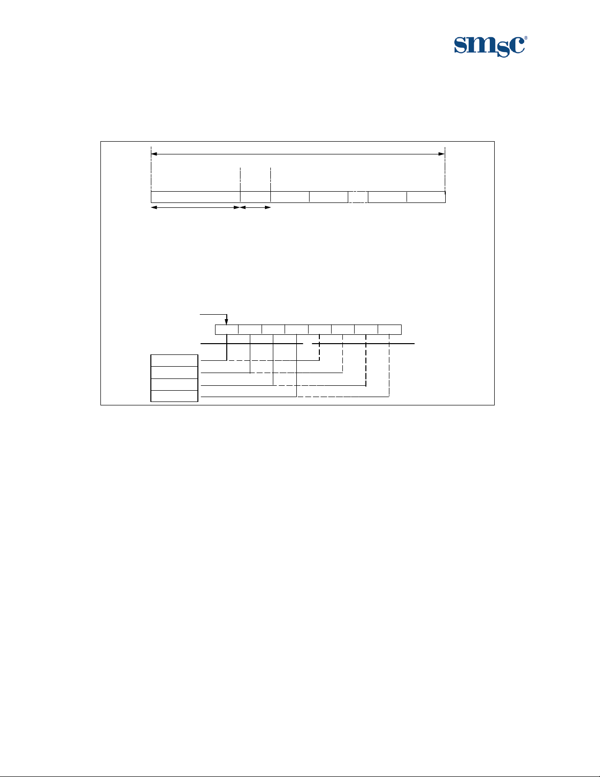
7.5.3 MI Serial Port Frame Structure
The structure of the PHY serial port frame is shown in Table 5 and timing diagram of a frame is shown in
FIGURE 6. Each serial port access cycle consists of 32 bits (or 192 bits if multiple register access is
enabled and REGAD[4:0]=11111), exclusive of idle. The first 16 bits of the serial port cycle are always
write bits and are used for addressing. The last 16/176 bits are from one/all of the 11 data registers.
The first 2 bit in Table 5 and FIGURE 6 are start bits and need to be written as a 01 for the serial port cycle
to continue. The next 2 bits are a read and write bit which determine if the accessed data register bits will
be read or write. The next 5 bits are device addresses. The next 5 bits are register address select bits,
which select one of the five data registers for access. The next 1 bit is a turnaround bit which is not an
actual register bit but extra time to switch MDIO from write to read if necessary, as shown in FIGURE 6.
The final 16 bits of the PHY Ml serial port cycle (or 176 bits if multiple register access is enabled and
REGAD[4:0]=11111) come from the specific data register designated by the register address bits
REGAD[4:0].
SMSC DS – LAN91C111 Rev. B Page 21 Rev. 09/17/2002
PRELIMINARY
10/100 Non-PCI Ethernet Single Chip MAC + PHY
1
3
0
3
9
2
8
2
7
2
6
2
5
2
4
2
3
2
2
2
1
2
0
2
9
1
8
1
7
1
6
1
5
1
4
1
3
1
2
1
1
1
0
1
9
8
7
6
5
4
3
2
1
E
0
L
C
Y
C
E
T
I
R
W
C
D
M
0
D
1
D
2
D
3
D
4
D
5
D
6
D
7
]
D
0
:
5
1
[
A
8
T
D
A
D
9
D
0
1
D
1
1
D
2
1
D
3
1
D
4
1
D
5
1
D
]
0
0
:
1
[
A
T
1
0
R
1
R
]
0
:
4
[
2
D
R
A
G
E
R
3
R
4
R
0
P
1
P
]
0
:
4
[
D
2
A
P
Y
H
P
3
P
4
P
1
]
0
:
1
[
P
O
0
1
]
0
:
1
[
T
S
0
O
I
D
M
C
D
M
F
O
S
E
G
D
E
G
N
I
S
I
E
R
S
T
I
T
N
I
R
O
B
W
A
T
A
D
N
I
S
K
C
O
L
C
Y
H
P
1
3
0
3
9
2
8
2
7
2
6
2
5
2
4
2
3
2
2
2
1
2
0
2
9
1
8
1
7
1
6
1
5
1
4
1
3
1
2
1
1
1
0
1
9
8
7
6
5
4
3
2
1
0
E
L
C
Y
C
D
A
E
R
C
D
M
0
D
1
D
2
D
3
D
4
D
5
D
6
D
7
D
]
0
:
5
8
1
[
D
A
T
A
D
9
D
0
1
D
1
1
D
2
1
D
3
1
D
4
1
D
5
1
D
0
]
0
:
1
[
A
T
Z
0
R
1
]
0
R
:
4
[
D
A
2
G
R
E
R
3
R
4
R
0
P
1
P
]
0
:
4
[
2
D
P
A
Y
H
P
3
P
4
P
0
]
0
:
1
[
P
O
1
1
]
0
:
1
[
T
S
0
O
I
D
M
C
D
M
F
O
S
E
G
D
E
G
N
I
S
S
I
T
R
I
B
N
D
O
A
A
E
T
R
A
D
T
U
O
S
K
C
O
L
C
Y
H
P
C
D
M
F
O
S
E
G
D
E
G
N
I
S
I
E
R
S
T
I
T
N
I
R
B
O
W
A
T
A
D
N
I
S
K
C
O
L
C
Y
H
P
FIGURE 6 - MI SERIAL PORT FRAME TIMING DIAGRAM
Rev. 09/17/2002 Page 22 SMSC DS – LAN91C111 Rev. B
PRELIMINARY
10/100 Non-PCI Ethernet Single Chip MAC + PHY
7.5.4 MII Packet Data Communication with External PHY
The MIl is a nibble wide packet data interface defined in IEEE 802.3. The LAN91C111 meets all the MIl
requirements outlined in IEEE 802.3 and shown in FIGURE 7.
OF
SFD
2 BT
TX_EN = 1
DATA 1
DATA NIBBLES
DATA 2
DATA N-1 DATA N
TX_EN = 0
IDLE
PREAMBLE
PRMBLE
62 BT
START
FRAME
DELIM.
TX_EN = 0
IDLE
= [ 1 0 1 0 ... ] 62 BITS LONG
= [ 1 1 ]
SFD
= [ BETWEEN 64-1518 DATA BYTES ]
DATAn
IDLE = TX_EN = 0
MAC's SERIAL BIT STREAM
MSB
SECOND
NIBBLE
MII
NIBBLE
STREAM
FIRST BIT
FIRST
NIBBLE
TXD0 / RXD0
TXD1 / RXD1
TXD2 / RXD2
TXD3 / RXD3
PREAMBLE
D0 D1 D2 D3 D4 D5 D6 D7
LSB
FIGURE 7 - MII FRAME FORMAT & MII NIBBLE ORDER
The Mll consists of the following signals: four transmit data bits (TXD[3:0]), transmit clock (TX25),transmit
enable (TXEN100), four receive data bits(RXD[3:0]), receive clock(RX25), carrier sense (CRS100), receive
data valid (RX_DV), receive data error (RX_ER), and collision (COL100). Transmit data is clocked out using
the TX25 clock input, while receive data is clocked in using RX25. The transmit and receive clocks operate at
25 MHz in 100Mbps mode and 2.5 MHz in 10Mbps.
In 100 Mbps mode, the LAN91C111 provides the following interface signals to the PHY:
For transmission: TXEN100, TXD0-3, TX25
For reception: RX_DV, RX_ER, RXD0-3, RX25
For CSMA/CD state machines: CRS100, COL100
A transmission begins by TXEN100 going active (high), and TXD0-TXD3 having the first valid preamble
nibble. TXD0 carries the least significant bit of the nibble (that is the one that would go first out of the EPH
at 100 Mbps), while TXD3 carries the most significant bit of the nibble. TXEN100 and TXD0-TXD3 are
clocked by the LAN91C111 using TX25 rising edges. TXEN100 goes inactive at the end of the packet on
the last nibble of the CRC.
During a transmission, COL100 might become active to indicate a collision. COL100 is asynchronous to
the LAN91C111’s clocks and will be synchronized internally to TX25.
Reception begins when RX_DV (receive data valid) is asserted. A preamble pattern or flag octet will be present
at RXD0-RXD3 when RX_DV is activated. The LAN91C111 requires no training sequence beyond a full flag
octet for reception. RX_DV as well as RXD0-RXD3 are sampled on RX25 rising edges. RXD0 carries the least
SMSC DS – LAN91C111 Rev. B Page 23 Rev. 09/17/2002
PRELIMINARY

significant bit and RXD3 the most significant bit of the nibble. RX_DV goes inactive when the last valid nibble of
the packet (CRC) is presented at RXD0-RXD3.
RX_ER might be asserted during packet reception to signal the LAN91C111 that the present receive packet is
invalid. The LAN91C111 will discard the packet by treating it as a CRC error.
RXD0-RXD3 should always be aligned to packet nibbles, therefore, opening flag detection does not consider
misaligned cases. Opening flag detection expects the 5Dh pattern and will not reject the packet on nonpreamble patterns.
CRS100 is used as a frame envelope signal for the CSMA/CD MAC state machines (deferral and backoff
functions), but it is not used for receive framing functions. CRS100 is an asynchronous signal and it will be
active whenever there is activity on the cable, including LAN91C111 transmissions and collisions.
7.6 Serial EEPROM Interface
This block is responsible for reading the serial EEPROM upon hardware reset (or equivalent command)
and defining defaults for some key registers. A write operation is also implemented by this block, that
under CPU command will program specific locations in the EEPROM. This block is an autonomous state
machine and controls the internal Data Bus of the LAN91C111 during active operation.
10/100 Non-PCI Ethernet Single Chip MAC + PHY
7.7 Internal Physical Layer
The LAN91C111 integrates the IEEE 802.3 physical layer (PHY) internally. The EXT PHY bit in the
Configuration Register is 0 as the default configuration to set the internal PHY enabled. The internal PHY
address is 00000, the driver must use this address to talk to the internal PHY. The internal PHY is placed
in isolation mode at power up and reset. It can be removed from isolation mode by clearing the MII_DIS
bit in the PHY Control Register. If necessary, the internal PHY can be enabled by clearing the EXT_PHY
bit in the Configuration Register.
The internal PHY of LAN91C111 has nine main sections: controller interface, encoder, decoder, scrambler,
descrambler, clock and data recovery, twisted pair transmitter, twisted pair receiver, and MI serial port.
The LAN91C111 can operate as a 100BASE-TX device (hereafter referred to as 100Mbps mode) or as a
10BASE-T device (hereafter referred to as 10Mbps mode). The difference between the 100Mbps mode
and the 10Mbps mode is data rate, signaling protocol, and allowed wiring. The 100Mbps TX mode uses
two pairs of category 5 or better UTP or STP twisted pair cable with 4B5B encoded, scrambled, and MLT-3
coded 62.5 MHz ternary data to achieve a throughput of 100Mbps. The 10Mbps mode uses two pairs of
category 3 or better UTP or STP twisted pair cable with Manchester encoded, 10MHz binary data to
achieve a 10Mbps throughput. The data symbol format on the twisted pair cable for the 100 and 10Mbps
modes are defined in IEEE 802.3 specifications and shown in FIGURE 8.
Rev. 09/17/2002 Page 24 SMSC DS – LAN91C111 Rev. B
PRELIMINARY
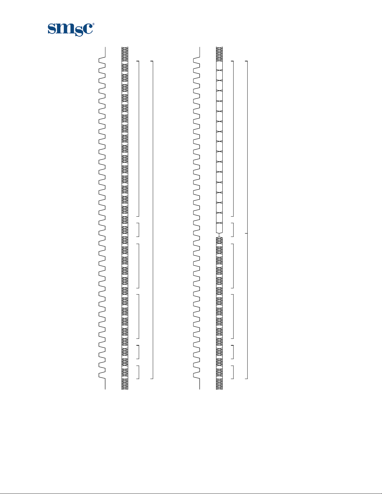
10/100 Non-PCI Ethernet Single Chip MAC + PHY
INTERFRAME
GAP
IDLE
IDLE
PREAMBLE
SSD
DA, SA, LN, LLC DATA, FCS
PREAMBLE
PREAMBLE
DA, SA, LN, LLC DATA, FCS
PREAMBLE
IDLE
PREAMBLE
SFD
= [ 1 1 ] WITH NO MID BIT TRANSITION
SOI
ETHERNET MAC
FRAME
SFD DA
100 BASE-TX DATA SYMBOLS
SFD
IDLE
SSD
= [ 1 1 0 0 0 1 0 0 0 1]
= [ 1 0 1 0 ...] 62 BITS LONG
= [ 1 1]
SFD
= [ DATA]
= [ 0 1 1 0 1 0 0 1 1 1]
ESD
10 BASE-T DATA SYMBOLS
SFD
= [ NO TRANSITIONS]
= [ 1 0 1 0 ... ] 62 BITS LONG
= [ 1 1]
= [ DATA]
DA
= [ 1 1 1 1...]
DA
SA
SA
SA
LN
LLC DATA
LN ESD
LLC DATA
BEFORE / AFTER
4B5B ENCODING,
SCRAMBLING,
AND MLT3
CODING
LN
LLC DATA
BEFORE / AFTER
MANCHESTER
ENCODING
FCS
FCS
FCS
SOI
INTERFRAME
GAP
IDLE
IDLE
FIGURE 8 - TX/10BT FRAME FORMAT
On the transmit side for 100Mbps TX operation, data is received on the controller and then sent to the
4B5B encoder for formatting. The encoded data is then sent to the scrambler. The scrambled and
encoded data is then sent to the TP transmitter. The TP transmitter converts the encoded and scrambled
data into MLT-3 ternary format, reshapes the output, and drives the twisted pair cable.
On the receive side for 100Mbps TX operation, the twisted pair receiver receives incoming encoded and
scrambled MLT-3 data from the twisted pair cable, remove any high frequency noise, equalizes the input
signal to compensate for the effects of the cable, qualifies the data with a squelch algorithm, and converts
the data from MLT-3 coded twisted pair levels to internal digital levels. The output of the twisted pair
receiver then goes to a clock and data recovery block which recovers a clock from the incoming data, uses
the clock to latch in valid data into the device, and converts the data back to NRZ format. The NRZ data is
SMSC DS – LAN91C111 Rev. B Page 25 Rev. 09/17/2002
PRELIMINARY

then unscrambled and decoded by the 4B5B decoder and descrambler, respectively, and outputted to the
Ethernet controller.
10Mbps operation is similar to the 100Mbps TX operation except, (1) there is no scrambler/descrambler,
(2) the encoder/decoder is Manchester instead of 4B5B, (3) the data rate is 10Mbps instead of 100Mbps,
and (4) the twisted pair symbol data is two level Manchester instead of ternary MLT-3.
The Management Interface, (hereafter referred to as the MI serial port), is a two pin bi-directional link
through which configuration inputs can be set and status outputs can be read. Each block plus the
operating modes are described in more detail in the following sections.
7.7.1 MII Disable
The internal PHY MII interface can be disabled by setting the MII disable bit in the MI serial port Control
register. When the MII is disabled, the MII inputs are ignored, the MII outputs are placed in high
impedance state, and the TP output is high impedance.
7.7.2 Encoder
4B5B Encoder - 100 Mbps
10/100 Non-PCI Ethernet Single Chip MAC + PHY
100BASE-TX requires that the data be 4B5B encoded. 4B5B coding converts the 4-Bit data nibbles into 5Bit date code words. The mapping of the 4B nibbles to the 5B code words is specified in IEEE 802.3. The
4B5B encoder on the LAN91C111 takes 4B nibbles from the controller interface, converts them into 5B
words and sends the 5B words to the scrambler. The 4B5B encoder also substitutes the first 8 bits of the
preamble with the SSD delimiters (a.k.a. /J/K/ symbols) and adds an ESD delimiter (a.k.a. MR/ symbols) to
the end of every packet, as defined in IEEE 802.3. The 4B5B encoder also fills the period between
packets, called the idle period, with the continuous stream of idle symbols.
Manchester Encoder - 10 Mbps
The Manchester encoding process combines clock and NRZ data such that the first half of the data bit
contains the complement of the data, and the second half of the data bit contains the true data, as
specified in IEEE 802.3. This guarantees that a transition always occurs in the middle of the bit call. The
Manchester encoder on the LAN91C111 converts the 10Mbps NRZ data from the controller interface into a
Manchester Encoded data stream for the TP transmitter and adds a start of idle pulse (SOI) at the end of
the packet as specified in IEEE 802.3. The Manchester encoding process is only done on actual packet
data, and the idle period between packets is not Manchester encoded and filled with link pulses.
7.7.3 Decoder
4B5B Decoder - 100 Mbps
Since the TP input data is 4B5B encoded on the transmit side, it must also be decoded by the 4B5B
decoder on the receive side. The mapping of the 5B nibbles to the 4B code words is specified in IEEE
802.3. The 4B5B decoder on the LAN91C111 takes the 5B code words from the descrambler, converts
them into 4B nibbles per Table 2, and sends the 4B nibbles to the controller interface. The 4B5B decoder
also strips off the SSD delimiter (a.k.a. /J/K/ symbols) and replaces them with two 4B Data 5 nibbles (a.k.a.
/5/ symbol), and strips off the ESD delimiter (a.k.a. /T/R/ symbols) and replaces it with two 4B Data 0
nibbles (a.k.a. /I/symbol), per IEEE 802.3 specifications and shown in FIGURE 8.
Rev. 09/17/2002 Page 26 SMSC DS – LAN91C111 Rev. B
PRELIMINARY

10/100 Non-PCI Ethernet Single Chip MAC + PHY
SYMBOL NAME DESCRIPTION 5B CODE 4B CODE
0 Data 0 11110 0000
1 Data 1 01001 0001
2 Data 2 10100 0010
3 Data 3 10101 0011
4 Data 4 01010 0100
5 Data 5 01011 0101
6 Data 6 01110 0110
7 Data 7 01111 0111
8 Data 8 10010 1000
9 Data 9 10011 1001
A Data A 10110 1010
B Data B 10111 1011
C Data C 11010 1100
D Data D 11011 1101
E Data E 11100 1110
F Data F 11101 1111
I Idle 11111 0000
J SSD #1 11000 0101
K SSD #2 10001 0101
T ESD #1 01101 0000
R ESD #2 00111 0000
H Halt 00100 Undefined
--- Invalid codes All others* 0000*
Table 2 - 4B/5B Symbol Mapping
* These 5B codes are not used. For decoder, these 5B codes are decoded to 4B 0000. For encoder, 4B
0000 is encoded to 5B 11110, as shown in symbol Data 0.
The 4B5B decoder detects SSD, ESD and codeword errors in the incoming data stream as specified in
IEEE 802.3. These errors are indicated by asserting RX_ER output while the errors are being transmitted
across RXD[3:0], and they are also indicated in the serial port by setting SSD, ESD, and codeword error
bits in the PHY MI serial port Status Output register.
Manchester Decoder - 10 Mbps
In Manchester coded data, the first half of the data bit contains the complement of the data, and the
second half of the data bit contains the true data. The Manchester decoder in the LAN91C111 converts
the Manchester encoded data stream from the TP receiver into NRZ data for the controller interface by
decoding the data and stripping off the SOI pulse. Since the clock and data recovery block has already
separated the clock and data from the TP receiver, the Manchester decoding process to NRZ data is
inherently performed by that block.
7.7.4 Clock and Data Recovery
Clock Recovery - 100 Mbps
Clock recovery is done with a PLL. If there is no valid data present on the TP inputs, the PLL is locked to
the 25 MHz TX25. When valid data is detected on the TP inputs with the squelch circuit and when the
adaptive equalizer has settled, the PLL input is switched to the incoming data on the TP input. The PLL
then recovers a clock by locking onto the transitions of the incoming signal from the twisted pair wire. The
SMSC DS – LAN91C111 Rev. B Page 27 Rev. 09/17/2002
PRELIMINARY

10/100 Non-PCI Ethernet Single Chip MAC + PHY
recovered dock frequency is a 25 MHz nibble dock, and that clock is outputted on the controller interface
signal RX25.
Data Recovery - 100 Mbps
Data recovery is performed by latching in data from the TP receiver with the recovered clock extracted by
the PLL. The data is then converted from a single bit stream into nibble wide data word according to the
format shown in FIGURE 7.
Clock Recovery - 10 Mbps
The clock recovery process for 10Mbps mode is identical to the 100Mbps mode except, (1) the recovered
clock frequency is 2.5 MHz nibble clock, (2) the PLL is switched from TX25 to the TP input when the
squelch indicates valid data, (3) The PLL takes up to 12 transitions (bit times) to lock onto the preamble, so
some of the preamble data symbols are lost, but the dock recovery block recovers enough preamble
symbols to pass at least 6 nibbles of preamble to the receive controller interface as shown in FIGURE 7.
Data Recovery - 10 Mbps
The data recovery process for 10Mbps mode is identical to the 100Mbps mode. As mentioned in the
Manchester Decoder section, the data recovery process inherently performs decoding of Manchester
encoded data from the TP inputs.
7.7.5 Scrambler
100 Mbps
100BASE-TX requires scrambling to reduce the radiated emissions on the twisted pair. The LAN91C111
scrambler takes the encoded data from the 4B5B encoder, scrambles it per the IEEE 802.3 specifications,
and sends it to the TP transmitter.
10 Mbps
A scrambler is not used in 10Mbps mode.
Scrambler Bypass
The scrambler can be bypassed by setting the bypass scrambler/descrambler bit in the PHY Ml serial port
Configuration 1 register. When this bit is set, the 5B data bypasses the scrambler and goes directly from
the 4B5B encoder to the twisted pair transmitter.
7.7.6 Descrambler
100 Mbps
The LAN91C111 descrambler takes the scrambled data from the data recovery block, descrambles it per
the IEEE 802.3 specifications, aligns the data on the correct 5B word boundaries, and sends it to the 4B5B
decoder.
The algorithm for synchronization of the descrambler is the same as the algorithm outlined in the IEEE
802.3 specification. Once the descrambler is synchronized, it will maintain synchronization as long as
enough descrambled idle pattern 1's are detected within a given interval. To stay in synchronization, the
descrambler needs to detect at least 25 consecutive descrambled idle pattern 1's in a 1ms interval. If 25
Rev. 09/17/2002 Page 28 SMSC DS – LAN91C111 Rev. B
PRELIMINARY

10/100 Non-PCI Ethernet Single Chip MAC + PHY
consecutive descrambled idle pattern 1's are not detected within the 1ms interval, the descrambler goes
out of synchronization and restarts the synchronization process.
If the descrambler is in the unsynchronized state, the descrambler loss of synchronization detect bit is set
in the Ml serial port Status Output register to indicate this condition. Once this bit is set, it will stay set until
the descrambler achieves synchronization.
10 Mbps
A descrambler is not used in 10 Mbps mode.
Descrambler Bypass
The descrambler can be bypassed by setting the bypass scrambler/descrambler bit in the PHY MI serial
port Configuration 1 register. When this bit is set, the data bypasses the descrambler and goes directly
from the TP receiver to the 4B5B decoder.
7.7.7 Twisted Pair Transmitter
Transmitter - 100 Mbps
The TX transmitter consists of MLT-3 encoder, waveform generator and line driver.
The MLT-3 encoder converts the NRZ data from the scrambler into a three level MLT-3 code required by
IEEE 802.3. MLT-3 coding uses three levels and converts 1's to transitions between the three levels, and
converts 0's to no transitions or changes in level.
The purpose of the waveform generator is to shape the transmit output pulse. The waveform generator
takes the MLT-3 three level encoded waveform and uses an array of switched current sources to control
the rise/fall time and level of the signal at the Output. The output of the switched current sources then
goes through a low pass filter in order to "smooth" the current output and remove any high frequency
components. In this way, the waveform generator preshapes the output waveform transmitted onto the
twisted pair cable to meet the pulse template requirements outlined in IEEE 802.3. The waveform
generator eliminates the need for any external filters on the TP transmit output.
The line driver converts the shaped and smoothed waveform to a current output that can drive 100 meters
of category 5 unshielded twisted pair cable or 150 Ohm shielded twisted pair cable.
Transmitter - 10 Mbps
The transmitter operation in 10 Mbps mode is much different than the 100 Mbps transmitter. Even so, the
transmitter still consists of a waveform generator and line driver.
The purpose of the waveform generator is to shape the output transmit pulse. The waveform generator
consists of a ROM, DAC, dock generator, and filter. The DAC generates a stair-stepped representation of
the desired output waveform. The stairstepped DAC output then goes through a low pass filter in order to
"smooth' the DAC output and remove any high frequency components. The DAC values are determined
from the ROM outputs; the ROM contents are chosen to shape the pulse to the desired template and are
clocked into the DAC at high speed by the clock generator. In this way, the waveform generator
preshapes the output waveform to be transmitted onto the twisted pair cable to meet the pulse template
requirements outlined in IEEE 802.3 Clause 14 and also shown in FIGURE 9. The waveshaper replaces
and eliminates external filters on the TP transmit output.
The line driver converts the shaped and smoothed waveform to a current output that can drive 100 meters
of category 3/4/5 100 Ohm unshielded twisted pair cable or 150 Ohm shielded twisted pair cable tied
SMSC DS – LAN91C111 Rev. B Page 29 Rev. 09/17/2002
PRELIMINARY
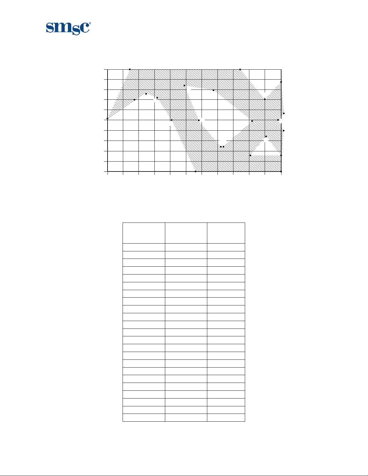
10/100 Non-PCI Ethernet Single Chip MAC + PHY
directly to the TP output pins without any external filters. During the idle period, no output signal is
transmitted on the TP outputs (except link pulse).
1.0
0.8
0.6
0.4
0.2
)
0.0
V
(
e
g
-0.2
a
t
l
o
-0.4
V
-0.6
-0.8
-1.0
0 102030405060708090100110
B
H
D
C
A
E
F
G
I
M
L
N
P
O
Q
J
K
W
R
S
U
V
T
TIME (ns)
FIGURE 9 - TP OUTPUT VOLTAGE TEMPLATE-10 MBPS
REFERENCE
TIME (NS)
INTERNAL
MAU
VOLTAGE
(V)
A 0 0
B 15 1.0
C 15 0.4
D 25 0.55
E 32 0.45
F 39 0
G 57 -1.0
H 48 0.7
I 67 0.6
J 89 0
K 74 -0.55
L 73 -0.55
M 61 0
N 85 1.0
O 100 0.4
P 110 0.75
Q 111 0.15
R 111 0
S 111 -0.15
T 110 -1.0
U 100 -0.3
V 110 -0.7
W 90 -0.7
Rev. 09/17/2002 Page 30 SMSC DS – LAN91C111 Rev. B
PRELIMINARY
 Loading...