

Page 1
Description:
MODEL.
Brand Name:
JOB NO.
Engineering Dept:
Artwork By: Date:
Checked By: Date:
Approved By: Date:
SERVICE MANUAL
8M28A CHASSIS
Design and specifications are subject to change without prior notice. (Only Referrence)
SIZE:A5
SERVICE MANUAL 8M28A
SKYWORTH
2012-4-28
Page 2
Content--------------------------------------------------------------2
11-17
18
19-20
21-29
30-47
48-51
52-59
Page 3
LED 8M26A
Page 4
TOSHIBA CODE
Component
PAL SECAM / BG DK PAL / I
NTSC / M
VHF LOW K1~S6
VHF HIGH S7~S36
VHF S37~DS57
44.25MHz ~ 140.25MHz
147.25MHz ~ 423.25MHz
431.25MHz ~ 863.25MHz
Asia\Europe
Page 5
40
55
80
For 22” LED
For 24” LED
For 32” LED
Page 6
(24 inches is 4 ohm)
(24 inches is 3W)
Page 7

80
(26inches is 8 ohm)
40
40
3
2
1
4.2
50
0.5
12000
40
3
Page 8
Standard
Standard
20
40
NO
YES
8
6
46
46
NO
Spanish
Page 9
4
2
4
0 40 7 0
0 40 7 0
0 40
40 85
-Y 0 5 0
30000
Page 10
Page 11
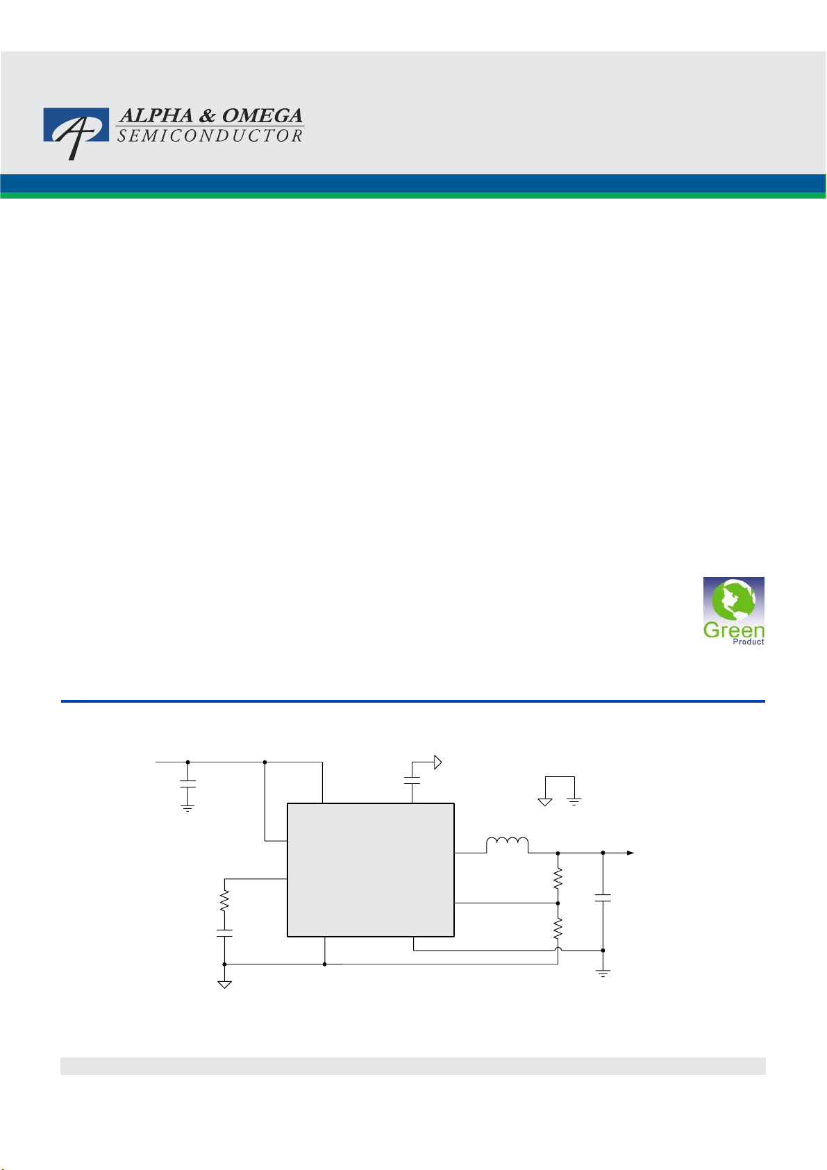
ʳ
Typical Application Circuit ʳ
AP1117
1A LOW DROPOUT POSITIVE ADJUSTABLE OR
FIXED-MODE REGULATOR
5V
C1
10uF
V
in
V
out
GND
Tab is V
out
( 5V/3.3V fixed output ) ʳ
ʳ
Connection Diagramʳ
ʳ
ʳ
3 PIN SOT223 3 PIN TO252 / TO263
C2
22uF
3.3V/1A
5V
Tab is V
V
out
V
out
Adj
C1
10uF
in
( 5V/2.5V ADJ output ) ʳ
Note:
(1VV
REFo
R1
121
R2
121
R
R
V
o
2.5V/1A
C2
ȍ
22uF
ȍ
2
)
1
(
Top View )
3
2
1
Tab is V
out
3 PIN SOT89
3
2
1
Tab is V
out
V
in
V
out
Adj ( GND)
V
in
V
out
Adj ( GND)
(
Top View )
3
2
1
Tab is V
out
3 PIN TO220
3
2
1
Tab is V
out
V
V
out
Adj ( GND)
in
V
in
V
out
Adj ( GND)
ʳ
ʳ
AP1117 Rev. 3 2 of 11 SEPTEMBER 2006
www.diodes.com © Diodes Incorporated
Page 12
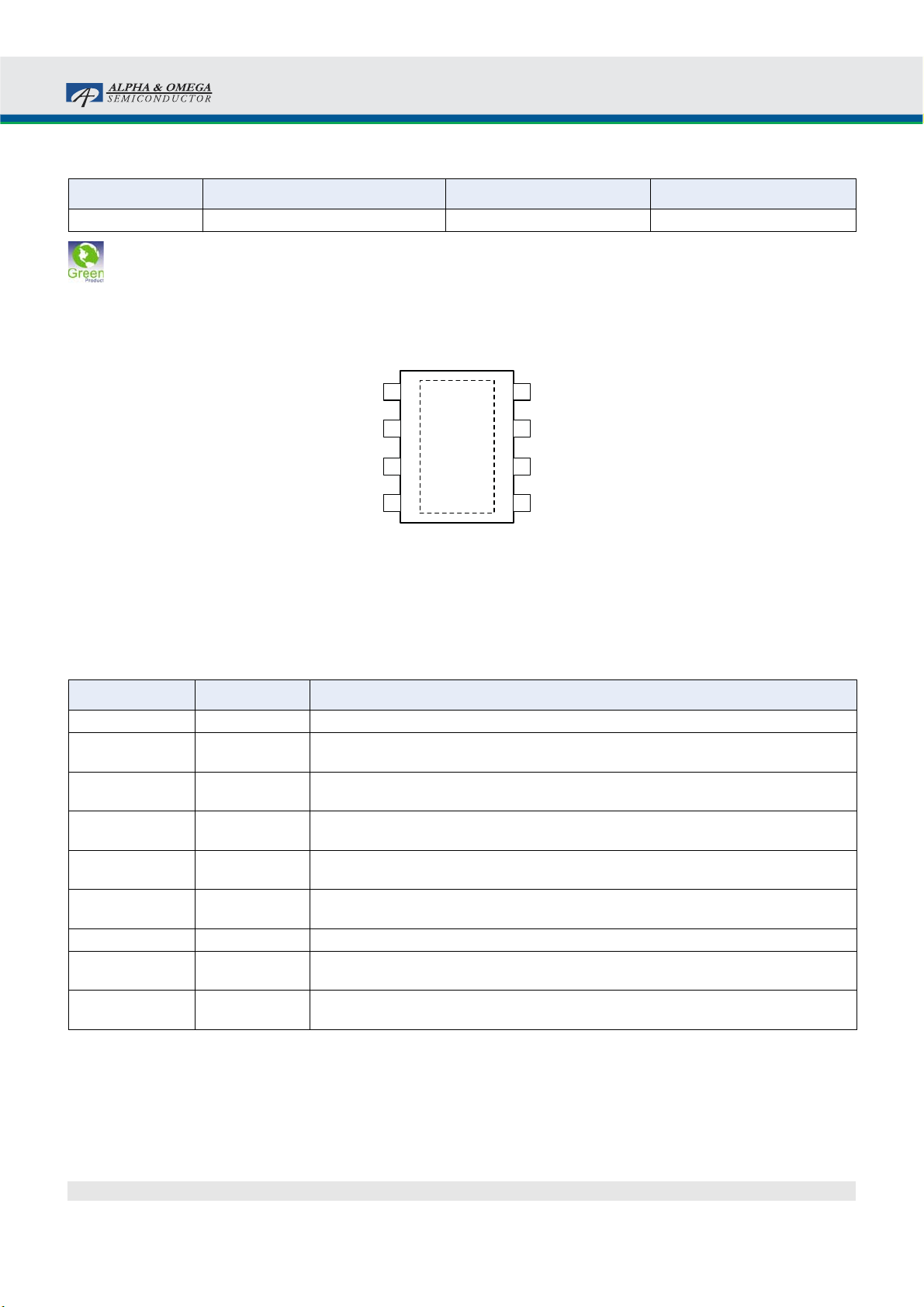
ʳ
Block Diagramʳ
AP1117
1A LOW DROPOUT POSITIVE ADJUSTABLE OR
FIXED-MODE REGULATOR
3
V
in
Thermal
Shutdown
Pin Descriptionsʳ
2
V
out
+
+
-
1.25V
CURRENT
LIMIT
+
-
+
1
GND
(FIXED)
1
Adj
NAME I/O PIN # FUNCTION
Adj (GND) I 1
V
out
V
in
O 2
I 3
A resistor divider from this pin to the V
(Ground only for Fixed-Mode).
The output of the regulator. A minimum of 10uF capacitor (0.15ȍ ESR 20ȍ)
must be connected from this pin to ground to insure stability.
The input pin of regulator. Typically a large storage capacitor (0.15ȍ ESR 20ȍ)
is connected from this pin to ground to insure that the input voltage does not sag
below the minimum dropout voltage during the load transient response. This pin
must always be 1.3V higher than V
pin and ground sets the output voltage
out
in order for the device to regulate properly.
out
ʳ
AP1117 Rev. 3 3 of 11 SEPTEMBER 2006
www.diodes.com © Diodes Incorporated
Page 13
A1semi 1A Fixed and Adjustable Low
A1
A1
A1
Electronics Ltd Dropout Linear Regulator(LDO)
Pin Configurations
L Package
(SOT-223)
V
OUT
T Package
(TO-220) (TO-252)
AS1117
U Package
(SOT-89)
3
INPUT
2
OUTPUT
1
ADJ/GND
V
OUT
3
2
1
R Package
INPUT
OUTPUT
ADJ/GND
3
INPUT
V
OUT
S Package
(TO-263)
V
OUT
3
2
1
3
2
1
INPUT
OUTPUT
ADJ/GND
INPUT
OUTPUT
ADJ/GND
Figure 2. Pin Configurations of AS1117
V
OUT
2
1
OUTPUT
ADJ/GND
AI SEMI ELECTRONICS LTD. 2
http://www.a1semi.com
Page 14
A1semi 1A Fixed and Adjustable Low
A1
A1
A1
Functional Block Diagram
Electronics Ltd Dropout Linear Regulator(LDO)
Thermal
Shutdown
AS1117
INPUT
Out
+
-
OUTPUT
GND (Fixed Output)
Figure 3. Functional Block Diagram of AS111 7
ADJ (Adjustable Output)
A1 SEMI ELECTRONICS LTD. 3
http://www.a1semi.com
Page 15
AOZ1051PI
EZBuck™ 3 A Synchronous Buck Regulator
General Description
The AOZ1051PI is a high efficiency, easy to use, 3 A
synchronous buck regulator. The AOZ1051PI works from
4.5 V to 18 V input voltage range, and provides up to 3 A
of continuous output current with an output voltage
adjustable down to 0.8 V.
The AOZ1051PI comes in an exposed pad SO-8
package and is rated over a -40 °C to +85 °C operating
ambient temperature range.
Features
z 4.5 V to 18 V operating input voltage range
z Synchronous Buck: 70 m internal high-side switch
and 40 m internal low-side switch (at 12 V)
z Up to 95 % efficiency
z External soft start
z Output voltage adjustable to 0.8 V
z 3 A continuous output current
z 500 kHz PWM operation
z Cycle-by-cycle current limit
z Pre-bias start-up
z Short-circuit protection
z Thermal shutdown
z Exposed pad SO-8 package
Applications
z Point of load DC/DC converters
z LCD TV
z Set top boxes
z DVD and Blu-ray players/recorders
z Cable modems
Typical Application
VIN
C1
10μF
VIN
EN
AOZ1051PI
COMP
R
C
C
C
Figure 1. 3.3 V 3 A Synchronous Buck Regulator, Fs = 500 kHz
Rev. 1.0 June 2011 www.aosmd.com Page 1 of 14
AGND
SS
PGND
C
SS
L1 4.7μH
LX
R1
FB
R2
VOUT
C2, C3
22μF
Page 16
AOZ1051PI
A
Ordering Information
Part Number Ambient Temperature Range Package Environmental
AOZ1051PI -40 °C to +85 °C EPAD SO-8 Green Product
AOS Green Products use reduced levels of Halogens, and are also RoHS compliant.
Please visit www.aosmd.com/web/quality/rohs_compliant.jsp for additional information.
Pin Configuration
PGND
VIN
GND
FB
1
2
3
4
PAD
(LX)
8
NC
7
SS
6
EN
5
COMP
Exposed Pad SO-8
(Top View)
Pin Description
Pin Number Pin Name Pin Function
1 PGND Power ground. PGND needs to be electrically connected to AGND.
2 VIN Supply voltage input. When VIN rises above the UVLO threshold and EN is logic high,
the device starts up.
3 AGND Analog ground. AGND is the reference point for controller section. AGND needs to be
electrically connected to PGND.
4 FB Feedback input. The FB pin is used to set the output voltage via a resistive voltage divider
between the output and AGND.
5 COMP External loop compensation pin. Connect a RC network between COMP and AGND to
compensate the control loop.
6 EN Enable pin. Pull EN to logic high to enable the device. Pull EN to logic low to disable the
device. If on/off control in not needed, connect EN to VIN and do not leave it open.
7 SS Soft-start pin. 5 μA current charging current.
8 NC No Connect Pin. Pin 8 is not internally connected. Connect this pin externally to LX and
use it for better thermal performance.
Exposed pad LX Switching node. LX is the drain of the internal PFET. LX is used as the thermal pad of the
power stage.
Rev. 1.0 June 2011 www.aosmd.com Page 2 of 14
Page 17
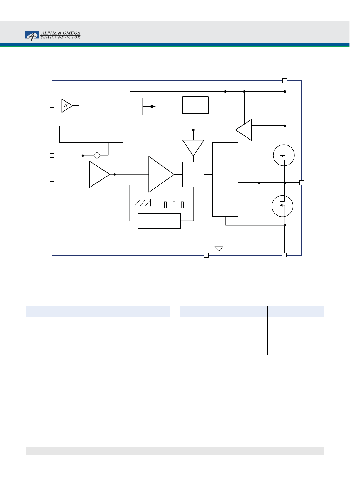
Block Diagram
AOZ1051PI
VIN
EN
SS
FB
COMP
Reference
& Bias
0.8V
UVLO
& POR
+
EAmp
–
Softstart
5μA
SS
5V LDO
Regulator
Internal
+5V
+
PWM
–
Comp
+
500kHz
Oscillator
OTP
ILimit
PWM
Control
Logic
Level
Shifter
FET
Driver
AGND
+
ISen
–
Q1
+
LX
Q2
PGND
Absolute Maximum Ratings
Exceeding the Absolute Maximum Ratings may damage the
device.
Parameter Rating
Supply Voltage (VIN) 20 V
LX to AGND -0.7 V to V
LX to AGND (20 ns) -5 V to 22 V
EN to AGND -0.3 V to V
FB, SS, COMP to AGND -0.3 V to 6.0 V
PGND to AGND -0.3 V to +0.3 V
Junction Temperature (T
Storage Temperature (T
ESD Rating
Note:
1. Devices are inherently ESD sensitive, handling precautions are
required. Human body model rating: 1.5 k
Rev. 1.0 June 2011 www.aosmd.com Page 3 of 14
(1)
) +150 °C
J
) -65 °C to +150 °C
S
in series with 100 pF.
+0.3 V
IN
+0.3 V
IN
2.0 kV
Recommended Operating Conditions
The device is not guaranteed to operate beyond the Maximum
Recommended Operating Conditions.
Parameter Rating
Supply Voltage (VIN) 4.5 V to 18 V
Output Voltage Range 0.8 V to 0.85 • V
Ambient Temperature (TA) -40 °C to +85 °C
Package Thermal Resistance
Exposed Pad SO-8 (4
Note:
2. The value of
FR-4 board with 2 oz. Copper, in a still air environment with
T
= 25 °C. The value in any given application depends on the
A
user’s specific board design.
4
is measured with the device mounted on a 1-in
JA
JA
(2)
)
50 °C/W
IN
2
Page 18
SY8086
Package Code
Package Code
High Efficiency 1.4MHz, 1A
Synchronous Step Down Regulator
Preliminary Specification
General Description
The SY8086 is a high-efficiency 1.4MHz synchronous
step-down DC-DC regulator ICs capable of delivering
up to 1A output current. The SY8086 operates over a
wide input voltage range from 2.5V to 5.5V and
integrate main switch and synchronous switch with
very low R
Low output voltage ripple and s mall external indu ctor
and capacitor sizes are achieved with 1.4MHz
switching frequency. This along with small SOT-23
footprint prov ides small PCB area application.
to minimize the conduction loss.
DS(ON)
Ordering Information
SY8086
SY8086
Temperature Range: -40
ƶƶƶƶ(ƶƶ
ƶƶ)ƶƶƶƶ
ƶƶƶƶ(ƶƶ
ƶƶ)ƶƶƶƶ
ƶƶƶƶ
ƶƶƶƶ
Temperature Code
Temperature Code
Optional Spec Code
Optional Spec Code
e
C to 85eC
Ordering Number Package type Note
SY8086AAC SOT23-5 1A
Featur es
•
Low R
250m
2.5-5.5V input voltage range
•
•
1.4MHz switching frequency minimizes the
external components
•
Internal softstart limits the inrush current
•
RoHS Compliant and Halogen Free
•
Compact package: SOT23 5 pin
for inter n al switche s (t op/ b ottom):
DS(ON)
Ω
/200m
Ω
Applications
•
Portable Navigation Device
•
Smart phone
•
USB Dongle
•
Set Top Box
•
Media Player
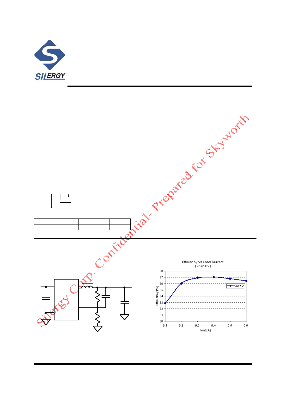
Typical Applications
V
IN
C
IN
EN
IN
LX
FB
GND
Figure 1. Schematic Diagram Figure2 Efficiency vs Load Current
SY8086 Rev. 0.11 Silergy Corp. Confidential- Prepared for Customer Use Only 1
L
R
R
C1(opt.)
1
2
V
OUT
C
OUT
Page 19

Pinout (top view)
SY8086
EN
EN
GND
GND
LX
LX
Top mark:
Pin Name Pin Number Pin Description
EN 1 Enable control. Pull high to turn on. Do not float.
GND 2 Ground pin
LX 3 Inductor pin. Connect this pin to the switching node of inductor
IN 4 Input pin. Decouple this pin to GND pin with at least 1uF ceramic cap
FB 5 Output Feedback Pin. Connect this pin to the center point of the outp ut
BE
xyz
(Device code: BE, x=year code, y= week code , z = lot number code )
resistor divider (as shown in Figure 1) to progra m th e output voltage:
Vout=0.6*(1+R
Absolute Maximu m Ratings
Supply Input Voltage --------------------------------------------------------------------------------------------- 6.0V
Enable, FB Voltage------------------------------------------------------------------------------------------------ V
Power Dissipation, P
Package Thermal Resistance (Note 2)
SOT23-5,
SOT23-5,
Junction Temperature Range ------------------------------------------------------------------------------------ 150°C
Lead Temperature (Soldering, 10 sec.) ------------------------------------------------------------------------- 260°C
Storage Temperature Range ------------------------------------------------------------------------------------ESD Susceptibility (Note 2)
HBM (Human Body Mode) -------------------------------------------------------------------------------------- 2kV
MM (Machine Mode) ----------------------------------------------------------------------------------------------200V
D
@ TA = 25°C SOT-23-5 -------------------------------------------------------------- 0.4W
θ
JA
------------------------------------------------------------------------------------------ 250°C/W
θ
JC
-------------------------------------------------------------------------------------------130°C/W
1
1
2
2
3
3
SOT23-5
1/R2
(Note 1)
5
5
FB
FB
4
4
IN
IN
)
IN
+ 0.6V
-
65°C to 150°C
Recommended Operating Conditions
Supply Input Voltage -------------------------------------------------------------------------------------------- 2.5V to 5.5V
Junction Temperature Range ---------------------------------------------------------------------------------- -40°C to 125°C
Ambient Temperature Range ----------------------------------------------------------------------------------
(Note 3)
-
40°C to 85°C
SY8086 Rev. 0.11 Silergy Corp. Confidential- Prepared for Customer Use Only 2
Page 20

IC Block Diagram
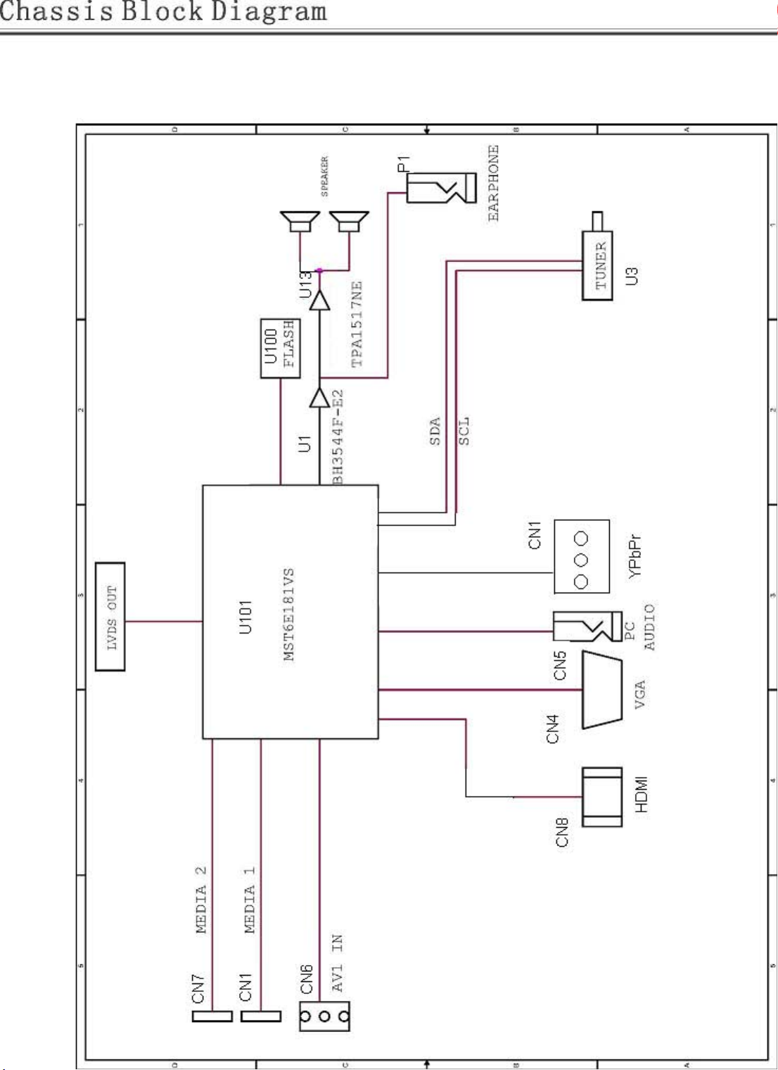
U10(LCDTV CONTROLLER WITH VIDEO ECODE)MST6E181VS
PIN DIAGRAM (MST6E181VS)
162
161
160
159
158
157
156
155
154
153
152
151
150
149
148
147
146
145
144
143
142
141
140
139
138
137
136
135
134
133
132
131
130
129
NC
NC
LDQS0
LDQM0
A_DDR1_BA0
DVDD_DDR_1.2V
A_DDR1_DQ8
A_DDR1_DQ9
AVDDIO_2.5V
A_DDR1_DQ10
A_DDR1_DQ11
A_DDR1_DQ12
A_DDR1_DQ13
A_DDR1_DQ14
AVDDIO_2.5V
A_DDR1_DQ15
A_DDR1_MCLKZ
AVDDIO_2.5V
A_DDR1_MCLK
A_DDR1_CKE
A_DDR1_A12
A_DDR1_A11
A_DDR1_A9
AVDDIO_2.5V
A_DDR1_A8
A_DDR1_A7
A_DDR1_A6
A_DDR1_A5
A_DDR1_A4
AVDD_NODIE
DVDD_NODIE
GND_EFUSE
GPIO11/SAR0
GPIO12/SAR1
GPIO13/SAR2
GPIO10/PMGPIO
GPIO6/PM1/TX
GPIO8/PM5/RX
GPIO9/PM6/CS1
AVDDIO_2.5V
GPIO7/PM4/POWER_ON
163
164
165
166
167
168
169
170
171
172
173
174
175
176
177
178
179
180
181
182
183
184
185
186
187
188
189
190
191
192
193
194
195
196
197
198
199
200
201
202
203
204
205
206
207
208
209
210
211
212
213
214
215
216
217
AVDD_PLL
UDQM0
UDQS0
A_MVREF
NC
VDDC
DDCR_DA
VDDP_3
DDCR_CK
TESTPIN
DM_P0
DP_P0
DM_P1
DP_P1
SPI_CK
SPI_DI
SPI_DO
SPI_CZ
DDCA_CK
DDCA_DA
E-pad
AVDDIO_2.5V
A_DDR1_DQ4
A_DDR1_DQ7
A_DDR1_DQ6
A_DDR1_DQ5
AVDDIO_2.5V
A_DDR1_DQ3
A_DDR1_DQ2
A_DDR1_DQ1
A_DDR1_DQ0
AVDDIO_2.5V
A_DDR1_CAS
A_DDR1_RAS
A_DDR1_WEZ
A_DDR1_BA1
A_DDR1_A0
A_DDR1_A1
A_DDR1_A2
A_DDR1_A3
A_DDR1_A10
NC
NC
VDDC
VDDP_2
GPIO21/PWM1
GPIO20/PWM0
GPIO77/I2S_OUT_MUTE/PWM3/LVSYNC
MST6E181VS
128
127
126
125
124
123
122
121
120
119
118
117
116
115
VDDC
AVDD_LPLL
R_ODD7/RXO0-
R_ODD5/RXO1-
AVDD2P5_MOD
GPIO75/I2S_IN_SD/PWM5/TX3/LDE
GPIO74/I2S_IN_WS/PWM4/RX3/LCK
GPIO76/I2S_IN_BCK/PWM2/LHSYNC
R_ODD3/RXO2-
R_ODD1/RXOC-
R_ODD6/RXO0+
R_ODD4/RXO1+
R_ODD2/RXO2+
114
113
112
111
110
G_ODD3/RXE0-
G_ODD7/RXO3-
G_ODD5/RXO4-
G_ODD6/RXO3+
G_ODD4/RXO4+
R_ODD0/RXOC+
109
G_ODD2/RXE0+
AVDD2P5_MOD
108
G_ODD1/RXE1-
107
G_ODD0/RXE1+
106
B_ODD7/RXE2-
105
B_ODD6/RXE2+
104
B_ODD5/RXEC-
103
B_ODD4/RXEC+
102
B_ODD3/RXE3-
101
B_ODD2/RXE3+
100
B_ODD1/RXE4-
99
B_ODD0/RXE4+
98
NC
97
GPIO49
96
GPIO47
95
GPIO45
94
GPIO38
93
GPIO37
92
GPIO36
91
GPIO32/I2S_OUT_BCK
90
GPIO30/I2S_OUT_MCK
89
GPIO28
88
VDDP_1
87
VDDC
86
GPIO27/SPDIF_OUT
85
GPIO26/SPDIF_IN/RX1/PWM3
84
GPIO25/TUNER_SDA
83
GPIO24/TUNER_SCL
82
GPIO23/I2S_OUT_SD/TX2
81
GPIO22/I2S_OUT_WS/RX2
80
TAGC
79
SIFM
78
SIFP
77
AVDD25_PGA
76
VIFP
75
VIFM
74
AVSS_PGA
73
AVDD25_REF
72
AVDD_DMPLL
71
XTAL_OUT
70
XTAL_IN
69
NC
68
NC
67
NC
66
LINEOUT_R0
65
LINEOUT_L0
64
LINEOUT_R3
63
LINEOUT_L3
62
AVDD_AU33
61
LINEIN_R5
60
LINEIN_L5
59
LINEIN_R4
58
LINEIN_L4
57
LINEIN_R3
56
LINEIN_L3
55
U?
IRIN
2
1
9876543
10
RX1N
AVDD_DVI_3.3V
RX0P
RX0N
RXCP
RXCN
HOTPLUGA
RESET
CEC
HSYNC0
VDDC
NC
NC
SOGIN0
BIN0P
2726252423222120191817161514131211
GIN0M
GIN0P
VSYNC0
RIN0P
SOGIN1
BIN1P
AVDD2P5_ADC
AVDD1P2
GIN1M
GIN1P
CVBS2
CVBS3
CVBS4
AVDD3P3_ADC
RIN1P
CVBS0
CVBS1
4443424140393837363534333231302928
CVBS_OUT1
VCOM
45
LINEIN_L1
LINEIN_R0
LINEIN_L0
VRP
VRM
LINEIN_R1
AVDD_AU25
VAG
545352515049484746
NCNCNCNCNC
ARC
DDCDA_CK
RX2P
RX2N
DDCDA_DA
RX1P
-13-
Page 21

PDF "pdfFactory Pro" www.fineprint.cn
Page 22

PDF "pdfFactory Pro" www.fineprint.cn
Page 23

PDF "pdfFactory Pro" www.fineprint.cn
Page 24

PDF "pdfFactory Pro" www.fineprint.cn
Page 25

PDF "pdfFactory Pro" www.fineprint.cn
Page 26

PDF "pdfFactory Pro" www.fineprint.cn
Page 27

PDF "pdfFactory Pro" www.fineprint.cn
Page 28

MST6M181VG/MST6M182VG
2012010018
2012010018
LCD Television System-on-Chip
Preliminary Pin Diagram/Description and Mechanical Dimensions Version 0.2
Doc. No.:
PIN DIAGRAM (MST6M181VG/MST6M182VG)
1 2 3 4 5 6 7 8 9 1011121314 1516
A RXCKP RXCKN NC NC HWRESET GPIO7 GPIO6 GND USB1_DM USB0_DP USB0_DM A
B RX1N RX 0P RX0 N NC NC NC NC IRIN GPIO8 SAR0 PWM0 USB1_DP DDCR_CK SCZ SDO B
C RX2N RX2P RX1P NC NC NC NC GPIO9 SAR2 SA R1 PWM1 GND DDC R_DA SCK SDI C
D DDCD_CK ARC
ESOGIN0BIN0PHSYNC0
DDCD_DAHOTPLUG
A
NC CEC BYPA SS
MStar Confidential
F RIN0P GIN0M GIN0P VSYNC0 GND
G GND GN D GND
for Skyworth
H SOGIN1 BIN1P
J RIN1P GIN1M GIN1P AVDD_33
K CVBS2 CVBS1 NC
Internal Use Only
L CVBS0 VC OM AUVA G AUVRP
M CVBSOUT AUL0 AUL3 GND
AVDD_AL
IVE
AVDD_D
MPLL
AVDD_ME
MPLL
AVDD_MODAVDD_ RE
AVDD_M
OD
AVDD_AU
33
AVDD_126DVDD_D
AVDD_25
AVDD_AU
VDDC VDDC GND GND GND
25
VDDC VDDC GND GND GND MVREF
F
VDDP VDDC V DDC FLK2 GCLK6 RL V2P L
VDDP
AVDD_D
DR
DR
AVDD_D
DDCA_CK DDCA_D A GPIO10 GND LEDON HCO N DPM D
DR
GND GND GND
AVDD_ DDRAVDD_D
DR
AVDD_DDRSCAN_BL
GND SAR3 OPT_N GCLK4 G
K
SCAN_BL
K1
GSP/
VST
GSP_R/
GCLK1
VGH_OD
D
RLVCKM RLVCKP RLV2M M
GOE/
POL
GCLK2
WPWM OPT_P F
SOE FLK3 H
GSC/
GCLK 3
GCLK 5
FLK J
VGH_EVE
N
E
K
N AUR0 AUL1 AUR3 AUOUTL1
PAUR1 AUL2AUOUTR1 GND PGA_COM GND GND
RAUR2AUOUTL0 XOUT GND GND VIFM GND
T AUOUTR0 XIN TAGC GND VIFP GND
1 2 3 4 5 6 7 8 9 1011121314 1516
Doc. No.:
AVDD_PG
Copyright
GND NC NC RLV1M RLV1P RLV0M RLV0P RLV3M RLV3P N
A
I2S_OUT
I2S_OUT
I2S_OUT
2011 MStar Semiconductor, Inc. All rights reserved.
SPDIFI LLV5M LLV4M LLV3P LLV2M LLV1M RLV4M RLV4P P
_SD
I2S_OUT
_MCK
_BCK
SPDIFO LLV3M LLVCKM LLV0M L LV0P T
_WS
- 1 - 8/29/2011
PDF "pdfFactory Pro" www.fineprint.cn
LLV5P LLV4P LLVCKP LLV2P LLV1P RLV5M RLV5P R
Page 29

MST6M181VG/MST6M182VG
2012010018
2012010018
LCD Television System-on-Chip
Preliminary Pin Diagram/Description and Mechanical Dimensions Version 0.2
Doc. No.:
PIN DESCRIPTION
Analog Interface
Pin Name Pin Type Function Pin
HSYNC0 Schmitt Trigger Input
w/ 5V-tolerant
VSYNC0 Schmitt Trigger Input
w/ 5V-tolerant
BIN0P Analog Input Analog Blue Input from Channel 0 E3
SOGIN0 Analog Input Sync On Green Input from Channel 0 E2
GIN0P Analog Input Analog Green Input from Channel 0 F3
GIN0M Analog Input Reference Ground for Analog Green Input from Channel 0 F2
RIN0P Analog Input Analog Red Input from Channel 0 F1
MStar Confidential
BIN1P Analog Input Analog Blue Input from Channel 1 H3
SOGIN1 Analog Input Sync On Green Input from Channel 1 H2
GIN1P Analog Input Analog Green Input from Channel 1 J3
GIN1M Analog Input Reference Ground for Analog Green Input from Channel 1 J2
RIN1P Analog Input Analog Red Input from Channel 1 J1
HSYNC / Composite Sync for VGA Input from channel 0 E4
VSYNC for VGA Input from channel 0 F4
for Skyworth
Analog Video Input/Output Interface
Pin Name Pin Type Function Pin
CVBS2 Analog Input CVBS (Composite) Video Input Channel 2 K1
CVBS1 Analog Input CVBS (Composite) Video Input Channel 1 K2
Internal Use Only
CVBS0 Analog Input CVBS (Composite) Video Input Channel 0 L1
VCOM Analog Input CVBS Input Reference Ground L2
CVBSOUT Analog Output CVBS (Composite) Video Output Channel M1
Analog Audio Input/Output Interface
Pin Name Pin Type Function Pin
I2S_OUT_WS I/O w/ 5V-tolerant Word Select Output; 4mA driving strength /
Universal Asynchronous Receiver 2 (UART2_RX)
I2S_OUT_SD I/O w/ 5V-tolerant Audio Serial Data Output; 4mA driving strength /
Universal Asynchronous Transmitter 2 (UART2_TX)
SPDIFI Input w/ 5V-tolerant S/PDIF Audio Input /
Pulse Width Modulation Output; 4mA driving strength
(PWM3)
SPDIFO Output S/PDIF Audio Output; 4mA driving strength T9
Doc. No.:
Copyright
2011 MStar Semiconductor, Inc. All rights reserved.
- 2 - 8/29/2011
T8
P8
P9
PDF "pdfFactory Pro" www.fineprint.cn
Page 30

MST6M181VG/MST6M182VG
2012010018
2012010018
LCD Television System-on-Chip
Preliminary Pin Diagram/Description and Mechanical Dimensions Version 0.2
Doc. No.:
Pin Name Pin Type Function Pin
I2S_OUT_MCK Output w/ 5V-tolerant Audio Master Clock Output R8
I2S_OUT_BCK Output w/ 5V-tolerant Audio Bit Clock Output R9
AUL0 Analog Input Audio Line Input Left Channel 0 M2
AUR0 Analog Input Audio Line Input Right Channel 0 N1
AUL1 Analog Input Audio Line Input Left Channel 1 N2
AUR1 Analog Input Audio Line Input Right Channel 1 P1
AUL2 Analog Input Audio Line Input Left Channel 2 P2
AUR2 Analog Input Audio Line Input Right Channel 2 R1
AUL3 Analog Input Audio Line Input Left Channel 3 M3
AUR3 Analog Input Audio Line Input Right Channel 3 N3
AUVRP Analog Output Positive Reference Voltage for Audio ADC L4
MStar Confidential
AUVAG Analog Output Reference Voltage for Audio Common Mode L3
AUOUTL1 Analog Output Main Audio Output Left Channel 1 N4
AUOUTR1 Analog Output Main Audio Output Right Channel 1 P3
AUOUTL0 Analog Output Main Audio Output Left Channel 0 R2
AUOUTR0 Analog Output Main Audio Output Right Channel 0 T2
for Skyworth
Mini-LVDS Interface
Pin Name Pin Type Function Pin
LLV5M Output Mini-LVDS L-Link Channel 5 Negative Data Output P10
LLV5P Output Mini-LVDS L-Link Channel 5 Positive Data Output R10
Internal Use Only
LLV4M Output Mini-LVDS L-Link Channel 4 Negative Data Output P11
LLV4P Output Mini-LVDS L-Link Channel 4 Positive Data Output R11
LLV3M Output Mini-LVDS L-Link Channel 3 Negative Data Output T11
LLV3P Output Mini-LVDS L-Link Channel 3 Positive Data Output P12
LLV2M Output Mini-LVDS L-Link Channel 2 Negative Data Output P13
LLV2P Output Mini-LVDS L-Link Channel 2 Positive Data Output R13
LLV1M Output Mini-LVDS L-Link Channel 1 Negative Data Output P14
LLV1P Output Mini-LVDS L-Link Channel 1 Positive Data Output R14
LLV0M Output Mini-LVDS L-Link Channel 0 Negative Data Output T14
LLV0P Output Mini-LVDS L-Link Channel 0 Positive Data Output T15
LLVCKM Output Mini-LVDS L-Link Negative Clock Output T12
LLVCKP Output Mini-LVDS L-Link Positive Clock Output R12
RLV5M Output Mini-LVDS R-Link Channel 5 Negative Data Output R15
RLV5P Output Mini-LVDS R-Link Channel 5 Positive Data Output R16
Doc. No.:
Copyright
PDF "pdfFactory Pro" www.fineprint.cn
2011 MStar Semiconductor, Inc. All rights reserved.
- 3 - 8/29/2011
Page 31

MST6M181VG/MST6M182VG
2012010018
2012010018
LCD Television System-on-Chip
Preliminary Pin Diagram/Description and Mechanical Dimensions Version 0.2
Doc. No.:
Pin Name Pin Type Function Pin
RLV4M Output Mini-LVDS R-Link Channel 4 Negative Data Output P15
RLV4P Output Mini-LVDS R-Link Channel 4 Positive Data Output P16
RLV3M Output Mini-LVDS R-Link Channel 3 Negative Data Output N14
RLV3P Output Mini-LVDS R-Link Channel 3 Positive Data Output N15
RLV2M Output Mini-LVDS R-Link Channel 2 Negative Data Output M16
RLV2P Output Mini-LVDS R-Link Channel 2 Positive Data Output L16
RLV1M Output Mini-LVDS R-Link Channel 1 Negative Data Output N10
RLV1P Output Mini-LVDS R-Link Channel 1 Positive Data Output N11
RLV0M Output Mini-LVDS R-Link Channel 0 Negative Data Output N12
RLV0P Output Mini-LVDS R-Link Channel 0 Positive Data Output N13
RLVCKM Output Mini-LVDS R-Link Negative Clock Output M14
MStar Confidential
RLVCKP Output Mini-LVDS R-Link Positive Clock Output M15
TCON Interface
Pin Name Pin Type Function Pin
POL Output Polarity Control Single E15
SOE Output Source Output Enable H15
GSP/
VST
GCLK6 Output Gate Clock for GIP Panel L15
GCLK5 Output Gate Clock for GIP Panel K15
Internal Use Only
GCLK4 Output Gate Clock for GIP Panel G16
GSC/
GCLK3
GOE/
GCLK2
GSP_R/
GCLK1
SCAN_BLK1 Output Scan Backlight Control Signal 1 F14
SCAN_BLK Output Scan Backlight Control Signal E14
OPT_N Output The Output Pin to Indicate Reverse State G15
for Skyworth
Output Gate Start Pulse for LTD Panel /
Vertical start pulse for GIP Panel
Output Gate Shift Clock for LTD Panel /
Gate Clock for GIP Panel
Output Gate Clock for GIP Panel /
Gate Output Enable for LTD Panel
Output Right Gate Start Pulse for LTD Panel /
Gate Clock for GIP Panel
H14
J15
E16
J14
OPT_P Output The Output Pin to Indicate Reverse State F16
FLK3 Output Gate Modulation Signal H16
FLK2 Output Gate Modulation Signal L14
FLK Output Gate Modulation Signal J16
Doc. No.:
Copyright
2011 MStar Semiconductor, Inc. All rights reserved.
- 4 - 8/29/2011
PDF "pdfFactory Pro" www.fineprint.cn
Page 32

MST6M181VG/MST6M182VG
2012010018
2012010018
LCD Television System-on-Chip
Preliminary Pin Diagram/Description and Mechanical Dimensions Version 0.2
Doc. No.:
Pin Name Pin Type Function Pin
WPWM Output PWM Output for Wavy Noise F15
HCON Output H Inversion Control Signal on DPC D15
DPM Output Power Sequence Control Signal D16
LEDON Output LED On D14
VGH_ODD Output VGH Odd for GIP Panel K14
VGH_EVEN Output VGH Even for GIP Pane K16
DVI/HDMI Interface
Pin Name Pin Type Function Pin
RXCKN DVI/HDMI Input Negative DVI/HDMI Input for A Link Clock Channel A3
RXCKP DVI/HDMI Input Positive DVI/HDMI Input for A Link Clock Channel A2
MStar Confidential
RX0N DVI/HDMI Input Negative DVI/HDMI Input for A Link Data Channel 0 B3
RX0P DVI/HDMI Input Positive DVI/HDMI Input for A Link Data Channel 0 B2
RX1N DVI/HDMI Input Negative DVI/HDMI Input for A Link Data Channel 1 B1
RX1P DVI/HDMI Input Positive DVI/HDMI Input for A Link Data Channel 1 C3
RX2N DVI/HDMI Input Negative DVI/HDMI Input for A Link Data Channel 2 C1
RX2P DVI/HDMI Input Positive DVI/HDMI Input for A Link Data Channel 2 C2
ARC DVI/HDMI Output Audio Return Channel D2
for Skyworth
Serial Flash Interface
Internal Use Only
Pin Name Pin Type Function Pin
SCK
SDI
SDO Input w/ 5V-tolerant SPI Flash Serial Data Output B16
SCZ
IRIN Input w/ 5V-tolerant IR Receiver Input B9
Output
Output
Output
SPI Flash Serial Clock C15
SPI Flash Serial Data Input C16
SPI Flash Chip Select B15
GPIO Interface
Pin Name Pin Type Function Pin
GPIO10 I/O w/ 5V-tolerant
GPIO9 I/O w/ 5V-tolerant General Purpose Input/Output; 4mA driving strength C9
GPIO8 I/O w/ 5V-tolerant General Purpose Input/Output /
GPIO7 I/O w/ 5V-tolerant General Purpose Input/Output; 4mA driving strength
Doc. No.:
Copyright
General Purpose Input/Output; 4mA driving strength
Universal Asynchronous Receiver 0 (UART0_RX)
For Power Management Only
- 5 - 8/29/2011
2011 MStar Semiconductor, Inc. All rights reserved.
PDF "pdfFactory Pro" www.fineprint.cn
D12
B10
A10
Page 33

MST6M181VG/MST6M182VG
2012010018
2012010018
LCD Television System-on-Chip
Preliminary Pin Diagram/Description and Mechanical Dimensions Version 0.2
Doc. No.:
Pin Name Pin Type Function Pin
GPIO6 I/O w/ 5V-tolerant General Purpose Input/Output /
Word Select Output; 4mA driving strength (I2S_OUT_WS) /
Universal Asynchronous Transmitter 0 (UART0_TX)
PWM1 Output w/ 5V-tolerant Pulse Width Modulation Output; 4mA driving strength C12
PWM0 Output w/ 5V-tolerant Pulse Width Modulation Output; 4mA driving strength B12
SAR3 Analog Input SAR Low Speed ADC Input 3 G14
SAR2 Analog Input SAR Low Speed ADC Input 2 C10
SAR1 Analog Input SAR Low Speed ADC Input 1 C11
SAR0 Analog Input SAR Low Speed ADC Input 0 B11
A11
USB Interface
MStar Confidential
Pin Name Pin Type Function Pin
USB0_DP Analog I/O USB Non Inverting Data Input/Output for Port 0 A14
USB0_DM Analog I/O USB Inverting Data Input/Output for Port 0 A15
USB1_DP Analog I/O USB Non Inverting Data Input/Output for Port 1 B13
USB1_DM Analog I/O USB Inverting Data Input/Output for Port 1 A13
for Skyworth
VIF Interface
Pin Name Pin Type Function Pin
VIFM Analog Input Negative Video IF Input R6
VIFP Analog Input Positive Video IF Input T6
Internal Use Only
TAGC Analog Output Tuner Automatic Gain Control Output T4
PGA_COM Analog Input VIF PGA Negative Source P5
Misc. Interface
Pin Name Pin Type Function Pin
HWRESET Schmitt Trigger Input
w/ 5V-tolerant
DDCD_DA I/O w/ 5V-tolerant HDCP Serial Bus Data / DDC Data of DVI/HDMI D3
DDCD_CK Input w/ 5V-tolerant HDCP Serial Bus Clock / DDC Clock of DVI/HDMI D1
DDCR_DA I/O w/ 5V-tolerant DDC Data for ROM C14
DDCR_CK Input w/ 5V-tolerant DDC Clock for ROM B14
HOTPLUGA I/O w/ 5V-tolerant Hot-plug control for DVI/HDMI D4
DDCA_DA I/O w/ 5V-tolerant DDC Data for Analog port D11
Hardware Reset; active high A9
DDCA_CK I/O w/ 5V-tolerant DDC Clock for Analog port D10
Doc. No.:
Copyright
PDF "pdfFactory Pro" www.fineprint.cn
2011 MStar Semiconductor, Inc. All rights reserved.
- 6 - 8/29/2011
Page 34

MST6M181VG/MST6M182VG
2012010018
2012010018
LCD Television System-on-Chip
Preliminary Pin Diagram/Description and Mechanical Dimensions Version 0.2
Doc. No.:
Pin Name Pin Type Function Pin
XIN Crystal Oscillator Input Crystal Oscillator Input T3
XOUT Crystal Oscillator
Output
BYPASS For External Bypass Capacitor D7
CEC I/O Consumer Electronics Control D6
MVREF Input Reference Voltage for DDR SDRAM Interface K13
Crystal Oscillator Output R3
Power Pins
Pin Name Pin Type Function Pin
AVDD_33 3.3V Power Analog 3.3V Power J4
AVDD_25 2.5V Power Analog 2.5V Power H6
MStar Confidential
AVDD_126 1.26V Power Analog 1.26V Power H7
AVDD_AU25 2.5V Power Audio 2.5V Power J6
AVDD_AU33 3.3V Power Audio 3.3V Power M5
AVDD_DMPLL 3.3V Power Crystal Power K4
AVDD_REF 2.5V Power Demod ADC Power K6
AVDD_PGA 2.5V Power Demod PGA Power N5
AVDD_MOD 3.3V Power MOD Power K5, L5
AVDD_MEMPLL 3.3V Power PLL Power J5
AVDD_DDR 1.8V Power DDR Power D9, E13, G8, M10, M11
for Skyworth
DVDD_DDR 1.26V Power DDR 1.26V Power H8
Internal Use Only
AVDD_ALIVE 3.3V Power Alive Domain IO Power H4
VDDC 1.26V Power Digital Core Power J7, J8, K7, K8, L7, L8
VDDP 3.3V Power Digital Input/Output Power L6, M6
GND Ground Ground A12, C13, D13, F13, G1-G3, G13,
H9-H11, J9-J11, K9-K11, M4, N6, P4,
P6, P7, R4, R5, R7, T5, T7
No Connects
Pin Name Pin Type Function Pin
NC No connect A5, A6, B4-B7, C4-C7, D5, K3, N8, N9
Doc. No.:
Copyright
2011 MStar Semiconductor, Inc. All rights reserved.
- 7 - 8/29/2011
PDF "pdfFactory Pro" www.fineprint.cn
Page 35

MST6M181VG/MST6M182VG
prop
malfunctio
performance degradation.
2012010018
2012010018
LCD Television System-on-Chip
Preliminary Pin Diagram/Description and Mechanical Dimensions Version 0.2
Doc. No.:
DISCLAIMER
MSTAR SEMICONDUCTOR RESERVES THE RIGHT TO MAKE CHANGES WITHOUT FURTHER NOTICE
TO ANY PRODUCTS HEREIN TO IMPROVE RELIABILITY, FUNCTION OR DESIGN. NO
RESPONSIBILITY IS ASSUMED BY MSTAR SEMICONDUCTOR ARISING OUT OF THE APPLICATION
OR USER OF ANY PRODUCT OR CIRCUIT DESCRIBED HEREIN; NEITHER DOES IT CONVEY ANY
LICENSE UNDER ITS PATENT RIGHTS, NOR THE RIGHTS OF OTHERS.
Electrostatic charges accumulate on both test equipment and human bodyand can dischargewithout
detection. MST6M181VG/MST6M182VG comes with ESD protection circuitry; however, the device
may be permanently damaged when subjected to high energy discharges. The device should be
handled with
er ESDprecautions toprevent
nand
REVISION HISTORY
Document Description Date
MST6M181VG/MST6M182VG_pin_v01 Initial release Aug 2011
MST6M181VG/MST6M182VG_pin_v02 Added Ball Diameter to Mechanical Dimensions Aug 2011
MStar Confidential
for Skyworth
Internal Use Only
Doc. No.:
Copyright
PDF "pdfFactory Pro" www.fineprint.cn
2011 MStar Semiconductor, Inc. All rights reserved.
- 8 - 8/29/2011
Page 36

Preliminary Pin Diagram/Description and Mechanical Dimensions Version 0.2
2012010018
2012010018
Doc. No.:
MECHANICAL DIMENSIONS
MST6M181VG/MST6M182VG
LCD Television System-on-Chip
D
E
M
S
MStar Confidential
A1
A
10
12
14
16
15
11
13
82
7
for Skyworth
Internal Use Only
E1
e
4
6
5
19
3
A
B
C
D
E
F
G
H
J
K
L
M
N
P
R
T
Symbol
A - - 1.40 - - 0.055
A1 0.27 - 0.37 0.011 - 0.015
M 0.70 REF 0.028 REF
S 0.22 0.26 0.30 0.009 0.010 0.012
D - 13.50 - - 0.531 -
E - 13.50 - - 0.531 -
D1 - 12.00 - - 0.472 -
E1 - 12.00 - - 0.472 -
e - 0.80 - - 0.031 -
Ball
Diameter
Millimeter Inch
Min. Nom. Max. Min. Nom. Max.
- 0.40 - - 0.016 -
b (200x)
- 9 - 8/29/2011
Doc. No.:
e
D1
Copyright
2011 MStar Semiconductor, Inc. All rights reserved.
PDF "pdfFactory Pro" www.fineprint.cn
Page 37

IC Block Diagram
8᧤0%,7&0266(5,$/)/$6+᧥623
Address
Generator
MemoryArray
P age B uffer
SI/SIO0
SO /SIO1
CS#,
WP#,
HOLD#
S CLK Clock G enerator
Data
Register
SRAM
B uffer
M ode
Logic
S tate
Machine
Y-D ecoder
Sense
Am plifier
HV
Generator
Output
B uffer
-15-
Page 38

Page 39

8M28A/S Factory Adjust Menu
(V0.0)
1. Description
Enter factory mode:
Open source menu,and then press digital butto n “ 3”, “1”, “9” , “5” in
turns to enter the factory menu. Press ↑ and ↓ button to choose the
item, press OK button enter the submenu, press MENU to ruturn to
upper menu , press ← and → button t o adj ust the va lu e,
Leave fact ory mode:
Press menu button to back to upper menu until leave factory mode。
Software in formation:
Enter factory mode, you can get the software information from the
bottom of the menu.
Panel inform ati on :
Enter factory mode, enter “Panel SETTING” item, you can get the
panel information fro m the bottom of this menu.
Aging mode:
You can press the shortcut key in the factory remote control to open
or close the aging mode.
ADC adjusts:
YPBPR source ADC:
Switch to YPBPR source, input 100% color bar pattern, enter
Page 40

factory, select “AUTO ADC” item in the “ADC CALIBRATION”
menu, press → button to begin auto adjust. When it is finish, it will
show “OK” or “FAILE”. If “FAILE” is showed, you need to try
again.
NOTE: YPBPR ADC need to do twice by use 576P and 720P
signal separate.
VGA source ADC:
Switch to PC source, input tessellated white and black signal,
enter factory, select “AUTO ADC” item in the “ADC CALIBRATION”
menu, press → button to begin auto adjust. When it is finish, it will
show “OK” or “FAILE”. If “FAILE” is showed, you nee d to try again.
Page 41

White balance:
Enter factory mode, enter “W/B ADJUST” item, you can adjust white
balance in this menu.
Over scanning:
Enter factory mode, enter “Panel SETTING” submenu, enter
“OVERSCAN” submenu, you can a dj ust th e ove r sca n in these menu.
OutFactory re set:
Enter factory mode, enter “SYSTEM SETTING” item, select “OUT
FACTORY SET” item and press OK button to reset the flash memory.
TV set will rest art when it is finish.
INIT EEPROM:
Enter factory mode, enter “SYSTEM SETTING” item, select “FAC
RESET DEFAULT” item and press OK button to reset the EEPROM.
TV set will rest art when it is finish.
Page 42

Update software (by USB):
Copy the new software (name by “MERGE.bin”) to the root directory
of USB drive. Plug the drive to the USB2 socket (if there are two USB
socket, make sure you use the socket 2). Enter factory, select “Software
Update (USB)” item and press OK button to begin update. TV set will
restart when finish. Note, you need to restart the TV set again by AC
power.
We suggest you need to do “INIT EEPROM” and “Factory reset”
after software upda t
Page 43

2. More information
FACTORY MENU Default Value Remark
ADC ADJUST
MODE Select source
R-GAIN Red gain
G-GAIN Green gain
B-GAIN Blue gain
R-OFFSET Red offset
G-OFFSET Green offs et
B-OFFSET Blue offs et
AUTO ADC Auto ADC calibration
W/B ADJUST
MODE Select source
TEMPERATURE Select Neutral/Warm/C ool/Personal
R-GAIN Red gain
G-GAIN Green gain
B-GAIN Blue gain
R-OFFSET Red offset
G-OFFSET Green offs et
B-OFFSET Blue offs et
COPY ALL Copy t here values to all source!
PANEL SETTING
TI MODE 1 LVDS data format
LVDS PORT 0 LVDS data interface
Page 44

LVDS BIT 8BitPanel
PWMFREQUENCY 0
PWM DUTY
OVERSCAN
OVERSCAN_RESLUTION
HPOSITION Horizontal position
VPOSITION Vertical position
HSIZE Horizontal size
VSIZE Vertical size
SYSTEM SETTING
FACHOTKEY OFF Factory hot key enable
TTX BRI 170 Log o e nable
WHILE PATTERN Off NO USED
POWER REMIND 10 Preset the no signal st andby time
BULE SCREEN ON Blue or Bl ack screen when no signal
VIDEO AGC ON
DLC ON DLC enable
WHILE BLACK STRENCH Off White/black strength enable
POWER CONDITION Off Power state remember
FAC RESET DEFAULT Reset the EEPROM
OUT FACTORY RESET Reset t he flash memory
AGING MODE off
If you set this item on, put the “stop”
key on the
remote control can exit aging mode .
CHANNEL PRESET Reset channel to default
Page 45

Channel Preset Reset channel to default
繁体中文
西班牙语
法语
葡萄牙语
俄罗斯语
繁体中文
保加利亚语
斯洛伐克语
芬兰语
印度尼西亚
阿拉伯语
阿拉伯语
波斯语
希伯来语
泰语
越南文
土耳其文
NO SIGNAL MUTE AMP
OUT FAC SOUND SYS BG
AGC GAIN 19
LANGUAGE SETTING
S-CHINESE
SPANISH
FRENCH
PORTUGUESE
RUSSIAN
BIG CHINESE
BULGARIAN
SLOVAK
FINNISH
INDONESIA
ARABIC
Arabic
FARSI
HEBREW
THAI
VIETNAM
TURKISH
SOURCE SETTING
TV On
Page 46

AV1 Off
SCART Off
HDMI1 On
HDMI2 On
HDMI3 On
YPbPr1 On
USB1 On
USB2 On
AGALOG CURVE
MODE
PICTURE MODE
BRIGHTNESS CURVE
CONTRAST CURVE
SATURATION CURVE
HUE CURVE
SHARPNESS CURVE
VOLUME CURVE
BACKLIGHT 100
HOTEL FUNCTION
HOTEL MODE off Hotel mode enable
IR LOCK off
LOCAL KEY LOCK off
USER SETTING SAVE On
VOLUME FIXED off
POWER ON VOL VALU E 10
Page 47

MAX VOLUME 30
d for adjust the
POWER ON SOURCE TV
SCALE LOCK off
CHANNEL SEARCH LOCK off
OTHER OPTION
SSC LVDS and DDR frequency setting
UART DEBUG HK NO USED
SPECIAL NO USED
VIF1 VIF1 VIF setting
VIF2 VIF-AGC-VGA-BASE item is use
TUNER AGC
VIF3
POWER ON LOGO NONE
WDT On
Teletext On NO USED
Nicam On
LOGO SET IN USB
USB SRC NAME USB
Backlight display control
3D Key control On
Equalizer off
Software Update(USB)
Page 48

g
,
g
p
pp
y
b
p
pp
y
b
Q
pp
y
pp
y
b
Service Flow Chart
Done
Main
oard
Done
Change the
Done Done
Change the
fuse on power
supply board
N
Y
AC line
Check the
“ATMEL 24C64”
the fuse
Change
power supply
Change the
oard
Chang the power
su
l
IC for U9
N
Main IC “U9”
N
Change the
N
Y
Done
N
Y
Check all DC power
su
l
on U41
Done
N
Check the AC input on
ower su
l
board
Y
Change the EEPROM U43
N
Upgrade the software
N
Check the 5VSTB on “CON8”
N
Y
No audio & No backli
Led indicator “red” on
Done
Done
Upgrade the
software
Done
Change the “U41” Done
Done
N
Y
N
Y
“
Change the
3” or “U9”
Upgrade the
software
Y
Done
ht
Upgrade the
N
Check the 5V, 12V & 24V
N
Y
Press the “ON/OFF” on keyboard &
remote control
led turns
reen
Y
Done
oard
on “CON8”, should
power supply
Change the
“ON/OFF” voltage
Check the
N
Done
“U41” Pin81 if
it works well.
Y
Check “Q3” &
N
be greater than 2.7V
software
Y
N
on
ower su
l
board
Y
Done
the panel.
Change
Y
Y
-48-
Page 49

p
p
Service Flow Chart
Fix the mute circuit Upgrade the software
Done
Change the mainboard
N
Done
OK
Done
Change the main
IC “U41”
Done
N
OK
N
Check the mute circuit
if it is OK.
=0V
Check the voltage of “Mute” pin beside
the am
Y
>0V
lifier IC. It should not be 0V.
Check the audio input line
& the audio in
N
N
Done
OK
ut circuit.
Done
Check if the Volume has set to “0”
or if the it is mute
Has video but no audio
Y
-49-
Page 50

r
y
gg
pp
y
Service Flow Chart
Well connect the cable Check the current input
Done
OK
Change the mainboard
N
Done
Change the tuner
Done
OK
Done
Change the
mainboard
N
Change the Q29 & U25
N
Check the Q29 & U25 circuit
Done
N
Fix the DC supply
OK
Change the
mainboard
N
su
l
of the tuner.
N
Change the main
IC “U41”
N
Done
OK
source if it is TV
Check the DC power
N
follow the workin
Y
Adjust AGC
N
it has exactl
connected
Y
Check the cable input if
N
Check the Color / Saturation
in picture menu if it has
decreased to “0”
N
Has video but no colo
N
Done
OK
Done
OK
Done
N
OK
Check the Q29 & U25 circuit
Y
to default “50”
OK
Done
uide.
Done
OK
Y
Increase the item
-50-
Page 51

b
g
r
Q
(
,
)
p
r
b
Service Flow Chart
inverter line is 24V
Check the voltage of
Done
Done
Upgrade the
software
Done
Change the “U9”
N
“
3” or “U41”
N
software
Change the
Upgrade the
Y
Done
N
it works well.
OK
N
Done
“U41” Pin81 if
Check “Q3” &
N
N
OK
be greater than 2.7V
on “CON8”, should
Safely connect the
inverter line
“ON/OFF” voltage
Check the
N
ackli
ht inve
ter connected
Y
Check the connector of
N
Check if the backlight is on
Has audio but no video
Done
Done
the panel.
Done
Change
owe
OK
“ATMEL 24C64”
N
Y
Done
Correct the
N
Change the EEPROM U43
OK
N
Safely connect the
LVDS line
N
Make sure the LVDS power is correct
5V for 26”
12V for 32”&42”
Y
N
Check the LVDS line
if it is connected
Y
YY
Change the
main
oard
Done
N
OK
main IC U41
Chane the
Done
Done
OK
-51-
Y
Page 52

5
D D
4
3
2
1
R538 100KR538 100K
100
100
OUT1
OUT2
16
TDA1517P
TDA1517P
4
6
1
R128
R128
VCC_AMP
R528
R528
56K
56K
Close to the AMP.
AMP_M
CA25
CA25
+
+
2.2uF/16V
2.2uF/16V
Q22
Q22
3904
3904
2 3
+
+
CA13
CA13
220uF/16V
220uF/16V
+
+
CA14 220uF/16V
CA14 220uF/16V
R139
R139
2.2K
2.2K
2.2K
2.2K
C787
C787
0.1uF
0.1uF
CON11
CON11
LP_OUT
RP_OUT
2
LP_OUT
2
1
2X2.0MM
2X2.0MM
CON9
CON9
RP_OUT
2
1
2X2.5MM
2X2.5MM
<OrgName>
<OrgName>
<OrgName>
SKYWORTH
Title
Title
Title
MST6M161LG&181VG&182VG
MST6M161LG&181VG&182VG
MST6M161LG&181VG&182VG
Size Document Number Rev
Size Document Number Rev
Size Document Number Rev
Custom
Custom
Custom
MST6M161LG&181VG&182VG V1.0
MST6M161LG&181VG&182VG V1.0
MST6M161LG&181VG&182VG V1.0
Date: Sheet
Date: Sheet
Date: Sheet
210Wednesday, April 18, 2012
210Wednesday, April 18, 2012
210Wednesday, April 18, 2012
1
of
of
of
MUTE CONTROL
AMP-MUTE
POWER_MUTE
C47
C47
AMP_AUOUTR0
2.2uF
2.2uF
+5V_Standby
R332
R332
4.7K
4.7K
VCC_AMP
+5V_Normal
AMP_L
AMP_R
AMP_M
AMP_AUOUTR0
D72
D72
1N4148
1N4148
D74
D74
1N4148
1N4148
470uF/16V
470uF/16V
AMP-standby
R333
R333
C480 1uFC480 1uF
C481 1uFC481 1uF
CA109
CA109
MUTE
4.7K/NC
4.7K/NC
+
+
R327
R327
100K
100K
3
C482
C482
0.1uF
0.1uF
R326
R326
4.7K
4.7K
1
AMP-standby
R329
R329
1.2K/NC
1.2K/NC
+
+
CA112
CA112
100uF/16V
100uF/16V
Q15
Q15
3904
3904
2 3
R334
R334
4.7K
4.7K
1
U13
U13
1
9
7
8
3
EAR_MUTE
+5V_Standby
Q19
Q19
3904/NC
3904/NC
2 3
20
INV1
INV2
VP
M/SS
SVRR
GND
GND
GND10GND11GND12GND13GND14GND15GND
2
5
R335
R335
GND17GND18GND19GND
+5V_Standby +12V_Normal
R3800RR380
R358
R358
0R
0R/NC
0R/NC
R356
CA22
CA22
+
+
47uF/16V
47uF/16V
+
+
C478
C478
OP-MUTE
D55
D55
1N4148
1N4148
L160RL16
AMP_AUOUTL0
AMP_AUOUTR0
R230
R230
1uF
1uF
R356
470K
470K
+
+
CA24
CA24
2.2uF/50V
2.2uF/50V
R232
R232
OP-MUTE
R341
R341
0R
NC/OR
NC/OR
NC/OR
NC/OR
1
2
3
10K
10K
1
2
VCC_AMP
C40
C40
2.2uF
2.2uF
C44
C44
2.2uF
2.2uF
U1
OUT1
MUTE
IN1
GND4IN2
BH3544U1BH3544
Q11
Q11
3906
3906
B
B
SOT
SOT
23
23
E
E
C
C
R228 4.7KR228 4.7K
R225 4.7KR225 4.7K
VCC
OUT2
BIAS
3
D76
D76
1N4148
1N4148
R378
R378
22K
22K
+5V_Normal
8
7
6
5
4
POWER_MUTE
C39
C39
1nF
1nF
C43
C43
1nF
1nF
C45
C45
0.1uF
0.1uF
+
+
OP_VCC
CA117 10uF/16V
CA117 10uF/16V
+
+
CA116 22uF/16V
CA116 22uF/16V
R193 100R193 100
CA115
CA115
+
+
47uF/16V
47uF/16V
R141
R141
NC/2.2K
NC/2.2K
AMP_R
R140
R140
NC/2.2K
NC/2.2K
INR
AMP_L
PRE_AMP_R
D63
D63
R350
R350
10K
10K
1N4148
1N4148
R355
R355
100K
C41
C41
2.2uF
2.2uF
R331 NC/4.7KR331 NC/4.7K
4.7K
4.7K
R330
R330
1
5
100K
AMP_AUOUTL0
AMP_AUOUTR0
PRE_AMP_L
INL
OP_VCC
R211
R211
3.3K
3.3K
Q16
Q16
3904
3904
2 3
+12V_Normal
PRE_AMP_L
PRE_AMP_R
CA114 22uF/16V
CA114 22uF/16V
R192 100R192 100
R209 3.3KR209 3.3K
C C
B B
MUTE
PRE_AMP_R
PRE_AMP_L
EAR_MUTE
AMP_AUOUTL0
PRE_AMP_R
PRE_AMP_L
EAR_MUTE
AMP_AUOUTL0
A A
Page 53

5
4
3
2
1
U3 HFT2-8F/115CWU3 HFT2-8F/115CW
D D
AGC1NC2SDA3SCL4BM5NC6IF17IF28NC
9
GND
GND
GND
GND
13
12
11
10
IF-IN-
C3800.1u C3800.1u
L29
L29
33R
33R
BPF FOR 38.9MHz OR 38MHZ
C356 33RC356 33R
L27 NCL27 NC
C379
C379
NC/56PF
NC/56PF
C376 51RC376 51R
C370
C370
0.1u
0.1u
VIFM
VIFM
NTSC 120p C371
L35
C362
L36NCL36
BPF_IN
TUAGC
TU_SDA
+5V_Tuner
C C
TU_SCL
IF-IN+
IF-IN-
IF-IN+ VIFP
C3680.1u C3680.1u
NC
L33 33RL33 33R
C362
68R
68R
C357 33RC357 33R
L30 NCL30 NC
C371
C371
180p
180p
L35
100nH_10%
100nH_10%
C374
C374
NC/56PF
NC/56PF
C375 51RC375 51R
C373
C373
0.1u
0.1u
Q
值:
15(MIN)
VIFP
TUNER AGC,Close TUNER
TUAGC TAGC
TU_SDA
TU_SCL
R291 100RR291 100R
R299 68RR299 68R
R307 68RR307 68R
TUNER_SDA
TUNER_SCL
TAGC
TUNER_SDA
TUNER_SCL
C237
C237
C240
C240
0.1u
0.1u
B B
L116
L116
47uH
+5V_Normal
A A
47uH
CA18
CA18
470uF/16V
470uF/16V
20p
20p
+
+
C239
C239
20p
20p
+5V_Tuner
C243
C243
0.1u
0.1u
<OrgName>
<OrgName>
<OrgName>
SKYWORTH
Title
Title
Title
MST6M161LG&181VG&182VG
MST6M161LG&181VG&182VG
MST6M161LG&181VG&182VG
Size Document Number Rev
Size Document Number Rev
Size Document Number Rev
MST6M161LG&181VG&182VG V1.0
MST6M161LG&181VG&182VG V1.0
MST6M161LG&181VG&182VG V1.0
A4
A4
A4
Date: Sheet
Date: Sheet of
5
4
3
Date: Sheet of
2
of
210Friday, March 30, 2012
210Friday, March 30, 2012
210Friday, March 30, 2012
1
Page 54

5
4
3
2
1
P1AP1A
4
334
2
112
D D
P2AP2A
5
6
5
6
3
4
3
4
2
112
C C
HD_R
HD_L
HD_Pr
HD_Pb
HD_Y
HD_L
HD_R
HD_Y
HD_Pb
HD_Pr
R507 10KR507 10K
R512 10KR512 10K
R50875R R50875R
R50975R R50975R
R511
R511
12K
12K
R513
R513
12K
12K
R502 33RR502 33R
R503 33RR503 33R
R505 33RR505 33R
R506 33RR506 33R
R51075R R51075R
AV_AULin0
AV_AURin0
AV_AULin0
AV_AURin0
YPbPr Audio In
RGB2-HDTV_GIN
RGB2-HDTV_SOGIN
RGB2-HDTV_BIN
RGB2-HDTV_RIN
RGB2-HDTV_GIN
RGB2-HDTV_SOGIN
RGB2-HDTV_BIN
RGB2-HDTV_RIN
YPbPr In
R51522R R51522R
R51422R R51422R
USB1_D1+_in
USB1_D1-_in
+5V_USB1
SP_AINLEAR_MUTE
SP_AINR
USB1_D1+_in
USB1_D1-_in
+5V_USB1
AV-OUT
CON7
R517 0RR517 0R
T3NCT3
NC
1
CON7
MUTE10LO
8
GND
6
GND
4
GND
2
GND
RO
D+
5V
DIP2x5PIN
DIP2x5PIN
9
7
5
3
D-
1
B B
PRE_AMP_L
PRE_AMP_R
EAR_MUTE
A A
5
SP_AINL
SP_AINR
EAR_MUTE
<OrgName>
<OrgName>
<OrgName>
Title
Title
Title
MST6M161LG&181VG&182VG
MST6M161LG&181VG&182VG
MST6M161LG&181VG&182VG
Size Document Number Rev
Size Document Number Rev
Size Document Number Rev
MST6M161LG&181VG&182VG V1.0
B
MST6M161LG&181VG&182VG V1.0
B
MST6M161LG&181VG&182VG V1.0
B
Date: Sheet
Date: Sheet
4
3
2
Date: Sheet
SKYWORTH
of
210Thursday, March 01, 2012
of
210Thursday, March 01, 2012
of
210Thursday, March 01, 2012
1
Page 55

5
1
1
3
3
2
2
4
3
R501
R501
100R
100R
2
AV-CVBS0PAV1_V
AV-CVBS0P
1
1
2
3
4
15
14
13
12
11
N21348072
CN6ACN6A
CN4
CN4
16
R150NCR150
VGA-Lin1
VGA-Rin1
5
10
4
9
3
8
2
7
1
6
17
VGA
VGA
NC
UART-RX0
VGA-Gin
VGA-Rin
UART-TX
R149 NCR149 NC
VGA-Rin1
VGA-Lin1
UART-RX
R154 10KR154 10K
R155 10KR155 10K
R14775R147
R28575R285
75
75
R13875R138
75
R504
R504
75R
75R
R153
R153
12K
12K
R156
R156
12K
12K
R95 33R95 33
R151 33R151 33
R203 22R203 22
R97 33R97 33
C68
C68
200p
200p
C66
C66
200p
200p
RGB0_Pb+VGA-Bin
RGB0_Y-SOG
RGB0_Y+
RGB0_Pr+
VGA-AURin0 2
VGA-AULin0 2
RGB0_Pb+
RGB0_Y+
RGB0_Y-SOG
RGB0_Pr+
AGND
GND
D D
CN5
CN5
PHONEJACK STEREO SW
PHONEJACK STEREO SW
C C
B B
VGA-HS
VGA-VS
UART-TXVGA-SDA
UART-RXVGA-SCL
A A
5
UART-TX
UART-RX
4
R217
R217
10K
10K
R229
R229
10K
10K
3
R283 100R283 100
R148 100R148 100
VGA_HS
VGA_VS
VGA_HS
VGA_VS
<OrgName>
<OrgName>
<OrgName>
SKYWORTH
Title
Title
Title
MINI8M48
MINI8M48
MINI8M48
Size Document Number Rev
Size Document Number Rev
Size Document Number Rev
MST6M161LG&181VG&182VG V1.0
MST6M161LG&181VG&182VG V1.0
MST6M161LG&181VG&182VG V1.0
A4
A4
A4
Date: Sheet
Date: Sheet of
Date: Sheet of
2
of
210Thursday, March 01, 2012
210Thursday, March 01, 2012
210Thursday, March 01, 2012
1
Page 56

5
CN7USB_A CN7USB_A
5
D D
6
1
1
5
2
3
4
6
2
3
4
USB2_D1-_in
USB2_D1+_in
+5V_USB2
NC
D59NCD59
1 2
D60NCD60
1 2
NC
4
R36 5.1R36 5.1
R37 5.1R37 5.1
USB2_DUSB2_D+
USB2_DUSB2_D+
3
+5V_Normal
L21 FBL21 FB
+
+
CA111
CA111
100uF/16V
100uF/16V
2
+5V_USB1
C92
C92
0.1uF
0.1uF
1
+5V_USB1
USB1_D1-_in
USB1_D1+_in
C C
B B
USB1_D1-_in
USB1_D1+_in
+5V_USB1
NC
D62NCD62
1 2
D61NCD61
NC
1 2
R39 5.1R39 5.1
R38 5.1R38 5.1
USB1_DUSB1_D+
USB1_DUSB1_D+
+5V_Normal
L22 FBL22 FB
CA110
CA110
+
+
100uF/16V
100uF/16V
+5V_USB2
C81
C81
0.1uF
0.1uF
A A
<OrgName>
<OrgName>
<OrgName>
SKYWORTH
Title
Title
Title
MST6M161LG&181VG&182VG
MST6M161LG&181VG&182VG
MST6M161LG&181VG&182VG
Size Document Number Rev
Size Document Number Rev
Size Document Number Rev
MST6M161LG&181VG&182VG V1.0
MST6M161LG&181VG&182VG V1.0
MST6M161LG&181VG&182VG V1.0
A4
A4
A4
Date: Sheet
Date: Sheet of
5
4
3
Date: Sheet of
2
of
210Thursday, March 01, 2012
210Thursday, March 01, 2012
210Thursday, March 01, 2012
1
Page 57

5
4
3
2
1
HDMI
CN8
D D
C C
CN8
GND
GND
GND
GND
CEC/DDC GND
DDC SCL
DDC SDA
CEC
HPD
Dat2 shield
Dat1 shield
Dat0 shield
clk shield
DAT0+
DAT0-
DAT1+
DAT1-
DAT2+
DAT2-
ARC1
HDMI
HDMI
+5V
clk+
clk-
20
21
22
23
18
17
15
16
13
19
2
5
8
11
7
9
4
6
1
3
10
12
14
C21 1uFC21 1uF
SCL-2
SDA-2
HDMI2_5V
R215 1KR215 1K
ARC
HPD_SINKhot2
R231 5.1RR231 5.1R
R216 5.1RR216 5.1R
R218 5.1RR218 5.1R
R223 5.1RR223 5.1R
R207 5.1RR207 5.1R
R210 5.1RR210 5.1R
R196 5.1RR196 5.1R
R222 5.1RR222 5.1R
R171
R171
47K
47K
IN2D0+
IN2D0IN2D1+
IN2D1IN2D2+
IN2D2IN2CLK+
IN2CLK-
R169
R169
47K
47K
CEC
HDMI2_5V
C73
C73
0.1uF
0.1uF
DGND
R116 100R116 100
R227 100R227 100
SCL_HD
SDA_HD
AGND
B_TX0+
B_TX0G_TX1+
G_TX1R_TX2+
R_TX2TXCLK+
TXCLK-
SCL_HD
SDA_HD
SDA_HD
SCL_HD
HDMI2-RX0P
HDMI2-RX0N
HDMI2-RX1P
HDMI2-RX1N
HDMI2-RX2P
HDMI2-RX2N
HDMI2-CLKP
HDMI2-CLKN
R296 NC/4.7KR296 NC/4.7K
R302 NC/4.7KR302 NC/4.7K
R666 NC/200R666 NC/200
HDMI BYPASS
HDMI-CECCEC
SCL_HD
SDA_HD
+3.3V_Normal
HDMI-CEC
IN2D2+HDMI2-RX2P
IN2D2-HDMI2-RX2N
IN2D1+HDMI2-RX1P
IN2D1-HDMI2-RX1N
IN2D0+HDMI2-RX0P
IN2D0-HDMI2-RX0N
IN2CLK+HDMI2-CLKP
IN2CLK-HDMI2-CLKN
HOTPLUG
+3.3V_Normal +3.3V_Normal
B B
HPD_SINK
MMBT3904
MMBT3904
Q14
Q14
R711KR71
1K
32
HDMI2_5V
R168
R168
1K/NC
1K/NC
R76 4.7KR76 4.7K
1
R74
R74
10K
10K
HDMI_HP1
HDMI_HP1
A A
<OrgName>
<OrgName>
<OrgName>
Title
Title
Title
Size Document Number Rev
Size Document Number Rev
Size Document Number Rev
B
B
B
Date: Sheet
Date: Sheet
5
4
3
2
Date: Sheet
SKYWORTH
MINI8M48
MINI8M48
MINI8M48
MST6M161LG&181VG&182VG V1.0
MST6M161LG&181VG&182VG V1.0
MST6M161LG&181VG&182VG V1.0
of
210Thursday, March 01, 2012
of
210Thursday, March 01, 2012
of
210Thursday, March 01, 2012
1
Page 58

5
H11
J10
J11
K10
K11
H10
GNDJ9GND
GND
GNDK9GND
GND
MST6M181VG
MST6M181VG
MST6M182VG
MST6M182VG
MST6M161LG
MST6M161LG
B_ODD7/LVA2M
B_ODD5/LVACKM
G_ODD0/LVA1P
B_ODD1/LVA4M
B_ODD3/LVA3M
B_ODD4/LVACLP
B_ODD6/LVA2P
G_ODD1/LVA1M
T11
T12
P11
P12
P13
P14
R12
R10
R11
R13
RXE4-
RXE3+
RXE3-
RXE0+
RXE2-
RXE1-
RXEC-
RXE2+
RXE1+
RXEC+
A12
GND
G_ODD2/LVA0P
R14
RXE0-
P7
GNDR7GNDT7GNDH9GND
D D
主IC为MST6M181VG、MST6M182VG时,
BALL D5到BALL B4为NC PIN;
只有MST6M161LG这些PIN 才为HDMI INPUT
HDMI_HP1
HDMI_HP1
HDMI2-CLKN
HDMI2-CLKN
HDMI2-CLKP
HDMI2-CLKP
HDMI2-RX0N
HDMI2-RX0N
HDMI2-RX0P
HDMI2-RX0P
HDMI2-RX1N
HDMI2-RX1N
HDMI2-RX1P
HDMI2-RX1P
HDMI2-SDA DDCDA_DA
SDA_HD
HDMI2-RX2N
HDMI2-RX2N
HDMI2-RX2P
HDMI2-RX2P
HDMI2-SCL DDCDA_CK
SCL_HD
ARC
VGA_HS
VGA_HS
RGB0_Pb+
RGB0_Pb+
RGB0_Y-SOG
RGB0_Y-SOG
RGB0_Y+
RGB0_Y+
R110 68RR110 68R C128 47nFC128 47nF
RGB0_Pr+
RGB0_Pr+
VGA_VS
VGA_VS
RGB2-HDTV_BIN
RGB2-HDTV_BIN
RGB2-HDTV_SOGIN
RGB2-HDTV_SOGIN
RGB2-HDTV_GIN
RGB2-HDTV_GIN
RGB2-HDTV_RIN
C C
B B
A A
AV-CVBS0P
AV-OUT
AV_AULin0
AV_AURin0
VGA-AULin0
VGA-AURin0
AMP-AUOUTR0
AMP-AUOUTL0
R112 68RR112 68R
RGB2-HDTV_RIN
AV-CVBS0P CVBS0P
R114 68RR114 68R
AV_AULin0
AV_AURin0
C167
C167
180pF
180pF
C168
C168
180pF
180pF
R107 0RR107 0R
C125 47nFC125 47nF
C126 1nFC126 1nF
C127 47nFC127 47nF
C129 47nFC129 47nF
C130 47nFC130 47nF
C131 1nFC131 1nF
C132 47nFC132 47nF
C133 47nFC133 47nF
C134 47nFC134 47nF
C150 47nFC150 47nF
C143 47nFC143 47nF
C144 47nFC144 47nF
C145 2.2uFC145 2.2uF
C147 2.2uFC147 2.2uF
C152 2.2uFC152 2.2uF
C156 2.2uFC156 2.2uF
AMP_AUOUTR0
R127
R127
100K
100K
AMP_AUOUTL0
R133
R133
100K
100K
HDMI1-ARC
BIN0
SOGIN0
GIN0P
GIN0M
RIN0
BIN2
SOGIN2
GIN2P
GIN2M
RIN2
CVBS2P
VCOM0
AMP_AUOUTR0
AMP_AUOUTL0
5
HDMI-CEC
HDMI-CEC
HDMI_HP1
HDMI2-CLKN
HDMI2-CLKP
HDMI2-RX0N
HDMI2-RX0P
HDMI2-RX1N
HDMI2-RX1P
DDCDA_DA
HDMI2-RX2N
HDMI2-RX2P
DDCDA_CK
HDMI1-ARC
VGA_HS
BIN0
SOGIN0
GIN0P
GIN0M
RIN0
VGA_VS
BIN2
SOGIN2
GIN2P
GIN2M
RIN2
CVBS2P
CVBS0P
VCOM0
AUL0
AUR0
AUL1
AUR1
AUVAG
AUVRM
AMP-AUOUTL0
AMP-AUOUTR0
D6
D5
C7
B7
C6
B6
A6
C5
C4
A5
B5
B4
D4
A3
A2
B3
B2
B1
C3
D3
C1
C2
D1
D2
E4
E3
E2
F3
F2
F1
F4
H3
H2
J3
J2
J1
K3
K1
K2
L1
L2
M1
M2
N1
N2
P1
L3
M4
P2
R1
M3
N3
N4
P3
R2
T2
CEC
HOTPLUGD
RXCKN_D
RXCKP_D
RX0N_D
RX0P_D
RX1N_D
RX1P_D
DDCDD_DA
RX2N_D
RX2P_D
DDCDD_CK
HOTPLUGA
RXCKN_A
RXCKP_A
RX0N_A
RX0P_A
RX1N_A
RX1P_A
DDCDA_DA
RX2N_A
RX2P_A
DDCDA_CK
ARC
HSYNC0
BIN0P
SOGIN0
GIN0P
GIN0M
RIN0P
VSYNC0
BIN1P
SOGIN1
GIN1P
GIN1M
RIN1P
VSYNC1
CVBS2
CVBS1
CVBS0
VCOM
CVBSOUT
AUL0
AUR0
AUL1
AUR1
AUVAG
AUREFM
AUL2
AUR2
AUL3
AUR3
AUOUTL1
AUOUTR1
AUOUTL0
AUOUTR0
MST6M161LG
MST6M161LG
GNDG1GNDG2GNDG3GNDP4GNDR4GNDR5GNDT5GNDP6GND
XINT3XOUT
PGA-COM
P5
R3
XTALI
VIFM
XTALO
AVSS_PGA
VIFM
VIFMR6VIFP
T6
VIFP
VIFP
RFAGCT4B_ODD2/LVA3P
B_ODD0/LVA4P
P10
RXE4+
AGC
4
VDDC AVDD_DDR AVDD_33
L8
F13
G13
N6
GND
GND
GND
GND
VDDC
VDDCL7VDDCK8VDDCK7VDDCJ8VDDCJ7VDDC
1.26V
1.26V
R_ODD2/LVB2P
GPIO21/TCON21/VGH_ODD_49
GPIO20/TCON20/VGH_EVEN_48
G_ODD3/LVA0M
G_ODD4/LVB4P
G_ODD5/LVB4M
G_ODD6/LVB3P
G_ODD7/LVB3M
R_ODD0/LVBCKP
T14
T15
P15
R15
R16
RXO3+
RXOC+
RXO3-
RXO4-
RXO4+
GPIO19/TCON19/GCLK6_47
R_ODD4/LVB1P
R_ODD1/LVBCKM
R_ODD3/LVB2M
R_ODD5/LVB1M
R_ODD6/LVB0P
R_ODD7/LVB0M
L15
L16
K14
K16
P16
N14
N15
M14
M15
M16
RXO2+
RXOC-
RXO1+
RXO0-
RXO0+
RXO2-
RXO1-
AMP-standby
AMP-standby
RF AGC
R135
R135
10K
10K
TAGC
TAGC
C169
C169
Close IC
22nF
22nF
RESET CIRCUIT
+5V_Standby
增加
RESET
3
R1011MR101
2
D100
D100
BAV99
BAV99
1M
1
R102 4.7KR102 4.7K
C111
C111
2.2uF
2.2uF
Q101
Q101
1
3906
3906
3 2
R105
R105
22K
22K
4
+2.5V_PGA
H8
H7
E13
M11
M10
G8
AVDD_1P2
AVDD_DDRD9AVDD_DDR
AVDD_DDR
AVDD_DDR
AVDD_DDR
DDR1 2.5V
DDR1 2.5V
DDR2 1.8V
DDR2 1.8V
GPIO define
GPIO define
MST6M161LG/MST6M181VG
MST6M161LG/MST6M181VG
MST6M182VG
MST6M182VG
GPIO11/TCON11/HCON_39
GPIO10/TCON10/OPT_N_38
GPIO18/TCON18/GCLK5_46
GPIO17/TCON17/GCLK4_45
GPIO16/TCON16/WPWM_44
GPIO13/TCON13/LEDON_41
GPIO15/TCON15/SCAN_BLK1_43
GPIO14/TCON14/SCAN_BLK_42
GPIO12/TCON12/DPM_40
F15
F14
K15
E14
D15
D14
D16
G15
G16
+5V_Tuner
R134
R134
10K
10K
AGC
时间
C101
C101
2.2uF
2.2uF
R103 1KR103 1K
ADC2P5 AVDD_33_PM
N5
H6
K6
AVDD_25
AVDD_PGA
2.5V 3.3V
2.5V 3.3V
GPIO9/TCON9/OPT_P_37
GPIO8/TCON8/FLK3_36
L14
F16
H16
J5
M5
J6
L5
AVDD_PLL
AVDD_REF
AVDD_MOD
AVDD_AU33
AVDD_AU25
SAR2_GPIO13/GPIO73
SAR1_GPIO12/GPIO74
SAR0_GPIO11/GPIO75
PWM0_GPIO20/GPIO26
PWM1_GPIO21/GPIO25
PMGPIO_GPIO10/GPIO66
SAR3_GPIO14/INT_GPIO65
GPIO3/TCON3/GCLK2_31
GPIO2/TCON2/GCLK1_30
GPIO6/TCON6/FLK_34
GPIO7/TCON7/FLK2_35
GPIO5/TCON5/SOE_33
GPIO4/TCON4/GCLK3_32
J14
J16
J15
E16
H15
TCON4
TCON2
J4
K4
L6
AVDD_33
AVDD_MODK5AVDD_MODM6AVDD_MOD
DVDD_NODIE
GND_EFUSE
USB1_DP
USB1_DM
USB0_DP
USB0_DM
DDCA_DA
DDCA_CK
HWRESET
PM1_GPIO6/GPIO67
PM4_GPIO7/GPIO68
PM5_GPIO8/GPIO69
PM6_GPIO9/GPIO70
DDCR_CK/GPIO63
DDCR_DA/GPIO64
NC/GPIO62
GPIO26/GPIO61
GPIO27/GPIO60
NC/GPIO59
GPIO23/GPIO58
GPIO25/GPIO57
GPIO24/GPIO56
GPIO22/GPIO55
GPIO1/TCON1/VST_29
GPIO0/TCON0/POL_28
GPIO30/LCK_74
GPIO29/LDE_75
GPIO28/LHSYNC
E15
H14
N10
N11
N12
N13
AUWS_IN
AUSCK_IN
AVDD_DMPLL
TESTPIN
GPIO27/LVSYNC
2D/3D
Debug port
CON38
CON38
CON4_2.0
CON4_2.0
{I2S_OUT_BCK,I2S_OUT_MCK,PWM1,PWM0}
B51_no_EJ
B51_Secure_no_scramble
B51_Secure_scramble
System-RST
C112
C112
1nF
1nF
R122
R122
4.7K
4.7K
Chip Config
H4
AVDD_DVI
MDDR_VREF
K13
MVREF
DVDD_NODIE_1.2V
D7
AUVRP
L4
VRP
D13
C13
LED_G
C10
KEY0-SAR1
C11
KEY0-SAR0
B11
B15
SCZ
SPI-SDO SPI_Flash-SDO
B16
SDO
SPI-SDI SPI_Flash-SDI
C16
SDI
SPI-SCK SPI_Flash-SCK
C15
SCK
B13
A13
A14
A15
R108 68RR108 68R
D11
R109 68RR109 68R
D10
B9
IRIN
A9
BRI_ADJ-PWM0
B12
CFG-PWM1
C12
SPI_WP0N
D12
PANEL_ON/OFF
A11
PWR-ON/OFF
A10
VBL_CTRL
B10
AMP-MUTE
C9
R160 22RR160 22R
G14
B14
C14
N9
R162 22RR162 22R
P9
T9
N8
P8
AUBCK_OUT
R9
AUMCK_OUT
R8
T8
主IC为
MST6M181VG、MST6M182VG
BALL N8和BALL N9为NC PIN。
U101
U101
AUWS_IN
+5V_Standby
R117
R117
1
4.7K
4.7K
2
UART-RX
3
UART-TX
4
BRI_ADJ-PWM0
CFG-PWM1
AUMCK_OUT
AUBCK_OUT
R124
R124
R125
R125
R123
R123
4.7K
4.7K
4.7K
4.7K
4.7K
4.7K
3
DDR2 VREF
R104
R106 C113 C114
R106
R106
1K_1%
1K_1%
主IC为MST6M181VG、MST6M182VG时,
R104、R106、C114要焊接;
主IC为MST6M161LG时,
R104、R106、C114不焊接。
SPI_CS0N
USB2_DP
USB2_D+
USB2_DM
USB2_D-
USB0_DP
USB1_D+
USB0_DM
USB1_D-
UART-TX
UART-RX
IRIN
System-RST
BRI_ADJ-PWM0
PANEL_ON/OFF
PWR-ON/OFF
VBL_CTRL
AMP-MUTE
GPIO53
TUNER_SCL
TUNER_SDA
时,
SERIAL FLASH
R118
R118
4.7K
4.7K
UART-RX
UART-TX
4'h0
R126
R126
4.7K
4.7K
TCON2
4'h3
4'h7
TCON4
R129
R129
4.7K
4.7K
+3.3V_Normal
3
R104
R104
1K_1%
1K_1%
MDDR_VREF
C113
C113
0.1uF
0.1uF
+3.3V_Normal
AVDD_DDR
SPI_CS0N
SPI_Flash-SDO
R144NC/4.7K R144NC/4.7K
R163NC/4.7K R163NC/4.7K
C114
C114
1nF
1nF
+5V_Tuner
2
1
LVDS OUT
CON1
OPC_PWM_IN
+5V_Normal
R734 4.7K/NCR734 4.7K/NC
100uF/10V
100uF/10V
CA2
CA2
+
+
R6_RXO0+
R4_RXO1+
R2_RXO2+
R0_RXOC+
G6_RXO3+
G4_RXO4+
G2_RXE0+
G0_RXE1+
B6_RXE2+
B4_RXEC+
B2_RXE3+
B0_RXE4+
CON1
25
23
3
1
IR-in
+5V_Standby
RXO0+39RXO0RXO1+37RXO1RXO2+35RXO2RXOC+33RXOCRXO3+31RXO3RXO4+29RXO4GND27GND
DCRscl
PWM
I/Osda
MODE
GND21GND
RXE0+19RXE0RXE1+17RXE1RXE2+15RXE2RXEC+13RXECRXE3+11RXE3RXE4+9RXE4GND7GND
GND5GND
VCC
VCC
LVDS
LVDS
R1162
R1162
4.7K
4.7K
R1155 100R1155 100
R7_RXO0-
40
R5_RXO1-
38
R3_RXO2-
36
R1_RXOC-
34
G7_RXO3-
32
G5_RXO4-
30
28
OPC_PWM_OUT
26
24
22
G3_RXE0-
20
G1_RXE1-
18
R214
R214
B7_RXE2-
16
NC/4.7K
NC/4.7K
B5_RXEC-
14
B3_RXE3-
12
B1_RXE4-
10
8
6
4
VCC
2
VCC
R578NC/4.7K R578NC/4.7K
CFG-PWM1
R663 NC/100R663 NC/100
R423 NC/4.7KR423 NC/4.7K
R4240RR424
0R
AUWS_IN
AUWS_IN
BRI_ADJ-PWM1
+3.3V_Normal
Audio
AUVRM
AUVRP
AUVAG
C159
C159
C158
C158
C160
C160
C162
C162
0.1uF
0.1uF
10uF
10uF
0.1uF
0.1uF
10uF
Close to IC
L103FBL103
with width trace
FB
IRIN
C905
C905
22pF
22pF
10uF
Connector
R7_RXO0-RXO0R6_RXO0+RXO0+
R5_RXO1-RXO1R4_RXO1+RXO1+
R3_RXO2-RXO2R2_RXO2+RXO2+
R1_RXOC-RXOCR0_RXOC+RXOC+
G7_RXO3-RXO3G6_RXO3+RXO3+
G5_RXO4-RXO4G4_RXO4+RXO4+
G3_RXE0-RXE0G2_RXE0+RXE0+
G1_RXE1-RXE1G0_RXE1+RXE1+
B7_RXE2-RXE2B6_RXE2+RXE2+
B5_RXEC-RXECB4_RXEC+RXEC+
B3_RXE3-RXE3B2_RXE3+RXE3+
B1_RXE4-RXE4B0_RXE4+RXE4+
+3.3V_Normal
R15 10KR15 10K
+3.3V_Standby
R11 10KR11 10K
CON6
CON6
SIP12/2.0
SIP12/2.0
light_s
KEY0-in
KEY1-in
IR-in
VD98NCVD98
VD99NCVD99
NC
NC
1 2
+3.3V_Normal
10K
10K
C903
C903
0.1uF
0.1uF
1
2D/3D
R739
R739
R737 100R737 100
R1159 100R1159 100
C904
C904
0.1uF
0.1uF
R1362KR136
2K
LED-R LED_R
Q100
Q100
3904
3904
2 3
R579 NC/100RR579 NC/100R
R577 NC/100R577 NC/100
VCC-Panel
KEY0-SAR0
KEY0-SAR1
R2 470RR2 470R
R425
R425
4.7K/NC
4.7K/NC
R732100R/NCR732 100R/NC
PANEL_I/O
PANEL_I/O
VCC-Panel
C8
0.1uFC80.1uF
KEY0-in
KEY1-in
+3.3V_Standby
R731 4.7KR731 4.7K
R137 4.7KR137 4.7K
C393
C393
2.2uF
2.2uF
R1166
R1166
BRI_ADJ-PWM0
+3.3V_Standby
10K
10K
+5V_Normal
R733 4.7K/NCR733 4.7K/NC
R161 100/NCR161 100/NC
AUSCK_IN
+5V_Standby
R1
220RR1220R
12
light_s
11
10
LED_R
9
8
IR-in
7
6
5
4
KEY1-in
3
KEY0-in
2
1
VD100NCVD100
NC
1 2
220uF/10V
220uF/10V
CA1
CA1
C117
C117
+
+
0.1uF
0.1uF
LED_G
1 2
System XTAL
C157 33pFC157 33pF
Y100
Y100
3
24MHZ_20pf
24MHZ_20pf
C163 33pFC163 33pF
+3.3V_Standby
R111
R111
4.7K
4.7K
U100
U100
FLASH_CS0N
1
CE#
VDD
2
SO
3
TUNER_SDA
TUNER_SCL
HOLD#
WP#
VSS4SI
EN25Q32
EN25Q32
FLASH_WP0N
R1131K R1131K
R115
R115
C146
C146
10K
10K
0.1uF
0.1uF
R1324.7K R1324.7K
R1304.7K R1304.7K
TUNER_SDA
TUNER_SCL
2D/3D
GPIO53
XTALI
R1201MR120
1M
1 2
R131 0RR131 0R
+3.3V_Standby
8
7
SPI_Flash-SCKSPI_WP0N
6
SCK
SPI_Flash-SDI
5
XTALO
Standby Power 3.3V
VDDC
+1.2V_VDDC
Normal Power 1.2V
C102
C102
C103
C103
0.1uF
0.1uF
2.2uF
2.2uF
ADC2P5
+2.5V_Normal
L101FBL101
FB
Normal Power 2.5V
250mA
C115
C115
C116
C116
0.1uF
0.1uF
0.1uF
0.1uF
AVDD_DDR
DDR power
C123
C123
C122
C122
0.1uF
0.1uF
0.1uF
0.1uF
AVDD_33
+3.3V_Normal
Normal Power 3.3V
C136
C136
2.2uF
2.2uF
AVDD_33_PM
+3.3V_Standby
DVDD_NODIE_1.2V
C154
C154
C153
C153
0.1uF
0.1uF
0.1uF
0.1uF
2
C137
C137
0.1uF
0.1uF
C104
C104
0.1uF
0.1uF
C124
C124
10uF
10uF
C138
C138
0.1uF
0.1uF
C105
C105
C106
C106
0.1uF
0.1uF
0.1uF
0.1uF
+2.5V_Normal +2.5V_PGA
FB
L100FBL100
C135
C135
0.1uF
0.1uF
C155
C155
2.2uF
2.2uF
C107
C107
0.1uF
0.1uF
C118
C118
0.1uF
0.1uF
AVSS_PGA
L102FBL102
FB
<OrgName>
<OrgName>
<OrgName>
Title
Title
Title
Size Document Number Rev
Size Document Number Rev
Size Document Number Rev
Custom
Custom
Custom
Date: Sheet
Date: Sheet
Date: Sheet
SKYWORTH
MST6M161LG&181VG&182VG
MST6M161LG&181VG&182VG
MST6M161LG&181VG&182VG
MST6M161LG&181VG&182VG V1.0
MST6M161LG&181VG&182VG V1.0
MST6M161LG&181VG&182VG V1.0
1
of
210Thursday, March 15, 2012
of
210Thursday, March 15, 2012
of
210Thursday, March 15, 2012
Page 59

5
CON2
CON2
D D
CON14_2.0
CON14_2.0
BL-ON/OFF
1
BL-ADJUST
2
3
STANDBY
4
5
6
7
8
9
10
11
12
13
14
+5V_Standby
100uF/16V
100uF/16V
CA26
CA26
+
+
+5V_Standby
+12V_NORMAL
+24V_Normal
C15
C15
0.1uF
0.1uF
NC/4.7K
NC/4.7K
R346
R346
12VST_ON/OFF
+5V_Standby
+5V_Normal
C148
C148
0.1uF
0.1uF
STANDBY
C10
C10
1uF
1uF
R343
R343
NC/2.2K
NC/2.2K
Q20
Q20
NC/3904
NC/3904
R342
R342
NC/4.7K
NC/4.7K
2 3
R347 NC/0RR347 NC/0R
1
2 3
3904
3904
R20
R20
4.7K
4.7K
Q18
Q18
4
+3.3V_Standby
R46
R46
4.7K
4.7K
1
R340 100R340 100
PWR-ON/OFF
+12V_NORMAL
L48 FBL48 FB
L49 FBL49 FB
CA19
CA19
10uF/16V
10uF/16V
3
C67
C67
0.1uF
NC
8
0.1uF
7
SS
EXPAD/LX
PGND
1
9
4
FB
R53
R53
6.2K
6.2K
2
U12
D80
D80
6V8
6V8
C60
C60
+
+
0.1uF
0.1uF
R51
R51
10K
10K
R50
R50
12K
12K
U12
AOZ1051PI
AOZ1051PI
IN
6
EN
5
COMP
R65
R65
20K
20K
C61
C61
103
103
AGND
3
L25 22uHL25 22uH
R61 33KR61 33K
2
1
定位孔
CA21
CA21
+
+
470uF/16V
470uF/16V
+5V_Normal/
C14
C14
0.1uF
0.1uF
H1NCH1
1
5
9
4
8
3
7
2
NC
6
H2NCH2
1
5
9
4
8
3
7
2
NC
6
+5V_Normal
R101KR10
R13 1KR13 1K
R17
R17
NC/10K
NC/10K
+5V_Normal
+12V_NORMAL
PANEL_ON/OFF
1K
Q3
3904Q33904
R31
R31
5
BL-ON/OFF
BL-ADJUST
C C
B B
A A
C9
NC/2.2uFC9NC/2.2uF
PANEL_ON/OFF
2
+5V_Standby
Q28
Q28
3904
3904
1
2 3
FB2 NCFB2 NC
FB1 0RFB1 0R
100uF/16V
100uF/16V
4.7K/NC
4.7K/NC
R41
R41
NC/10K
NC/10K
IO
用下拉电阻,保证时序
+5V_Normal/
R421KR42
1K
1
2 3
R16 4.7KR16 4.7K
CA29
CA29
R32 4.7KR32 4.7K
+5V_Normal
+5V_Normal/
12VST_ON/OFF
R12 1KR12 1K
BRI_ADJ-PWM0
VPANEL_IN
C2
+
+
0.1uFC20.1uF
1
+3.3V_Standby
VBL_CTRL
R40
R40
100K
100K
Q21
Q21
3904
3904
2 3
R18
R18
100K
100K
R19 10KR19 10K
R48
R48
4.7K
4.7K
PM GPIO
R14
R14
10K/NC
10K/NC
R5 100KR5 100K
0.1uF
0.1uF
VBL_CTRL
BRI_ADJ-PWM1
BRI_ADJ-PWM0
U10
U10
9435
9435
1
2
3
C6
4
0.1uFC60.1uF
D56 NC/SS14D56 NC/SS14
FB
L39FBL39
C12
C12
S
S
S
G
0.68uFC70.68uF
+5V_Normal
L5 FBL5 FB
R93
R93
C119
C119
C142
C142
+
CA53
+
CA53
10uF/16V
10uF/16V
5
D
D
D
D
C7
VCC-Panel
6
7
8
LDO
+5V_Standby
AMS1117-adj
AMS1117-adj
R282KR28
2K
U7
U7
0.1uF
0.1uF
ADJ
ADJ
1
R27 1.2KR27 1.2K
C31
C31
0.1uF
0.1uF
U4 U5
U4
U4
ADJ
ADJ
AMS1117-adj
L38 NC/FBL38 NC/FB
U11 9435U11 9435
1
S
2
S
3
S
4
G
+5V_Standby
+5V_Standby
C13
C13
1uF
1uF
+5V_Normal
5
D
6
D
D
D
C11
C11
7
8
0.1UF
0.1UF
+5V_Normal
AMS1117-adj
R24
R24
560R
560R
1
R22 560RR22 560R
C16
C16
0.1uF
0.1uF
R94
R94
1uF
1uF
10k
10k
4
OUT
OUT
IN
IN
3
2
C25
C25
C24
C24
2.2uF
2.2uF
0.1uF
0.1uF
4
OUT
OUT
IN
IN
3
2
C17
C17
C18
C18
2.2uF
2.2uF
0.1uF
0.1uF
VOUT = Vref*(1 + R25/R23 ) + Iadj*R25
10k
10k
+3.3V_Standby
+
CA9
+
CA9
22uF/16V
22uF/16V
300mA
+2.5V_Normal
+5V_Normal
+
CA5
+
CA5
100uF/16V
100uF/16V
U53
U53
SY8086
SY8086
VCC4OUT
1
EN
2
GND
+5V_Normal
1
U6
U6
AMS1117-adj
AMS1117-adj
R302KR30
2K
AMS1117-adj
AMS1117-adj
T1NCT1
NC
R25
R25
100R
100R
FB
U6U7
U5
U5
3
5
ADJ
ADJ
R29 1.2KR29 1.2K
C34
C34
0.1uF
0.1uF
ADJ
ADJ
R23 220RR23 220R
C19
C19
0.1uF
0.1uF
4
OUT
OUT
4
OUT
OUT
IN
IN
IN
IN
321
C33
C33
2.2uF
2.2uF
321
C26
C26
2.2uF
2.2uF
L44 3.3uHL44 3.3uH
+3.3V_Normal
C32
C32
+
+
0.1uF
0.1uF
22uF/16V
22uF/16V
AVDD_DDR
C20
C20
C27
C27
0.1uF
0.1uF
2.2uF
2.2uF
CA10
CA10
1
R159
R159
15K
15K
R157
R157
12K
12K
2010-3-14
T2NCT2
NC
600mA
C140
C140
10pF
10pF
+
+
22uF/16V
22uF/16V
+1.2V_VDDC
CA11
CA11
C177
C177
0.1u
0.1u
H3NCH3
1
5
9
4
8
3
7
2
NC
6
M5NCM5
NC
1
H4NCH4
1
5
9
4
8
3
7
2
NC
M2NCM2
1
NC
M4NCM4
NC
1
M6NCM6
NC
1
6
H6NCH6
1
5
9
4
8
3
7
2
6
NC
备注:
<OrgName>
<OrgName>
1:U5是为DDR
4
提供电源
,MST6M182VG内包DDR2,
3
输出为
1.8V
。
2
<OrgName>
Title
Title
Title
Size Document Number Rev
Size Document Number Rev
Size Document Number Rev
Custom
Custom
Custom
Date: Sheet
Date: Sheet
Date: Sheet of
SKYWORTH
MST6M161LG&181VG&182VG
MST6M161LG&181VG&182VG
MST6M161LG&181VG&182VG
MST6M161LG&181VG&182VG V1.0
MST6M161LG&181VG&182VG V1.0
MST6M161LG&181VG&182VG V1.0
1
210Tuesday, April 17, 2012
of
210Tuesday, April 17, 2012
of
210Tuesday, April 17, 2012
 Loading...