

Page 1
SERVICE MANUAL
8M48A CHASSIS
Design and specifications are subject to change without prior notice.
(Only Referrence)
SIZE:A5
Description:
MODEL.
JOB NO.
Engineering Dept:
Artwork By:
Checked By:
Approved By:
SERVICE MANUAL 8M48A
Brand Name:
SKYWORTH
Date:
Date:
Date:
2012-02-28
Page 2
Content--------------------------------------------------------------2
11-17
18
19-20
21-29
30-47
48-51
52-59
Page 3
LED 8M26A
Page 4
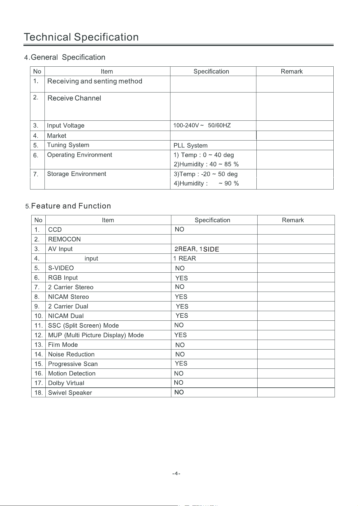
TOSHIBA CODE
Component
PAL SECAM / BG DK PAL / I
NTSC / M
VHF LOW K1~S6
VHF HIGH S7~S36
VHF S37~DS57
44.25MHz ~ 140.25MHz
147.25MHz ~ 423.25MHz
431.25MHz ~ 863.25MHz
Asia\Europe
Page 5
40
55
80
For 22” LED
For 24” LED
For 32” LED
Page 6

(24 inches is 4 ohm)
(24 inches is 3W)
Page 7
80
(26inches is 8 ohm)
40
40
3
2
1
4.2
50
0.5
12000
40
3
Page 8
Standard
Standard
20
40
NO
YES
8
6
46
46
NO
Spanish
Page 9
4
2
4
0 40 7 0
0 40 7 0
0 40
40 85
-Y 0 5 0
30000
Page 10
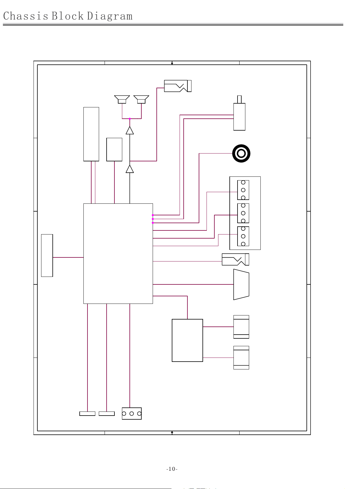
D
C
B
P12
SPEAKER
1
EARPHONE
TU2
TUNER
1
U29
U42
FLASH
2
M13S2561616A-5TG2K ESMT
U7 U1
TPA1517NE
SDA
SCL
P7
S/PDIP
2
3
4
LVDS OUT
U10
MST6E181VS
BH3544F-E2 TPA3113D2/
U19
PS331TQFP64G
P13
2P3P1P
P6
AV OUT
YPbPr AV2 INHDMI 1 VGA
PC
AUDIO
HDMI 2
3
4
MEDIA 2
5
AV1 IN
CON11
C
B
A A
D
CON10
CON6 MEDIA 1
5
Page 11
ʳ
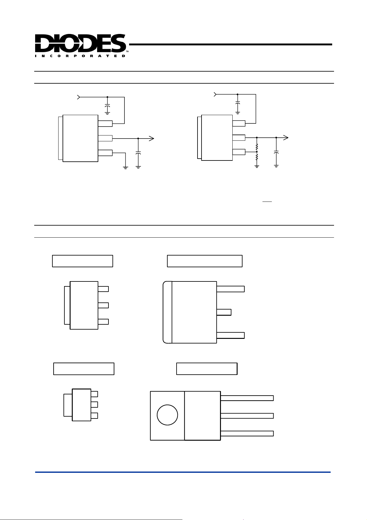
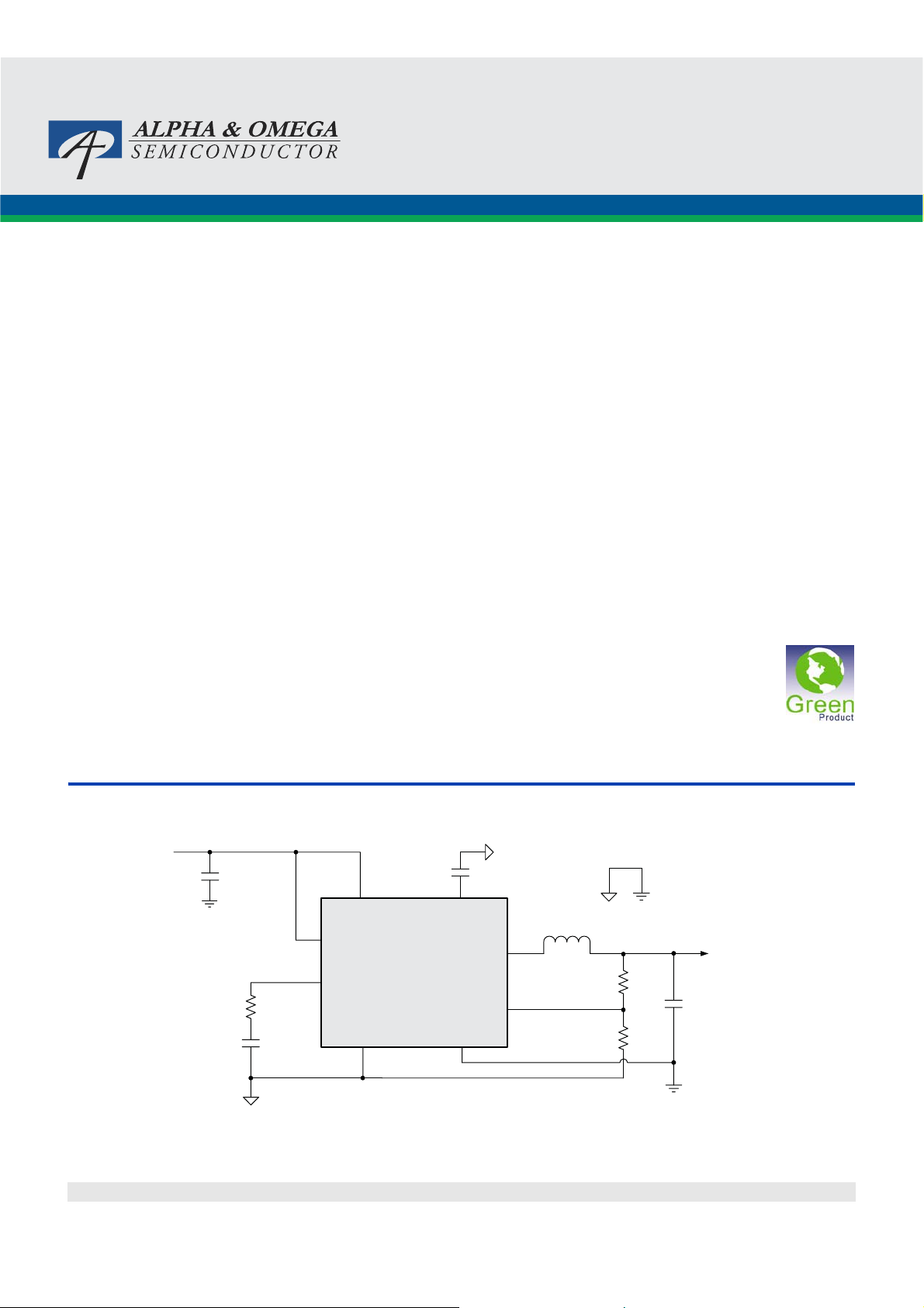
Typical Application Circuit ʳ
AP1117
1A LOW DROPOUT POSITIVE ADJUSTABLE OR
FIXED-MODE REGULATOR
5V
C1
10uF
V
in
V
out
GND
Tab is V
out
( 5V/3.3V fixed output ) ʳ
ʳ
Connection Diagramʳ
ʳ
ʳ
3 PIN SOT223 3 PIN TO252 / TO263
C2
22uF
3.3V/1A
5V
Tab is V
V
out
V
out
Adj
C1
10uF
in
( 5V/2.5V ADJ output ) ʳ
Note:
(1VV
REFo
R1
121
R2
121
R
R
V
o
2.5V/1A
C2
ȍ
22uF
ȍ
2
)
1
(
Top View )
3
2
1
Tab is V
out
3 PIN SOT89
3
2
1
Tab is V
out
V
in
V
out
Adj ( GND)
V
in
V
out
Adj ( GND)
(
Top View )
3
2
1
Tab is V
out
3 PIN TO220
3
2
1
Tab is V
out
V
V
out
Adj ( GND)
in
V
in
V
out
Adj ( GND)
ʳ
ʳ
AP1117 Rev. 3 2 of 11 SEPTEMBER 2006
www.diodes.com © Diodes Incorporated
Page 12
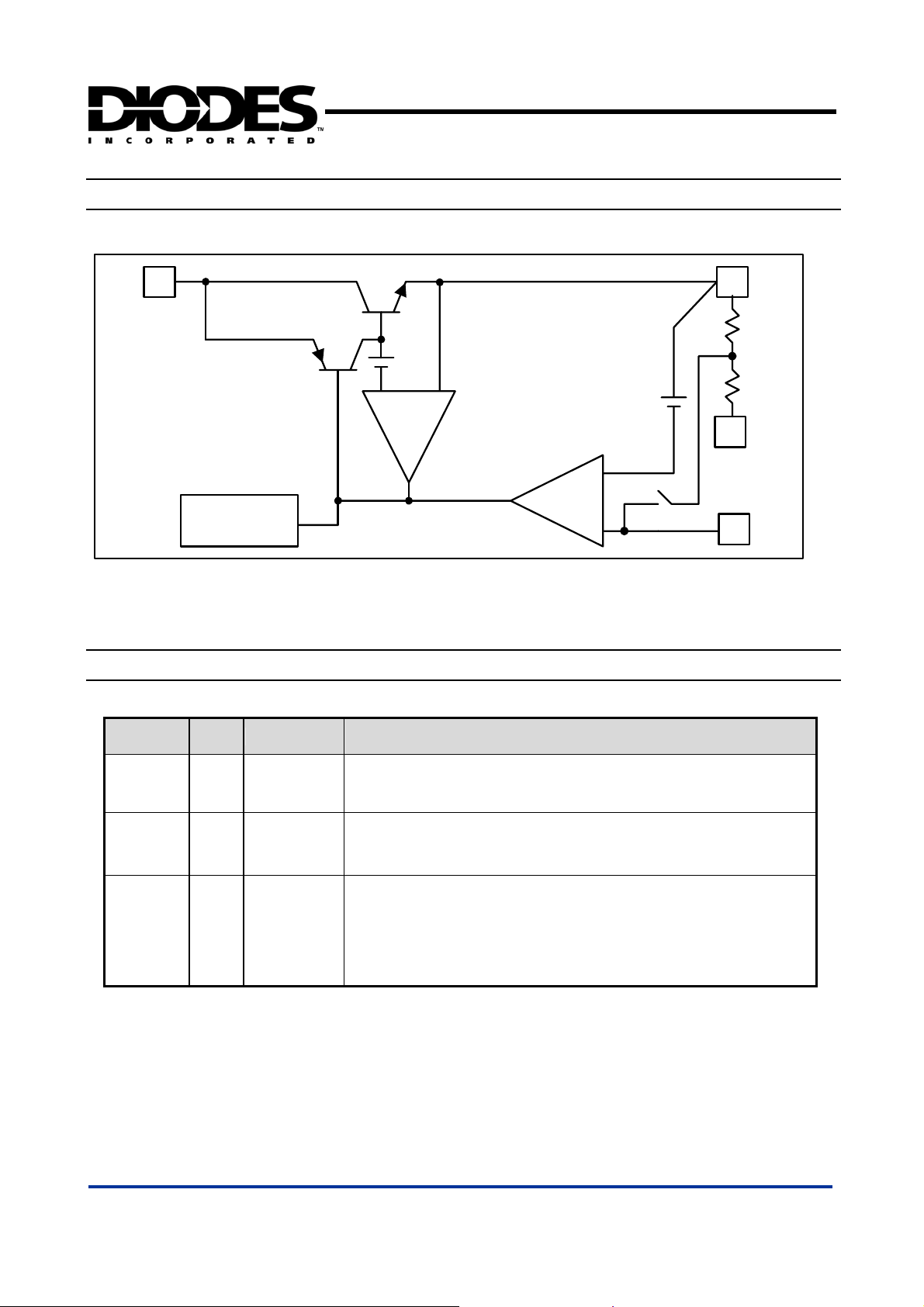
ʳ
Block Diagramʳ
AP1117
1A LOW DROPOUT POSITIVE ADJUSTABLE OR
FIXED-MODE REGULATOR
3
V
in
Thermal
Shutdown
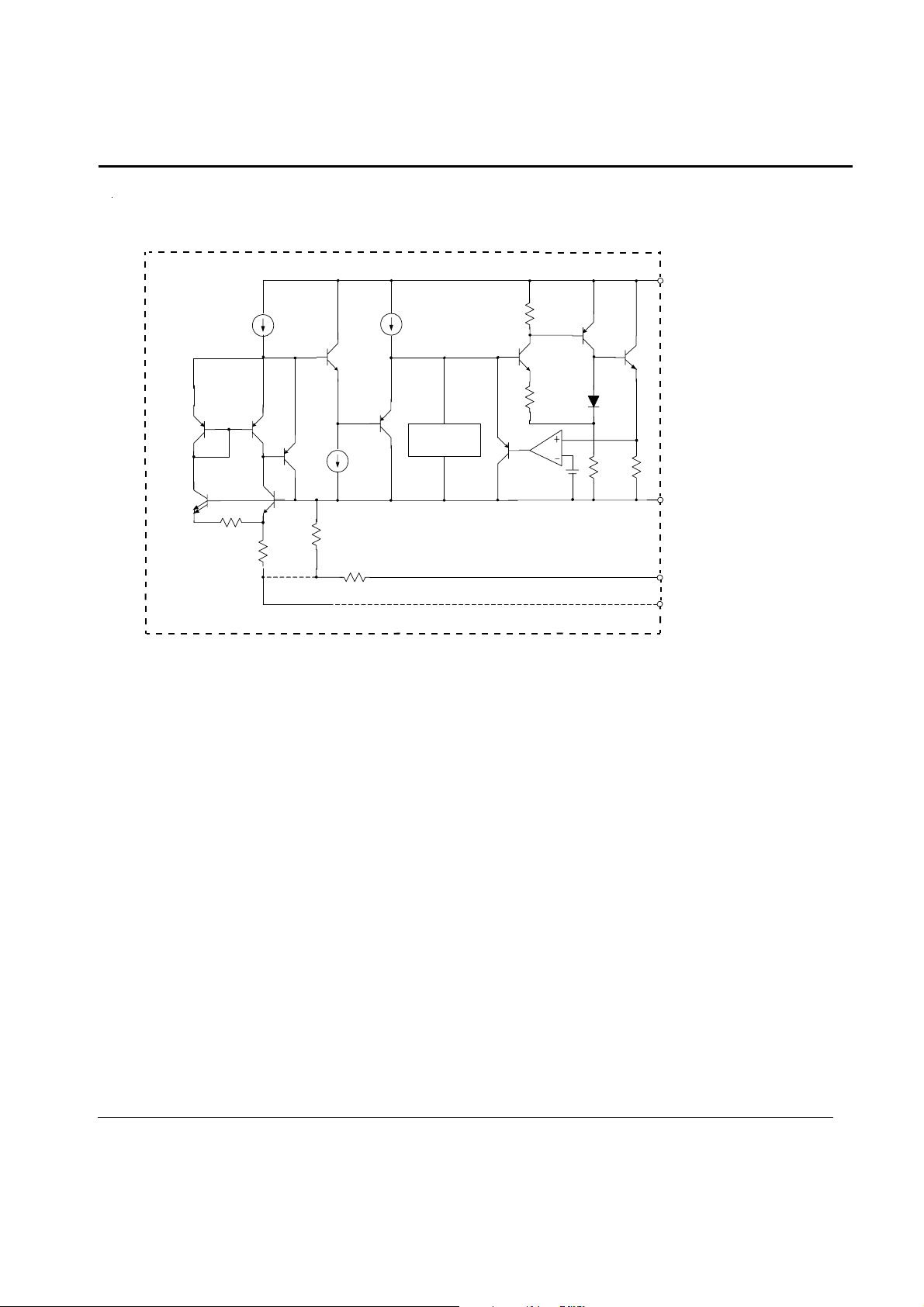
Pin Descriptionsʳ
2
V
out
+
+
-
1.25V
CURRENT
LIMIT
+
-
+
1
GND
(FIXED)
1
Adj
NAME I/O PIN # FUNCTION
Adj (GND) I 1
V
out
V
in
O 2
I 3
A resistor divider from this pin to the V
(Ground only for Fixed-Mode).
The output of the regulator. A minimum of 10uF capacitor (0.15ȍ ESR 20ȍ)
must be connected from this pin to ground to insure stability.
The input pin of regulator. Typically a large storage capacitor (0.15ȍ ESR 20ȍ)
is connected from this pin to ground to insure that the input voltage does not sag
below the minimum dropout voltage during the load transient response. This pin
must always be 1.3V higher than V
pin and ground sets the output voltage
out
in order for the device to regulate properly.
out
ʳ
AP1117 Rev. 3 3 of 11 SEPTEMBER 2006
www.diodes.com © Diodes Incorporated
Page 13
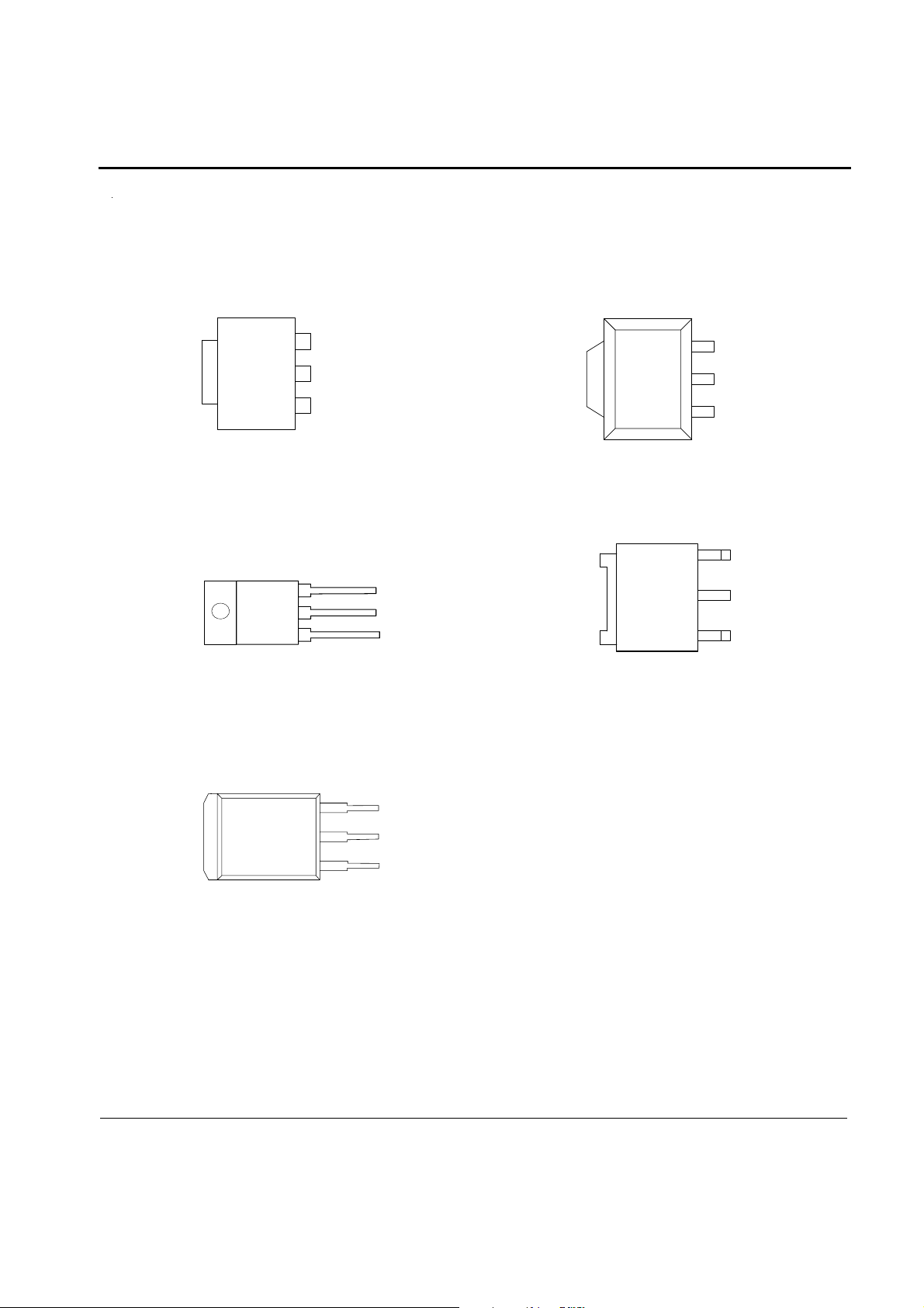
A1semi 1A Fixed and Adjustable Low
A1
A1
A1
Electronics Ltd Dropout Linear Regulator(LDO)
Pin Configurations
L Package
(SOT-223)
V
OUT
T Package
(TO-220) (TO-252)
AS1117
U Package
(SOT-89)
3
INPUT
2
OUTPUT
1
ADJ/GND
V
OUT
3
2
1
R Package
3
INPUT
OUTPUT
ADJ/GND
INPUT
V
OUT
S Package
(TO-263)
V
OUT
3
2
1
3
2
1
INPUT
OUTPUT
ADJ/GND
INPUT
OUTPUT
ADJ/GND
Figure 2. Pin Configurations of AS111 7
V
OUT
2
1
OUTPUT
ADJ/GND
AI SEMI ELECTRONICS LTD. 2
http://www.a1semi.com
Page 14
A1semi 1A Fixed and Adjustable Low
A1
A1
A1
Functional Block Diagram
Electronics Ltd Dropout Linear Regulator(LDO)
Thermal
Shutdown
AS1117
INPUT
Out
+
-
OUTPUT
GND (Fixed Output)
Figure 3. Functional Block Diagram of AS1117
ADJ (Adjustable Output)
A1 SEMI ELECTRONICS LTD. 3
http://www.a1semi.com
Page 15
AOZ1051PI
EZBuck™ 3 A Synchronous Buck Regulator
General Description
The AOZ1051PI is a high efficiency, easy to use, 3 A
synchronous buck regulator. The AOZ1051PI works from
4.5 V to 18 V input voltage range, and provides up to 3 A
of continuous output current with an output voltage
adjustable down to 0.8 V.
The AOZ1051PI comes in an exposed pad SO-8
package and is rated over a -40 °C to +85 °C operating
ambient temperature range.
Features
z 4.5 V to 18 V operating input voltage range
z Synchronous Buck: 70 m internal high-side switch
and 40 m internal low-side switch (at 12 V)
z Up to 95 % efficiency
z External soft start
z Output voltage adjustable to 0.8 V
z 3 A continuous output current
z 500 kHz PWM operation
z Cycle-by-cycle current limit
z Pre-bias start-up
z Short-circuit protection
z Thermal shutdown
z Exposed pad SO-8 package
Applications
z Point of load DC/DC converters
z LCD TV
z Set top boxes
z DVD and Blu-ray players/recorders
z Cable modems
Typical Application
VIN
C1
10μF
VIN
EN
AOZ1051PI
COMP
R
C
C
C
Figure 1. 3.3 V 3 A Synchronous Buck Regulator, Fs = 500 kHz
Rev. 1.0 June 2011 www.aosmd.com Page 1 of 14
AGND
SS
PGND
C
SS
L1 4.7μH
LX
R1
FB
R2
VOUT
C2, C3
22μF
Page 16

AOZ1051PI
A
Ordering Information
Part Number Ambient Temperature Range Package Environmental
AOZ1051PI -40 °C to +85 °C EPAD SO-8 Green Product
AOS Green Products use reduced levels of Halogens, and are also RoHS compliant.
Please visit www.aosmd.com/web/quality/rohs_compliant.jsp for additional information.
Pin Configuration
PGND
VIN
GND
FB
1
2
3
4
PAD
(LX)
8
NC
7
SS
6
EN
5
COMP
Exposed Pad SO-8
(Top View)
Pin Description
Pin Number Pin Name Pin Function
1 PGND Power ground. PGND needs to be electrically connected to AGND.
2 VIN Supply voltage input. When VIN rises above the UVLO threshold and EN is logic high,
the device starts up.
3 AGND Analog ground. AGND is the reference point for controller section. AGND needs to be
electrically connected to PGND.
4 FB Feedback input. The FB pin is used to set the output voltage via a resistive voltage divider
between the output and AGND.
5 COMP External loop compensation pin. Connect a RC network between COMP and AGND to
compensate the control loop.
6 EN Enable pin. Pull EN to logic high to enable the device. Pull EN to logic low to disable the
device. If on/off control in not needed, connect EN to VIN and do not leave it open.
7 SS Soft-start pin. 5 μA current charging current.
8 NC No Connect Pin. Pin 8 is not internally connected. Connect this pin externally to LX and
use it for better thermal performance.
Exposed pad LX Switching node. LX is the drain of the internal PFET. LX is used as the thermal pad of the
power stage.
Rev. 1.0 June 2011 www.aosmd.com Page 2 of 14
Page 17
Block Diagram
AOZ1051PI
VIN
EN
SS
FB
COMP
Reference
& Bias
0.8V
UVLO
& POR
+
EAmp
–
Softstart
5μA
SS
5V LDO
Regulator
Internal
+5V
+
PWM
–
Comp
+
500kHz
Oscillator
OTP
ILimit
PWM
Control
Logic
Level
Shifter
FET
Driver
AGND
+
ISen
–
Q1
+
LX
Q2
PGND
Absolute Maximum Ratings
Exceeding the Absolute Maximum Ratings may damage the
device.
Parameter Rating
Supply Voltage (VIN) 20 V
LX to AGND -0.7 V to V
LX to AGND (20 ns) -5 V to 22 V
EN to AGND -0.3 V to V
FB, SS, COMP to AGND -0.3 V to 6.0 V
PGND to AGND -0.3 V to +0.3 V
Junction Temperature (T
Storage Temperature (T
ESD Rating
Note:
1. Devices are inherently ESD sensitive, handling precautions are
required. Human body model rating: 1.5 k
Rev. 1.0 June 2011 www.aosmd.com Page 3 of 14
(1)
) +150 °C
J
) -65 °C to +150 °C
S
in series with 100 pF.
+0.3 V
IN
+0.3 V
IN
2.0 kV
Recommended Operating Conditions
The device is not guaranteed to operate beyond the Maximum
Recommended Operating Conditions.
Parameter Rating
Supply Voltage (VIN) 4.5 V to 18 V
Output Voltage Range 0.8 V to 0.85 • V
Ambient Temperature (TA) -40 °C to +85 °C
Package Thermal Resistance
Exposed Pad SO-8 (4
Note:
2. The value of
FR-4 board with 2 oz. Copper, in a still air environment with
T
= 25 °C. The value in any given application depends on the
A
user’s specific board design.
4
is measured with the device mounted on a 1-in
JA
JA
(2)
)
50 °C/W
IN
2
Page 18
SY8086
Package Code
Package Code
High Efficiency 1.4MHz, 1A
Synchronous Step Down Regulator
Preliminary Specification
General Description
The SY8086 is a high-efficiency 1.4MHz synchronous
step-down DC-DC regulator ICs capable of delivering
up to 1A output current. The SY8086 operates over a
wide input voltage range from 2.5V to 5.5V and
integrate main switch and synchronous switch with
very low R
Low output voltage ripple and s mall external indu ctor
and capacitor sizes are achieved with 1.4MHz
switching frequency. This along with small SOT-23
footprint prov ides small PCB area a pplication.
to minimize the conduction loss.
DS(ON)
Ordering Information
SY8086
SY8086
Temperature Range: -40
ƶƶƶƶ(ƶƶ
ƶƶ)ƶƶƶƶ
ƶƶƶƶ(ƶƶ
ƶƶ)ƶƶƶƶ
ƶƶƶƶ
ƶƶƶƶ
Temperature Code
Temperature Code
Optional Spec Code
Optional Spec Code
e
C to 85eC
Ordering Number Package type Note
SY8086AAC SOT23-5 1A
Featur es
•
Low R
250m
2.5-5.5V input voltage range
•
•
1.4MHz switching frequency minimizes the
external components
•
Internal softstart limits the inrush current
•
RoHS Compliant and Halogen Free
•
Compact package: SOT23 5 pin
for inter n al switche s (t op/ bottom):
DS(ON)
Ω
/200m
Ω
Applications
•
Portable Navigation Device
•
Smart phone
•
USB Dongle
•
Set Top Box
•
Media Player
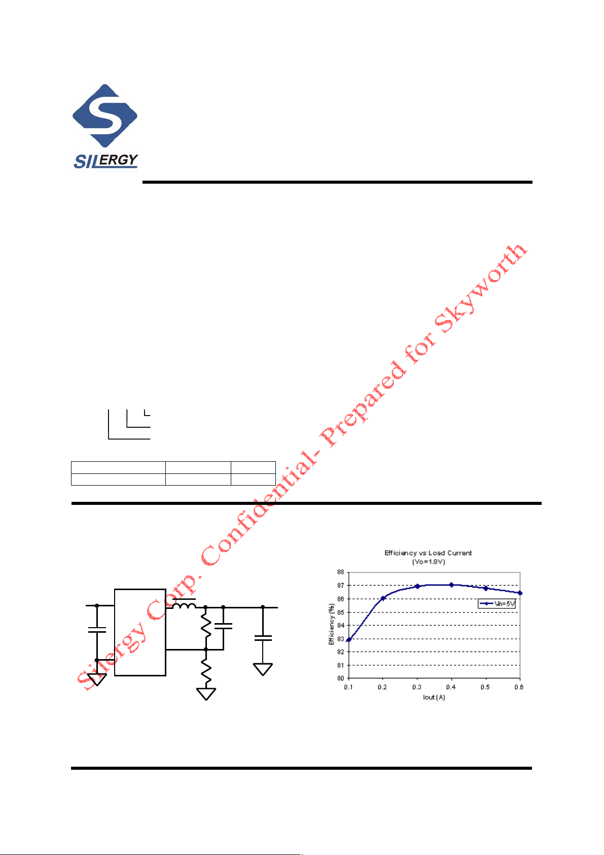
Typical Applications
V
IN
C
IN
EN
IN
LX
FB
GND
Figure 1. Schematic Diagram Figure2 Efficiency vs Load Current
SY8086 Rev. 0.11 Silergy Corp. Confidential- Prepared for Customer Use Only 1
L
R
R
C1(opt.)
1
2
V
OUT
C
OUT
Page 19
Pinout (top view)
SY8086
EN
EN
GND
GND
LX
LX
Top mark:
Pin Name Pin Number Pin Description
EN 1 Enable control. Pull high to turn on. Do not float.
GND 2 Ground pin
LX 3 Inductor pin. Connect this pin to the switching node of inductor
IN 4 Input pin. Decouple this pin to GND pin with at least 1uF ceramic cap
FB 5 Output Feedback Pin. Connect this pin to the center p oint of the output
BE
xyz
(Device code: BE, x=year code, y=wee k code , z = lot number code )
resistor divider (as shown in Figure 1) to progra m th e output voltage:
Vout=0.6*(1+R
Absolute Maximu m Ratings
Supply Input Voltage --------------------------------------------------------------------------------------------- 6.0V
Enable, FB Voltage------------------------------------------------------------------------------------------------ V
Power Dissipation, P
Package Thermal Resistance (Note 2)
SOT23-5,
SOT23-5,
Junction Temperature Range ------------------------------------------------------------------------------------ 150°C
Lead Temperature (Soldering, 10 sec.) ------------------------------------------------------------------------- 260°C
Storage Temperature Range ------------------------------------------------------------------------------------ESD Susceptibility (Note 2)
HBM (Human Body Mode) -------------------------------------------------------------------------------------- 2kV
MM (Machine Mode) ----------------------------------------------------------------------------------------------200V
D
@ TA = 25°C SOT-23-5 -------------------------------------------------------------- 0.4W
θ
JA
------------------------------------------------------------------------------------------ 250°C/W
θ
JC
-------------------------------------------------------------------------------------------130°C/W
1
1
2
2
3
3
SOT23-5
1/R2
(Note 1)
5
5
FB
FB
4
4
IN
IN
)
IN
+ 0.6V
-
65°C to 150°C
Recommended Operating Conditions
Supply Input Voltage -------------------------------------------------------------------------------------------- 2.5V to 5.5V
Junction Temperature Range ---------------------------------------------------------------------------------- -40°C to 125°C
Ambient Temperature Range ----------------------------------------------------------------------------------
(Note 3)
-
40°C to 85°C
SY8086 Rev. 0.11 Silergy Corp. Confidential- Prepared for Customer Use Only 2
Page 20
IC Block Diagram
U10(LCDTV CONTROLLER WITH VIDEO ECODE)MST6E181VS
PIN DIAGRAM (MST6E181VS)
162
161
160
159
158
157
156
155
154
153
152
151
150
149
148
147
146
145
144
143
142
141
140
139
138
137
136
135
134
133
132
131
130
129
NC
NC
LDQS0
LDQM0
A_DDR1_BA0
DVDD_DDR_1.2V
A_DDR1_DQ8
A_DDR1_DQ9
AVDDIO_2.5V
A_DDR1_DQ10
A_DDR1_DQ11
A_DDR1_DQ12
A_DDR1_DQ13
A_DDR1_DQ14
AVDDIO_2.5V
A_DDR1_DQ15
A_DDR1_MCLKZ
AVDDIO_2.5V
A_DDR1_MCLK
A_DDR1_CKE
A_DDR1_A12
A_DDR1_A11
A_DDR1_A9
AVDDIO_2.5V
A_DDR1_A8
A_DDR1_A7
A_DDR1_A6
A_DDR1_A5
A_DDR1_A4
AVDD_NODIE
DVDD_NODIE
GND_EFUSE
GPIO11/SAR0
GPIO12/SAR1
GPIO13/SAR2
GPIO10/PMGPIO
GPIO6/PM1/TX
GPIO8/PM5/RX
GPIO9/PM6/CS1
AVDDIO_2.5V
GPIO7/PM4/POWER_ON
163
164
165
166
167
168
169
170
171
172
173
174
175
176
177
178
179
180
181
182
183
184
185
186
187
188
189
190
191
192
193
194
195
196
197
198
199
200
201
202
203
204
205
206
207
208
209
210
211
212
213
214
215
216
217
AVDD_PLL
UDQM0
UDQS0
A_MVREF
NC
VDDC
DDCR_DA
VDDP_3
DDCR_CK
TESTPIN
DM_P0
DP_P0
DM_P1
DP_P1
SPI_CK
SPI_DI
SPI_DO
SPI_CZ
DDCA_CK
DDCA_DA
E-pad
AVDDIO_2.5V
A_DDR1_DQ4
A_DDR1_DQ7
A_DDR1_DQ6
A_DDR1_DQ5
AVDDIO_2.5V
A_DDR1_DQ3
A_DDR1_DQ2
A_DDR1_DQ1
A_DDR1_DQ0
AVDDIO_2.5V
A_DDR1_CAS
A_DDR1_RAS
A_DDR1_WEZ
A_DDR1_BA1
A_DDR1_A0
A_DDR1_A1
A_DDR1_A2
A_DDR1_A3
A_DDR1_A10
NC
NC
VDDC
VDDP_2
GPIO21/PWM1
GPIO20/PWM0
GPIO77/I2S_OUT_MUTE/PWM3/LVSYNC
MST6E181VS
128
127
126
125
124
123
122
121
120
119
118
117
116
115
VDDC
AVDD_LPLL
R_ODD7/RXO0-
R_ODD5/RXO1-
AVDD2P5_MOD
GPIO75/I2S_IN_SD/PWM5/TX3/LDE
GPIO74/I2S_IN_WS/PWM4/RX3/LCK
GPIO76/I2S_IN_BCK/PWM2/LHSYNC
R_ODD3/RXO2-
R_ODD1/RXOC-
R_ODD6/RXO0+
R_ODD4/RXO1+
R_ODD2/RXO2+
114
113
112
111
110
G_ODD3/RXE0-
G_ODD7/RXO3-
G_ODD5/RXO4-
G_ODD6/RXO3+
G_ODD4/RXO4+
R_ODD0/RXOC+
109
G_ODD2/RXE0+
AVDD2P5_MOD
108
G_ODD1/RXE1-
107
G_ODD0/RXE1+
106
B_ODD7/RXE2-
105
B_ODD6/RXE2+
104
B_ODD5/RXEC-
103
B_ODD4/RXEC+
102
B_ODD3/RXE3-
101
B_ODD2/RXE3+
100
B_ODD1/RXE4-
99
B_ODD0/RXE4+
98
NC
97
GPIO49
96
GPIO47
95
GPIO45
94
GPIO38
93
GPIO37
92
GPIO36
91
GPIO32/I2S_OUT_BCK
90
GPIO30/I2S_OUT_MCK
89
GPIO28
88
VDDP_1
87
VDDC
86
GPIO27/SPDIF_OUT
85
GPIO26/SPDIF_IN/RX1/PWM3
84
GPIO25/TUNER_SDA
83
GPIO24/TUNER_SCL
82
GPIO23/I2S_OUT_SD/TX2
81
GPIO22/I2S_OUT_WS/RX2
80
TAGC
79
SIFM
78
SIFP
77
AVDD25_PGA
76
VIFP
75
VIFM
74
AVSS_PGA
73
AVDD25_REF
72
AVDD_DMPLL
71
XTAL_OUT
70
XTAL_IN
69
NC
68
NC
67
NC
66
LINEOUT_R0
65
LINEOUT_L0
64
LINEOUT_R3
63
LINEOUT_L3
62
AVDD_AU33
61
LINEIN_R5
60
LINEIN_L5
59
LINEIN_R4
58
LINEIN_L4
57
LINEIN_R3
56
LINEIN_L3
55
U?
IRIN
2
1
9876543
10
RX1N
AVDD_DVI_3.3V
RX0P
RX0N
RXCP
RXCN
HOTPLUGA
RESET
CEC
HSYNC0
VDDC
NC
NC
SOGIN0
BIN0P
2726252423222120191817161514131211
GIN0M
GIN0P
VSYNC0
RIN0P
SOGIN1
BIN1P
AVDD2P5_ADC
AVDD1P2
GIN1P
GIN1M
CVBS2
CVBS3
CVBS4
AVDD3P3_ADC
RIN1P
CVBS0
CVBS1
4443424140393837363534333231302928
CVBS_OUT1
VCOM
45
LINEIN_L1
LINEIN_R0
LINEIN_L0
VRP
VRM
LINEIN_R1
AVDD_AU25
VAG
545352515049484746
NCNCNCNCNC
ARC
DDCDA_CK
RX2P
RX2N
DDCDA_DA
RX1P
-13-
Page 21
PDF "pdfFactory Pro" www.fineprint.cn
Page 22
PDF "pdfFactory Pro" www.fineprint.cn
Page 23
PDF "pdfFactory Pro" www.fineprint.cn
Page 24
PDF "pdfFactory Pro" www.fineprint.cn
Page 25
PDF "pdfFactory Pro" www.fineprint.cn
Page 26
PDF "pdfFactory Pro" www.fineprint.cn
Page 27
PDF "pdfFactory Pro" www.fineprint.cn
Page 28
MST6M181VG/MST6M182VG
2012010018
2012010018
LCD Television System-on-Chip
Preliminary Pin Diagram/Description and Mechanical Dimensions Version 0.2
Doc. No.:
PIN DIAGRAM (MST6M181VG/MST6M182VG)
1 2 3 4 5 6 7 8 9 10111213141516
A RXCKP RXCKN NC NC HWRESET GPIO7 GPIO6 GND USB1_DM USB0_DP USB0_DM A
B RX1N RX 0P RX0 N NC NC NC NC IRIN GPIO8 SAR0 PWM0 USB1_DP DDCR_CK SCZ SDO B
C RX2N RX2P RX1P NC NC NC NC GPIO9 SAR2 SA R1 PW M1 GND DDCR_DA SCK SDI C
D DDCD_CK ARC
ESOGIN0BIN0PHSYNC0
DDCD_DAHOTPLUG
A
NC CEC B YPASS
MStar Confidential
F RIN0P GIN0M GIN0P VSYNC0 GND
G GND GN D GND
for Skyworth
H SOGIN1 BIN1P
J RIN1P GIN1M GIN1P AVDD_33
K CV BS2 CVBS1 N C
Internal Use Only
L CVBS0 VCOM AUVAG AUVRP
M CVBSOU T AUL0 AUL3 GND
AVDD_AL
IVE
AVDD_D
MPLL
AVDD_ME
MPLL
AVDD_MODAVDD_ RE
AVDD_M
OD
AVDD_AU
33
AVDD_126DVDD_D
AVDD_25
AVDD_AU
VDDC VDDC GND GND GND
25
VDDC VDDC GND GND GND MVREF
F
VDDP VD DC VDDC FLK2 GCLK6 RLV2P L
VDDP
AVDD_D
DR
DR
AVDD_D
DDCA_CK DDC A_DA GPIO10 GND LEDON HCON DPM D
DR
GND GND GND
AVDD_ DDRAVDD_D
DR
AVDD_DDRSCAN_BL
GND SAR3 OPT_N GCLK4 G
K
SCAN_BL
K1
GSP/
VST
GSP_R/
GCLK1
VGH_OD
D
RLVCKM RLVCKP RLV2M M
GOE/
POL
GCLK2
WPWM OPT_P F
SOE FLK3 H
GSC/
GCLK 3
GCLK 5
FLK J
VGH_EVE
N
E
K
N AUR0 AUL1 AUR3 AUOUTL1
PAUR1 AUL2AUOUTR1 GND PGA_COM GND GND
RAUR2AUOUTL0 XOUT GND GND VIFM GND
T AUOUTR0 XIN TAGC GND VIFP GND
1 2 3 4 5 6 7 8 9 10111213141516
Doc. No.:
AVDD_PG
Copyright
GND NC NC RLV1M RLV1P RLV0M RLV0P RLV3M RLV3 P N
A
I2S_OUT
I2S_OUT
I2S_OUT
2011 MStar Semiconductor, Inc. All rights reserved.
SPDIFI LLV5M LLV4M LLV3P LLV2M LLV1M RLV4M RLV4 P P
_SD
I2S_OUT
_MCK
_BCK
SPDIFO LLV3M LLVCKM LLV0M LLV0P T
_WS
- 1 - 8/29/2011
PDF "pdfFactory Pro" www.fineprint.cn
LLV5P LLV4P LLV CKP LLV2P LLV1P RLV5 M RLV5 P R
Page 29
MST6M181VG/MST6M182VG
2012010018
2012010018
LCD Television System-on-Chip
Preliminary Pin Diagram/Description and Mechanical Dimensions Version 0.2
Doc. No.:
PIN DESCRIPTION
Analog Interface
Pin Name Pin Type Function Pin
HSYNC0 Schmitt Trigger Input
w/ 5V-tolerant
VSYNC0 Schmitt Trigger Input
w/ 5V-tolerant
BIN0P Analog Input Analog Blue Input from Channel 0 E3
SOGIN0 Analog Input Sync On Green Input from Channel 0 E2
GIN0P Analog Input Analog Green Input from Channel 0 F3
GIN0M Analog Input Reference Ground for Analog Green Input from Channel 0 F2
RIN0P Analog Input Analog Red Input from Channel 0 F1
MStar Confidential
BIN1P Analog Input Analog Blue Input from Channel 1 H3
SOGIN1 Analog Input Sync On Green Input from Channel 1 H2
GIN1P Analog Input Analog Green Input from Channel 1 J3
GIN1M Analog Input Reference Ground for Analog Green Input from Channel 1 J2
RIN1P Analog Input Analog Red Input from Channel 1 J1
HSYNC / Composite Sync for VGA Input from channel 0 E4
VSYNC for VGA Input from channel 0 F4
for Skyworth
Analog Video Input/Output Interface
Pin Name Pin Type Function Pin
CVBS2 Analog Input CVBS (Composite) Video Input Channel 2 K1
CVBS1 Analog Input CVBS (Composite) Video Input Channel 1 K2
Internal Use Only
CVBS0 Analog Input CVBS (Composite) Video Input Channel 0 L1
VCOM Analog Input CVBS Input Reference Ground L2
CVBSOUT Analog Output CVBS (Composite) Video Output Channel M1
Analog Audio Input/Output Interface
Pin Name Pin Type Function Pin
I2S_OUT_WS I/O w/ 5V-tolerant Word Select Output; 4mA driving strength /
Universal Asynchronous Receiver 2 (UART2_RX)
I2S_OUT_SD I/O w/ 5V-tolerant Audio Serial Data Output; 4mA driving strength /
Universal Asynchronous Transmitter 2 (UART2_TX)
SPDIFI Input w/ 5V-tolerant S/PDIF Audio Input /
Pulse Width Modulation Output; 4mA driving strength
(PWM3)
SPDIFO Output S/PDIF Audio Output; 4mA driving strength T9
Doc. No.:
Copyright
2011 MStar Semiconductor, Inc. All rights reserved.
- 2 - 8/29/2011
T8
P8
P9
PDF "pdfFactory Pro" www.fineprint.cn
Page 30
MST6M181VG/MST6M182VG
2012010018
2012010018
LCD Television System-on-Chip
Preliminary Pin Diagram/Description and Mechanical Dimensions Version 0.2
Doc. No.:
Pin Name Pin Type Function Pin
I2S_OUT_MCK Output w/ 5V-tolerant Audio Master Clock Output R8
I2S_OUT_BCK Output w/ 5V-tolerant Audio Bit Clock Output R9
AUL0 Analog Input Audio Line Input Left Channel 0 M2
AUR0 Analog Input Audio Line Input Right Channel 0 N1
AUL1 Analog Input Audio Line Input Left Channel 1 N2
AUR1 Analog Input Audio Line Input Right Channel 1 P1
AUL2 Analog Input Audio Line Input Left Channel 2 P2
AUR2 Analog Input Audio Line Input Right Channel 2 R1
AUL3 Analog Input Audio Line Input Left Channel 3 M3
AUR3 Analog Input Audio Line Input Right Channel 3 N3
AUVRP Analog Output Positive Reference Voltage for Audio ADC L4
MStar Confidential
AUVAG Analog Output Reference Voltage for Audio Common Mode L3
AUOUTL1 Analog Output Main Audio Output Left Channel 1 N4
AUOUTR1 Analog Output Main Audio Output Right Channel 1 P3
AUOUTL0 Analog Output Main Audio Output Left Channel 0 R2
AUOUTR0 Analog Output Main Audio Output Right Channel 0 T2
for Skyworth
Mini-LVDS Interface
Pin Name Pin Type Function Pin
LLV5M Output Mini-LVDS L-Link Channel 5 Negative Data Output P10
LLV5P Output Mini-LVDS L-Link Channel 5 Positive Data Output R10
Internal Use Only
LLV4M Output Mini-LVDS L-Link Channel 4 Negative Data Output P11
LLV4P Output Mini-LVDS L-Link Channel 4 Positive Data Output R11
LLV3M Output Mini-LVDS L-Link Channel 3 Negative Data Output T11
LLV3P Output Mini-LVDS L-Link Channel 3 Positive Data Output P12
LLV2M Output Mini-LVDS L-Link Channel 2 Negative Data Output P13
LLV2P Output Mini-LVDS L-Link Channel 2 Positive Data Output R13
LLV1M Output Mini-LVDS L-Link Channel 1 Negative Data Output P14
LLV1P Output Mini-LVDS L-Link Channel 1 Positive Data Output R14
LLV0M Output Mini-LVDS L-Link Channel 0 Negative Data Output T14
LLV0P Output Mini-LVDS L-Link Channel 0 Positive Data Output T15
LLVCKM Output Mini-LVDS L-Link Negative Clock Output T12
LLVCKP Output Mini-LVDS L-Link Positive Clock Output R12
RLV5M Output Mini-LVDS R-Link Channel 5 Negative Data Output R15
RLV5P Output Mini-LVDS R-Link Channel 5 Positive Data Output R16
Doc. No.:
Copyright
PDF "pdfFactory Pro" www.fineprint.cn
2011 MStar Semiconductor, Inc. All rights reserved.
- 3 - 8/29/2011
Page 31

MST6M181VG/MST6M182VG
2012010018
2012010018
LCD Television System-on-Chip
Preliminary Pin Diagram/Description and Mechanical Dimensions Version 0.2
Doc. No.:
Pin Name Pin Type Function Pin
RLV4M Output Mini-LVDS R-Link Channel 4 Negative Data Output P15
RLV4P Output Mini-LVDS R-Link Channel 4 Positive Data Output P16
RLV3M Output Mini-LVDS R-Link Channel 3 Negative Data Output N14
RLV3P Output Mini-LVDS R-Link Channel 3 Positive Data Output N15
RLV2M Output Mini-LVDS R-Link Channel 2 Negative Data Output M16
RLV2P Output Mini-LVDS R-Link Channel 2 Positive Data Output L16
RLV1M Output Mini-LVDS R-Link Channel 1 Negative Data Output N10
RLV1P Output Mini-LVDS R-Link Channel 1 Positive Data Output N11
RLV0M Output Mini-LVDS R-Link Channel 0 Negative Data Output N12
RLV0P Output Mini-LVDS R-Link Channel 0 Positive Data Output N13
RLVCKM Output Mini-LVDS R-Link Negative Clock Output M14
MStar Confidential
RLVCKP Output Mini-LVDS R-Link Positive Clock Output M15
TCON Interface
Pin Name Pin Type Function Pin
POL Output Polarity Control Single E15
SOE Output Source Output Enable H15
GSP/
VST
GCLK6 Output Gate Clock for GIP Panel L15
GCLK5 Output Gate Clock for GIP Panel K15
Internal Use Only
GCLK4 Output Gate Clock for GIP Panel G16
GSC/
GCLK3
GOE/
GCLK2
GSP_R/
GCLK1
SCAN_BLK1 Output Scan Backlight Control Signal 1 F14
SCAN_BLK Output Scan Backlight Control Signal E14
OPT_N Output The Output Pin to Indicate Reverse State G15
for Skyworth
Output Gate Start Pulse for LTD Panel /
Vertical start pulse for GIP Panel
Output Gate Shift Clock for LTD Panel /
Gate Clock for GIP Panel
Output Gate Clock for GIP Panel /
Gate Output Enable for LTD Panel
Output Right Gate Start Pulse for LTD Panel /
Gate Clock for GIP Panel
H14
J15
E16
J14
OPT_P Output The Output Pin to Indicate Reverse State F16
FLK3 Output Gate Modulation Signal H16
FLK2 Output Gate Modulation Signal L14
FLK Output Gate Modulation Signal J16
Doc. No.:
Copyright
2011 MStar Semiconductor, Inc. All rights reserved.
- 4 - 8/29/2011
PDF "pdfFactory Pro" www.fineprint.cn
Page 32

MST6M181VG/MST6M182VG
2012010018
2012010018
LCD Television System-on-Chip
Preliminary Pin Diagram/Description and Mechanical Dimensions Version 0.2
Doc. No.:
Pin Name Pin Type Function Pin
WPWM Output PWM Output for Wavy Noise F15
HCON Output H Inversion Control Signal on DPC D15
DPM Output Power Sequence Control Signal D16
LEDON Output LED On D14
VGH_ODD Output VGH Odd for GIP Panel K14
VGH_EVEN Output VGH Even for GIP Pane K16
DVI/HDMI Interface
Pin Name Pin Type Function Pin
RXCKN DVI/HDMI Input Negative DVI/HDMI Input for A Link Clock Channel A3
RXCKP DVI/HDMI Input Positive DVI/HDMI Input for A Link Clock Channel A2
MStar Confidential
RX0N DVI/HDMI Input Negative DVI/HDMI Input for A Link Data Channel 0 B3
RX0P DVI/HDMI Input Positive DVI/HDMI Input for A Link Data Channel 0 B2
RX1N DVI/HDMI Input Negative DVI/HDMI Input for A Link Data Channel 1 B1
RX1P DVI/HDMI Input Positive DVI/HDMI Input for A Link Data Channel 1 C3
RX2N DVI/HDMI Input Negative DVI/HDMI Input for A Link Data Channel 2 C1
RX2P DVI/HDMI Input Positive DVI/HDMI Input for A Link Data Channel 2 C2
ARC DVI/HDMI Output Audio Return Channel D2
for Skyworth
Serial Flash Interface
Internal Use Only
Pin Name Pin Type Function Pin
SCK
SDI
SDO Input w/ 5V-tolerant SPI Flash Serial Data Output B16
SCZ
IRIN Input w/ 5V-tolerant IR Receiver Input B9
Output
Output
Output
SPI Flash Serial Clock C15
SPI Flash Serial Data Input C16
SPI Flash Chip Select B15
GPIO Interface
Pin Name Pin Type Function Pin
GPIO10 I/O w/ 5V-tolerant
GPIO9 I/O w/ 5V-tolerant General Purpose Input/Output; 4mA driving strength C9
GPIO8 I/O w/ 5V-tolerant General Purpose Input/Output /
GPIO7 I/O w/ 5V-tolerant General Purpose Input/Output; 4mA driving strength
Doc. No.:
Copyright
General Purpose Input/Output; 4mA driving strength
Universal Asynchronous Receiver 0 (UART0_RX)
For Power Management Only
- 5 - 8/29/2011
2011 MStar Semiconductor, Inc. All rights reserved.
PDF "pdfFactory Pro" www.fineprint.cn
D12
B10
A10
Page 33

MST6M181VG/MST6M182VG
2012010018
2012010018
LCD Television System-on-Chip
Preliminary Pin Diagram/Description and Mechanical Dimensions Version 0.2
Doc. No.:
Pin Name Pin Type Function Pin
GPIO6 I/O w/ 5V-tolerant General Purpose Input/Output /
Word Select Output; 4mA driving strength (I2S_OUT_WS) /
Universal Asynchronous Transmitter 0 (UART0_TX)
PWM1 Output w/ 5V-tolerant Pulse Width Modulation Output; 4mA driving strength C12
PWM0 Output w/ 5V-tolerant Pulse Width Modulation Output; 4mA driving strength B12
SAR3 Analog Input SAR Low Speed ADC Input 3 G14
SAR2 Analog Input SAR Low Speed ADC Input 2 C10
SAR1 Analog Input SAR Low Speed ADC Input 1 C11
SAR0 Analog Input SAR Low Speed ADC Input 0 B11
A11
USB Interface
MStar Confidential
Pin Name Pin Type Function Pin
USB0_DP Analog I/O USB Non Inverting Data Input/Output for Port 0 A14
USB0_DM Analog I/O USB Inverting Data Input/Output for Port 0 A15
USB1_DP Analog I/O USB Non Inverting Data Input/Output for Port 1 B13
USB1_DM Analog I/O USB Inverting Data Input/Output for Port 1 A13
for Skyworth
VIF Interface
Pin Name Pin Type Function Pin
VIFM Analog Input Negative Video IF Input R6
VIFP Analog Input Positive Video IF Input T6
Internal Use Only
TAGC Analog Output Tuner Automatic Gain Control Output T4
PGA_COM Analog Input VIF PGA Negative Source P5
Misc. Interface
Pin Name Pin Type Function Pin
HWRESET Schmitt Trigger Input
w/ 5V-tolerant
DDCD_DA I/O w/ 5V-tolerant HDCP Serial Bus Data / DDC Data of DVI/HDMI D3
DDCD_CK Input w/ 5V-tolerant HDCP Serial Bus Clock / DDC Clock of DVI/HDMI D1
DDCR_DA I/O w/ 5V-tolerant DDC Data for ROM C14
DDCR_CK Input w/ 5V-tolerant DDC Clock for ROM B14
HOTPLUGA I/O w/ 5V-tolerant Hot-plug control for DVI/HDMI D4
DDCA_DA I/O w/ 5V-tolerant DDC Data for Analog port D11
Hardware Reset; active high A9
DDCA_CK I/O w/ 5V-tolerant DDC Clock for Analog port D10
Doc. No.:
Copyright
PDF "pdfFactory Pro" www.fineprint.cn
2011 MStar Semiconductor, Inc. All rights reserved.
- 6 - 8/29/2011
Page 34

MST6M181VG/MST6M182VG
2012010018
2012010018
LCD Television System-on-Chip
Preliminary Pin Diagram/Description and Mechanical Dimensions Version 0.2
Doc. No.:
Pin Name Pin Type Function Pin
XIN Crystal Oscillator Input Crystal Oscillator Input T3
XOUT Crystal Oscillator
Output
BYPASS For External Bypass Capacitor D7
CEC I/O Consumer Electronics Control D6
MVREF Input Reference Voltage for DDR SDRAM Interface K13
Crystal Oscillator Output R3
Power Pins
Pin Name Pin Type Function Pin
AVDD_33 3.3V Power Analog 3.3V Power J4
AVDD_25 2.5V Power Analog 2.5V Power H6
MStar Confidential
AVDD_126 1.26V Power Analog 1.26V Power H7
AVDD_AU25 2.5V Power Audio 2.5V Power J6
AVDD_AU33 3.3V Power Audio 3.3V Power M5
AVDD_DMPLL 3.3V Power Crystal Power K4
AVDD_REF 2.5V Power Demod ADC Power K6
AVDD_PGA 2.5V Power Demod PGA Power N5
AVDD_MOD 3.3V Power MOD Power K5, L5
AVDD_MEMPLL 3.3V Power PLL Power J5
AVDD_DDR 1.8V Power DDR Power D9, E13, G8, M10, M11
for Skyworth
DVDD_DDR 1.26V Power DDR 1.26V Power H8
Internal Use Only
AVDD_ALIVE 3.3V Power Alive Domain IO Power H4
VDDC 1.26V Power Digital Core Power J7, J8, K7, K8, L7, L8
VDDP 3.3V Power Digital Input/Output Power L6, M6
GND Ground Ground A12, C13, D13, F13, G1-G3, G13,
H9-H11, J9-J11, K9-K11, M4, N6, P4,
P6, P7, R4, R5, R7, T5, T7
No Connects
Pin Name Pin Type Function Pin
NC No connect A5, A6, B4-B7, C4-C7, D5, K3, N8, N9
Doc. No.:
Copyright
2011 MStar Semiconductor, Inc. All rights reserved.
- 7 - 8/29/2011
PDF "pdfFactory Pro" www.fineprint.cn
Page 35

MST6M181VG/MST6M182VG
prop
malfunctio
performance degradation.
2012010018
2012010018
LCD Television System-on-Chip
Preliminary Pin Diagram/Description and Mechanical Dimensions Version 0.2
Doc. No.:
DISCLAIMER
MSTAR SEMICONDUCTOR RESERVES THE RIGHT TO MAKE CHANGES WITHOUT FURTHER NOTICE
TO ANY PRODUCTS HEREIN TO IMPROVE RELIABILITY, FUNCTION OR DESIGN. NO
RESPONSIBILITY IS ASSUMED BY MSTAR SEMICONDUCTOR ARISING OUT OF THE APPLICATION
OR USER OF ANY PRODUCT OR CIRCUIT DESCRIBED HEREIN; NEITHER DOES IT CONVEY ANY
LICENSE UNDER ITS PATENT RIGHTS, NOR THE RIGHTS OF OTHERS.
Electrostatic charges accumulate on both test equipment and human bodyand can dischargewithout
detection. MST6M181VG/MST6M182VG comes with ESD protection circuitry; however, the device
may be permanently damaged when subjected to high energy discharges. The device should be
handled with
er ESDprecautions toprevent
nand
REVISION HISTORY
Document Description Date
MST6M181VG/MST6M182VG_pin_v01 Initial release Aug 2011
MST6M181VG/MST6M182VG_pin_v02 Added Ball Diameter to Mechanical Dimensions Aug 2011
MStar Confidential
for Skyworth
Internal Use Only
Doc. No.:
Copyright
PDF "pdfFactory Pro" www.fineprint.cn
2011 MStar Semiconductor, Inc. All rights reserved.
- 8 - 8/29/2011
Page 36

Preliminary Pin Diagram/Description and Mechanical Dimensions Version 0.2
2012010018
2012010018
Doc. No.:
MECHANICAL DIMENSIONS
MST6M181VG/MST6M182VG
LCD Television System-on-Chip
D
E
M
S
MStar Confidential
A1
A
10
12
14
16
15
11
13
82
7
for Skyworth
Internal Use Only
E1
e
4
6
5
19
3
A
B
C
D
E
F
G
H
J
K
L
M
N
P
R
T
Symbol
A - - 1.40 - - 0.055
A1 0.27 - 0.37 0.011 - 0.015
M 0.70 REF 0.028 REF
S 0.22 0.26 0.30 0.009 0.010 0.012
D - 13.50 - - 0.531 -
E - 13.50 - - 0.531 -
D1 - 12.00 - - 0.472 -
E1 - 12.00 - - 0.472 -
e - 0.80 - - 0.031 -
Ball
Diameter
Millimeter Inch
Min. Nom. Max. Min. Nom. Max.
- 0.40 - - 0.016 -
b (200x)
- 9 - 8/29/2011
Doc. No.:
e
D1
Copyright
2011 MStar Semiconductor, Inc. All rights reserved.
PDF "pdfFactory Pro" www.fineprint.cn
Page 37

IC Block Diagram
8᧤0%,7&0266(5,$/)/$6+᧥623
Address
Generator
MemoryArray
P age B uffer
SI/SIO0
SO /SIO1
CS#,
WP#,
HOLD#
S CLK Clock G enerator
Data
Register
SRAM
B uffer
M ode
Logic
S tate
Machine
Y-D ecoder
Sense
Am plifier
HV
Generator
Output
B uffer
-15-
Page 38

IC Block Diagram
U19(HDMI SWITCH) PS331TQFP64G
SiI9185 Pin Mapping
POW_SINK
HPD3
SDA3
SCL3
B31
A31
POW3
B32
A32
GND
B33
A33
VCC
B34
A34
CEXT
49
50
51
52
53
54
55
56
57
58
59
60
61
62
63
64
SDA_SINK
48 47
Z1
SCL_SINK
46
HPD_SINK
Y1
Y2
Z2
45 44 43 42 41
GND
Z4
Z3
Y3
VCC
Y4
PS331
1
2 3 4 5 6 7 8 9 10 11 12 13 14 15 16
I2C_ADDR
SCL_CTL
SDA_CTL
3334353637383940
POWDN
32
31
30
29
28
27
26
25
24
23
22
21
20
19
18
17
REXT
A14
B14
NC
A13
B13
GND
A12
B12
VCC
A11
B11
SCL1
SDA1
I2C_RST
B21
SDA2
HPD2
SCL2
A21
B22
POW2
A22
GND
B23
A23
B24
VCC
A24
HPD1
POW1
-16-
Page 39

)RU6N\ZRUWK(YDOXDWLRQ2QO\
Parade Technologies Inc.
PS331 HDMI/DVI SWITCH
Table1. Pin Descriptions
Name I/O Description
Axy I x = 1, 2, 3 for TMDS input channel number
y = 1, 2, 3, 4 for TMDS positive differential data or clock inputs
Bxy I x = 1, 2, 3 for TMDS input channel number
y = 1, 2, 3, 4 for TMDS negative differential data or clock inputs
Yx O x = 1, 2, 3, 4 for TMDS positive differential outputs
Zx O x = 1, 2, 3, 4 for TMDS negative differential outputs
HPDx O x = 1, 2, 3 for Hot Plug Detection output to source devices
HPD_SINK I Hot Plug Detection input from sink device; internal pull-down at ~80K ohm
Each port’s HPD can be set independently by I2C registers. See the Register Definition Table for
details
SCLx, SDAx I/O SCLx: I2C bus clock lines, SDAx: I2C bus data lines; x = 1, 2, 3; 5 V tolerant; internal pull-down
at ~1.1M ohm
SCL_SINK I/O Sink side I2C clock line
SDA_SINK I/O Sink side I2C data line
I
SDA_CTL
SCL_CTL
I2C_ADDR
REXT I Bias Current setting by External resistor, 500 ohm 1% to GND
POW_SINK O A 3.3 V CMOS output which indicates the selected port being connected to the corresponding
I2C_RST
POWDN
POW1
POW2
POW3
CEXT I/O An external capacitor is connected for supply regulation.
GND Ground connection
VCC Power supply at 3.3 V
TEL: 408-329-5540
FAX: 408-329-5541
Email: Sales@paradetech.com
I2C_ADDR: I2C control bus address LSB
SDA_CTL: I2C control data; SCL_CTL: I2C control clock
SCL_CTL / SDA_CTL control is described in the Register Definition Table
Source port
POW_SINK is the status for the selected Port Source Connection Detection. When the selected
port 5 V Source Supply is detected, POW_SINK will output HIGH to indicate the Source is
connected
For each port, the Port Source Connection status can also be accessed by I2C registers
I/O I2C_RST assertion will reset the I2C control logic; POWDN assertion will power down the chip.
PS331 power-on reset and subsequent operation are controlled automatically by on-chip
configuration logic. There is usually no need to reset the I2C control logic unless for the system
debugging and development purpose. The power down control provides a tool for system to
manage the PS331 power for power sensitive applications
I Source Connection Detection Inputs
These pins shall be connected to HDMI connector Source DC 5 V supply pins through a 37K
ohm resistor respectively. If the Source Connection Detection is not used, these pins shall be
connected to local VCC (3.3 V)
The Source Connection Detection status for each port is accessible through I2C registers
The capacitor should be 2.2 uF or larger for power noise filtering
For Customer Internal Use Only 7
Page 40

TAS5707
SLOS556A–NOVEMBER 2008 –REVISED APRIL 2009 .................................................................................................................................................
48-TERMINAL, HTQFP PACKAGE (TOP VIEW)
PHP Package
(Top View)
PVDD_B
OUT_A
PVDD_A
PVDD_A
BST_A
GVDD_OUT
SSTIMER
OC_ADJ
NC
AVSS
PLL_FLTM
PLL_FLTP
VR_ANA
484746
1
2
3
4
5
6
7
8
9
10
11
12
13
PVDD_B
PGND_AB
PGND_AB
OUT_B
45 44
15 161718 19 20
14
BST_B
43 42 41 40 39 38 37
TAS5707
BST_C
PVDD_C
PVDD_C
PGND_CD
OUT_C
21 222324
PGND_CD
36
35
34
33
32
31
30
29
28
27
26
25
OUT_D
PVDD_D
PVDD_D
BST_D
GVDD_OUT
VREG
AGND
GND
DVSS
DVDD
STEST
RESET
www.ti.com
AVDD
FAULT
MCLK
OSC_RES
DVSSO
VR_DIG
PDN
LRCLK
SCLK
SDIN
SDA
P0075-01
SCL
PIN FUNCTIONS
PIN
NAME NO.
AGND 30 P Analog ground for power stage
AVDD 13 P 3.3-V analog power supply
AVSS 9 P Analog 3.3-V supply ground
BST_A 4 P High-side bootstrap supply for half-bridge A
BST_B 43 P High-side bootstrap supply for half-bridge B
BST_C 42 P High-side bootstrap supply for half-bridge C
BST_D 33 P High-side bootstrap supply for half-bridge D
DVDD 27 P 3.3-V digital power supply
DVSSO 17 P Oscillator ground
DVSS 28 P Digital ground
GND 29 P Analog ground for power stage
GVDD_OUT 5, 32 P Gate drive internal regulator output
LRCLK 20 DI 5-V Pulldown Input serial audio data left/right clock (sample rate clock)
MCLK 15 DI 5-V Pulldown Master clock input
(1) TYPE: A = analog; D = 3.3-V digital; P = power/ground/decoupling; I = input; O = output
(2) All pullups are weak pullups and all pulldowns are weak pulldowns. The pullups and pulldowns are included to assure proper input logic
levels if the pins are left unconnected (pullups ĺ logic 1 input; pulldowns ĺ logic 0 input).
6 Submit Documentation Feedback
TYPE 5-V TERMINATION
(1)
TOLERANT
(2)
Product Folder Link(s): TAS5707
DESCRIPTION
Copyright © 2008–2009, Texas Instruments Incorporated
Page 41

TAS5707
www.ti.com
................................................................................................................................................. SLOS556A –NOVEMBER 2008 –REVISED APRIL 2009
PIN FUNCTIONS (continued)
PIN
NAME NO.
NC 8 – No connection
OC_ADJ 7 AO Analog overcurrent programming. Requires resistor to ground.
OSC_RES 16 AO Oscillator trim resistor. Connect an 18.2-k 1% resistor to DVSSO.
OUT_A 1 O Output, half-bridge A
OUT_B 46 O Output, half-bridge B
OUT_C 39 O Output, half-bridge C
OUT_D 36 O Output, half-bridge D
PDN
PGND_AB 47, 48 P Power ground for half-bridges A and B
PGND_CD 37, 38 P Power ground for half-bridges C and D
PLL_FLTM 10 AO PLL negative loop filter terminal
PLL_FLTP 11 AO PLL positive loop filter terminal
PVDD_A 2, 3 P Power supply input for half-bridge output A
PVDD_B 44, 45 P Power supply input for half-bridge output B
PVDD_C 40, 41 P Power supply input for half-bridge output C
PVDD_D 34, 35 P Power supply input for half-bridge output D
RESET
SCL 24 DI 5-V I
SCLK 21 DI 5-V Pulldown Serial audio data clock (shift clock). SCLK is the serial audio port input
SDA 23 DIO 5-V I
SDIN 22 DI 5-V Pulldown Serial audio data input. SDIN supports three discrete (stereo) data
SSTIMER 6 AI Controls ramp time of OUT_X to minimize pop. Leave this pin floating
STEST 26 DI Factory test pin. Connect directly to DVSS.
FAULT
VR_ANA 12 P Internally regulated 1.8-V analog supply voltage. This pin must not be
VR_DIG 18 P Internally regulated 1.8-V digital supply voltage. This pin must not be
VREG 31 P Digital regulator output. Not to be used for powering external circuitry.
TYPE 5-V TERMINATION
(1)
TOLERANT
(2)
DESCRIPTION
19 DI 5-V Pullup Power down, active-low. PDN prepares the device for loss of power
supplies by shutting down the noise shaper and initiating PWM stop
sequence.
25 DI 5-V Pullup Reset, active-low. A system reset is generated by applying a logic low
to this pin. RESET is an asynchronous control signal that restores the
DAP to its default conditions, and places the PWM in the hard mute
state (tristated).
2
C serial control clock input
data bit clock.
2
C serial control data interface input/output
formats.
for BD mode. Requires capacitor of 2.2 nF to GND in AD mode. The
capacitor determines the ramp time.
14 DO Backend error indicator. Asserted LOW for over temperature, over
current, over voltage, and under voltage error conditions. De-asserted
upon recovery from error condition.
used to power external devices.
used to power external devices.
Copyright © 2008–2009, Texas Instruments Incorporated Submit Documentation Feedback 7
Product Folder Link(s): TAS5707
Page 42

-18-
Page 43

Page 44

Page 45

8M48A/S Factory Adjust Menu
(V0.0)
1. Description
Enter factory mode:
Open source menu,and then press digital button “3”, “1”, “9” , “5” in
turns to enter the factory menu. Press ↑ and ↓ button to choose the
item, press OK button enter the submenu, press MENU to ruturn to
upper menu , press ← and → button to adjust the value,
Leave factory mode:
Press menu button to back to upper menu until leave factory mode。
Software information:
Enter factory mode, you can get the software information from the
bottom of the menu.
Panel information:
Enter factory mode, enter “Panel SETTING” item, you can get the
panel information from the bottom of this menu.
Aging mode:
You can press the shortcut key in the factory remote control to open
or close the aging mode.
ADC adjusts:
YPBPR source ADC:
Switch to YPBPR source, input 100% color bar pattern, enter
Page 46

factory, select “AUTO ADC” item in the “ADC CALIBRATION”
menu, press → button to begin auto adjust. When it is finish, it will
show “OK” or “FAILE”. If “FAILE” is showed, you need to try
again.
NOTE: YPBPR ADC need to do twice by use 576P and 720P
signal separate.
VGA source ADC:
Switch to PC source, input tessellated white and black signal,
enter factory, select “AUTO ADC” item in the “ADC CALIBRATION”
menu, press → button to begin auto adjust. When it is finish, it will
show “OK” or “FAILE”. If “FAILE” is showed, you need to try again.
Page 47

White balance:
Enter factory mode, enter “W/B ADJUST” item, you can adjust white
balance in this menu.
Over scanning:
Enter factory mode, enter “Panel SETTING” submenu, enter
“OVERSCAN” submenu, you can adjust the over scan in these menu.
OutFactory reset:
Enter factory mode, enter “SYSTEM SETTING” item, select “OUT
FACTORY SET” item and press OK button to reset the flash memory.
TV set will restart when it is finish.
INIT EEPROM:
Enter factory mode, enter “SYSTEM SETTING” item, select “FAC
RESET DEFAULT” item and press OK button to reset the EEPROM.
TV set will restart when it is finish.
Page 48

Update software (by USB):
Copy the new software (name by “MERGE.bin”) to the root directory
of USB drive. Plug the drive to the USB2 socket (if there are two USB
socket, make sure you use the socket 2). Enter factory, select “Software
Update (USB)” item and press OK button to begin update. TV set will
restart when finish. Note, you need to restart the TV set again by AC
power.
We suggest you need to do “INIT EEPROM” and “Factory reset”
after software updat
Page 49

2. More information
FACTORY MENU Default Value Remark
ADC ADJUST
MODE Select source
R-GAIN Red gain
G-GAIN Green gain
B-GAIN Blue gain
R-OFFSET Red offset
G-OFFSET Green offset
B-OFFSET Blue offset
AUTO ADC Auto ADC calibration
W/B ADJUST
MODE Select source
TEMPERATURE Select Neutral/Warm/Cool/Personal
R-GAIN Red gain
G-GAIN Green gain
B-GAIN Blue gain
R-OFFSET Red offset
G-OFFSET Green offset
B-OFFSET Blue offset
COPY ALL Copy there values to all source!
PANEL SETTING
TI MODE 1 LVDS data format
LVDS PORT 0 LVDS data interface
Page 50

LVDS BIT 8BitPanel
PWMFREQUENCY 0
PWM DUTY
OVERSCAN
OVERSCAN_RESLUTION
HPOSITION Horizontal position
VPOSITION Vertical position
HSIZE Horizontal size
VSIZE Vertical size
SYSTEM SETTING
FACHOTKEY OFF Factory hot key enable
TTX BRI 170 Logo enable
WHILE PATTERN Off NO USED
POWER REMIND 10 Preset the no signal standby time
BULE SCREEN ON Blue or Black screen when no signal
VIDEO AGC ON
DLC ON DLC enable
WHILE BLACK STRENCH Off White/black strength enable
POWER CONDITION Off Power state remember
FAC RESET DEFAULT Reset the EEPROM
OUT FACTORY RESET Reset the flash memory
AGING MODE off
If you set this item on, put the “stop”
key on the
remote control can exit aging mode .
CHANNEL PRESET Reset channel to default
Page 51

Channel Preset Reset channel to default
NO SIGNAL MUTE AMP
OUT FAC SOUND SYS BG
AGC GAIN 19
LANGUAGE SETTING
S-CHINESE
SPANISH
FRENCH
PORTUGUESE
RUSSIAN
BIG CHINESE
BULGARIAN
SLOVAK
FINNISH
INDONESIA
ARABIC
Arabic
FARSI
HEBREW
THAI
VIETNAM
TURKISH
SOURCE SETTING
TV On
繁体中文
西班牙语
法语
葡萄牙语
俄罗斯语
繁体中文
保加利亚语
斯洛伐克语
芬兰语
印度尼西亚
阿拉伯语
阿拉伯语
波斯语
希伯来语
泰语
越南文
土耳其文
Page 52

AV1 Off
SCART Off
HDMI1 On
HDMI2 On
HDMI3 On
YPbPr1 On
USB1 On
USB2 On
AGALOG CURVE
MODE
PICTURE MODE
BRIGHTNESS CURVE
CONTRAST CURVE
SATURATION CURVE
HUE CURVE
SHARPNESS CURVE
VOLUME CURVE
BACKLIGHT 100
HOTEL FUNCTION
HOTEL MODE off Hotel mode enable
IR LOCK off
LOCAL KEY LOCK off
USER SETTING SAVE On
VOLUME FIXED off
POWER ON VOL VALUE 10
Page 53

MAX VOLUME 30
POWER ON SOURCE TV
SCALE LOCK off
CHANNEL SEARCH LOCK off
OTHER OPTION
SSC LVDS and DDR frequency setting
UART DEBUG HK NO USED
SPECIAL NO USED
VIF1 VIF1 VIF setting
VIF2 VIF-AGC-VGA-BASE item is used for adjust the
TUNER AGC
VIF3
POWER ON LOGO NONE
WDT On
Teletext On NO USED
Nicam On
LOGO SET IN USB
USB SRC NAME USB
Backlight display control
3D Key control On
Equalizer off
Software Update(USB)
Page 54

Instruction Manual
Size:A5
42E65
Description:
MANUAL(8M48A)
Job No.
MODEL:
32E65
REV:2
Engineering Dept:
Artwork By:
Checked By:
Approved By:
Brand Name:
P/No.
Scale:
SKYWORTH
Date:
2012-01-17
Date:
Date:
Page 55

CONTENT
CONTENT ............................................................................................................ 1
WARNING AND PRECAUTION ........................................................................ 2-3
INTRODUCTION, FUNCTIONS AND FEATURES .............................................. 4
PREPARATION .................................................................................................... 5
Positioning The TV Set ................................................................................. 5
Antenna And Power Connections ................................................................. 5
Inserting Batteries In The Remote Control Handset ..................................... 5
EXTERNAL SCHEMATIC AND INSTALLATION ............................................. 6-11
Front Panel ................................................................................................... 6
Back Panel ................................................................................................... 7
Antenna/Cable Connection .......................................................................... 8
Remote Control .........................................................................................9-11
MENU CONTROL ..........................................................................................12-16
Basic Operation ...........................................................................................12
Picture Settings ............................................................................................12
Sound Settings ............................................................................................13
Installation Settings .....................................................................................14
Setup Settings ............................................................................................15
Advanced Settings ..................................................................................... 15
PC Settings........... ..................................................................................... 16
USB CONTROL ............................................................................................ 17-22
Gentle Reminder When Using The USB Player.......................................... 17
Caution ...................................................................................................... 17
USB File Playback Support ........................................................................ 17
Remote Control .......................................................................................... 18
USB Menu .................................................................................................. 18
Video Menu ................................................................................................ 19
Music Menu ............................................................................................... 20
Photo Menu ............................................................................................... 21
Text Menu .................................................................................................. 22
TROUBLESHOOTING ...................................................................................... 23
SPECIFICATIONS ........................................................................................... 24
-1-
Page 56

WARNING AND PRECAUTION
Read all of the instructions before operating the set. Keep these instructions well
for later use.
PRODUCT
The ventilation should not be impeded by covering the ventilation
openings with items, such as newspaper, table-cloths, curtains, etc.
Do not push any objects of any kind into this unit through the cabinet slots
as they could touch the current carrying parts or short-circuit parts, resulting
in fire, electric shock, or damage to the unit.
Unplug the set when it is not used for a long period of time.
Do not dismantle this product by yourself as this may cause damage.
Do not touch the screen surface with fingers as this may scratch or mar the
LED screen.
Do not impact the LED screen with hard pressure as this may damage the
LED screen severely.
The battery (battery or batteries or battery pack) shall not be exposed
to excessive heat such as sunshine, fire or the like.
POWER
Please use the core plug as required.
PLUG
Unplug the set under the following conditions:
If the set will not be used for a long period of time.
If the power cord or the power outlet/plug is damaged.
Follow the instructions to install and adjust the product. Adjust those
controls that are covered in this operating instructions as improper
adjustment of other controls may result in damage. If this happens, unplug
the set and refer to the service personnel.
If the set is subject to impact or has been dropped to have the cabinet
damaged.
POWER CORD & SIGNAL CABLE
Protect the power cord & signal cable from being trampled.
Do not overload the power cord or power outlet.
Do not expose the power cord & signal cable to moisture.
Please protect the power cord or signal cable and do not stomp, twist and
squeeze it. Careful inspect to the power cord and signal cable.
-2-
Page 57

WARNING AND PRECAUTION
USE ENVIRONMENT
Do not install this equipment in a confined space such as a book
case or similar unit. To prevent injury, this apparatus must be securely
attached to the wall mount fastened on the wall.
Place the set on a place that allows good ventilation.
Do not use the set near damp, and cold areas, protect the set from
overheating.
Keep away from direct sunlight.
The apparatus shall not be exposed to dripping or splashing and
that no objects filled with liquids, such as vases, shall be placed
on the apparatus.
Do not use the set near dust place.
To reduce the risk of fire or electric shock, do not expose this appliance
to rain or moisture.
No naked flame sources, such as lighted candles, should be placed on
the apparatus.
CLEANING
Dust the set by wiping the screen and cabinet with a soft, clean cloth.
Do not apply excessive force to the screen when cleaning.
Do not use water or other chemical cleaner to clean the screen as this
may damage the surface of the LED screen.
COMMENT
Time function of this TV set is only a reference. It is not an exact
real-time clock.
This manual is only a guide to operate the TV set. We may change
some items of the model. But the change will not affect your normal
use. If there are any differences between the Manual and the TV set,
please take the TV set as the standard.
-3-
Page 58

INTRODUCTION, FUNCTIONS AND FEATURES
BRIEF INTRODUCTION:
Thanks for your purchase of our digital high-definition LED television! This product with
diverse functions is designed to fulfill the optimum requirements from commercial, industrial
and household uses. LED television possesses the display function of both TV and PC. It
features advanced picture performance, smaller in size and lighter in weight, meanwhile,
consumes less power and makes no radiation. The new generation LED provides you with
comfortable, safe and environmental protection feeling. Some description could be little
different base on different model.
BASIC FUNCTION
1. Auto and manual tuning.
2. AV and YPbPr inputs are available.
3. Full-function infrared remote control.
4. Sleep timer and program recall shortcut.
5. Narrow design of ultra-thin ultra-light.
6. A wealth of reception(TV / AV / YPbPr / PC / HDMI / USB).
7. Digital Still Function.
PC MONITOR FUNCTIONS
1. Auto resizing & centering, perfect geometric graphic.
2. Supports PC sound source input.
3. Supports 640x480,800x600,1024x768,1280x1024, PC formats, refresh rate is 60Hz.
FEATURES
1. Embedded digital color gain control circuit, provides better brightness and reality.
2. Embedded 5-line comb filter.
3. Black/white Level Stretch Circuit.
4. High class LCD screen features, high brightness, high contrast and wide viewing angle,
responding fast.
Component input supports 1080P high definition signal formats.
5.
. Support HDMI input.
6
7. This TV can be used as a high-performance PC monitor for it has a VGA interface.
Computer sound source can also be supported to realize the multimedia function.
8. Low power consumption in standby mode to save energy.
9. Latest high integrated digital processor chip.
-4-
Page 59

PREPARATION
Positioning The TV Set
Install Display on solid horizontal surface such
as a table or desk. For ventilation, leave a space
of at least 10cm free all around the set. To
prevent any fault and unsafe situations, please
do not place any objects on top of the set. This
apparatus can be used in tropical and/or
moderate climates.
10CM
10CM
10CM
Antenna And Power Connections
1.Connect the antenna cable into the antenna
input terminal at the rear panel and wall
antenna socket.
Insering Batteries In The
Remote Control Handset
Remove the battery cover located on the back
of the handset by gently pulling up-wards from
be indicated part.
Insert two AAA Alkaline or equivalent batteries.
Following the +/- marking in the battery
compartment.
Replace the battery cover.
Precautions when using batteries
Do not use old and new batteries together.
Do not use different types of batteries (for
example, Manganese and Alkaline batteries)
together.
Note that there are chargeable and non chargeable batteries. Do not attempt to charge
non-chargeable batteries.
Remove the batteries from the remote control
unit if you do not intend to use the unit for a
long time.
Note:
Do not drop the remote control unit.
Do not subject the remote control unit
to physical shocks.
Keep the remote control unit dry. Wetting
it may cause the unit to malfunction.
Replace the batteries with new ones when
operation of the unit deteriorates.
2.Connect the power plug into the wall outlet.
(The type of power plug provided may be
different from the above picture for some
countries.)
-5-
Page 60

EXTERNAL SCHEMATIC AND INSTALLATION
350MM350MM
Front Panel
Note: The graphics are for representation only.
3
2
3
1
7
8
6
5
1.Power Button
2.Power Indicator / Remote Sensor
3.Speakers
4.Program Up/Down Button
5.Volume Up/Down Button
6.Menu Button
7.Source Button
8.Standby Button
-6-
4
Page 61

EXTERNAL SCHEMATIC AND INSTALLATION
Back Panel
Note: The graphics are for representation only.
YP
b
P
6
YPbPr IN
r
LEFT
7
AV IN
VIDEO RIGHT
HDMI3
USB2
5V 500mA
1
HDMI IN
2
HDMI2
PC
AUDIO IN
PC IN RF IN
4 5
3
9
USB1
USB1
1
5V 500mA
8
2
HDMI1
S/PDIF
1. USB1\USB2: USB port.
2. HDMI1\HDMI2\HDMI3:Connect HDMI input signal from signal source such as DVD.
3. PC IN: Connect a PC via a VGA cable.
4. PC AUDIO IN: Audio input for PC and Audio input for HDMI when the signal is DVI timing.
5. RF IN: Connect a coaxial cable to receive signal from the antenna or cable.
6. Y Pb Pr(Component input): Connect YPbPr signal from signal source such as DVD.
Share the same AUDIO input with AV IN.
7. AV IN: Connect AUDIO and VIDEO input signal from signal source such as DVD.
8. EARPHONE: Audio output, speakers will be muted when earphone plugged.
9. S/PDIF: Use a digital optical cable to connect your TV to a compatible audio receiver.
-7-
Page 62

EXTERNAL SCHEMATIC AND INSTALLATION
Antenna /Cable Connection
There are two kinds of antenna in use.
VHF TV ANTENNA
UHF TV ANTENNA
U/V MIXER
TWO KINDS OF ANTENNA
COAXIAL ANTENNA
FLAT CABLE
No need to install adapter
(Note 1)
Need to install adapter
(Note 2)
To TV VHF/UHF
ANTENNA jack
VHF/UHF
(75 )
1. Connect the plug of the antenna cable or CATV cable to the cable (not provided
with this unit), then connect to the antenna input of this unit for best reception.
2. If the antenna cable in your home is other than the above two, or you have
problems in installing the antenna, please contact your dealer.
Notes:
1. Current outdoor antenna or cable TV usually use 75 OHM coaxial antenna cable.
For better using this kind of antenna cable.
reception, we suggest
2. Flat cable or indoor antenna are old designed, the reception may not be good enough.
-8-
Page 63

EXTERNAL SCHEMATIC AND INSTALLATION
Remote Control
1. Standby( )
Press to turn the TV on or off(standby).
2. Auto
Press to adjust the picture automatically in
PC mode.
3.Zoom
Press to select the desired picture aspect ratio.
4. Picture Mode( P.P )
Press to select the desired picture
mode.
5. Sound Mode( S.M )
Press to select the desired sound mode.
6. Program Select (0-9)
Press to select the TV channel directly.
7.Return
Button
Press to return to the previously viewed channel.
8. Freeze( )
Press to freeze or unfreeze the picture.
Note: This button is unable in USB channel.
9.Mute( )
Press to mute or restore the volume.
10.
Program Up/Down (P / )
Press to select previous/next channel.
11.Volume Up/Down (V+/V-)
Press to adjust the volume.
12.Nicam (Option)
Press to select a different sound when the
source is different.
13.Menu
Press to enter or exit from the TV menu.
14. Sleep
Press to set the time to switch the TV to
standby mode.
15.OK
Press to confirm and execute the selection.
10
12
13
15
1
2
3
6
7
9
5
4
8
11
14
-9-
Page 64

EXTERNAL SCHEMATIC AND INSTALLATION
Remote Control
16. Up/Down/Left/Right Cursor
( / / / )
Press to select or adjust the desired item
on the menu.
Note: IN USB mode, Press " / / / "
curser can return previous menu.
17.Source
Press to select the input source mode.
18.INFO
Press to display relevant information such as
screen format, source, etc.
19.USB
Press to to the USB1 or USB2 channel.enter
20.Fast Backward Button( )
Press to fast reverse in USB mode.
21.Fast Forward ( )
Press to fast forward in USB mode.
22.Previous ( )
17
19
20
24
22
16
18
21
25
23
Press to play the previous
mode.
USB
23.Next ( )
Press to play the next
USB .
mode
24.Play & Pause ( )
Press to pause playback in USB mode,
press again to continue playback.
25.Stop ( )
Press to
USB
stop the music or movie in
mode.
music or movie in
music or movie in
-10-
Page 65

EXTERNAL SCHEMATIC AND INSTALLATION
Remote Control
26.Text ( )(Option)
Press to enter the teletext menu.
27. Cancel ( )(Option)
Press this button to return to TV
program temporarily while searching for
a Teletext page. When the search is
done, the page number will be displayed
on the upper left of the screen.
Press again to return to the Teletext page.
28. SUB-PAGE ( )(Option)
Press this button to enter or exit
subpage mode (if subpage is available).
Press Red / Green buttons to select the
desired subpage.
29. Subtitle ( )(Option)
Press this button to access subtitle
service directly (if the channel has the
subtitle service broadcasting).
30. Index ( )(Option)
Press this button to display index page.
31. Mix ( )(Option)
Press this button to superimpose the
teletext over the TV program.
Press again to return to normal teletext
mode.
32. Reveal ( )(Option)
Press this button to display concealed
27
26
30 31
32 33
34
29
28
information, such as solutions to riddles
or puzzles. Press again to remove the
information from the display.
33. Size ( )(Option)
Enlarge the teletext display: Press this
button once to enlarge upper half of the
screen.Press this button again to
enlarge lower half of the screen.Press
this button again to resume to normal
screen size.
34. Colour
(Red/Green/Yellow/Blue)
Press these buttons that corresponds to
the desired menu or page number.
-11-
Page 66

MENU CONTROL
This section explains the menus of your TV. Each menu is outlined and detailed to help you
get the most from your TV.
Basic Operation
1. Press MENU on the remote control or on the TV key
panel to display the main menu.
2. Press / and / to highlight the desired menu/item.
3. Press / to change the setting.
4. Press MENU to save setting and go back to last menu.
Note:
Button on the key panel have the same functions
as the corresponding buttons on the remote control.
The scheme and description are in TV mode as below, there will be a note if there is exception.
Picture Settings
Picture Mode
Adjusts the picture mode: Personal, Bright, Normal,
Soft four kinds of image mode.
Brightness
Adjusts the brightness of the picture, and usually is
adjusted together with Contrast.
Contrast
Adjusts the difference between the light and dark areas
of the picture. To get better picture value, Contrast should
be adjusted to the proper value.
Color
Adjusts the richness of colour. This function is not available
in PC mode.
Tint
A
djust the tint of the picture.
Only can be done under the NTSC system.
Sharpness
Adjusts the sharpness of the picture. This function is not
available in PC mode.
Color Temperature
Press OK button to enter the color temperature sub menu.
Color Temperature Adjusts the colour temperature of the
picture, to select the option:
Cool, Neutral, Warm, Personal
as you desired.
PICTURE
Picture Mode
Brightness
Contrast
Color
Tint
Sharpness
Color Temperature
PICTURE
Display Mode
DNR
Backlight
PICTURE
Color Temperature
Red
Green
Blue
Personal
LOW
High
Soft
16:9
55
50
20
50
50
50
50
50
-12-
Page 67

MENU CONTROL
Neutral: Keep the original white
Warm: Red
Personal: The user may customize the color temperature.(Red/Green/Blue).
Cold: Blue.
Display Mode
To select five modes are available including: Panorama, Movie, Caption, 16:9, 4:3 and Auto.
Note: In PC channel only 16:9 and 4:3 display mode can be selected.
In HDMI channel including: Panorama, Just-Scan, Movie, Caption, 16:9, 4:3 and Auto
display mode can be selected.
DNR
To select four modes of digital noise reduction are available including Off, Low, Middle and High.
Backlight (Option)
Adjust peak brightness of the backlight (Low / Middle / High).
Sound Settings
Sound Mode
Select the most suitable sound mode according to
your watching contents(Personal, Standard, Music,
Film, News).
Bass
Control the level of low-pitched sound.
Treble
Control the level of high-pitched sound.
Balance
Control the audio balance between the right and left
TV speakers.
AVL
This function may be set as On or Off. Auto Volume Level
can set the volume automatically adjust corresponding to
the input audio.
Surround
Press this option to enter to set On or Off.
SOUND
Sound Mode
Bass
Treble
Balance
AVL
Surround
Personal
Off
Off
50
50
0
-13-
Page 68

MENU CONTROL
Installation Settings
Note: These settings are only available in TV mode.
Channel No.
Sets the received TV channel No.
Colour system
Selects colour system.
Sound system
Selects sound system. If there is no sound or the sound
is weak, you should change the sound system accordingly.
Auto Search
Searches and saves channels automatically.
Manual Search
Searches the channel manually.
Press to search upwards (higher frequency),
press MENU to stop the searching process.
Press to search downwards (lower frequency),
press MENU to stop the searching process.
Fine Tuning
Effect on the current TV signal images
are not satisfied, you can use this function to adjust.
Channel Skip
You can skip unnecessary program channels of your
choice not to be displayed during viewing and scanning
when pressing the buttons. Select "OFF" by
pressing uttons to select the channel that would
" " b
" "
P /
not like to skip from the channel scan operation.
INSTALLATION
Channel No.
Color System
Sound System
Auto Search
Manual Search
Fine Tuning
Channel Skip
Auto Search
TV : 0 Programme(S)
15 % 184.25 MHz (TV)
MENU
1
PAL
BG
208.25MHz
Off
-14-
Page 69

Setup Settings
MENU CONTROL
OSD Language
Select you desired OSD language.
TTX Language
Select the desired Teletext language: West Europe /
East Europe / Russian / Arabic.
SETUP
OSD Language
TTX Language
Nicam
User Reset
English
Russian
Mono
NICAM (Option)
Press " " button to select other sound
when the signal has more than one.
User Reset
Restore the menu setting back to default, do not include the Set Password item.""
Advanced Settings
Press / button to select Advanced menu, then press [OK]
button to enter. Input password to enter, default password is
0000 . ""
Please enter password
Clear Cancel
Free Record Limit 6Hr.
Set Password
To set your own password, first enter the old password, and then enter your new password twice,
following the prompts as illustrated below.
Enter old Password
Enter new Password
Confirm new Password
ADVANCED
Set Password
Lock Panel Keys
Off
Clear Cancel
Free Record Limit 6Hr.
Note:
- Default password is [0000].
- The Super password is [8899].
In the event whereby new password is forgotten, you can use Super Password as the old password to
reset a new password. Or directly using the super password to enter.
Lock Panel Keys
Set On/Off to Lock or unlock the control on the panel.
-15-
Page 70

MENU CONTROL
PC Settings
Note: These settings are only available in PC mode.
when you connect VGA cable to the jacks of PC and
select the signal source as "PC" the screen menu will
be activated. You can use the function to adjust the
display setting automatically or manualiy.
1.AUTO ADJUST
Press " " button to auto adjust PC size and position.
2.H. Position
Press " " button to adjust the H-Position of the
television.
3.V. Position
Press " " button to adjust the V-Position of the
television.
4.Phase
Press " " button to adjust the phase of the picture.
5.Frequency
Press " " button to adjust the updating frequency
of the picture.
PC
Auto Adjust
H. Position
V. Position
Phase
Frequency
50
50
50
50
-16-
Page 71

USB CONTROL
Gentle Reminder When Using The USB Player
1.Some USB storage devices may not be compatible to operate smoothly with this TV.
2.Back up all of the data in the USB storage device in case if data was lost due to unexpected
accident. We do not assume any liability for the losses by misuse or malfunction. Data backup
is consumer's responsibility.
3.For large file sizes, the loading speed may be slightly longer.
4.The recognition speed of a USB storage device may depend on each device.
5.When connecting or disconnecting the USB storage device, ensure that the TV is not in USB
mode otherwise the USB storage device or the files stored in it may be damaged.
6.Please use only a USB storage device which is formatted in FAT16, FAT32, NTFS file system
provided with the Windows operating system. In case of a storage device formatted as a
different utility programme which is not supported by Windows, it may not be recognized.
7.When using a USB Hard Disk Drive which requires electric power source, ensure its power
does not exceed 500mA. If the power of the USB hard Disk exceed 500mA, the TV system will
the changed to standby mode, It must pull away the USB hand Disk and restart the TV system.
8.An "Unsupported File" message will be displayed if the file format is unsupported or corrupted.
Caution
Use cable with the following maximum thickness for optimal connection to this TV,
or it may damage your TV.
1.HDMI Cable not exceeding 10(A) x 20(B)mm
2.USB Cable not exceed by 7(A) x 18(B)mm
* Dimension of (A) should not be exceed 10mm.
In situation whereby the insertion of USB storage
device is restricted, user may use the USB
extension accessory provided.
USB File Playback Support
Supported Video File :
File Extension
Mpeg
Container Video Codec SPEC
Mpeg2,4
Supported Music File:
Audio Codec
MPEG1 Layer2
MPEG1 Layer3
File Extension
MP3(Option)
MP3(Option)
Supported Photo File:
Image
JPEG
PNG
BMP
Supported Text Format : (*.txt)
Photo
Base-line
Progressive
Non-interlace
Interlace
Encoding standard : Unicode
Mpeg2,4
32Kbps ~ 448Kbps(Bit rate) 32KHz ~ 48KHz(Sampling rate)
32Kbps ~ 320Kbps(Bit rate) 32KHz ~ 48KHz(Sampling rate)
Resolution
15360x8640
1024x768
9600x6400
1200x800
9600x6400
720P @ 30P
20Mbit/sec
Bit Rate
Bit Rate
Profile
Main Profile
1
-17-
Page 72

USB CONTROL
Remote Control
1.USB buttons
Press to enter USB menu.
2.Fast Backward buttons( )
Fast reverse while playback.
3.Fast Forward buttons( )
Fast forward while playback.
4.Previous buttons( )
Press to return to the previous chapter
/track/photo. Skip to previous file.
5.Next buttons( )
Press to skip to the next chapter/track/photo.
Skip to next file.
6.Play & Pause buttons( )
Press to pause play and
press again to make play continue.
7.Stop buttons( )
Press the stop button to exit full-screen
playback, access to the preview.
USB Menu
You can play video and music , view photo and text files from you USB storage devices.
1.Connect USB storage device to USB1 or USB2 input terminal.
2.Press USB button to enter USB mode.
Note: Press once time to enter to USB1 mode, and press second time to enter to USB2
mode.
3.Press [ ] / [ ] and ]to select the types of USB modes: VIDEO, MUSIC, PHOTO
and TEXT.
Device 2.0
music or movie
VIDEO
MUSIC
-18-
PHOTO
TEXT
Page 73

USB CONTROL
Video Menu
1.Press [ ] / [ ] to select VIDEO. Press
[ OK ] to enter.
2.Press [ ] / [ ] to select the desired drive
and press [ OK ] to enter.
3.Press [ ] / [ ] to select the desired folder
and press [ OK ] to open the folder; select the
desired video file using [ OK ] and press [ ]
to start playing.
4.Press [ ] to stop video playing and return
to video list.
5.You may return to USB Player main menu
by pressing [ USB ].
Video Control Bar
Pause
Fast Reverse
Fast Forward Previous
Return
VIDEO
3inl.
C: \VIDEO
Return Mark
OK
Next
Resolution: 720 X 480
Audio Track: 1/1
Subtitle: --/0
Program: --/0
Size: 967 KBytes
1/1
Select
StopAAPlay Mode
ABAB
Repeat Play
Display Mode
LIST
Current Information Zoom In
Election Play
Move
+
-
Zoom Out
- Press [ INFO ] to display Video Control Bar while playing the video.
- Press [ ] / [ ] to select the desired settings.
- Press [ ] to exit from Info bar.
There are three modes of play mode. Press [OK] button to select Current Track( ), Repeat
None( ) and All Tracks( ).
11
AA
11
-19-
Page 74

USB CONTROL
Music Menu
1.Press [ ] / [ ] to select MUSIC. Press
[ OK ] to enter.
2.Press [ ] / [ ] to select the desired drive
and press [ OK ] to enter.
3.Press [ ] / [ ] to select the desired folder
and press [ OK ] to open the folder; select the
desired music file using [ OK ] and press [ ]
to start playing.
4.Press [ ] to stop music and return to
Music list.
5.You may return to USB Player main menu
by pressing [ USB ].
Music Control Bar
Pause Fast Reverse Fast Forward Previous Next
II
C: \ MUSIC
Return
MUSIC
Super Star.mp3
Return
OK
Mark
Album: Http://www.ccyy.com
Title: Super Star Size:
Bit Rate : 128K 967 KBytes
Artlist :5mm
Sampling :44K
Year : 2008
1/1
Select
Play Mode
Stop
AA
Mute
List Current Information
Election Play
- Press [ INFO ] to display Music Control Bar while playing the music.
- Press [ ] / [ ] to select the desired settings.
- Press [ ] to exit from Info bar.
Note:
- This menu only shows support files.
- Files with other file extensions are not displayed, even if they are saved on the same USB storage device.
- An over-modulated mp3 file may cause some sound distortion during playback.
- This TV supports lyrics display (English).Maximum number of characters per line is 48.
- The filename of music and lyrics must be the same in order to display lyrics while the music is playing.
-20-
Page 75

USB CONTROL
Photo Menu
1.Press [ ] / [ ] to select PHOTO. Press
[ OK ] to enter.
2.Press [ ] / [ ] to select the desired drive
and press [ OK ] to enter.
3.Press [ ] / [ ] to select the desired folder
and press [ OK ] to open the folder; select the
desired photo file using [ OK ] and press [ ]
to start playing.
4.Press [ ] to stop photo slide show and
return to Photo list.
5.You may return to USB Player main menu
by pressing [ USB ].
Photo Control Bar
Pause Previous Next
Stop
Return
PHOTO
Picture01.jpeg
C: \ PHOTO
Return
Play Mode
AA
Resolution: 1024 X 768
Size: 983 KBytes
Date: ----/--/-Time: --:--:--
1/1
Mark
OK
Music
Select
List
90
+
Counterclockwise
90 Degrees
-
Zoom In Move
Zoom Out
Current
Information
90
Clockwise
90 Degrees
- Press [ INFO ] to display Photo Control Bar during photo slide show.
- Press [ ] / [ ] to select the desired settings.
- Press [ ] to exit from Info bar.
-21-
Page 76

Please ensure that the text
file is saved in an encoding
standard (eg.Unicode).
This may minimize the loss
of characters in a multiplelanguage content.
USB CONTROL
Text Menu
1.Press [ ] / [ ] to select TEXT. Press [ OK ]
to enter.
2.Press [ ] / [ ] to select the desired drive
and press [ OK ] to enter.
3.Press [ ] / [ ] to select the desired folder
and press [ OK ] to open the folder; select the
desired text file using [ OK ] and press [ ]
to display the text document.
4. Press [ ] / [ ] to view previous or next
text file.
5. Press [ ] / [ ] to select previous or next
page in the text file.
6. Press [ ] to return to Text list.
7.You may return to USB Player main menu
by pressing [ USB ].
Text Control Bar
Fast Reverse
Fast Forward Previous Next
- Press [ INFO ] to display Text Control Bar while reading the text.
- Press [ ] / [ ] to select the desired settings.
- Press [ ] to exit from Info bar.
Note:
- It supports *.txt files.(English character)
- Please ensure that the text file is saved in an encoding standard. This may minimize the loss of characters
in a multiple-language content.
Stop
C: \ TEXT
Return
Music
Return
TEXT
Text01.txt
OK
List
Size: 20 KBytes
1/1
Mark
Select
Current Information
-22-
Page 77

TROUBLESHOOTING
NO PICTURE, NO SOUND
1. Check if the fuse or circuit breaker is working.
2. Plug another electrical device into the outlet to
make sure it is working or turned on.
3. Power plug is bad contact with the outlet.
4. Check the signal source.
NO COLOR
1. Change the color system.
2. Adjust the saturation.
3. Try another channel. Black-white program may
be received.
REMOTE CONTROL DOES NOT WORK
1. Change the batteries.
2. Batteries are not installed correctly.
3. Main power is not connected.
NO PICTURE, NORMAL SOUND
1. Adjust the brightness and contrast.
2. Broadcasting failure may happen.
NORMAL PICTURE, NO SOUND
1. Press the volume up button to increase volume.
2. Volume is set to mute, press MUTE to restore
sound.
3. Change the sound system.
4. Broadcasting failure may happen.
SNOWY DOTS AND INTERFERENCE
If the antenna is located in the fringe area of a
television signal where the signal is weak, the
picture may be marred by dots. When the signal
is extremely weak, it may be necessary to install
a special antenna to improve the reception.
1. Adjust the position and orientation of the
indoor/outdoor antenna.
2. Check the connection of antenna.
3. Fine tune the channel.
4. Try another channel. Broadcasting failure may
happen.
IGNITION
Black spots or horizontal streaks appear, or the
picture flutters or drifts. This is usually caused by
interference from car ignition system, neon lamps,
electric drills, or other electrical appliance.
GHOST
Ghosts are caused by the television signal
following two paths. One is the direct path, the
other is reflected from tall buildings, hills, or other
objects. Changing the direction or position of the
antenna may improve the reception.
RADIO FREQUENCY INTERFERENCE
This interference produces moving ripples or
diagonal streaks, and in some case, loss of
contrast in the picture. Find out and remove the
radio interference source.
UNORDERLY RIPPLES ON THE PICTURE
It is usually caused by local interference, such as
cars, daylight lamps and hair driers. Adjust the
antenna to minimize the interference.
BLANK SCREEN IN PC MODE
Perhaps the TV can not recognize the resolution set
by the PC. Suggest to change to the best resolution
or other standard resolutions of Windows system.
Set refresh rate to be 60Hz.
-23-
Page 78

SPECIFICATIONS
Screen size - diagonal:
Screen resolution:
Audio output power (L+R):
Working voltage:
Rated power consumption:
Dimensions (W x D x Hmm):
Net weight:
Environment:
Working temperature: 5 C~35 C
oo
Working humidity: 20%~80%
Storage temperature: -15 C~45 C
oo
Storage humidity: 10%~90%
Channel coverage: 470MHz Full-Channel Cable TV
System:
TV: PAL, SECAM, NTSC, BG/DK/I/M
AV: PAL, SECAM, NTSC PLAYBACK
Preset programs: 200 (1~200)
Status displaying method: On screen display
Function adjustment indicator: Menu display
Language of OSD: Multiple options
RF aerial input: 75 ohm unbalanced
AV video input: 75 ohm, 1.0Vp-p, RCA
AV audio input: 10k ohm, 0.5Vrms
107cm
1920 X1080
8W + 8W
100-240V~ 50/60Hz
120W
1010x240x660 mm
14Kg
-24-
Page 79

g
,
g
p
pp
y
b
p
pp
y
b
Q
pp
y
pp
y
b
Service Flow Chart
Done
Main
oard
Done
Change the
Done Done
Change the
supply board
N
Y
AC line
fuse on power
Check the
“ATMEL 24C64”
the fuse
Change
power supply
Change the
oard
Chang the power
su
l
IC for U9
N
Main IC “U9”
N
Change the
N
Y
Done
N
Y
Check all DC power
su
l
on U41
Done
N
Check the AC input on
ower su
l
board
Y
Change the EEPROM U43
N
Upgrade the software
N
Check the 5VSTB on “CON8”
N
Y
No audio & No backli
Led indicator “red” on
Done
Done
Upgrade the
software
Done
Change the “U41” Done
N
Y
N
Done
“
3” or “U9”
software
Y
Change the
Upgrade the
Y
Done
ht
Upgrade the
N
Check the 5V, 12V & 24V
N
Y
Press the “ON/OFF” on keyboard &
remote control
led turns
reen
Y
Done
oard
on “CON8”, should
power supply
Change the
“ON/OFF” voltage
Check the
N
Done
“U41” Pin81 if
it works well.
Y
Check “Q3” &
N
be greater than 2.7V
software
Y
N
on
ower su
l
board
Y
Done
the panel.
Change
Y
Y
-48-
Page 80

p
p
Service Flow Chart
Fix the mute circuit Upgrade the software
Done
Change the mainboard
N
Done
OK
Done
Change the main
IC “U41”
Done
N
OK
N
Check the mute circuit
if it is OK.
=0V
Check the voltage of “Mute” pin beside
the am
Y
>0V
lifier IC. It should not be 0V.
Check the audio input line
& the audio in
N
N
Done
OK
ut circuit.
Done
Check if the Volume has set to “0”
or if the it is mute
Has video but no audio
Y
-49-
Page 81

r
y
gg
pp
y
Service Flow Chart
Well connect the cable Check the current input
Done
OK
Change the mainboard
N
Done
Change the tuner
Done
OK
Done
Change the
mainboard
N
Change the Q29 & U25
N
Check the Q29 & U25 circuit
Done
N
Fix the DC supply
OK
Change the
mainboard
Done
N
su
l
of the tuner.
N
Change the main
IC “U41”
N
OK
source if it is TV
Check the DC power
N
follow the workin
Y
Adjust AGC
N
it has exactl
connected
Y
Check the cable input if
N
Check the Color / Saturation
in picture menu if it has
decreased to “0”
N
Has video but no colo
N
Done
OK
Done
OK
Done
N
OK
Check the Q29 & U25 circuit
Y
to default “50”
OK
Done
uide.
Done
OK
Y
Increase the item
-50-
Page 82

b
g
r
Q
(
,
)
p
r
b
Service Flow Chart
inverter line is 24V
Check the voltage of
Done
Done
Upgrade the
software
Done
Change the “U9”
N
N
“
Change the
3” or “U41”
N
Upgrade the
software
Y
Done
OK
N
“U41” Pin81 if
it works well.
Check “Q3” &
Done
N
N
OK
be greater than 2.7V
on “CON8”, should
Safely connect the
inverter line
“ON/OFF” voltage
Check the
N
ackli
ht inve
ter connected
Y
Check the connector of
N
Check if the backlight is on
Has audio but no video
Done
Done
the panel.
YY
Change the
main
oard
Done
N
OK
main IC U41
Done
Chane the
Change
owe
OK
“ATMEL 24C64”
N
Y
Done
Correct the
N
Change the EEPROM U43
OK
N
Safely connect the
LVDS line
N
Make sure the LVDS power is correct
5V for 26”
12V for 32”&42”
Y
N
Check the LVDS line
if it is connected
Y
Done
Done
OK
-51-
Y
Page 83

5
4
3
2
1
D D
AUMCK_I2S_OUT AUBCK_I2S_OUT/
AUWS_I2S_OUT
AUBCK_I2S_OUT
AUSD_I2S_OUT
R561 33RR561 33R
R582 33RR582 33R
R558 33RR558 33R
R560 33RR560 33R
AUMCK_I2S_OUT/
AUWS_I2S_OUT/
AUBCK_I2S_OUT/
AUSD_I2S_OUT/
AUWS_I2S_OUT/
AUSD_I2S_OUT/
SDO0_AMP_I2S
VDD_3.3V
R96 33RR96 33R
GPO07/SDO1/REF
R121
VDD_3.3V
R121
8.2K
8.2K
1
GPIO02/SDI0
2
GPIO03/SDI1
3
GPIO04/SDI2
4
GPIO14
5
GPO18/I2CMS
6
VDD33_1
7
GND-1
8
DAC_LOUT2
33
PAD
32
30
U8
U8
31
GPIO01/SYNC
GP06/SDO0/nTEST
GPO0/SDO1/CLKOUT/REF
DAC_REF9VCM10AGND11AVDD12DAC_LOUT113DAC_ROUT114GND_215VDD33_2
C12090.1u C12090.1u
29
VDD33_4
NPCA110T
NPCA110T
R86
R86
22R
22R
28
27
GPIO00/DCLK
GPIO17
26
SCL
靠近主控
AMP IC
输出端放置
AUBCK_I2S_OUT/2
C C
AUWS_I2S_OUT/2
LRCLK
AUMCK_I2S_OUT/2
R83 33RR83 33R
R84 33RR84 33R
R85 33RR85 33R
R1
L34 FBL34 FB
VDD_3.3V
CA12
CA12
22uF/16V
22uF/16V
C12080.1u C12080.1u
C12060.1u C12060.1u
C12070.1u C12070.1u
C12050.1u C12050.1u
+
+
+3.3V_Normal
B B
0R/NCR10R/NC
BCK_AMP_I2S
WS_AMP_I2S
MCK_AMP_I2S
SDO0_AMP_I2SAUSD_I2S_OUT/
AUBCK_I2S_OUT/
AUWS_I2S_OUT/
AUSD_I2S_OUT/
AE_SCL
AE_SDA
BCK_AMP_I2S
WS_AMP_I2S
MCK_AMP_I2S
SDO0_AMP_I2S
CON27
CON27
1
2
3
4
5
6
DIP1X6
DIP1X6
AE_SCL
AE_SDA
25
SDA
CLKIN/XTALI
16
nRESET
VDD33_3
VDD18
GND-PLL
VPLL18
XTALO
GPIO20
R75 33RR75 33R
R69 33RR69 33R
24
23
22
21
20
19
18
17
VDD_3.3V
TUNER_SCL
TUNER_SDA
NC/4.7u
NC/4.7u
C788
C788
NC/4.7u
NC/4.7u
C787
C787
XTALO/
CLKIN/XTALI/
TUNER_SCL
TUNER_SDA
R94 10KR94 10K
VDD_3.3V
当使用主控
AMP-RST
R98
R98
10K
10K
IC的RESET
VDD_3.3V
OPTION
D31
D31
1N4148
1N4148
AMP-RST
R531 2KR531 2K
R5302MR530
2M
当使用主控IC的
R532
R532
0R/NC
0R/NC
时可以取消
R100
R100
NC/10K
NC/10K
C1227NC/2.2uF C1227NC/2.2uF
2
OPTION
C121
C121
3
12.288MHz_20pf
12.288MHz_20pf
Y5
Y5
1 2
C110 20pFC110 20pF
MCLK
时可以取消外部晶振电路
RESET
20pF
20pF
电路
AUMCK_I2S_OUT/
VDD_3.3V
A A
Title
Title
Title
<Title>
<Title>
<Title>
Size Document Number Rev
Size Document Number Rev
Size Document Number Rev
<Doc> <RevCode>
B
<Doc> <RevCode>
B
<Doc> <RevCode>
B
Date: Sheet
Date: Sheet
5
4
3
2
Date: Sheet
1
of
11Tuesday, November 29, 2011
of
11Tuesday, November 29, 2011
of
11Tuesday, November 29, 2011
Page 84

5
MUTE CONTROL
VCC_5711
+12V_NORMAL
AMP-MUTE
D D
R350
R350
10K
10K
R355
R355
100K
100K
C C
B B
A A
R358
R358
0/NC
0/NC
D63
D63
1N4148
1N4148
CA22
CA22
+
+
47uF/50V
47uF/50V
+24V_Normal
+12V_Normal
TUNER_SDA
TUNER_SCL
R3800RR380
0R
D55
D55
1N4148
1N4148
C514
C514
0.1uF
0.1uF
MCK_AMP_I2S
WS_AMP_I2S
BCK_AMP_I2S
SDO0_AMP_I2S
R356
R356
470K
470K
R341
R341
+
+
CA24
CA24
2.2uF/50V
2.2uF/50V
L11
L11
L160RL16
L45FBL45
10K
10K
FB
NC/0ohm
NC/0ohm
0R
Q11
Q11
3906
3906
1
B
B
SOT
SOT
23
23
2
E
E
+3.3V_NormalDVDD
VCC_5711
R585
R585
R584 22RR584 22R
3
C
C
R378
R378
MI2C-SDA
22R
22R
MI2C-SCL
+3.3V_Normal
R450
R450
10K
10K
R445 10KR445 10K
AO_MUTE
R335 1KR3351K
22K
22K
Set IIC address:
1 ->0X36,0->0X34
R547NCR547
NC
DVDD
4
EP_AMP_MUTE
L47
L47
FB/100
FB/100
470
470
C493
C493
0.0047U
0.0047U
C510
C510
0.1U
0.1U
13
14
15
16
17
18
19
20
21
22
23
24
DVDD
VCC_5711
CA31
CA31
220uF/35V
220uF/35V
AMP_AUOUTL0
AMP_AUOUTR0
R664
R664
470
470
C503
C503
C526
C526
0.0047U
0.0047U
0.047uF
0.047uF
11
9
10
12
VR_ANA
PLL_FLTP
PLL_FLTM
AVDD
A_SEL
MCLK
OSC_RES
DVSS
VR_DIG
PDN
LRCLK
SCLK
SDIN
SDA
SCL
RESET25STEST26DVDD27DVSS28GND29AGND30VREG31GVDD_OUT32BST_D33PVDD_D34PVDD_D35OUT_D
CA32
CA32
10uF/16V
10uF/16V
C488
C488
1nF/50V
1nF/50V
AMP_AUOUTL0
Q48
Q48
3904
3904
1
B
B
SOT
SOT
3
C
C
AMP_AUOUTR0
23
23
2
E
E
AO_MUTE
Q10
Q10
3904
3904
1
R377 1KR377 1K
B
B
SOT
SOT
3
C
C
23
23
2
E
E
R669
R669
R670
R670
10K
10K
R660
R660
0R/NC
0R/NC
R446NCR446
NC
DVDD
AMP-RST
R659
R659
10K
10K
C508
C508
0.047uF
0.047uF
CA35
CA35
10uF/16V
10uF/16V
DVDD
R678 18.2K_1%R678 18.2K_1% C504
1
TP2TP2
4.7uF/6.3V
4.7uF/6.3V
C516
C516
C141
C141
0.1U/16V
0.1U/16V
AMP-RST
L RESET
C230
C230
100nF
100nF
8
7
PBTL
AVSS
AC_ADJ
U42 TAS5707U42 TAS5707
C517
C517
0.1uF
0.1uF
C511
C511
0.1U
0.1U
C518
C518
0.1U/50V
0.1U/50V
DVDD
R696
R696
10K/NC
10K/NC
R6580RR658
0R
R668 22.1K%1R668 22.1K%1
C525 2.2nFC525 2.2nF
C499 1uFC499 1uF
C506
C506
5
4
3
6
BST_A
SSTIMER
GVDD_OUT
C513
C513
1uF
1uF
3
C40
C40
2.2uF
2.2uF
C44
C44
2.2uF
2.2uF
330nF
330nF
1
OUT_A
PVDD_A2PVDD_A
PGND_AB
PGND_AB
OUT_B
PVDD_B
PVDD_B
BST_B
BST_C
PVDD_C
PVDD_C
OUT_C
PGND_CD
PGND_CD
36
C522 330nFC522 330nF
R228 4.7KR228 4.7K
R225 4.7KR225 4.7K
EARPHONE_JACK_L
EARPHONE_JACK_R
C527
C527
1nF
1nF
49
49
48
47
46
45
44
C523
C523
43
42
41
40
39
38
37
330nF
330nF
C507
C507
0.1uF
0.1uF
INL
C39
C39
1nF
1nF
INR
C43
C43
1nF
1nF
C505
C505
330nF
330nF
C253
C253
C254
C254
C498
C498
VCC_5711
OP_VCC1
GPIO53
10uF/16V
10uF/16V
10uF/16V
10uF/16V
L41 22uH/2A7L41 22uH/2A7
C246
C246
220/35V
220/35V
1nF
1nF
OP_VCC1
EP_AMP_MUTE
VCC_5711
C497
C497
0.1uF
0.1uF
L46
L46
L43 22uH/2A7L43 22uH/2A7
2
VCC
LO
LIN
1
2
3
4
470uF/35V
470uF/35V
CA34
CA34
R516NCR516
NC
R525NCR525
D85 1N4148D85 1N4148
8
EARPHONE_JACK_L
7
6
5
P10
P10
NC
470uF/35V
470uF/35V
R529NCR529
NC
CON14
CON14
CN-WOOFER-LS
CN-WOOFER-LS
INL
CA119
CA119
47uF/16V
47uF/16V
PHONEJACK/STEREO/SW/180d
PHONEJACK/STEREO/SW/180d
1
2
3
4
LOUT+
2
1
R5260RR526
0R
ROUT+
2
1
R5280RR528
0R
SUB+
1
2
3
4
SUB-
U13
U13
BH3544F
C45
C45
2.2uF
2.2uF
C486
C486
0.47U/50V
0.47U/50V
BH3544F
1
RO
2
MUTE
3
RIN
BIAS
4
GND
PHONEJACK/STEREO/SW/180d
PHONEJACK/STEREO/SW/180d
R500 NCR500 NC
CA33
CA33
R4881KR488
1K
R5271KR527
1K
C423
C423
0.47U/50V
0.47U/50V
EARPHONE_JACK_R OP_VCC1
INR
R219 100KR219 100K
R332 4.7KR332 4.7K
R441 2.2KR441 2.2K
R449 100R449 100
R443 10KR443 10K
R234 22R234 22
22
R23522R235
C512
C512
0.47U/50V
0.47U/50V
L42
L42
22uH/2A7
22uH/2A7
VCC_5711
C504
C500
C500
1nF
1nF
0.1uF
0.1uF
22uH/2A7
22uH/2A7
C428
C428
0.47U/50V
0.47U/50V
C429
C429
0.47U/50V
0.47U/50V
+5V_Normal
+
+
P11
P11
CON11
CON11
2X2.0MM
2X2.0MM
CON9
CON9
2X2.5MM
2X2.5MM
1
+
CA120
+
CA120
47uF/16V
47uF/16V
CON15
CON15
1
2
3
4
CN-WOOFER-WO
CN-WOOFER-WO
CON16
CON16
1
2
CON396W-J396-2
CON396W-J396-2
<OrgName>
<OrgName>
<OrgName>
SMC 0755-26037700
Title
Title
Title
MST6M161LG&181VG&182VG
MST6M161LG&181VG&182VG
MST6M161LG&181VG&182VG
Size Document Number Rev
Size Document Number Rev
Size Document Number Rev
MST6M161LG&181VG&182VG V1.0
Custom
MST6M161LG&181VG&182VG V1.0
Custom
MST6M161LG&181VG&182VG V1.0
Custom
Date: Sheet
Date: Sheet
5
4
3
2
Date: Sheet
1
of
210Friday, February 03, 2012
of
210Friday, February 03, 2012
of
210Friday, February 03, 2012
Page 85

5
4
3
2
1
U3 HFT2-8F/115CWU3 HFT2-8F/115CW
D D
AGC1NC2SDA3SCL4BM5NC6IF17IF28NC
9
GND
GND
GND
GND
13
12
11
10
IF-IN-
C3800.1u C3800.1u
0R
L290RL29
BPF_IN
TUAGC
TU_SDA
+5V_Tuner
C C
TU_SCL
IF-IN+
IF-IN-
IF-IN+ VIFP
C3680.1u C3680.1u
0R
L330RL33
BPF FOR 38.9MHz OR 38MHZ
C356 33RC356 33R
L27 NCL27 NC
L36NCL36
NC
C362NCC362
NC
C377 33RC377 33R
L30 NCL30 NC
C371
C371
220p
220p
C379NCC379
NC
C376 51RC376 51R
L35
L35
100nH_10%
100nH_10%
C374NCC374
NC
C375 51RC375 51R
Q
值:
C370
C370
0.1u
0.1u
C373
C373
0.1u
0.1u
15(MIN)
VIFM
VIFM
VIFP
TUNER AGC,Close TUNER
TUAGC TAGC
TU_SDA
TU_SCL
R291 100RR291 100R
R299 68RR299 68R
R307 68RR307 68R
TUNER_SDA
TUNER_SCL
TAGC
TUNER_SDA
TUNER_SCL
C237
C237
C239
20p
20p
CA18
CA18
+
+
470uF/16V
470uF/16V
C239
20p
20p
+5V_Tuner
C243
C243
0.1u
0.1u
<OrgName>
<OrgName>
<OrgName>
C240
C240
0.1u
0.1u
B B
L116
L116
10uH
+5V_Normal
A A
10uH
SMC 0755-26037700
Title
Title
Title
MST6M161LG&181VG&182VG
MST6M161LG&181VG&182VG
MST6M161LG&181VG&182VG
Size Document Number Rev
Size Document Number Rev
Size Document Number Rev
MST6M161LG&181VG&182VG V1.0
MST6M161LG&181VG&182VG V1.0
MST6M161LG&181VG&182VG V1.0
A4
A4
A4
Date: Sheet
Date: Sheet of
5
4
3
Date: Sheet of
2
of
210Tuesday, November 29, 2011
210Tuesday, November 29, 2011
210Tuesday, November 29, 2011
1
Page 86

D
C
B
A
Page 87

5
4
3
2
1
CON7DIP2x7PINCON7DIP2x7PIN
14
GND
CON39
CON39
CON4_2.0/NC
CON4_2.0/NC
AV-OUT
12
AV1
10
AV1R
8
AV1L
6
GND
4
GND
2
GND
1
2
3
D D
C C
B B
PB
PR
5VA
SG
13
L
11
R
9
Y
7
5
3
1
3DSYNC
+5V_Normal
1
AV_R
AV_L
AV_V
AV2_R
AV2_L
HD_Pr
HD_PbHD_Y
2
T3NCT3
NC
AV_L
AV_R
AV_V
R507 10KR507 10K
R512 10KR512 10K
D501NCD501
NC
R511
R511
12K
12K
R513
R513
12K
12K
R504
R504
75R
75R
1 2
AV_AULin0
AV_AURin0
AV输入1
R50133RR501 33R
AV-CVBS0P
AV_AULin0
AV_AURin0
AV-CVBS0P
Coaxial Output
RCA1
RCA1
P16
P16
3
P20 RCA1P20 RCA1
HD_Y
HD_Pb
HD_Pr
D502NCD502
NC
AV2_L
AV2_R
1 2
D503NCD503
NC
D504NCD504
NC
1 2
1 2
R515 10KR515 10K
R518 10KR518 10K
2
C384 10uC384 10u
1
21
3
R50875R R50875R
R50975R R50975R
R51075R R51075R
R517
R517
12K
12K
R519
R519
DD31NCDD31
NC
R502 33RR502 33R
R503 33RR503 33R
R505 33RR505 33R
R506 33RR506 33R
R158
R158
100R
100R
CLOSED TO MST6M181CS
RGB2-HDTV_GIN
RGB2-HDTV_SOGIN
RGB2-HDTV_RIN
AV2-L
AV2-R
R82
R82
330R
330R
RGB2-HDTV_BIN
SPDIF_OUT
RGB2-HDTV_GIN
RGB2-HDTV_SOGIN
RGB2-HDTV_BIN
RGB2-HDTV_RIN
AV2_AULin2
AV2_AURin2
12K
12K
A A
5
4
3
2
YPbPr
<OrgName>
<OrgName>
<OrgName>
SMC 0755-26037700
Title
Title
Title
MST6M161LG&181VG&182VG
MST6M161LG&181VG&182VG
MST6M161LG&181VG&182VG
Size Document Number Rev
Size Document Number Rev
Size Document Number Rev
MST6M161LG&181VG&182VG V1.0
B
MST6M161LG&181VG&182VG V1.0
B
MST6M161LG&181VG&182VG V1.0
B
Date: Sheet
Date: Sheet
Date: Sheet
1
of
210Tuesday, November 29, 2011
of
210Tuesday, November 29, 2011
of
210Tuesday, November 29, 2011
Page 88

5
PHONEJACK STEREO SW 180d
PHONEJACK STEREO SW 180d
6100-020100-0410
4
3
2
P5
D D
P5
P7
P7
PHONEJACK
PHONEJACK
1
4
VGA-Rin1
VGA-Lin1
R154 10KR154 10K
DD19
DD19
ESD-0402
ESD-0402
R155 10KR155 10K
DD20
DD20
ESD-0402
ESD-0402
R153
R153
12K
12K
R156
R156
12K
12K
3
2
1
VGA-AURin0 2
C68
C68
200p
200p
VGA-AULin0 2
C66
C66
200p
200p
1
3
4
C C
2
6100-020000-0410
P3
15
14
13
12
11
N21348072
B B
R150 NCR150 NC
5
10
4
9
3
8
2
7
1
6
16
17
VGAP3VGA
UART-RX0
VGA-Bin
VGA-Gin
VGA-Rin
UART-TX
R149 NCR149 NC
D95NCD95
1 2
NC
NC
1 2
D104NCD104
NC
UART-RX
D105NCD105
1 2
R14775R14775R28575R285
75
R13875R138
75
R95 33R95 33
R151 33R151 33
R203 0R203 0
R97 33R97 33
RGB0_Pb+
RGB0_Y+
RGB0_Y-SOG
RGB0_Pr+
RGB0_Pb+
RGB0_Y+
RGB0_Y-SOG
RGB0_Pr+
VGA-HS
VGA-VS
UART-TXVGA-SDA
D42NCD42
D44NCD44
A A
1 2
NC
5
NC
1 2
UART-RXVGA-SCL
UART-TX
UART-RX
4
NC
D45NCD45
D41NCD41
1 2
1 2
NC
R217
R217
10K
10K
3
R229
R229
10K
10K
R283 100R283 100
R148 100R148 100
VGA_HS
VGA_VS
VGA_HS
VGA_VS
<OrgName>
<OrgName>
<OrgName>
SMC 0755-26037700
Title
Title
Title
MST6M161LG&181VG&182VG
MST6M161LG&181VG&182VG
MST6M161LG&181VG&182VG
Size Document Number Rev
Size Document Number Rev
Size Document Number Rev
MST6M161LG&181VG&182VG V1.0
MST6M161LG&181VG&182VG V1.0
MST6M161LG&181VG&182VG V1.0
A4
A4
A4
Date: Sheet
Date: Sheet of
Date: Sheet of
2
of
210Thursday, January 12, 2012
210Thursday, January 12, 2012
210Thursday, January 12, 2012
1
Page 89

D
C
B
A
Page 90

5
D D
P18USB_A P18USB_A
5
6
1
1
5
2
3
4
6
2
3
4
USB2_D1-_in
USB2_D1+_in
+5V_USB2
D59NCD59
D60NCD60
4
R36 5.1R36 5.1
R37 5.1R37 5.1
USB2_DUSB2_D+
USB2_DUSB2_D+
3
+5V_Normal
2
1
+5V_USB1
L21
L21
FB/NC
FB/NC
3
4
R33 100KR33 100K
U29
U29
3
VIN
4
EN
L22 FB/NCL22 FB/NC
R35 100KR35 100K
U30
U30
VIN
EN
GND
NC/G5250F2
NC/G5250F2
2
FLG#
VOUT
GND
NC/G5250F2
NC/G5250F2
2
FLG#
VOUT
+5V_USB1
CA111
CA111
+
5
1
C92
C92
0.1uF
0.1uF
+
100uF/16V
100uF/16V
+5V_USB2
+5V_USB2
5
1
C81
C81
0.1uF
0.1uF
CA110
CA110
+
+
100uF/16V
100uF/16V
NC
NC
1 2
1 2
6
5
C C
B B
P21 USB_AP21 USB_A
5
6
4
4
6
3
2
1
5
5
6
1
2
3
4
3
2
1
P19USB_A P19USB_A
1
2
3
4
USB2_D1-_in
USB2_D1+_in
USB1_D1-_in
USB1_D1+_in
+5V_USB2
+5V_USB1
NC
D62NCD62
1 2
NC
D61NCD61
1 2
R39 5.1R39 5.1
R38 5.1R38 5.1
USB1_DUSB1_D+
USB1_DUSB1_D+
USB_ON2
USB_ON1
USB_ON2
+3.3V_Normal
+3.3V_Normal
R146
R146
10K
10K
R145
R145
10K
10K
R44
R44
R43 4.7KR43 4.7K
4.7K
4.7K
ON_USB1_MOSUSB_ON1
+5V_Normal
ON_USB2_MOS
A A
<OrgName>
<OrgName>
<OrgName>
SMC 0755-26037700
Title
Title
Title
MST6M161LG&181VG&182VG
MST6M161LG&181VG&182VG
MST6M161LG&181VG&182VG
Size Document Number Rev
Size Document Number Rev
Size Document Number Rev
MST6M161LG&181VG&182VG V1.0
MST6M161LG&181VG&182VG V1.0
MST6M161LG&181VG&182VG V1.0
A4
A4
A4
Date: Sheet
Date: Sheet of
5
4
3
Date: Sheet of
2
of
210Tuesday, November 29, 2011
210Tuesday, November 29, 2011
210Tuesday, November 29, 2011
1
Page 91

D
C
B
A
Page 92

5
4
3
2
1
HDMI BYPASS OPTION
RP6 0ohmX4/NC
RP6 0ohmX4/NC
7531
8642
7531
8642
RP7 0ohmX4/NC
RP7 0ohmX4/NC
7531
8642
7531
8642
R255 1KR255 1K
D135NC
D135NC
RX3_0+
RX3_0RX3_1+
RX3_1RX3_2+
RX3_2RX3_C+
RX3_C-
SDA2
SCL2
HPD2
IN2D2+
IN2D2IN2D1+
IN2D1IN2D0+
IN2D0IN2CLK+
IN2CLK-
D0402
D0402
HPD3
R348
R348
47K
47K
NC
D133NCD133
GND
SCL_HD
SDA_HD
R262 37KR262 37K
HDMI1_5V
R263 3.6KR263 3.6K
R260 37KR260 37K
HDMI2_5V
R266 3.6KR266 3.6K
R261 37KR261 37K
HDMI3_5V
R259 3.6KR259 3.6K
SDA_HD
R296 4.7KR296 4.7K
SCL_HD
R302 4.7KR302 4.7K
SDA_CTL
R279 100R279 100
SCL_CTL
R278 100R278 100
R666 200R666 200
HOTPLUG
VCC_HDMI_SW
R711KR71
1K
HPD_SINK
32
Q14
Q14
MMBT3904
MMBT3904
R339
R339
47K
47K
HDMI2_5V
R168
R168
1K/NC
1K/NC
1
HDMI3_5V
C75
C75
0.1uF
0.1uF
NC
D127NCD127
VCC_HDMI_SW
TUNER_SDA
TUNER_SCL
HDMI-CECCEC
R76 4.7KR76 4.7K
POW1
POW2
POW3
TUNER_SDA
TUNER_SCL
VCC_HDMI_SW
R172 100R172 100
R232 100R232 100
R345 5.1RR345 5.1R
R338 5.1RR338 5.1R
R349 5.1RR349 5.1R
R337 5.1RR337 5.1R
R344 5.1RR344 5.1R
R314 5.1RR314 5.1R
R304 5.1RR304 5.1R
R305 5.1RR305 5.1R
SCL_HD
SDA_HD
HDMI-CEC
R74
R74
10K
10K
HDMI_HP1
SCL3
SDA3
HDMI_HP1
IN3D0+
IN3D0IN3D1+
IN3D1IN3D2+
IN3D2IN3CLK+
IN3CLK-
SDA_HD
HDMI3_5V
SCL_HD
HPD_SINK
HDMI2-RX2P
HDMI2-RX2N
HDMI2-RX1P
HDMI2-RX1N
HDMI2-RX0P
HDMI2-RX0N
HDMI2-CLKP
HDMI2-CLKN
HOT
sda-3
scl-3
CEC
RX3_CRX3_C+
RX3_0RX3_0+
RX3_1RX3_1+
RX3_2RX3_2+
R251 0R/NCR251 0R/NC
R249 0R/NCR249 0R/NC
R252 0R/NCR252 0R/NC
B_TX0+
HDMI2-RX0P
B_TX0-
HDMI2-RX0N
G_TX1+
HDMIP9HDMI
20
HOT PLUG
20
+5V POWER
DDC/CEC GND
D D
HDMI1
P1
20
GND
21
GND
GND
GND
+5V
CEC/DDC GND
DDC SCL
DDC SDA
CEC
HPD
Dat2 shield
Dat1 shield
Dat0 shield
clk shield
DAT0+
DAT0DAT1+
DAT1DAT2+
HDMIP1HDMI
HDMI2
P23
P23
CEC/DDC GND
HDMI
HDMI
DAT2-
clk+
clk-
DDC SCL
DDC SDA
Dat2 shield
Dat1 shield
Dat0 shield
clk shield
DAT0+
DAT0DAT1+
DAT1DAT2+
DAT2-
GND
GND
GND
GND
+5V
CEC
HPD
clk+
clk-
ARC1
C C
B B
A A
HDMI1_5V
22
23
18
17
15
16
13
19
2
5
8
11
7
9
4
6
1
3
10
12
20
21
22
23
18
17
15
16
13
19
2
5
8
11
7
9
4
6
1
3
10
12
14
RX1_0+
RX1_0RX1_1+
RX1_1RX1_2+
RX1_2RX1_C+
RX1_C-
R152 1KR152 1K
D112
D112
NC
NC
D0402
D0402
P22
P22
CEC/DDC GND
HDMI
HDMI
DDC SCL
DDC SDA
Dat2 shield
Dat1 shield
Dat0 shield
clk shield
DAT0+
DAT1+
DAT2+
DAT0DAT1DAT2-
ARC1
HPD1
D22NC D22NC
GND
20
GND
21
GND
22
GND
18
+5V
17
15
16
13
CEC
19
HPD
2
5
8
11
7
9
4
6
1
3
10
clk+
12
clk-
14
HDMI1_5V
R79
R79
R80
R80
47K
47K
47K
47K
C69
C69
0.1uF
0.1uF
SCL1
R170 100R170 100
SDA1
R230 100R230 100
CEC
12
D101NCD101
NC
D23NC D23NC
IN1D0+
R129 5.1RR129 5.1R
IN1D0-
R277 5.1RR277 5.1R
IN1D1+
R139 5.1RR139 5.1R
IN1D1-
R128 5.1RR128 5.1R
IN1D2+
R99 5.1RR99 5.1R
IN1D2-
R119 5.1RR119 5.1R
IN1CLK+
R166 5.1RR166 5.1R
IN1CLK-
R167 5.1RR167 5.1R
HDMI2_5V
SCL-2
SDA-2
hot2
HDMI2_5V
D122NCD122
NC
ARC
R215 1KR215 1K
GND
R171
R171
R169
R169
C73
47K
47K
HPD2
D116NCD116
D121NCD121
NC
NC
C73
47K
47K
0.1uF
0.1uF
R116 100R116 100
R227 100R227 100
CEC
23
22
21
23
22
CLK SHIELD
DATA0 SHIELD
DATA1 SHIELD
DATA2 SHIELD
21
P9
SCL2
SDA2
R231 5.1RR231 5.1R
R216 5.1RR216 5.1R
R218 5.1RR218 5.1R
R223 5.1RR223 5.1R
R207 5.1RR207 5.1R
R210 5.1RR210 5.1R
R196 5.1RR196 5.1R
R222 5.1RR222 5.1R
DATA0-
DATA0+
DAT1A-
DATA1+
DATA2-
DATA2+
SDA
SCL
NC
CEC
CLKCLK+
HDMI3_5V
HOT
19
18
17
16
15
14
13
12
11
10
9
8
7
6
5
4
3
2
1
IN2D0+
IN2D0IN2D1+
IN2D1IN2D2+
IN2D2IN2CLK+
IN2CLK-
CEC
HPD3
SDA3
SCL3
IN3CLKIN3CLK+
POW3
IN3D0IN3D0+
GND
IN3D1IN3D1+
VCC_HDMI_SW
IN3D2IN3D2+
C185
C185
4.7uF
4.7uF
RX3_CRX3_C+
RX3_0+
RX3_1+
sda-3
scl-3
RX3_1-
RX3_2-
RX3_2+
U19
U19
49
POW_SINK
50
HPD3
51
SDA3
52
SCL3
53
B31
54
A31
55
POW3
56
B32
57
A32
58
GND
59
B33
60
A33
61
VCC
62
B34
63
A34
64
CEXT
PS331
PS331
RX3_0-
G_TX1-
G_TX1+
B_TX0-
B_TX0+
R_TX2-
TXCLK-
TXCLK+
R_TX2+
GND
SDA_HD
48
SDA_SINK
VCC_HDMI_SW
SCL_HD
HPD_SINK
GND
36
39
42
45
44
37
40
43
46
38
41
47
SCL_SINK
Z4
Z3
Z2
Z1
Y4
Y3
Y2
Y1
VCC
GND
HPD_SINK
HPD21SDA22SCL23B214A215POW26B227A228GND9B2310A2311VCC12B2413A2414POW115HPD1
IN2D1-
IN2D1+
VCC_HDMI_SW
IN2D2-
HPD2
SDA2
SCL2
IN2CLK-
IN2D2+
IN2CLK+
POW2
IN2D0-
IN2D0+
GND
VCC_HDMI_SW
VCC_HDMI_SW
SCL_CTL
SDA_CTL
34
33
35
R257NCR257
NC
SCL_CTL
SDA_CTL
POWDN
REXT
SCL1
SDA1
I2C_RST
R258 4.7KR258 4.7K
32
R280 500_1%R280 500_1%
31
IN1D2+
30
A14
B14
NC
A13
B13
GND
A12
B12
VCC
A11
B11
29
28
27
26
25
24
23
22
21
20
19
18
17
IN1D2-
IN1D1+
IN1D1-
IN1D0+
IN1D0-
VCC_HDMI_SW
IN1CLK+
IN1CLK-
GND
SCL1
SDA1
I2C_ADDR
16
POW1
HPD1
C172
C172
C183
C183
C93
C93
C165
C165
C120
C120
C161
+
+
22uF/16V
22uF/16V
C161
0.1uF
0.1uF
0.1uF
0.1uF
0.1uF
0.1uF
0.1uF
0.1uF
0.1uF
0.1uF
0.1uF
0.1uF
CA85
CA85
G_TX1R_TX2+
R_TX2TXCLK+
TXCLK-
HDMI3
20
22
21
C184
C184
C88
C88
0.1uF
0.1uF
0.1uF
0.1uF
HDMIP6HDMI
20
+5V POWER
DDC/CEC GND
22
CLK SHIELD
DATA0 SHIELD
DATA1 SHIELD
DATA2 SHIELD
21
P6
L18
L18
C173
C173
0.1uF
0.1uF
HDMI2-RX1P
HDMI2-RX1N
HDMI2-RX2P
HDMI2-RX2N
HDMI2-CLKP
HDMI2-CLKN
HOT PLUG
DATA0DATA0+
DAT1ADATA1+
DATA2DATA2+
FB/NC
FB/NC
SDA
SCL
NC
CEC
CLK-
CLK+
+3.3V_Normal
19
18
17
16
15
14
13
12
11
10
9
8
7
6
5
4
3
2
1
<OrgName>
<OrgName>
<OrgName>
SMC 0755-26037700
Title
Title
Title
MST6M161LG&181VG&182VG
MST6M161LG&181VG&182VG
MST6M161LG&181VG&182VG
Size Document Number Rev
Size Document Number Rev
Size Document Number Rev
MST6M161LG&181VG&182VG V1.0
MST6M161LG&181VG&182VG V1.0
MST6M161LG&181VG&182VG V1.0
Custom
Custom
Custom
Date: Sheet
Date: Sheet
5
4
3
2
Date: Sheet
1
of
of
of
210Tuesday, November 29, 2011
210Tuesday, November 29, 2011
210Tuesday, November 29, 2011
Page 93

5
H11
J10
J11
K10
K11
H10
GNDJ9GND
GND
GNDK9GND
GND
B_ODD7/LVA2M
B_ODD5/LVACKM
G_ODD0/LVA1P
B_ODD1/LVA4M
B_ODD3/LVA3M
B_ODD4/LVACLP
B_ODD6/LVA2P
G_ODD1/LVA1M
T11
T12
P11
P12
P13
R12
R10
R11
R13
RXE4-
RXE3+
RXE3-
RXE0+
RXE2-
RXE1-
RXEC-
RXE2+
RXE1+
RXEC+
A12
GND
MST6M181VG
MST6M181VG
MST6M182VG
MST6M182VG
MST6M161LG
MST6M161LG
G_ODD2/LVA0P
P14
R14
RXE0-
P7
GNDR7GNDT7GNDH9GND
D D
主IC为MST6M181VG、MST6M182VG时,
BALL D5到BALL B4为NC PIN;
只有MST6M161LG这些PIN 才为HDMI INPUT
HDMI_HP1
HDMI_HP1
HDMI2-CLKN
HDMI2-CLKN
HDMI2-CLKP
HDMI2-CLKP
HDMI2-RX0N
HDMI2-RX0N
HDMI2-RX0P
HDMI2-RX0P
HDMI2-RX1N
HDMI2-RX1N
HDMI2-RX1P
HDMI2-RX1P
HDMI2-SDA DDCDA_DA
SDA_HD
HDMI2-RX2N
HDMI2-RX2N
HDMI2-RX2P
HDMI2-RX2P
HDMI2-SCL DDCDA_CK
SCL_HD
ARC
VGA_HS
VGA_HS
RGB0_Pb+
RGB0_Pb+
RGB0_Y-SOG
RGB0_Y-SOG
RGB0_Y+
RGB0_Y+
R110 68RR110 68R
RGB0_Pr+
RGB0_Pr+
VGA_VS
VGA_VS
RGB2-HDTV_BIN
RGB2-HDTV_BIN
RGB2-HDTV_SOGIN
RGB2-HDTV_SOGIN
RGB2-HDTV_GIN
RGB2-HDTV_GIN
RGB2-HDTV_RIN
C C
TAGC
R112 68RR112 68R
RGB2-HDTV_RIN
AV-CVBS0P CVBS0P
AV-CVBS0P
R114 68RR114 68R
AV-OUT
AV_AULin0
AV_AULin0
AV_AURin0
AV_AURin0
VGA-AULin0
VGA-AURin0
AV2_AULin2 AUL2
AV2_AULin2
AV2_AURin2 AUR2
AV2_AURin2
R135
R135
TAGC
C169
C169
Close IC
22nF
22nF
R134
R134
10K
10K
10K
10K
R107 51RR107 51R
C125 47nFC125 47nF
C126 1nFC126 1nF
C127 47nFC127 47nF
C128 47nFC128 47nF
C129 47nFC129 47nF
C130 47nFC130 47nF
C131 1nFC131 1nF
C132 47nFC132 47nF
C133 47nFC133 47nF
C134 47nFC134 47nF
C150 47nFC150 47nF
C143 47nFC143 47nF
C144 47nFC144 47nF
C145 2.2uFC145 2.2uF
C147 2.2uFC147 2.2uF
C152 2.2uFC152 2.2uF
C156 2.2uFC156 2.2uF
C171 2.2uFC171 2.2uF
C170 2.2uFC170 2.2uF
+5V_Tuner
AGC
BIN0
SOGIN0
GIN0P
GIN0M
RIN0
BIN2
SOGIN2
GIN2P
GIN2M
RIN2
CVBS2P
VCOM0
HDMI1-ARC
HDMI-CEC
HDMI-CEC
HDMI_HP1
HDMI2-CLKN
HDMI2-CLKP
HDMI2-RX0N
HDMI2-RX0P
HDMI2-RX1N
HDMI2-RX1P
DDCDA_DA
HDMI2-RX2N
HDMI2-RX2P
DDCDA_CK
HDMI1-ARC
VGA_HS
BIN0
SOGIN0
GIN0P
GIN0M
RIN0
VGA_VS
BIN2
SOGIN2
GIN2P
GIN2M
RIN2
CVBS2P
CVBS0P
VCOM0
AUL0
AUR0
AUL1
AUR1
AUVAG
AUVRM
AUL2
AUR2
AMP-AUOUTL0
AMP-AUOUTR0
D6
D5
C7
B7
C6
B6
A6
C5
C4
A5
B5
B4
D4
A3
A2
B3
B2
B1
C3
D3
C1
C2
D1
D2
E4
E3
E2
F3
F2
F1
F4
H3
H2
J3
J2
J1
K3
K1
K2
L1
L2
M1
M2
N1
N2
P1
L3
M4
P2
R1
M3
N3
N4
P3
R2
T2
CEC
HOTPLUGD
RXCKN_D
RXCKP_D
RX0N_D
RX0P_D
RX1N_D
RX1P_D
DDCDD_DA
RX2N_D
RX2P_D
DDCDD_CK
HOTPLUGA
RXCKN_A
RXCKP_A
RX0N_A
RX0P_A
RX1N_A
RX1P_A
DDCDA_DA
RX2N_A
RX2P_A
DDCDA_CK
ARC
HSYNC0
BIN0P
SOGIN0
GIN0P
GIN0M
RIN0P
VSYNC0
BIN1P
SOGIN1
GIN1P
GIN1M
RIN1P
VSYNC1
CVBS2
CVBS1
CVBS0
VCOM
CVBSOUT
AUL0
AUR0
AUL1
AUR1
AUVAG
AUREFM
AUL2
AUR2
AUL3
AUR3
AUOUTL1
AUOUTR1
AUOUTL0
AUOUTR0
MST6M161LG
MST6M161LG
GNDG1GNDG2GNDG3GNDP4GNDR4GNDR5GNDT5GNDP6GND
XINT3XOUT
PGA-COM
P5
R3
XTALI
VIFM
XTALO
AVSS_PGA
VIFM
VIFMR6VIFP
T6
VIFP
VIFP
RFAGCT4B_ODD2/LVA3P
B_ODD0/LVA4P
P10
RXE4+
AGC
4
VDDC AVDD_DDR AVDD_33
L8
F13
G13
N6
GND
GND
GND
GND
VDDC
VDDCL7VDDCK8VDDCK7VDDCJ8VDDCJ7VDDC
1.26V
1.26V
R_ODD2/LVB2P
GPIO21/TCON21/VGH_ODD_49
GPIO20/TCON20/VGH_EVEN_48
G_ODD3/LVA0M
G_ODD4/LVB4P
G_ODD5/LVB4M
G_ODD6/LVB3P
G_ODD7/LVB3M
T14
T15
P15
R15
R16
RXO3+
RXOC+
RXO3-
RXO4-
RXO4+
GPIO19/TCON19/GCLK6_47
R_ODD4/LVB1P
R_ODD0/LVBCKP
R_ODD1/LVBCKM
R_ODD3/LVB2M
R_ODD5/LVB1M
R_ODD6/LVB0P
R_ODD7/LVB0M
L15
L16
K14
K16
P16
N14
N15
M14
M15
M16
RXO2+
RXOC-
RXO1+
RXO0-
RXO0+
RXO2-
RXO1-
+2.5V_PGA
H8
H7
E13
M11
M10
G8
AVDD_1P2
AVDD_DDRD9AVDD_DDR
AVDD_DDR
AVDD_DDR
AVDD_DDR
DDR1 2.5V
DDR1 2.5V
DDR2 1.8V
DDR2 1.8V
GPIO define
GPIO define
MST6M161LG/MST6M181VG
MST6M161LG/MST6M181VG
MST6M182VG
MST6M182VG
GPIO11/TCON11/HCON_39
GPIO10/TCON10/OPT_N_38
GPIO18/TCON18/GCLK5_46
GPIO17/TCON17/GCLK4_45
GPIO16/TCON16/WPWM_44
GPIO13/TCON13/LEDON_41
GPIO15/TCON15/SCAN_BLK1_43
GPIO14/TCON14/SCAN_BLK_42
GPIO12/TCON12/DPM_40
F15
F14
K15
E14
D15
D14
D16
G15
G16
ADC2P5 AVDD_33_PM
N5
H6
AVDD_25
AVDD_PGA
2.5V 3.3V
2.5V 3.3V
GPIO9/TCON9/OPT_P_37
GPIO8/TCON8/FLK3_36
F16
H16
K6
J5
M5
J6
AVDD_PLL
AVDD_REF
AVDD_AU33
AVDD_AU25
PMGPIO_GPIO10/GPIO66
SAR3_GPIO14/INT_GPIO65
GPIO3/TCON3/GCLK2_31
GPIO6/TCON6/FLK_34
GPIO7/TCON7/FLK2_35
GPIO5/TCON5/SOE_33
GPIO4/TCON4/GCLK3_32
J16
J15
L14
E16
H15
J4
H4
K4
L5
L6
AVDD_33
AVDD_MOD
AVDD_MODK5AVDD_MODM6AVDD_MOD
AVDD_DMPLL
DVDD_NODIE
GND_EFUSE
TESTPIN
SAR2_GPIO13/GPIO73
SAR1_GPIO12/GPIO74
SAR0_GPIO11/GPIO75
USB1_DP
USB1_DM
USB0_DP
USB0_DM
DDCA_DA
DDCA_CK
HWRESET
PWM0_GPIO20/GPIO26
PWM1_GPIO21/GPIO25
PM1_GPIO6/GPIO67
PM4_GPIO7/GPIO68
PM5_GPIO8/GPIO69
PM6_GPIO9/GPIO70
DDCR_CK/GPIO63
DDCR_DA/GPIO64
NC/GPIO62
GPIO26/GPIO61
GPIO27/GPIO60
NC/GPIO59
GPIO23/GPIO58
GPIO25/GPIO57
GPIO24/GPIO56
GPIO22/GPIO55
GPIO2/TCON2/GCLK1_30
GPIO1/TCON1/VST_29
GPIO0/TCON0/POL_28
GPIO30/LCK_74
GPIO29/LDE_75
GPIO28/LHSYNC
GPIO27/LVSYNC
J14
E15
H14
N10
N11
N12
N13
USB_ON1
USB_ON2
AUWS_IN
AUSCK_IN
2D/3D
AVDD_DVI
MDDR_VREF
K13
MVREF
DVDD_NODIE_1.2V
D7
AUVRP
L4
VRP
D13
C13
LED_G
C10
KEY0-SAR1
C11
KEY0-SAR0
B11
B15
SCZ
SPI-SDO SPI_Flash-SDO
B16
SDO
SPI-SDI SPI_Flash-SDI
C16
SDI
SPI-SCK SPI_Flash-SCK
C15
SCK
B13
A13
A14
A15
R108 68RR108 68R
D11
R109 68RR109 68R
D10
B9
IRIN
A9
BRI_ADJ-PWM0
B12
CFG-PWM1
C12
SPI_WP0N
D12
PANEL_ON/OFF
A11
PWR-ON/OFF
A10
VBL_CTRL
B10
AMP-MUTE
C9
G14
R160 22RR160 22R
B14
R162 22RR162 22R
C14
N9
P9
SPDIF_OUT
T9
N8
AUSD_I2S_OUT
P8
AUBCK_OUT AUBCK_I2S_OUT
R9
AUMCK_OUT AUMCK_I2S_OUT
R8
AUWS_I2S_OUT
T8
主IC为
MST6M181VG、MST6M182VG
BALL N8和BALL N9为NC PIN。
U101
U101
USB_ON1
USB_ON2
AUWS_IN
3
DDR2 VREF
R106 C113 C114
主IC为MST6M181VG、MST6M182VG时,
R104、R106、C114要焊接;
主IC为MST6M161LG时,
R104、R106、C114不焊接。
SPI_CS0N
USB2_DP
USB2_D+
USB2_DM
USB2_D-
USB0_DP
USB1_D+
USB0_DM
USB1_D-
UART-TX
UART-RX
IRIN
System-RST
BRI_ADJ-PWM0
PANEL_ON/OFF
PWR-ON/OFF
VBL_CTRL
AMP-MUTE
TUNER_SCL
TUNER_SDA
AMP-RST
AMP-RST
SPDIF_OUT
R104
R106
R106
1K_1%
1K_1%
R104
R104
1K_1%
1K_1%
MDDR_VREF
C113
C113
0.1uF
0.1uF
GPIO53
AUSD_I2S_OUT
AUBCK_I2S_OUT
AUMCK_I2S_OUT
AUWS_I2S_OUT
时,
AVDD_DDR
2
LVDS OUT
CON1
R1162
R1162
4.7K
4.7K
R1155 100R1155 100
R6_RXO0+
R4_RXO1+
R2_RXO2+
R0_RXOC+
G6_RXO3+
G4_RXO4+
OPC_PWM_IN
G2_RXE0+
G0_RXE1+
B6_RXE2+
B4_RXEC+
B2_RXE3+
B0_RXE4+
CON1
25
23
GND45GND
SDA43SCL
GND41GND
RXO0+39RXO0RXO1+37RXO1RXO2+35RXO2RXOC+33RXOCRXO3+31RXO3RXO4+29RXO4GND27GND
PWM
I/Osda
GND21GND
RXE0+19RXE0RXE1+17RXE1RXE2+15RXE2RXEC+13RXECRXE3+11RXE3RXE4+9RXE4GND7GND
GND5GND
3
VCC
1
VCC
46
44
42
R7_RXO0-
40
R5_RXO1-
38
R3_RXO2-
36
R1_RXOC-
34
G7_RXO3-
32
G5_RXO4-
30
28
OPC_PWM_OUT
26
DCRscl
24
MODE
3DSYNC
22
G3_RXE0-
20
G1_RXE1-
18
B7_RXE2-
16
B5_RXEC-
14
B3_RXE3-
12
B1_RXE4-
10
8
6
4
VCC
2
VCC
LVDS
LVDS
Audio
C158
C158
10uF
10uF
Close to IC
L103FBL103
with width trace
FB
AMP-AUOUTR0
IRIN
C905
C905
22pF
22pF
AMP-AUOUTL0
Connector
R7_RXO0-RXO0-
+3.3V_Normal
+3.3V_Standby
light_s
KEY0-in
KEY1-in
IR-in
R6_RXO0+RXO0+
R5_RXO1-RXO1R4_RXO1+RXO1+
R3_RXO2-RXO2R2_RXO2+RXO2+
R1_RXOC-RXOCR0_RXOC+RXOC+
G7_RXO3-RXO3G6_RXO3+RXO3+
G5_RXO4-RXO4G4_RXO4+RXO4+
G3_RXE0-RXE0G2_RXE0+RXE0+
G1_RXE1-RXE1G0_RXE1+RXE1+
B7_RXE2-RXE2B6_RXE2+RXE2+
B5_RXEC-RXECB4_RXEC+RXEC+
B3_RXE3-RXE3B2_RXE3+RXE3+
B1_RXE4-RXE4B0_RXE4+RXE4+
+5V_Standby
R15 10KR15 10K
R11
R11
10K
10K
CN6
CN6
12
11
10
9
8
7
6
5
4
3
2
1
SIP12/2.0
SIP12/2.0
VD98NCVD98
VD100NCVD100
VD99NCVD99
NC
NC
NC
1 2
1 2
C114
C114
1nF
1nF
1 2
AUSCK_IN
C117
C117
0.1uF
0.1uF
LED_R
KEY1-in
KEY0-in
light_s
IR-in
R161 100/NCR161 100/NC
LED_G
+3.3V_Normal
+3.3V_Standby
R732100R/NCR732100R/NC
R425
R425
4.7K/NC
4.7K/NC
PANEL_I/O
PANEL_I/O
VCC-Panel
C8
0.1uFC80.1uF
R731 4.7KR731 4.7K
KEY0-in
KEY1-in
R137 4.7KR137 4.7K
BRI_ADJ-PWM0
C393
C393
2.2uF
2.2uF
+3.3V_Standby
R11662KR1166
2K
C903
C903
0.1uF
0.1uF
+5V_Normal
R733 4.7K/NCR733 4.7K/NC
2D/3D
R7392KR739
2K
1
TUNER_SDA
2D/3D
R737 100R737 100
R1159 100R1159 100
C904
C904
0.1uF
0.1uF
R1362KR136
2K
LED_R
Q100
Q100
3904
3904
2 3
R579 100RR579 100R
R577 100/NCR577 100/NC
+5V_Normal
R734 4.7K/NCR734 4.7K/NC
R589 0/NCR589 0/NC
VCC-Panel
KEY0-SAR0
KEY0-SAR1
+5V_Standby
IR-in
1
R590
R590
0/NC
0/NC
TUNER_SCL
R5784.7K R5784.7K
CFG-PWM1
R663 100/NCR663 100/NC
R423 4.7K/NCR423 4.7K/NC
3DSYNC
R214
R214
R424
R424
NC/0
NC/0
NC/4.7K
NC/4.7K
AUWS_IN
AUWS_IN
AUVRM
AUVRP
AUVAG
C159
C159
C160
C160
C162
C162
0.1uF
0.1uF
0.1uF
0.1uF
10uF
10uF
AMP_AUOUTR0
R127
R127
100K
100K
AMP_AUOUTL0
R133
R133
100K
100K
AMP_AUOUTR0
AMP_AUOUTL0
C167
C167
180pF
180pF
C168
C168
180pF
180pF
CFG-PWM1
BRI_ADJ-PWM1
+3.3V_Normal
XTALI
XTALO
Standby Power 3.3V
VDDC
+1.2V_VDDC
Normal Power 1.2V
C102
C102
C103
C103
0.1uF
0.1uF
2.2uF
2.2uF
ADC2P5
+2.5V_Normal
L101FBL101
FB
Normal Power 2.5V
250mA
C115
C115
C116
C116
0.1uF
0.1uF
0.1uF
0.1uF
AVDD_DDR
DDR power
C123
C123
C122
C122
0.1uF
0.1uF
0.1uF
0.1uF
AVDD_33
+3.3V_Normal
Normal Power 3.3V
C136
C136
2.2uF
2.2uF
AVDD_33_PM
+3.3V_Standby
DVDD_NODIE_1.2V
C154
C154
C153
C153
0.1uF
0.1uF
0.1uF
0.1uF
2
C137
C137
0.1uF
0.1uF
C104
C104
0.1uF
0.1uF
C124
C124
10uF
10uF
C138
C138
0.1uF
0.1uF
C105
C105
C106
C106
0.1uF
0.1uF
0.1uF
0.1uF
+2.5V_Normal +2.5V_PGA
FB
L100FBL100
C135
C135
0.1uF
0.1uF
C155
C155
2.2uF
2.2uF
C107
C107
0.1uF
0.1uF
C118
C118
0.1uF
0.1uF
AVSS_PGA
L102FBL102
FB
<OrgName>
<OrgName>
<OrgName>
SMC 0755-26037700
Title
Title
Title
MST6M161LG&181VG&182VG
MST6M161LG&181VG&182VG
MST6M161LG&181VG&182VG
Size Document Number Rev
Size Document Number Rev
Size Document Number Rev
MST6M161LG&181VG&182VG V1.0
Custom
MST6M161LG&181VG&182VG V1.0
Custom
MST6M161LG&181VG&182VG V1.0
Custom
Date: Sheet
Date: Sheet
Date: Sheet
1
of
210Friday, February 10, 2012
of
210Friday, February 10, 2012
of
210Friday, February 10, 2012
B B
Debug port
Power off detection
+12V_NORMAL
D82
D82
R220
R220
10V
10V
39K
39K
R173 10KR173 10K
C46
C46
100nF
100nF
R211
R211
10K
10K
R21
R21
10K
A A
STANDBY
STANDBY
10K
Q46
Q46
1
3904
3904
C47
C47
2 3
+5V_Standby
4.7uF
4.7uF
R202 4.7KR202 4.7K
D6
1N4148D61N4148
C48 100nFC48 100nF
R198 4.7KR198 4.7K
RESET CIRCUIT
+5V_Standby
增加
RESET
3
R1011MR101
2
D100
D100
BAV99
BAV99
1M
1
R102 4.7KR102 4.7K
1
C111
C111
2.2uF
2.2uF
D5 1N4148D5 1N4148
时间
C101
C101
2.2uF
2.2uF
Q101
Q101
3906
3906
System-RST
R103 1KR103 1K
3 2
C112
C112
R105
R105
22K
22K
1nF
1nF
+5V_Standby
R118
R117
R117
4.7K
4.7K
UART-RX
UART-TX
BRI_ADJ-PWM0
CFG-PWM1
AUMCK_OUT
AUBCK_OUT
R124
R124
4.7K
4.7K
R118
4.7K
4.7K
4'h0
4'h3
4'h7
R125
R125
4.7K
4.7K
CON38
CON38
1
2
3
4
CON4_2.0
CON4_2.0
{I2S_OUT_BCK,I2S_OUT_MCK,PWM1,PWM0}
B51_no_EJ
B51_Secure_no_scramble
B51_Secure_scramble
R122
R122
R123
R123
4.7K
4.7K
4.7K
4.7K
Chip Config
5
4
UART-RX
UART-TX
SERIAL FLASH
SPI_CS0N
SPI_Flash-SDO
+3.3V_Normal
+5V_Tuner
+3.3V_Normal
R1444.7K/NC R1444.7K/NC
R1634.7K/NC R1634.7K/NC
+3.3V_Standby
R111
R111
4.7K
4.7K
FLASH_CS0N
FLASH_WP0N
R1131K R1131K
R115
R115
C146
C146
10K
10K
0.1uF
0.1uF
R1324.7K R1324.7K
R1304.7K R1304.7K
TUNER_SDA
TUNER_SDA
TUNER_SCL
TUNER_SCL
2D/3D
GPIO53
U100
U100
1
2
3
CE#
SO
HOLD#
WP#
VSS4SI
EN25Q32
EN25Q32
+3.3V_Standby
8
VDD
7
SPI_Flash-SCKSPI_WP0N
6
SCK
SPI_Flash-SDI
5
3
System XTAL
C157 33pFC157 33pF
Y100
Y100
3
24MHZ_20pf
24MHZ_20pf
C163 33pFC163 33pF
R1201MR120
1M
1 2
R131 0RR131 0R
Page 94

D
C
B
A
Page 95

5
CN2
CN2
D D
NC/CON14
NC/CON14
BL-ON/OFF
1
BL-ADJUST
2
3
STANDBY
4
5
6
7
8
9
10
11
12
13
14
+5V_Standby
+12V_NORMAL
+24V_Normal
+5V_Standby
STANDBY
C148
C148
0.1uF
0.1uF
+5V_Normal
R343
R343
2.2K
2.2K
STANDBY
3904
3904
R342
R342
4.7K
4.7K
R347 NC/0R347 NC/0
R346 4.7KR346 4.7K
Q20
Q20
1
12VST_ON/OFF
2 3
+5V_Standby
R20
R20
4.7K
4.7K
2 3
3904
3904
+3.3V_Standby
1
Q18
Q18
4
+12V_NORMAL
L48 FBL48 FB
L49 FBL49 FB
R46
R46
4.7K
4.7K
R340 100R340 100
PWR-ON/OFF
CA19
CA19
10uF/16V
10uF/16V
3
C67
C67
0.1uF
NC
8
7
SS
EXPAD/LX
PGND
1
0.1uF
9
4
FB
R53
R53
10K
10K
2
U12
U12
AOZ1051PI
D80
D80
6V8
6V8
C60
C60
+
+
0.1uF
0.1uF
R65
R65
20K
20K
R50
R50
75K
75K
C61
C61
10NF
10NF
AOZ1051PI
IN
6
EN
5
COMP
AGND
3
L25 22uHL25 22uH
R61 56KR61 56K
2
1
定位孔
+5V_Normal/
CA21
CA21
+
+
220uF/16V
220uF/16V
C14
C14
0.1uF
0.1uF
H1NCH1
1
5
9
4
8
3
7
2
NC
6
H2NCH2
1
5
9
4
8
3
7
2
NC
6
+5V_Normal
R10
R10
200R
R13 1KR13 1K
R17
R17
NC/10K
NC/10K
+5V_Normal
+12V_NORMAL
PANEL_ON/OFF
1
200R
Q3
3904Q33904
R31
R31
NC/FB
NC/FB
L40
L40
5
BL-ON/OFF
BL-ADJUST
PANEL_ON/OFF
2
DC-005/NC
DC-005/NC
CN102
CN102
C9
2.2uFC92.2uF
+5V_Standby
3
AGND
2
C C
B B
A A
Q28
Q28
3904
3904
1
2 3
FB2 NCFB2 NC
FB1 0RFB1 0R
100uF/16V
100uF/16V
4.7K/NC
4.7K/NC
R41
R41
NC/10K
NC/10K
IO
用下拉电阻,保证时序
+12V_NORMAL
+5V_Normal/
R421KR42
1K
2 3
R16 4.7KR16 4.7K
CA29
CA29
R32 4.7KR32 4.7K
+5V_Normal
+5V_Normal/
12VST_ON/OFF
R12 1KR12 1K
1
BRI_ADJ-PWM0
+
+
VPANEL_IN
C2
0.1uFC20.1uF
1
+3.3V_Standby
VBL_CTRL
R40
R40
100K
100K
Q21
Q21
3904
3904
2 3
R18
R18
NC/100K
NC/100K
R19 NC/10KR19 NC/10K
R48
R48
4.7K
4.7K
PM GPIO
R14
R14
10K/NC
10K/NC
R5 100KR5 100K
NC/0.1uF
NC/0.1uF
VBL_CTRL
BRI_ADJ-PWM1
BRI_ADJ-PWM0
1
2
3
C6
4
0.1uFC60.1uF
D56 SS14D56 SS14
NC/FB
NC/FB
L39
L39
C12
C12
U10
U10
9435
9435
+5V_Normal
L5 FBL5 FB
R93
R93
C119
C119
C142
C142
+
CA53
+
CA53
10uF/16V
10uF/16V
5
6
7
8
L38 FBL38 FB
U11 9435/NCU11 9435/NC
1
S
2
S
3
S
4
G
+5V_Standby
+5V_Standby
C13
C13
1uF
1uF
VCC-Panel
5
D
6
D
7
D
8
D
+5V_Normal
C11
C11
NC/0.1UF
NC/0.1UF
LDO
+5V_Standby
+5V_Normal
AMS1117-adj
AMS1117-adj
R282KR28
2K
U4
U4
AMS1117-adj
AMS1117-adj
R24
R24
560R
560R
S
D
S
D
S
D
G
D
C7
1uFC71uF
1uF
1uF
0.1uF
0.1uF
4
U7
U7
ADJ
OUT
ADJ
OUT
IN
IN
321
R27 1.2KR27 1.2K
C24
C24
C25
C25
C31
C31
0.1uF
0.1uF
U4 U5
ADJ
ADJ
R22 560RR22 560R
C16
C16
0.1uF
0.1uF
0.1uF
0.1uF
2.2uF
2.2uF
4
OUT
OUT
IN
IN
321
C17
C17
C18
C18
2.2uF
2.2uF
0.1uF
0.1uF
VOUT = Vref*(1 + R25/R23 ) + Iadj*R25
10k
10k
+3.3V_Standby
+
CA9
+
CA9
22uF/16V
22uF/16V
300mA
+2.5V_Normal
+5V_Normal
+3.3V_Normal
+
+
CA5
CA5
100uF/16V
100uF/16V
U53
U53
SY8086
SY8086
VCC4OUT
1
EN
2
GND
+5V_Normal
1
U6
U6
AMS1117-adj
AMS1117-adj
R302KR30
2K
AMS1117-adj
AMS1117-adj
T1NCT1
NC
L104FBL104FB
L105FBL105 FB
R25
R25
100R
100R
FB
U6U7
U5
U5
3
5
ADJ
ADJ
R29 1.2KR29 1.2K
C34
C34
0.1uF
0.1uF
ADJ
ADJ
R23 220RR23 220R
C19
C19
0.1uF
0.1uF
4
OUT
OUT
4
OUT
OUT
IN
IN
IN
IN
321
C33
C33
2.2uF
2.2uF
321
C26
C26
2.2uF
2.2uF
L44 3.3uHL44 3.3uH
+3.3V_Normal
C32
C32
+
+
0.1uF
0.1uF
22uF/16V
22uF/16V
AVDD_DDR
C20
C20
C27
C27
0.1uF
0.1uF
2.2uF
2.2uF
CA10
CA10
1
R159
R159
15K
15K
R157
R157
12K
12K
2010-3-14
T2NCT2
NC
600mA
C140
C140
10pF
10pF
+
+
22uF/16V
22uF/16V
+1.2V_VDDC
CA11
CA11
C177
C177
0.1u
0.1u
H3NCH3
1
5
9
4
8
3
7
2
NC
6
M1NCM1
NC
1
M3NCM3
NC
1
M5NCM5
NC
1
H4NCH4
1
5
9
4
8
3
7
2
NC
M2NCM2
1
NC
M4NCM4
NC
1
M6NCM6
NC
1
6
H6NCH6
1
5
9
4
8
3
7
2
6
NC
备注:
<OrgName>
<OrgName>
1:U5是为DDR
4
提供电源
,MST6M182VG内包DDR2,
3
输出为
1.8V
。
2
<OrgName>
SMC 0755-26037700
Title
Title
Title
MST6M161LG&181VG&182VG
MST6M161LG&181VG&182VG
MST6M161LG&181VG&182VG
Size Document Number Rev
Size Document Number Rev
Size Document Number Rev
MST6M161LG&181VG&182VG V1.0
Custom
MST6M161LG&181VG&182VG V1.0
Custom
MST6M161LG&181VG&182VG V1.0
Custom
Date: Sheet
Date: Sheet
Date: Sheet
1
of
210Friday, February 03, 2012
of
210Friday, February 03, 2012
of
210Friday, February 03, 2012
Page 96

Page 97

5
4
3
2
1
20110826
更改的部分:
1.PAGE 08_AUDIO AMP
更改部分,增加R926(470R)、R927(470R)。
目的为了解决开战频底噪问题。
D D
20110901
1.PAGE 02_MST6M161LG
AMS1117_adj 的1脚反馈电压 是 相对2脚OUT的,即2脚
和1脚的相对电压为1.25V,所以将R23改为220R,将R25改为100R
C C
B B
A A
<OrgName>
<OrgName>
<OrgName>
SMC 0755-26037700
Title
Title
Title
MST6M161LG&181VG&182VG
MST6M161LG&181VG&182VG
MST6M161LG&181VG&182VG
Size Document Number Rev
Size Document Number Rev
Size Document Number Rev
MST6M161LG&181VG&182VG V1.0
MST6M161LG&181VG&182VG V1.0
MST6M161LG&181VG&182VG V1.0
Custom
Custom
Custom
Date: Sheet
Date: Sheet of
5
4
3
2
Date: Sheet of
1
of
210Tuesday, November 29, 2011
210Tuesday, November 29, 2011
210Tuesday, November 29, 2011
 Loading...