

Page 1
SIM68R_Hardware Design_V1.02
Page 2

Smart Machine Smart Decision
Document Title
Version
Date
Status
Document Control ID
SIM68R Hardware Design
1.02
2013-01-22
Release
SIM68R_Hardware Design_V1.02
General Notes
SIMCom offers this information as a service to its customers, to support application and engineering efforts that
use the products designed by SIMCom. The information provided is based upon requirements specifically
provided to SIMCom by the customers. SIMCom has not undertaken any independent search for additional
relevant information, including any information that may be in the customer’s possession. Furthermore, system
validation of this product designed by SIMCom within a larger electronic system remains the responsibility of the
customer or the customer’s system integrator. All specifications supplied herein are subject to change.
Copyright
This document contains proprietary technical information which is the property of SIMCom Limited, copying of
this document and giving it to others and the using or communication of the contents thereof, are forbidden
without express authority. Offenders are liable to the payment of damages. All rights reserved in the event of grant
of a patent or the registration of a utility model or design. All specification supplied herein are subject to change
without notice at any time.
Copyright © Shanghai SIMCom Wireless Solutions Ltd. 2013
SIM68R_Hardware Design_V1.02 2 2013-01-22
Page 3

Smart Machine Smart Decision
Contents
Contents.................................................................................................................................................................... 3
Version History........................................................................................................................................................ 7
1 Introduction....................................................................................................................................................... 8
2 SIM68R Overview............................................................................................................................................. 8
2.1 SIM68R Functional Diagram ................................................................................................................... 9
2.2 GNSS Performance................................................................................................................................... 9
2.3 General features...................................................................................................................................... 10
3 Package Information ...................................................................................................................................... 12
3.1 Pin out Diagram...................................................................................................................................... 12
3.2 Pin Description ....................................................................................................................................... 12
3.3 Package Dimensions............................................................................................................................... 14
3.4 SIM68R Recommended PCB Decal....................................................................................................... 15
4 Application Interface...................................................................................................................................... 16
4.1 Power Management ................................................................................................................................ 16
4.1.1 Power Input ......................................................................................................................................... 16
4.1.2 Starting SIM68R ................................................................................................................................. 16
4.1.3 Verification of SIM68R Start .............................................................................................................. 16
4.1.4 Power Saving Modes........................................................................................................................... 16
4.1.5 Operating Mode .................................................................................................................................. 17
4.1.5.1 Full on Mode........................................................................................................................................ 17
4.1.5.2 Sleep Mode ..........................................................................................................................................17
4.1.6 VCC_RF.............................................................................................................................................. 17
4.2 UART Interface ...................................................................................................................................... 17
2
4.3 I
C interface.......................................................................................................................................... 18
4.4 Timemark Output ................................................................................................................................... 18
4.5 DET_N ................................................................................................................................................... 18
4.6 A-GPS .................................................................................................................................................... 18
4.6.1 EPO ..................................................................................................................................................... 18
4.6.2 EASY MODE...................................................................................................................................... 19
4.6.3 SBAS and RTCM................................................................................................................................ 19
4.7 GNSS Antenna ....................................................................................................................................... 19
4.7.1 Antenna Interface................................................................................................................................ 20
4.7.2 GNSS Antenna Choice Consideration ................................................................................................ 20
4.7.2.1 Passive Antenna ...................................................................................................................................20
4.7.2.2 Active Antennas................................................................................................................................... 22
4.7.2.3 Active antenna bias power ...................................................................................................................23
4.7.3 Active antenna supervisor................................................................................................................... 23
4.7.3.1 Short circuit Detection .........................................................................................................................24
4.7.3.2 Open circuit Detection .........................................................................................................................24
5 Electrical, Reliability and Radio Characteristics......................................................................................... 26
5.1 Absolute Maximum Ratings................................................................................................................... 26
5.2 Recommended Operating Conditions..................................................................................................... 26
SIM68R_Hardware Design_V1.02 3 2013-01-22
Page 4

Smart Machine Smart Decision
5.3 Electro-Static Discharge......................................................................................................................... 27
5.4 Certification............................................................................................................................................ 27
6 Manufacturing ................................................................................................................................................ 28
6.1 Top and Bottom View of SIM68R ......................................................................................................... 28
6.2 Assembly and Soldering......................................................................................................................... 28
6.3 Moisture sensitivity ................................................................................................................................ 29
6.4 ESD handling precautions ...................................................................................................................... 30
6.5 Shipment................................................................................................................................................. 30
7 Reference Design............................................................................................................................................. 31
Appendix ................................................................................................................................................................ 32
A. Related Documents.......................................................................................................................................... 32
B. Terms and Abbreviations................................................................................................................................. 32
SIM68R_Hardware Design_V1.02 4 2013-01-22
Page 5

Smart Machine Smart Decision
Table Index
TABLE 1: GNSS PERFORMANCE.................................................................................................................................. 9
TABLE 2: GENERAL FEATURES ................................................................................................................................. 10
TABLE 3: PIN DESCRIPTION .......................................................................................................................................12
TABLE 4: POWER SUPPLY AND CLOCK STATE ACCORDING TO OPERATION MODE..................................... 17
TABLE 5: HOST PORT MULTIPLEXED FUNCTION PINS ........................................................................................18
TABLE 6: ANTENNA SPECIFICATIONS...................................................................................................................... 19
TABLE 7: ABSOLUTE MAXIMUM RATINGS............................................................................................................. 26
TABLE 8: SIM68R OPERATING CONDITIONS........................................................................................................... 26
TABLE 9: SIM68R STANDARD IO FEATURES........................................................................................................... 26
TABLE 10: THE ESD ENDURE STATUE MEASURED TABLE (TEMPERATURE: 25℃, HUMIDITY:45% ) ........27
TABLE 11: ILLUSTRATION OF MODULE INFORMATION...................................................................................... 28
TABLE 12: MOISTURE CLASSIFICATION LEVEL AND FLOOR LIFE ...................................................................29
TABLE 13: RELATED DOCUMENTS ........................................................................................................................... 32
TABLE 14: TERMS AND ABBREVIATIONS................................................................................................................ 32
SIM68R_Hardware Design_V1.02 5 2013-01-22
Page 6

Smart Machine Smart Decision
Figure Index
FIGURE 1: SIM68R FUNCTIONAL DIAGRAM............................................................................................................. 9
FIGURE 2: SIM68R PIN OUT DIAGRAM (TOP VIEW) ..............................................................................................12
FIGURE 3: SIM68R MECHANICAL DIMENSIONS (UNIT: MM) ..............................................................................14
FIGURE 4: RECOMMENDED PCB DECAL (TOP VIEW) (UNIT: MM)..................................................................... 15
FIGURE 5: SIM68R PASSIVE ANTENNA DESIGN..................................................................................................... 21
FIGURE 6: SIM68R PASSIVE ANTENNA DESIGN (WITH EXTERNAL LNA AND SAW) ..................................... 21
FIGURE 7: SIM68R PASSIVE ANTENNA DESIGN FOR BEST PERFORMANCE ................................................... 22
FIGURE 8: SIM68R ACTIVE ANTENNA DESIGN ...................................................................................................... 22
FIGURE 9: INTERNAL SUPPLY ANTENNA BIAS VOLTAGE ................................................................................... 23
FIGURE 10: EXTERNAL SUPPLY ANTENNA BIAS VOLTAGE................................................................................ 23
FIGURE 11: OPEN CIRCUIR DETECTION-A.............................................................................................................. 24
FIGURE 12: OPEN CIRCUIR DETECTION-B.............................................................................................................. 25
FIGURE 13: TOP AND BOTTOM VIEW OF SIM68R .................................................................................................. 28
FIGURE 14: THE RAMP-SOAK-SPIKE REFLOW PROFILE OF SIM68R .................................................................29
FIGURE 15: EXAMPLE APPLICATION SCHEMATIC WITH UART......................................................................... 31
SIM68R_Hardware Design_V1.02 6 2013-01-22
Page 7

Smart Machine Smart Decision
Version History
Date Version Description of change Author
2012-10-17 V1.00 Origin Shengwu.Sun
Xiaohan.Jin
2013-01-22 V1.02 Add some features and Modify pictures Shengwu.Sun
SIM68R_Hardware Design_V1.02 32 2013.01.22
Page 8

Smart Machine Smart Decision
1 Introduction
This document describes the hardware interface of the SIMCom module SIM68R,which can be used as GNSS or
A-GPS(Assisted Global Positioning System) receiver. As wide range of applications, this document will
describe them in great detail.
2 SIM68R Overview
With built-in LNA, SIM68R doesn’t need external LNA. SIM68R can track as low as -165dBm signal even
without network assistance. The SIM68R has excellent low power consumption characteristic (acquisition 26mA,
tracking 21mA). SIM68R supports various location and navigation applications, including autonomous GPS,
GLONASS, GALILEO, QZSS, SBAS ranging (WAAS, EGNOS, GAGAN, MSAS), DGPS (RTCM), and A-GPS.
Key Features
The user only need to provide DC power and GPS signal, the SIM68 will output navigation solution in NMEA
protocol format. The module requires 2.8V~4.3V power supply. The host port is configurable to UART. Host data
and I/O signal levels are 2.85V CMOS compatible.
z GPS/GLONASS/Galileo receiver, supports multi-GNSS include QZSS, SBAS ranging, supports
WAAS/EGNOS/MSAS/GAGAN
z 33tracking/99 acquisition-channel GNSS receiver
z Small footprint: 17 x 22.4x 2.7mm, 28-pin LCC package
z 12 multi-tone active interference cancellers (ISSCC2011 award)
z Indoor and outdoor multi-path detection and compensation
z Supports FCC E911 compliance and A-GPS
z Max fixed update rate up to 10 HZ
z Advanced firmware features
1. Alwayslocate advanced location awareness technology
2. EPO/HotStill orbit prediction
3. EASY self-generated orbit prediction
4. supports logger function
5. supports active interference cancellation (AIC)
z Pulse-per-second (PPS) GNSS time reference
1. Adjustable duty cycle
2. typical accuracy: ±10ns
z Interface
UART×2
z Operating temperature -40 ~ +85ºC
z Accuracy <2.5m CEP
z RoHS compliant
SIM68R_Hardware Design_V1.02 8 2013-01-22
Page 9
Smart Machine Smart Decision
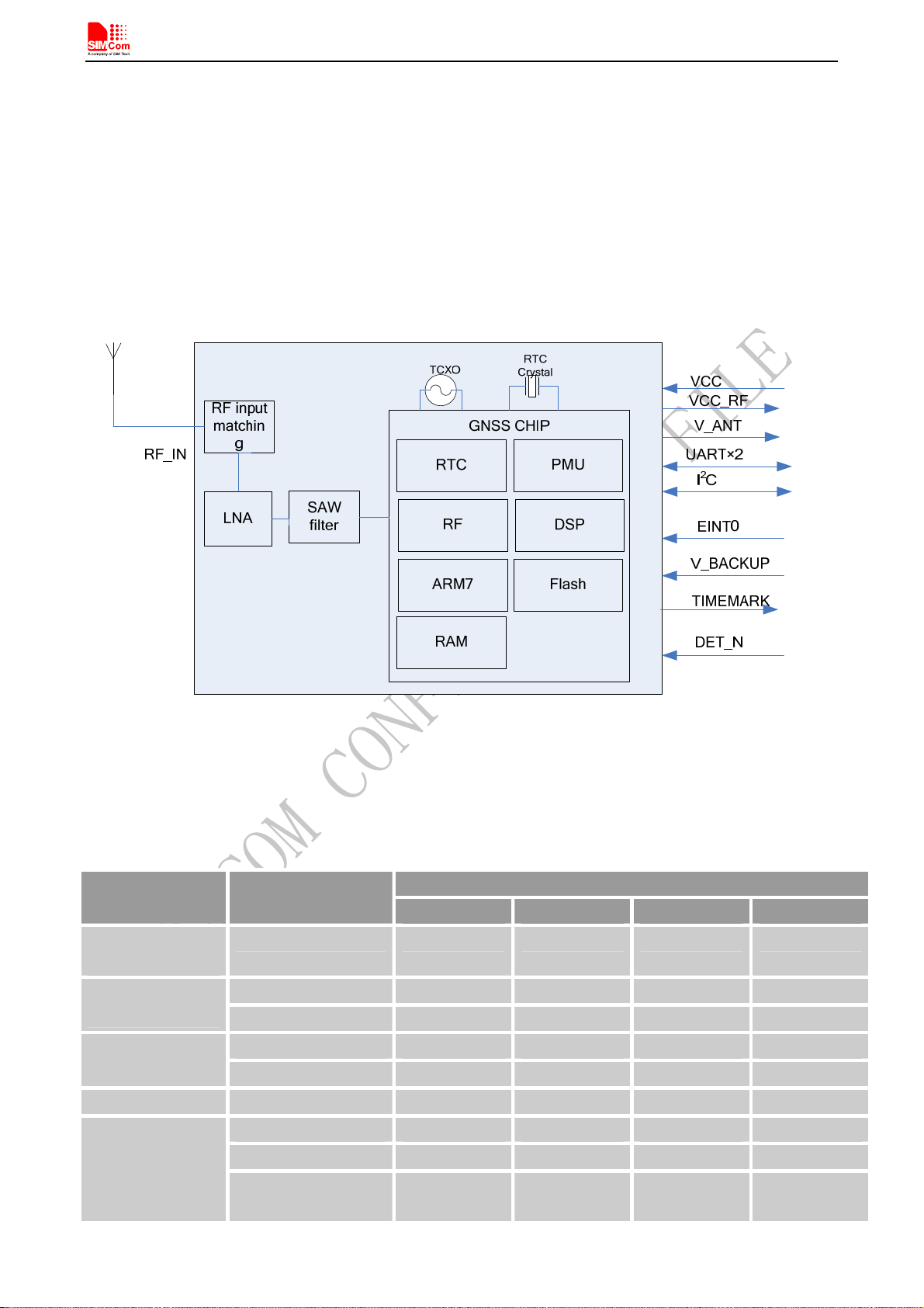
2.1 SIM68R Functional Diagram
The following figure shows a functional diagram of the SIM68R and illustrates the main functional parts:
z The GNSS chip
z SAW filter
z The antenna interface
z The communication interface
z The control signals
Figure 1: SIM68R functional diagram
2.2 GNSS Performance
Table 1: GNSS performance
Parameter Description
Min Type Max Unit
Horizontal Position
Accuracy
(1)
Autonomous <2.5 m
Without Aid 0.1 m/s Velocity
Accuracy(2)
Acceleration
Accuracy
DGPS 0.05 m/s
Without Aid 0.1
DGPS 0.05
Timing Accuracy 10
Dynamic
Performance
Maximum Altitude 18000
Maximum Velocity 515
Performance
m/s
m/s
nS
m
m/s
2
2
Maximum
4
G
Acceleration
SIM68R_Hardware Design_V1.02 9 2013-01-22
Page 10
Smart Machine Smart Decision
(3)
Time To First Fix
Hot start <1 s
Warm s t ar t 26 s
Cold start 28 s
A-GPS TTFF(EPO
in flash mode)
Sensitivity
Receiver
Power
consumption-A
(4)
Hot start 0.7 s
Warm s t ar t 1.5 s
Cold start 12.5 s
Autonomous
-148 dBm
acquisition(cold start)
Re-acquisition -160 dBm
Tracking -167 dBm
Channels 132
Update rate 1 10 Hz
Tracking L1, CA
Code
Protocol support
NMEA,PMTK
Acquisition 34 mA
Continuous tracking 30 mA
Sleep current <440 uA
Backup current 14 uA
(1) 50% 24hr static, -130dBm
(2) 50% at 30m/s
(3) –130 dBm, GPS&GLONASS mode
(4) Single Power supply 3.3V under GPS+GLONASS signal
2.3 General features
Table 2: General features
Parameters Value
Supply voltage VCC +2.8V~4.3V
Supply voltage ripple VCC 54 mV(RMS) max @ f = 0~3MHz
15 mV(RMS) max @ f > 3 MHz
Power consumption(acquisition) 37mA type. @ VCC=3.3 V
Power consumption(sleep) 440uA type. @ VCC=3.3 V
Storage temperature -40ºC~+85ºC
Operating temperature -40ºC~+85ºC (note 1)
I/O signal levels
VIL -0.3V~0.8V
VIH 2.0V~3.6V
VOL -0.3V~0.4V
VOH 2.4V~3.1V
I/O output sink/source capability +/- 3mA max
I/O input leakage +/- 10 uA max
SIM68R_Hardware Design_V1.02 10 2013-01-22
Page 11

Smart Machine Smart Decision
Host port UART,UART1
Other port I2C
Serial port protocol (UART) NMEA; 8 bits, no parity, 1 stop bit; 115200 baud (configurable)
TM output (1PPS) 1 pulse per second, synchronized at rising edge, pulse length 300ms
Note 1: Operation in the temperature range –40°C~ –30°C is allowed but Time-to-First-Fix performance and tracking sensitivity
may be degraded.
SIM68R_Hardware Design_V1.02 11 2013-01-22
Page 12
Smart Machine Smart Decision
3 Package Information
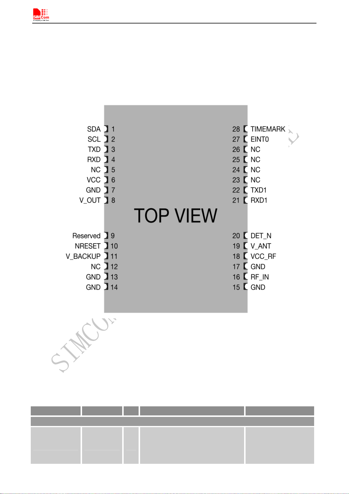
3.1 Pin out Diagram
Figure 2: SIM68R pin out diagram (Top view)
3.2 Pin Description
Table 3: Pin description
Pin name Pin number I/O Description Comment
Power supply
Main power input, which will be used
VCC 6 I
SIM68R_Hardware Design_V1.02 12 2013-01-22
to power the baseband and RF section
internally.
Provide clean and stable
power source to this pin.
Add a 4.7uF capacitor to
this pin for decoupling.
Page 13

Smart Machine Smart Decision
V_OUT 8 O
VCC_RF 18 O
V_ANT 19 I Antenna Bias voltage
V_BACKUP 11 I
Output voltage. It Has been connected
to VCC inside the Module
2.8V output power supply for active
antenna
The backup battery input power supply
for RTC
If unused, keep open.
If unused, keep open.
If unused , connect to
GND
If unused, keep open.
GND 7,13,14,15,17 Ground GND
Host port interface
SDA 1 I/O I2C data
If unused, keep open.
SCL 2 I/O I2C C Clock
TXD 3 O Serial output If unused, keep open
RXD 4 I Serial input If unused, keep open
TXD1 22 O Serial output as RTCM
RXD1 21 I Serial input as RTCM
GPIOs
This interrupt source could act as wake
EINT0 27 I
up event during power saving mode.
Provide an interrupt on either high or
low logic level or edge-sensitive
Not supported yet, keep
open.
interrupt
TIMEMARK 28 O
Time Mark outputs timing pulse related
to receiver time
If unused, keep open.
NRESET 10 I Reset input, active low If unused, keep open.
DET_N 20 I Active Antenna Detect If unused, keep open.
RF interface
RF_IN 16
I Radio antenna connection
Impendence must be
controlled to 50Ω.
Other interface
NC
5,12,23,24,25
,26
Not Connected
Reserved 9 Not Connected
SIM68R_Hardware Design_V1.02 13 2013-01-22
Page 14
Smart Machine Smart Decision
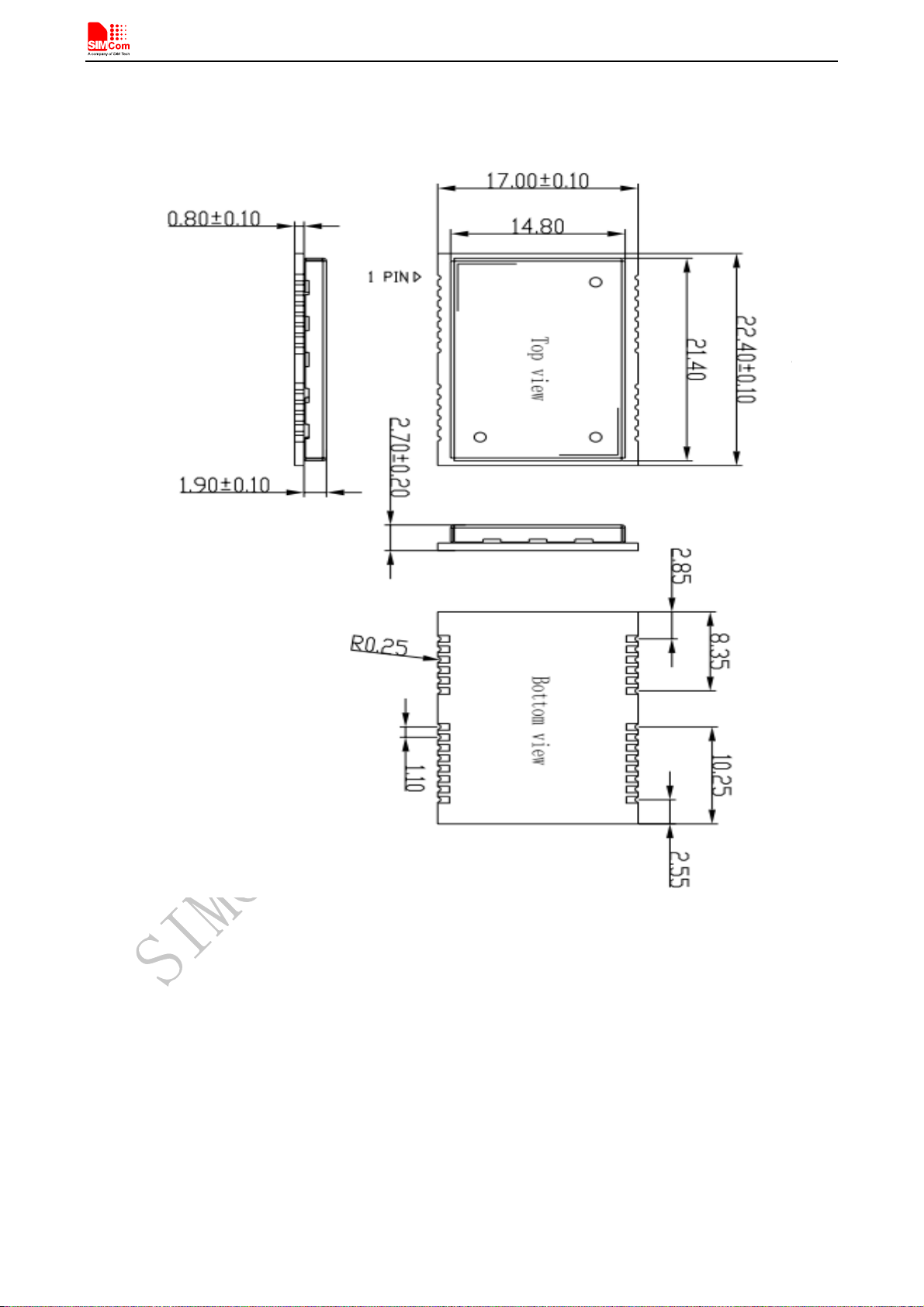
3.3 Package Dimensions
Following figure shows the Mechanical dimensions of SIM68R (top view, side view and bottom view).
Figure 3: SIM68R mechanical dimensions (Unit: mm)
SIM68R_Hardware Design_V1.02 14 2013-01-22
Page 15
Smart Machine Smart Decision
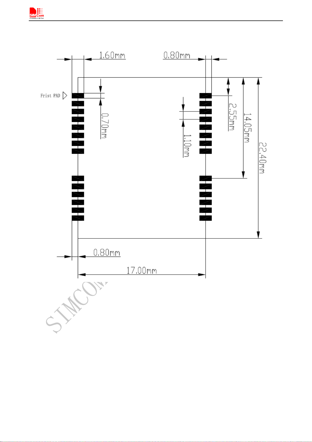
3.4 SIM68R Recommended PCB Decal
Figure 4: Recommended PCB decal (top view) (Unit: mm)
SIM68R_Hardware Design_V1.02 15 2013-01-22
Page 16

Smart Machine Smart Decision
4 Application Interface
4.1 Power Management
4.1.1 Power Input
The power supply range is from 2.8V to 4.3V, and it should be able to provide sufficient current up to 100mA.
4.1.2 Starting SIM68R
z When power is first applied, SIM68R goes into operation mode.
4.1.3 Verification of SIM68R Start
System activity indication depends upon the chosen serial interface:
z When it is activated, SIM68R will output messages at the selected UART speed, and message types.
Note: the baud rate information can be found on the label.
4.1.4 Power Saving Modes
SIM68R supports operating modes for reduced average power consumption like sleep mode, backup mode,
TM
periodic mode, and AlwayLocate
mode.
z Sleep mode: In this mode the receiver stays at full on power state. When this mode that can be wake up by
the host sends the command through the communication interface or external interrupt.
z Backup mode: In this mode the SIM68R must be supplied by the backup and it can help to count down the
time for backup mode. Software on host side to send the command through the communication interface
into the backup mode.
z Periodic mode: In this mode the SIM68R enters tracking and backup mode according to the interval
configured by users in the commands.
z AlwayLocate
TM
mode: AlwayLocate
TM
is an intelligent controller of SIM68R periodic mode. Depending on
the environment and motion conditions, SIM68R can adaptive adjust the on/off time to achieve balance of
positioning accuracy and power consumption.
Note: the modes mentioned above are operated by PMTK commands, users can refer to document [3] for more information.
SIM68R provides very low leakage battery back up memory, which contains all the necessary GNSS information
for quick start up and a small amount of user configuration variables. It needs a 3V power supply for V_BACKUP
pin, and the stable operation region ranges from very light load to about 3mA.
SIM68R_Hardware Design_V1.02 32 2013.01.22
Page 17

Smart Machine Smart Decision
4.1.5 Operating Mode
Table 4: Power supply and clock state according to operation mode
Mode VCC V_BACKUP Internal LDO Main clock RTC clock
Full on on on on on on
Sleep on on on off on
Backup on on off off on
4.1.5.1 Full on Mode
The module will enter full on mode after first power up with factory configuration settings. Power consumption
will vary depending on the amount of satellite acquisitions and numbers of satellites in track. This mode is also
referenced as Full on, Full Power or Navigation mode.
Navigation is available and any configuration settings are valid as long as the VCC power supply is active. When
the power supply is off, settings are reset to factory configuration and receiver performs a cold start on next power
up.
4.1.5.2 Sleep Mode
Sleep mode means a low quiescent (440uA type.) power state, non-volatile RTC, and backup RAM block is
powered on. Other internal blocks like digital baseband and RF are internally powered off. The power supply
input VCC shall be kept active all the time, even during sleep mode.
Entering into sleep mode is sent PMTK command through the communication interface by host side.
Waking up from sleep mode is sent any byte through the communication interface by host side.
4.1.6 VCC_RF
VCC_RF is a 2.8V output for external active antenna, if the external active antenna works at 2.8V voltage supply
domain, the user can use the VCC_RF directly. If the antenna’s power supply is not 2.8V, it should be open. For
passive antenna, VCC_RF should be open.
4.2 UART Interface
SIM68R includes two UART (UART and UART1) interface for serial communication. The UART is as NMEA
output and PMTK command input. The receiver (RXD) and transmitter (TXD) side of every port contains a
16-byte FIFO and has 256 bytes URAM. the baud rates are selectable and ranging from 4.8 to 921.6kbps through
CoreBuilder tool. UART can provide the developers signal or message outputs. UART1 is as RTCM input.
For details about CoreBuilder information, please refer to document [2]
SIM68R_Hardware Design_V1.02 17 2013-01-22
Page 18

Smart Machine Smart Decision
Table 5: Host port multiplexed function pins
Pin name Pin number UART function
TXD 3 data transmit
RXD 4 data receive
4.3 I
The SCL and SDA are the I
2
C interface
2
C bus pins, which can be connected to a external I2C interface EEPROM up to 1
Mbits for reading and writing data into EEPROM. This can be used to store configurations permanently.
NOTE: The EEPROM can’t be supported currently.
4.4 Timemark Output
The Timemark pin outputs pulse-per-second (1PPS) pulse signal for precise timing purposes. It will come out
after successfully positioning .The Timemark signal can be provided through designated output pin for many
external applications. This pulse is not only limited to be active every second but also allowed to set the required
duration, frequency, and active high/low by programming user-defined settings.
4.5 DET_N
DET_N is an input pin and is used to report whether an external circuit has detected an external antenna or
not .Low level means the antenna has been detected. High level means no external antenna has been detected.
NOTE: The High level for DET_N should be 2.85V CMOS level.
4.6 A-GPS
A-GPS is the meaning of Assisted GPS, which is a system that can under certain conditions improve the startup
performance, or time-to-first-fix (TTFF) of a GPS satellite-based positioning system. SIM68R module supports
EPO file, EASY mode and SBAS/RTCM
4.6.1
The SIM68R supports the EPO (Extended Prediction Orbit) data service. The EPO data service is supporting
7/14/30-day orbit predictions to customers. It needs occasional download from EPO server. Supply of aiding
information like ephemeris, almanac, rough last position and time and satellite status and an optional time
synchronization signal will reduce time to first fix significantly and improve the acquisition sensitivity.
The user should update the EPO files from the EPO server daily through the internet. Then the EPO data should
send to the SIM68R by the HOST side. SIM68R has the short cold TTFF and warm TTFF, when the A-GPS is
used.
Note: For more information about EPO, please contact SIMCom sales. users can refer to document [4] for more information
SIM68R_Hardware Design_V1.02 18 2013-01-22
EPO
Page 19

Smart Machine Smart Decision
4.6.2 EASY MODE
EASY is the abbreviation of Embedded Assist System, it works as embedded firmware which accelerates TTFF
by predicting satellite navigation messages from received ephemeris.
No additional computing interval for EASY task. EASY is efficiently scheduled and computed in free time of
every second after GPS navigation solution.
EASY function is conceptually designed to automatically engage for predicting after first receiving the broadcast
ephemeris. After a while (generally tens of seconds), 3-day extensions will be completely generated then all
EASY functions will be maintained at a sleep condition. EASY assistance is going to be engaged when the GPS
requests in new TTFF condition or re-generates again with another new received ephemeris. Meanwhile, TTFF
will be benefited by EASY assistance.
Note: EASY function is default open and can be closed by PMTK command.
4.6.3
SBAS and RTCM
SBAS is the abbreviation of Satellite Based Augmentation System. The SBAS concept is based on the
transmission of differential corrections and integrity messages for navigation satellites that are within sight of a
network of reference stations deployed across an entire continent. SBAS messages are broadcast via geostationary
satellites able to cover vast areas.
Several countries have implemented their own satellite-based augmentation system. Europe has the European
Geostationary Navigation Overlay Service (EGNOS) which covers Western Europe and beyond. The USA has
its Wide Area Augmentation System (WAAS). Japan is covered by its Multi-functional Satellite Augmentation
System (MSAS). India has launched its own SBAS program named GPS and GEO Augmented Navigation
(GAGAN) to cover the Indian subcontinent.
SIM68R module supports SBAS and RTCM, but only one mode can be applied at one time, and SBAS is the
default feature, customers who want to apply RTCM in the design can contact SIMCom sales for supporting
4.7 GNSS Antenna
The SIM68R is designed for use with passive and active antennas.
Table 6: Antenna Specifications
Parameter Specification
Passive and active antenna
Frequency range 1574~1606MHz
Active Antenna Recommendations
Polarization RHCP
Gain 20dB<Gain<30dB
Noise Figure <1.5 dB
SIM68R_Hardware Design_V1.02 19 2013-01-22
Page 20

Smart Machine Smart Decision
4.7.1 Antenna Interface
The SIM68R receives L1 band signals from GNSS and GALILEO satellites at a nominal frequency of 1574~
1606 MHz. The RF signal is connected to the RF_IN pin.
And the trace from RF_IN to antenna should be 50Ω
controlled.
To suit the physical design of individual applications the RF interface pad can lead to three alternatives:
z Recommended approach: solderable
RF coaxial cable assembly antenna connector, such as HRS’
U.FL-R-SMT(10) connector or I-PEX’s 20279-001E-01 RF connector.
z SMA connector.
4.7.2
GNSS Antenna Choice Consideration
To obtain excellent GNSS receiving performance, a good antenna will always be required. The antenna is the
most critical item for successful GNSS receiving in a weak signal environment. Proper choice and placement of
the antenna will ensure that satellites at all elevations can be seen, and therefore, accurate fix measurements are
obtained.
4.7.2.1 Passive Antenna
Passive antenna contains only the radiating element, e.g. the ceramic patch, the helix structure, and chip
antennas. Sometimes they also contain a passive matching network to match the electrical connection to 50 Ohms
impedance.
The most common antenna type for GNSS applications is the patch antenna. Patch antennas are flat, generally hav
e a ceramic and metal body and are mounted on a metal base plate.
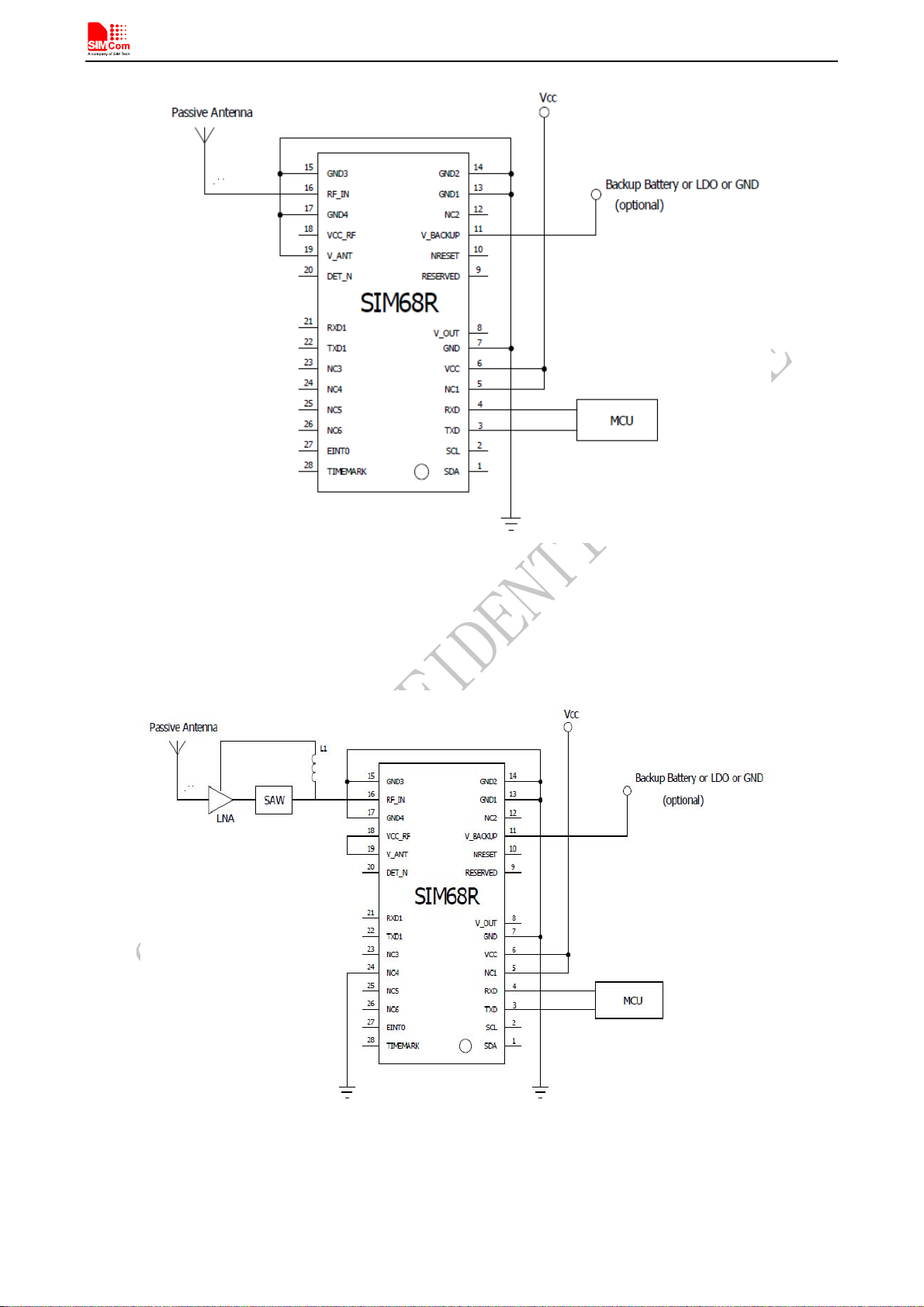
Figure 5 shows a minimal setup for a PVT GNSS receiver with SIM68R module.
SIM68R_Hardware Design_V1.02 20 2013-01-22
Page 21
Smart Machine Smart Decision
Figure 5: SIM68R passive antenna design
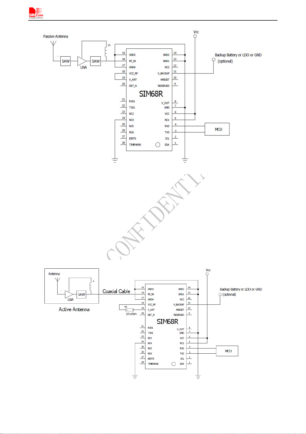
For best performance with passive antenna designs user can use an external LNA to increase the sensitivity up
3~4 dB. Please see Figure 6 and Figure 7.
Figure 6: SIM68R passive antenna design (with external LNA and SAW)
SIM68R_Hardware Design_V1.02 21 2013-01-22
Page 22
Smart Machine Smart Decision
Figure 7: SIM68R passive antenna design for best performance
4.7.2.2 Active Antennas
Active antennas have an integrated Low-Noise Amplifier (LNA). They can be directly connected to RF_IN. If an
active antenna is connected to RF_IN, the LNA of the antenna needs to be supplied with the correct voltage
through pin V_ANT. Usually, the supply voltage is fed to the antenna through the coaxial RF cable shown as
Figure 8. The output voltage of PIN 18 is 2.8V. If the supply voltage of active antenna is 2.8V, VCC_RF can
supply the voltage through the pin V_ANT.
Figure 8: SIM68R Active antenna design
SIM68R_Hardware Design_V1.02 22 2013-01-22
Page 23
Smart Machine Smart Decision
If the customer’s design is for automotive applications, then an active antenna can be used and located on top of
the car in order to guarantee the best signal quality.
GNSS antenna choice should base on the designing product and other conditions. For detailed Antenna designing
consideration, please refer to related antenna vendor’s design recommendation. The antenna vendor will offer
further technical support and tune their antenna characteristic to achieve successful GNSS reception performance
depending on the customer’s design.
4.7.2.3 Active antenna bias power
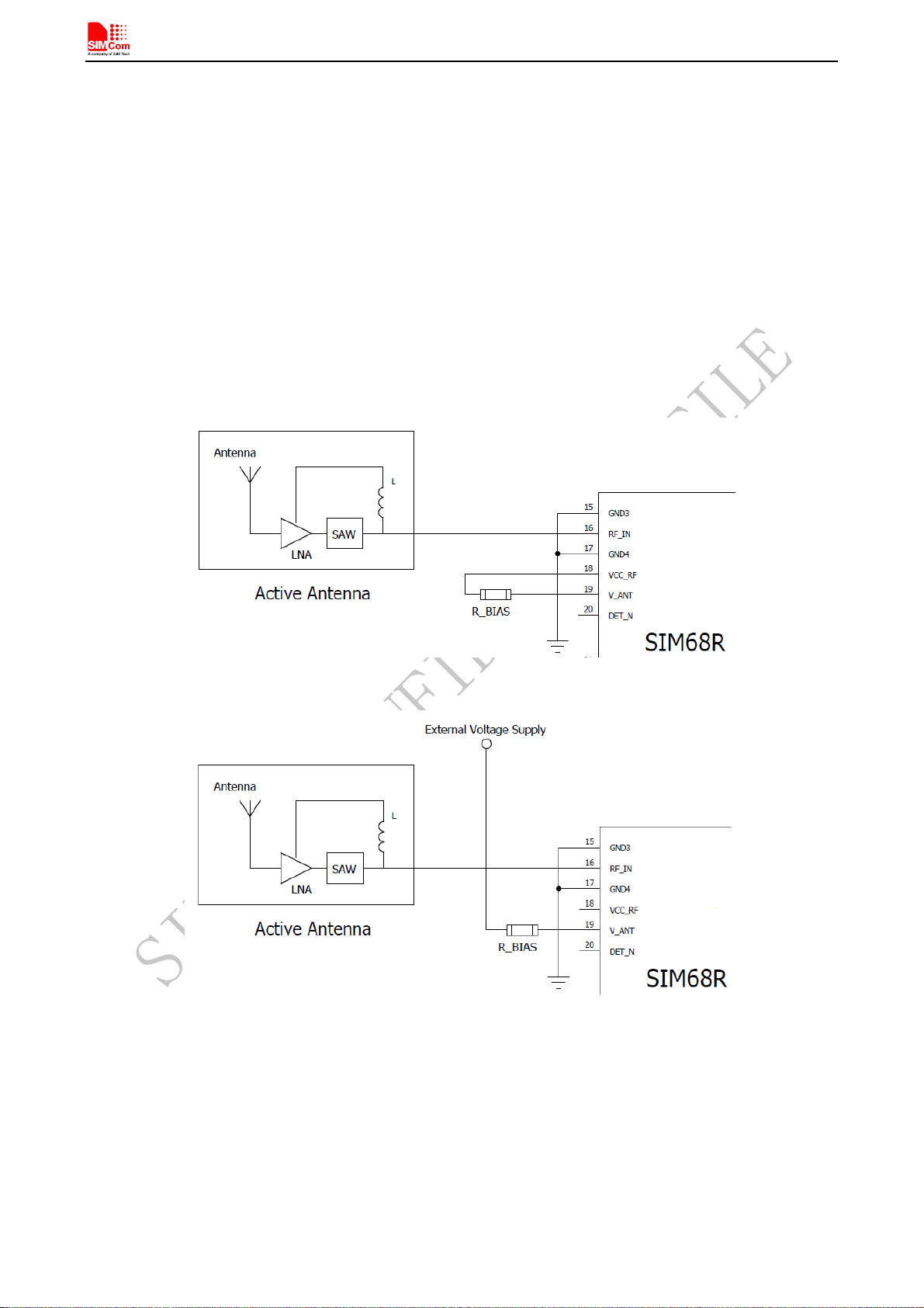
There are two ways to supply the bias voltage to pin V_ANT. For internal supply, the VCC_RF output must be
connected to V_ANT to supply the antenna with a filtered supply voltage. However, the voltage specification of
the antenna has to match the actual supply voltage of the SIM68R Receiver. For External supply, the supply
should be virtually free of noise.
Figure 9: Internal supply Antenna bias voltage
Figure 10: External supply Antenna bias voltage
4.7.3 Active antenna supervisor
SIM68R Technology provides the means to implement an active antenna supervisor with a minimal number of
parts. The antenna supervisor is highly configurable to suit various different applications.
Note: The standard firmware does not support active antenna supervisor.
SIM68R_Hardware Design_V1.02 23 2013-01-22
Page 24
Smart Machine Smart Decision
4.7.3.1 Short circuit Detection
If a short circuit in the active antenna pulls V_ANT to ground, then the module will detect it, and the module will
report $GPTXT,01,01,02,ANTSTATUS=SHORT*6D sentence through the serial port. The customer should
check short circuit.
NOTE: The antenna supply voltage is not derived from VCC_RF.
4.7.3.2 Open circuit Detection
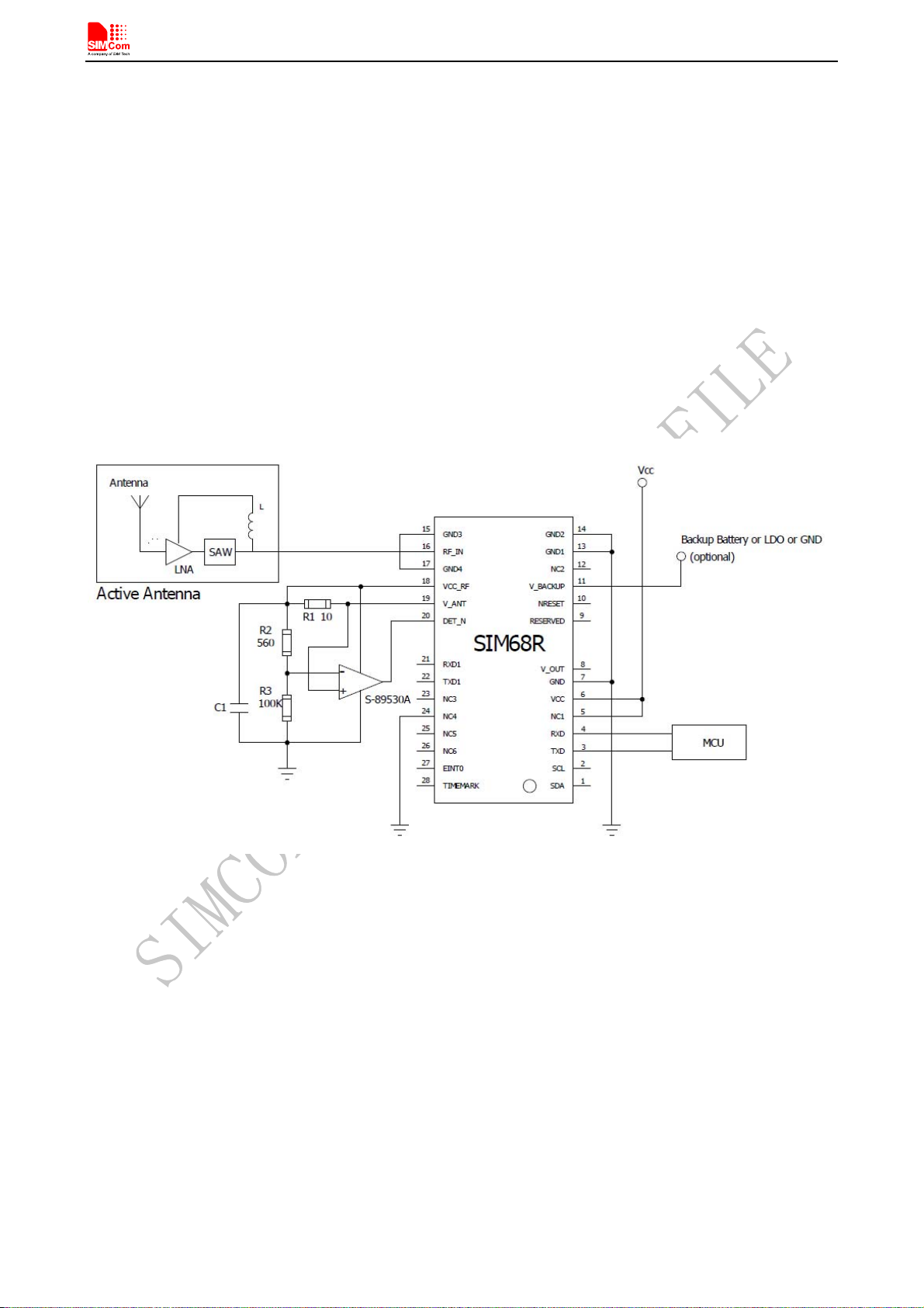
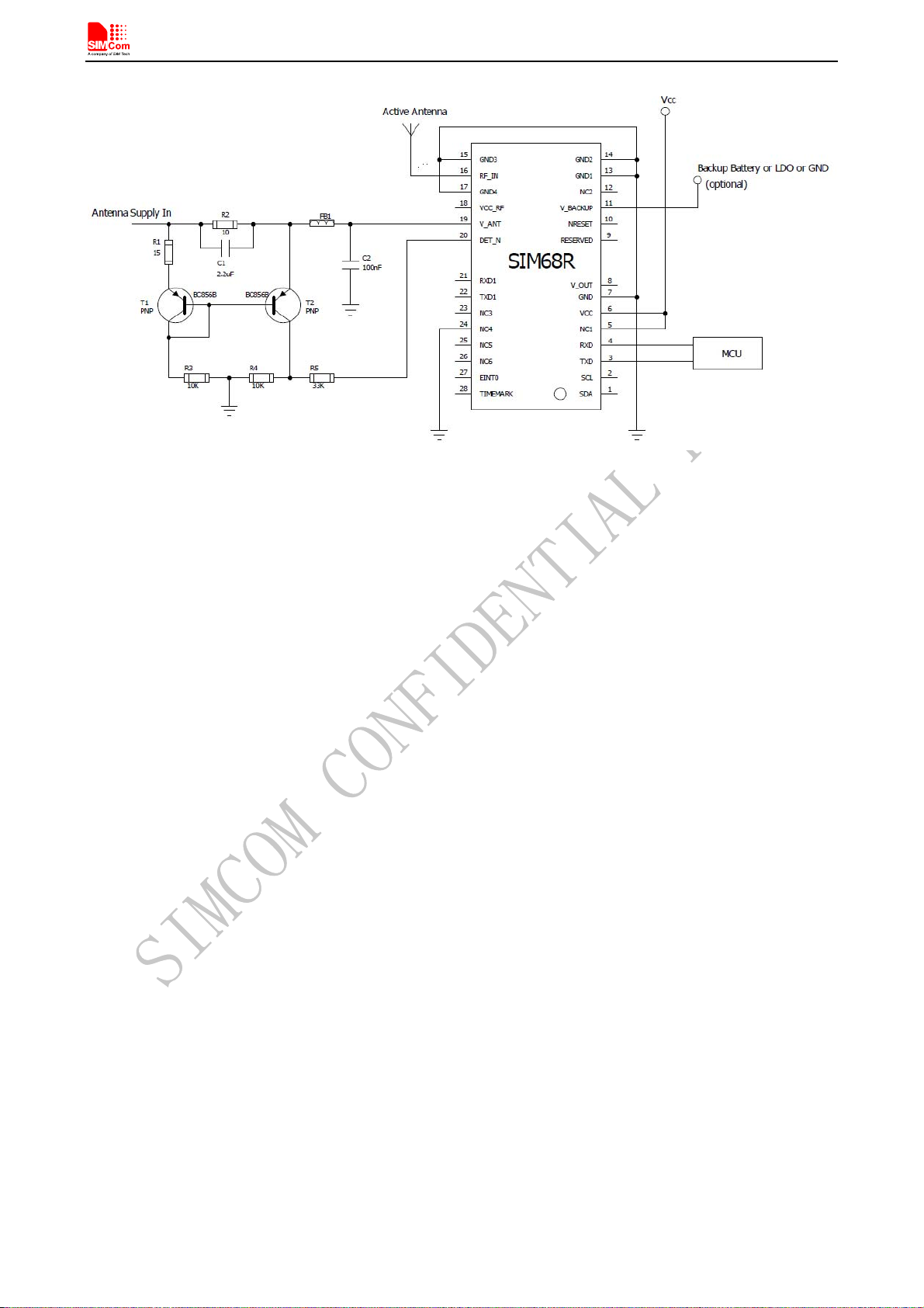
Firmware supports an active antenna supervisor circuit, which is connected to the pin DET_N. An example of an
open circuit detection circuit is shown in Figure 11and Figure 12. High (2.85V level) on DET_N means that an
external antenna is not connected, and the module will report $GPTXT,01,01,02,ANTSTATUS=OPEN*2B
sentence through the serial port. Low on DET_N means that an external antenna is connected, and the module
will report $GPTXT,01,01,02,ANTSTATUS=OK*3B sentence through the serial port.
Figure 11: Open circuir detection-A
SIM68R_Hardware Design_V1.02 24 2013-01-22
Page 25
Smart Machine Smart Decision
Figure 12: Open circuir detection-B
If the antenna supply voltage is not derived from VCC_RF, do not exceed the maximum voltage rating of
DET_N.(5V)
SIM68R_Hardware Design_V1.02 25 2013-01-22
Page 26
Smart Machine Smart Decision
5 Electrical, Reliability and Radio Characteristics
5.1 Absolute Maximum Ratings
The absolute maximum ratings stated in Table 7 are stress ratings under non-operating conditions. Stresses
beyond any of these limits will cause permanent damage to SIM68R.
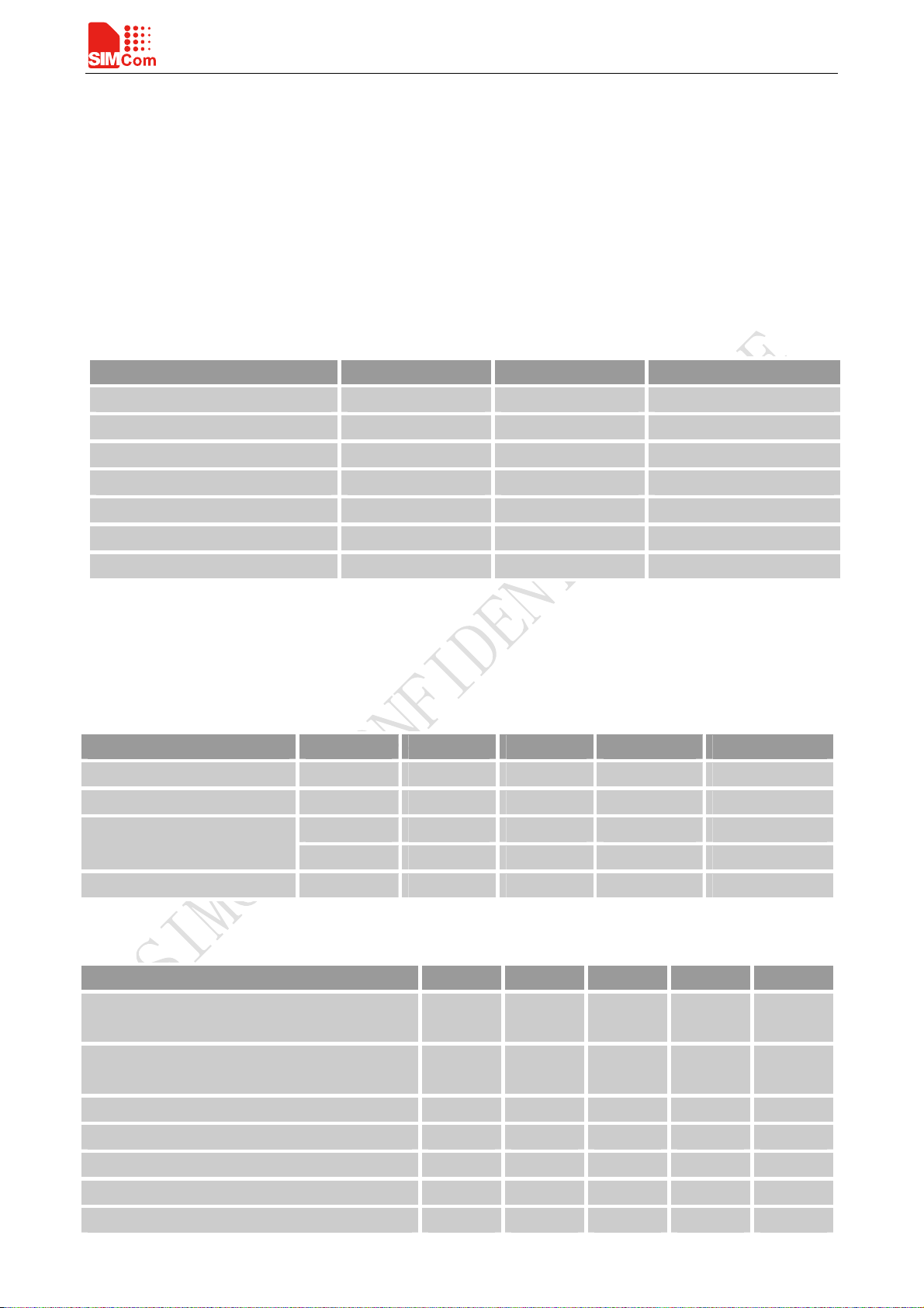
Table 7: Absolute maximum ratings
Parameter Min Max Unit
VCC - 4.3 V
V_ANT -5.5V +5.5 V
RF_IN - 3.08 V
V_BACKUP - 4.6 V
I/O pin voltage - 3.6 V
Storage temperature -45 +125 ℃
Operating Temperature -40 +85 ℃
5.2 Recommended Operating Conditions
Table 8: SIM68R operating conditions
Parameter Symbol Min Typ Max Unit
Operating temperature range -40 +25 +85 ℃
Main supply voltage VCC 2.8 3 4.3 V
VCC_RF 2.7 2.8 2.9 V Active antenna supply voltage
output
Backup battery voltage V_BACKUP 2.3 3.6 V
Table 9: SIM68R standard IO features
Parameter Symbol Min Typ Max Unit
Imax 20 mA
Low level output voltage
Test conditions IOL = 2mA and 4.0mA
High level output voltage
Test conditions IOL = 2mA and 4.0mA
Low level input voltage Vil -0.3 0.8 V
High level input voltage Vih 2.0 3.6 V
Input Pull-up resistance RPU 40 190 KΩ
Input Pull-dowm resistance RPD 40 190 KΩ
Input capacitance Cin 5 pF
SIM68R_Hardware Design_V1.02 32 2013.01.22
Vol
Voh
-0.3 0.40 V
2.4 3.1 V
Page 27
Smart Machine Smart Decision
Load capacitance C
8 pF
load
Tri-state leakage current IOZ -10 10 uA
5.3 Electro-Static Discharge
The GNSS engine is not protected against Electrostatic Discharge (ESD) in general. Therefore, it is subject to
ESD handing precautions that typically apply to ESD sensitive components. Proper ESD handing and packaging
procedures must be applied throughout the processing, handing and operation of any application using a SIM68R
module.
The measured values of SIM68R are shown as the following table:
Table 10: The ESD endure statue measured table (Temperature: 25 , Humidity:45% )℃
Part Contact discharge Air discharge
VCC ±5KV ±10KV
V_BACKUP ±5KV ±6KV
GND ±5KV ±10KV
RXD, TXD ±4KV ±8KV
RF_IN ±5KV ±10KV
NRESET ±4KV ±8KV
5.4 Certification
SIM68R meets the requirements of Directive 2002/95/EC of the European Parliament and of the Council on the
Restriction of Hazardous Substance (RoHS).and has acquired CE certification.
SIM68R_Hardware Design_V1.02 27 2013-01-22
Page 28
Smart Machine Smart Decision
6 Manufacturing
6.1 Top and Bottom View of SIM68R
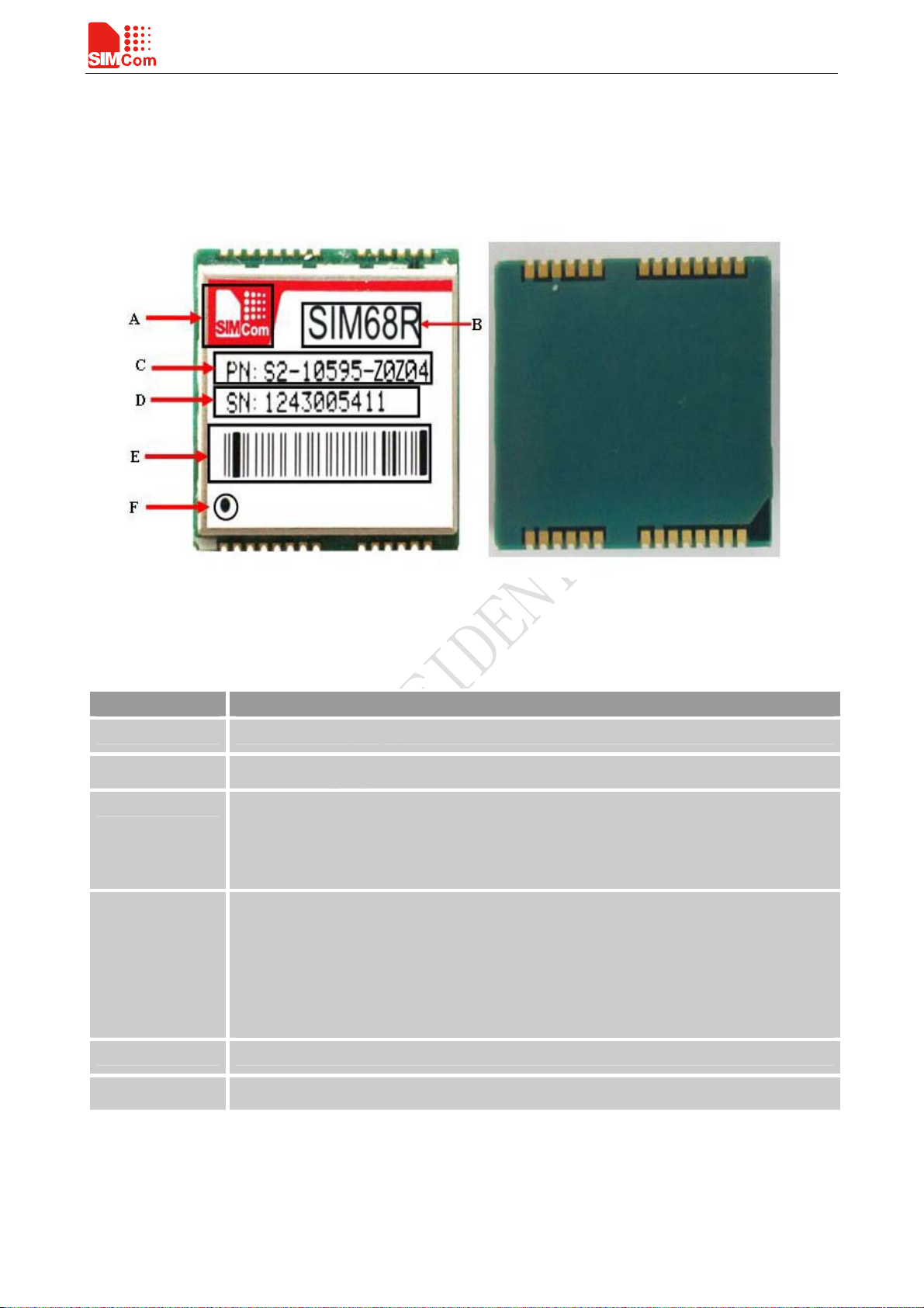
Figure 13: Top and bottom view of SIM68R
Table 11: Illustration of module information
Item Description
A LOGO
B Module name
C Module part number
Hardware number and software number included;
ex.S2-10595 is hardware number
Z0Z04 is software number
D Module serial number
The first number stands for factory code;
The second number stands for year code;
The third to eighth numbers is the SN number in hexadecimal numeric;
The last two numbers stands for MNEA sentence baud rate, “11” stands for 115200, “96”
stands for 9600;
E Module bar code
F PIN 1 Mark
6.2 Assembly and Soldering
The SIM68R module is intended for SMT assembly and soldering in a Pb-free reflow process on the top side of
the PCB. Suggested solder paste stencil height is 150um minimum to ensure sufficient solder volume. If required
SIM68R_Hardware Design_V1.02 32 2013.01.22
Page 29
Smart Machine Smart Decision
paste mask pad openings can be increased to ensure proper soldering and solder wetting over pads.
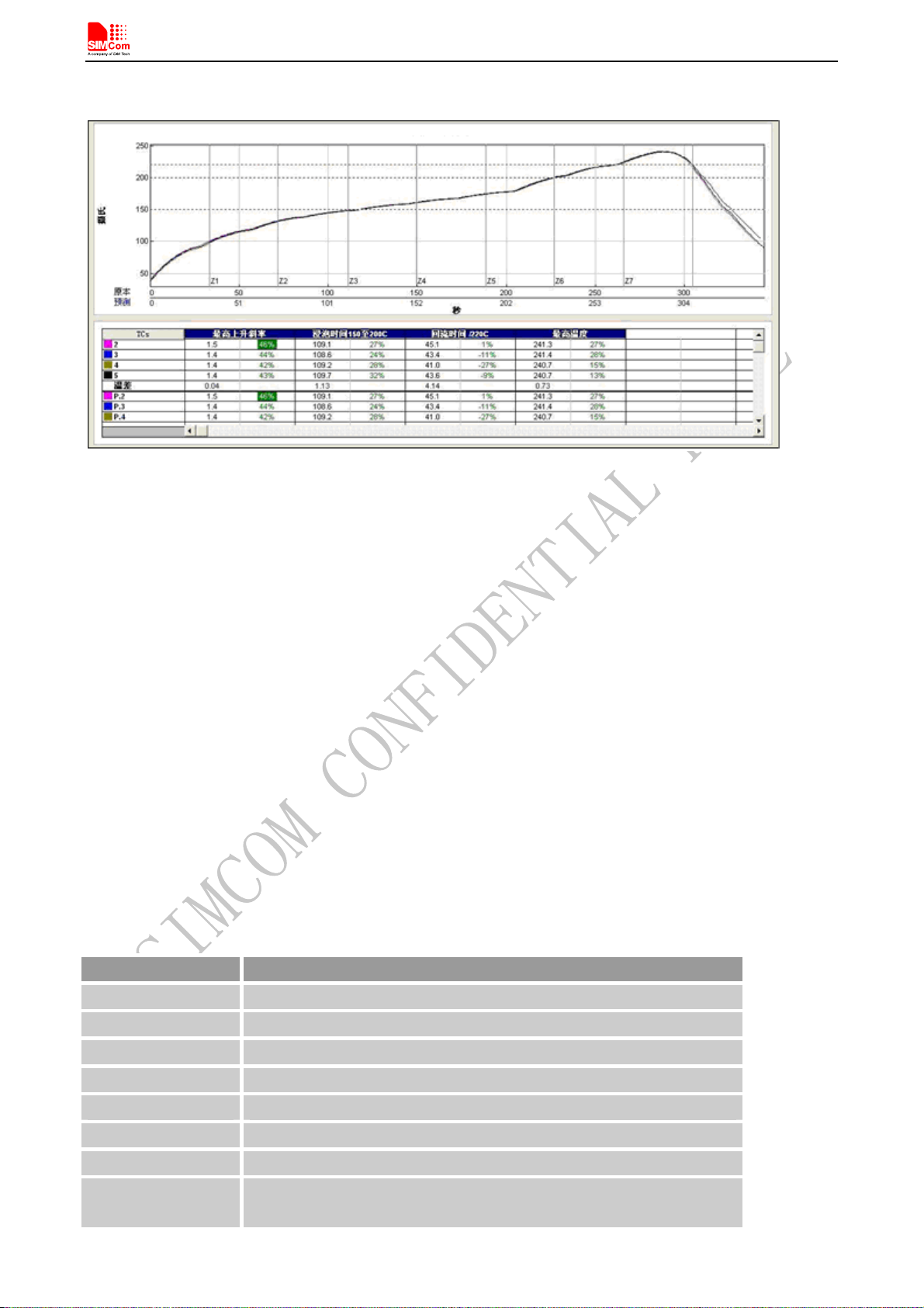
The following figure is the Ramp-Soak-Spike Reflow Profile of SIM68R:
Figure 14: The Ramp-Soak-Spike reflow profile of SIM68R
SIM68R is Moisture Sensitive Devices (MSD), appropriate MSD handling instruction and precautions are
summarized in Chapter 6.3.
SIM68R modules are also Electrostatic Sensitive Devices (ESD), handling SIM68R modules without proper ESD
protection may destroy or damage them permanently.
Avoid ultrasonic exposure due to internal crystal and SAW components.
6.3 Moisture sensitivity
SIM68R module is moisture sensitive at MSL level 3, dry packed according to IPC/JEDEC specification
J-STD-020C. The calculated shelf life for dry packed SMD packages is a minimum of 12 months from the bag
seal date, when stored in a non condensing atmospheric environment of <40°C/90% RH.
Table 10 lists floor life for different MSL levels in the IPC/JDEC specification:
Table 12: Moisture Classification Level and Floor Life
Level Floor Life(out of bag)at factory ambient≦+30 /60%RH or as stated℃
1 Unlimited at ≦+30 /85% RH℃
2 1 year
2a 4 weeks
3 168 hours
4 72 hours
5 48 hours
5a 24 hours
6 Mandatory bake before use. After bake, module must be reflowed within
the time limit specified on the label.
SIM68R_Hardware Design_V1.02 29 2013-01-22
Page 30

Smart Machine Smart Decision
Factory floor life is 1 week for MSL 3, SIM68R must be processed and soldered within the time. If this time is
exceeded, or the humidity indicator card in the sealed package indicates that they have been exposed to moisture,
the devices need to be pre-baked before the reflow solder process.
Both encapsulate and substrate materials absorb moisture. IPC/JEDEC specification J-STD-020 must be observed
to prevent cracking and delamination associated with the "popcorn" effect during reflow soldering. The popcorn
effect can be described as miniature explosions of evaporating moisture. Baking before processing is required in
the following cases:
z Humidity indicator card: At least one circular indicator is no longer blue
z Floor life or environmental requirements after opening the seal have been exceeded, e.g. exposure to
excessive seasonal humidity.
Refer to Section 4 of IPC/JEDEC J-STD-033 for recommended baking procedures.
Notes: Oxidation Risk: Baking SMD packages may cause oxidation and/or inter metallic growth of the terminations, which if
excessive can result in solder ability problems during board assembly. The temperature and time for baking SMD packages are
therefore limited by solder ability considerations. The cumulative bake time at a temperature greater than 90°C and up to 125°C
shall not exceed 96 hours.
6.4 ESD handling precautions
SIM68R modules are Electrostatic Sensitive Devices (ESD). Observe precautions for handling!
Failure to observe these precautions can result in severe damage to the GNSS receiver!
GNSS receivers are Electrostatic Sensitive Devices (ESD) and require special precautions when handling.
Particular care must be exercised when handling patch antennas, due to the risk of electrostatic charges. In
addition to standard ESD safety practices, the following measures should be taken into account whenever
handling the receiver:
Unless there is a galvanic coupling between the local GND (i.e. the work Table) and the PCB GND, then the first
point of contact when handling the PCB shall always be between the local GND and PCB GND.
Before mounting an antenna patch, connect ground of the device
When handling the RF pin, do not come into contact with any charged capacitors and be careful when contacting
materials that can develop charges (e.g. patch antenna ~10pF, coax cable ~50-80pF/m, soldering iron, …)
To prevent electrostatic discharge through the RF input, do not touch the mounted patch antenna.
When soldering RF connectors and patch antennas to the receiver’s RF pin, the user must make sure to use an
ESD safe soldering iron (tip).
6.5 Shipment
SIM68R is designed and packaged to be processed in an automatic assembly line, and it is now packaged in
SIM68R tray.
SIM68R_Hardware Design_V1.02 30 2013-01-22
Page 31
Smart Machine Smart Decision
7 Reference Design
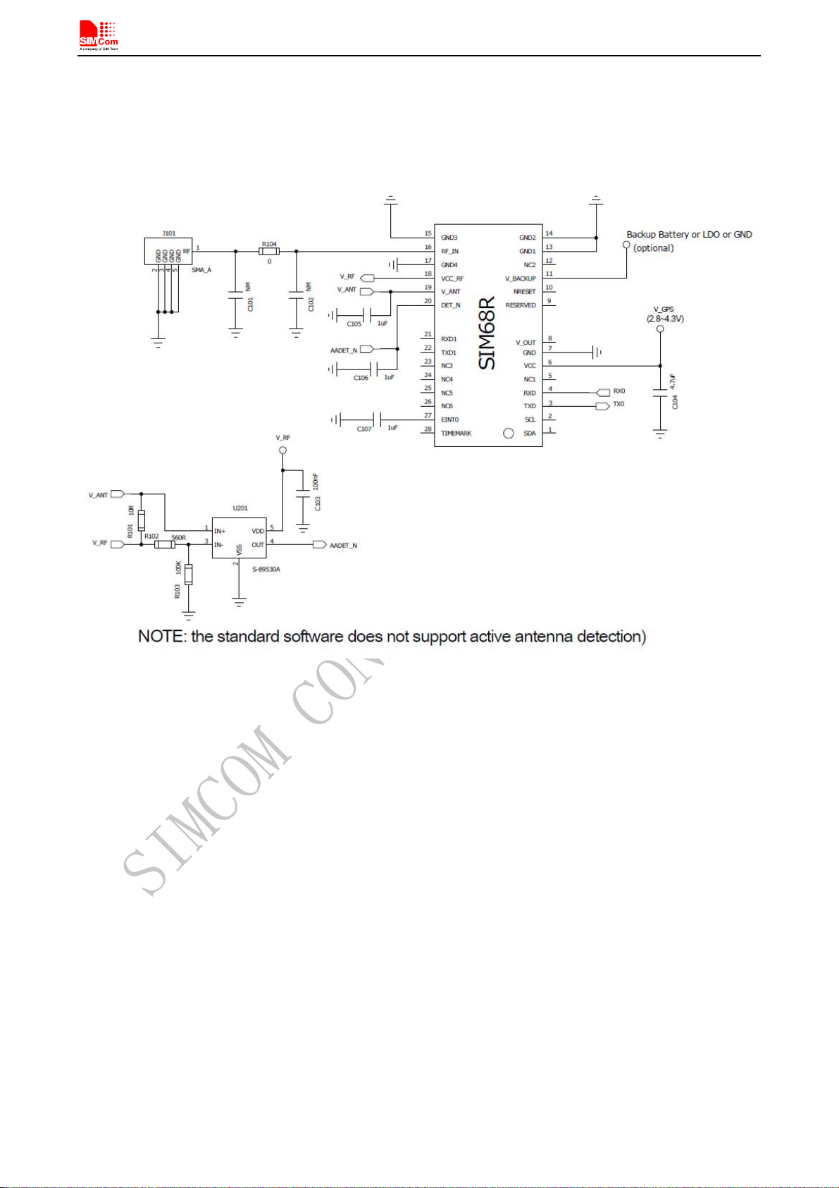
Figure 15: Example application schematic with UART
Notes:
1) The pin VCC_RF provides a 2.8V output level for external active antenna.
For active antenna, if antenna’s power domain is 2.8V, the pin VCC_RF could supply the voltage .Do not connect VCC_RF
pin to RF_IN pin directly, use V_ANT pin to supply power. Connect VCC_RF pin to V_ANT pin with 10ohm. If the
antenna’s power is not 2.8v, keep the pin VCC_RF open.
For passive antenna, the pin VCC_RF should be kept open, the pin V_ANT should be connected to GND.
SIM68R_Hardware Design_V1.02 31 2013-01-22
Page 32
Smart Machine Smart Decision
Appendix
A. Related Documents
Table 13: Related documents
SN Document name Remark
[1] MT3333_data_sheet_external_V1.01 MT3333 datasheet
[2] CoreBuilder_User_Manual_0_4 CoreBuilder User Manual
SIM28/68R/68V NMEA Messages
[3]
SpecificationV1.00
[4] EPO-II_Format_Protocol_Customer EPO-II_Format and Protocol
B. Terms and Abbreviations
Table 14: Terms and abbreviations
Abbreviation Description
A-GPS
CMOS Complementary Metal Oxide Semiconductor
EEPROM Electrically Erasable Programmable Read Only Memory
EPO Extended Prediction Orbit
ESD Electrostatic Sensitive Devices
GPS Global Positioning System
GLONASS Global Navigation Satellite System
GNSS Global Navigation Satellite System
I/O Input/Output
IC Integrated Circuit
Inorm Normal Current
Imax Maximum Load Current
Assisted Global Positioning System
kbps Kilo bits per second
RTCM Radio Technical Commission for Maritime services
MSL moisture sensitive level
NMEA National Marine Electronics Association
SBAS Satellite Based Augmentation Systems
QZSS Quasi-Zenith Satellites System
CEP Circular Error Probable
SGAGAN The GPS Aided Geo Augmented Navigation
SIM68R_Hardware Design_V1.02 32 2013.01.22
Page 33

Smart Machine Smart Decision
WAAS Wide Area Augmentation System
MSAS Multi-Functional Satellite Augmentation System
EASY Embedded Assist System
DGPS Difference Global Positioning System
SIM68R_Hardware Design_V1.02 33 2013-01-22
Page 34

Smart Machine Smart Decision
Contact us:
Shanghai SIMCom Wireless Solutions Ltd.
Add: SIM Technology Building,No.633,Jinzhong Road,Changning District,Shanghai P.R. China
200335
Tel: +86 21 3235 3300
Fax: +86 21 3235 3301
URL: www.sim.com/wm
SIM68R_Hardware Design_V1.02 34 2013-01-22
 Loading...