


SIMATIC NET
SPC4 Siemens PROFIBUS Controller
User Description Date 08.05.96
Order No. 6GK1 971-5XA00-0BA0


SINEC
(Siemens PROFIBUS Controller)
SPC4
User Description
Release: V1.2
Date: 08.05.1996

WKF B1 T2 SPC4
Liability Exclusion
We have tested the contents of this document regarding agreement
with the hardware and software described. Nevertheless, deviations
can’t be excluded and we can’t guarantee complete agreement. The
data in the document is checked regularly, however. Required
corrections are included in subsequent versions. We gratefully accept
suggestions for improvement.
Copyright
Copyright © Siemens AG 1995 All Rights Reserved
Unless permission has been expressly granted, passing on this
document or copying it, or using and sharing its content is not allowed.
Offenders will be held liable. All rights reserved, in the event a patent
is granted, or a utility model or design is registered.
The trademarks SIMATIC, SINEC and SOFTNET, L2 are protected
by law through registration by Siemens.
All other product- and system names are (registered) trademarks of
their respective owner and are to be treated as such.
Subject to technical change.
Page 2 Release V1.2 SPC4 User Description
Order Nr. 6GK1 971-5XA00-0BA0 Copyright (C) Siemens AG 1997. All rights reserved.

SPC4 WKF B1 T2
Table of Contens
1 INTRODUCTION 7
2 FUNCTION OVERVIEW 8
3 PIN ASSIGNMENT 9
4 MEMORY ASSIGNMENT 10
4.1 Addressing of the SPC4 10
4.2 Memory Area Distribution of the Internal RAM 11
4.2.1 Overview 11
4.2.2 RAM Parameter Block 12
4.2.3 SAP List 12
4.2.4 Data Areas in the Internal RAM 14
4.2.5 Addressing via the Memory Window 14
4.3 Assignment of the Parameter Latches 15
5 FLC INTERFACE 18
5.1 SAP List 18
5.1.1 Structure of the SAP List 18
5.1.2 Control Byte 18
5.1.3 Request SA 20
5.1.4 Request SSAP 20
5.1.5 Access Byte 20
5.1.6 Reply Update Ptr/ SDN-DDB-TIn-Tab-Ptr 21
5.1.7 Special Features for the DEFAULT SAP 22
5.2 SM-SAP List 22
5.3 Indication Queue 23
5.3.1 Description 23
5.3.2 Structure of the Indication Block 24
5.4 Reply on Indication Blocks 27
5.4.1 Function 27
5.4.2 Structure of the Reply-on-Indication Blocks 27
6 DP INTERFACE 29
6.1 Description 29
6.2 Productive Services 30
6.2.1 Data Exchange 30
6.2.2 Read Input Data 31
6.2.3 Read Output Data 32
6.2.4 Global Control (Sync, Freeze, Clear Data) 32
6.2.5 Leave Master 34
6.2.6 Baudrate Search 34
SPC4 User Description Release V1.2 Page 3
Copyright (C) Siemens AG 1997. All rights reserved. Order Nr. 6GK1 971-5XA00-0BA0

WKF B1 T2 SPC4
7 ASIC INTERFACE 36
7.1 Latch Parameters 36
7.1.1 Slot Time Register 36
7.1.2 Baudrate Register 36
7.1.3 BEGIN PTR Register 37
7.1.4 UMBR PTR Register 38
7.1.5 BASE PTR Register 38
7.1.6 TRDY Register 38
7.1.7 PREAMBLE Register 39
7.1.8 SYN Time Register 39
7.1.9 Delay Timer Register 39
7.1.10 Factor Delay Timer Clock Register 40
7.1.11 Mode Register 40
7.2 RAM Parameter Block 46
7.2.1 Indication Write Pointer 46
7.2.2 Indication Write PRE Pointer 46
7.2.3 Indication Read Pointer 46
7.3 Interrupt Controller 47
7.4 SPC4 Timer 52
7.4.1 Delay Timer 52
7.4.2 Idle Timer 53
7.4.3 Syni Timer 53
7.4.4 Slot Timer 53
7.4.5 Time Out Timer 54
8 ASYNCHRONOUS INTERFACE 55
8.1 Baudrate Generator 55
8.2 Transmitter 55
8.3 Receiver 55
8.4 Serial Bus Interface PROFIBUS Interface (asynchronous) 55
8.4.1 Interface Signals 55
8.4.2 Timing RS 485: 56
8.4.3 Example for the RS 232 Interface 57
9 SYNCHRONOUS INTERFACE 58
9.1 Overview 58
9.2 Baudrate Generator 58
9.3 Transmitter 58
9.4 Receiver 60
10 CLOCK SUPPLY 61
Page 4 Release V1.2 SPC4 User Description
Order Nr. 6GK1 971-5XA00-0BA0 Copyright (C) Siemens AG 1997. All rights reserved.

SPC4 WKF B1 T2
11 PROCESSOR BUS INTERFACE 63
11.1 Universal Processor Interface 63
11.2 Bus Interface Unit (BIU) 65
11.3 Dual Port RAM Controller 65
11.3.1 Function 65
11.3.2 Access to the SPC4 under LOCK 65
11.4 Other Pins 66
11.4.1 Test Pins 66
11.4.2 XHOLDTOKEN 66
11.4.3 XINTCI 66
11.5 Interrupt Timing 67
11.6 Reset Timing 67
11.7 Intel / Siemens 8051 (synchronous) etc. 68
11.7.1 Diagram 68
11.7.2 Timing 80C32 69
11.8 Intel X86 (asynchronous) 70
11.8.1 Diagram 70
11.8.2 Timing X86 71
11.9 Siemens 80C165 (asynchronous) 73
11.9.1 Diagram 73
11.9.2 Timing 80C165 74
11.10 Motorola 68HC16 (asynchronous) 76
11.10.1 Diagram 76
11.10.2 Timing 68HC16 76
11.11 Motorola 68HC11 (synchronous) 78
11.11.1 Diagram 78
11.11.2 Timing 68HC11 78
12 TECHNCIAL SPECIFICATION 80
12.1 Maximum Limits 80
12.2 Permissible Operating Values 80
12.3 DC Specification of the Pad Cells 81
12.4 Identification Data for the Output Drivers 81
13 CASING 82
13.1 Notes on Processing 83
14 BIBLIOGRAPHY 84
SPC4 User Description Release V1.2 Page 5
Copyright (C) Siemens AG 1997. All rights reserved. Order Nr. 6GK1 971-5XA00-0BA0

WKF B1 T2 SPC4
15 ADDRESS LIST 84
15.1 PNO 84
15.2 Technical Contact Persons in the Interface Center 84
16 APPENDIX 85
16.1 Server Software for the SPC4 85
16.1.1 Application 85
16.1.2 Special features of the PROFIBUS -PA / -FMS / -DP server software: 85
16.1.3 Functions of the Server Software 86
16.2 SIM1 88
16.2.1 Area of Appliction 88
16.2.2 Special Functions 89
16.2.3 Fields of application 89
16.2.4 Function of the Application 90
16.2.5 Electrical Data 91
Page 6 Release V1.2 SPC4 User Description
Order Nr. 6GK1 971-5XA00-0BA0 Copyright (C) Siemens AG 1997. All rights reserved.

SPC4 WKF B1 T2
1 Introduction
For simple and fast digital exchange between programmable logic controllers, Siemens offers its users
several ASICs. These ASICs are based on and are completely handled on the principles of the PROFIBUS
DIN 19245, Part 1 and the Draft, Part 3, of data traffic between individual programmable logic controller
stations.
The following ASICs are available to support intelligent slave solutions, that is, implementations with a
microprocessor.
The SPC (Siemens Profibus Controller) is built directly on Layer 1 of the OSI model and requires an
additional microprocessor for implementing Layers 2 and 7.
The ASPC2 already has integrated many parts of Layer 2, but the ASPC2 also requires a processor’s
support. This ASIC supports baud rates up to 12 Mbaud. In its complexity, this ASIC is conceived primarily
for master applications.
Due to the integration of the complete PROFIBUS-DP protocol, the SPC3 decisively relieves the processor
of an intelligent PROFIBUS slave. The SPC3 can be operated on the bus with a baud rate of up to 12
MBaud.
However, there are also simple devices in the automation engineering area, such as switches and
thermoelements, that do not require a microprocessor to record their states.
There are two additional ASICs available with the designations SPM2 (Siemens Profibus Multiplexer,
Version 2 ) and LSPM2 (Lean Siemens PROFIBUS Multiplexer) for an economical adaptation of these
devices. These blocks work as a DP slave in the bus system (according to DIN E 19245 T3, EN 50 170)
and work with baud rates up to 12 Mbaud. A master addresses these blocks by means of Layer 2 of the 7
layer model. After these blocks have received an error-free telegram, they independently generate the
required response telegrams.
The LSPM2 has the same functions as the SPM2, but the LSPM2 has a decreased number of I/O ports and
diagnostics ports.
In the SPC4, parts of Layer2 which handle the bus protocol, are already integrated. For the remaining
functions of Layer2 (interface service, management), an additional microprocessor is needed.
In addition to the Layer2 functionality, the following productive services are integrated: Data_Exchange,
Read_Input, Read_Output and the Global_Control command of DIN E 19245 Part 3(EN 50 170), as well as
the PROFIBUS PA functionality (Part 4).
The server software offered for the SPC4 provides support for simple access to the protocols
o FMS
o PA
o DP
The analog ASIC SIM1 facilitates the configuration of the PROFIBUS PA interface (synchronous)
considerably. Please have also a look to the short descriptions in the appendix, and the detailed
descriptions of the analog ASIC SIM1 and the Server Software.
The chip supports passive stations on the bus system and filters out all external messages as well as faulty
user messages.
SPC4 User Description Release V1.2 Page 7
Copyright (C) Siemens AG 1997. All rights reserved. Order Nr. 6GK1 971-5XA00-0BA0

WKF B1 T2 SPC4
2 Function Overview
Except for the bus drivers, the entire PROFIBUS periphery is contained in the SPC4. The additional
processor doesn’t have to make a hardware timer available( except the Server Software), in order to
process the bus protocol.
Baudrates starting with 9.6kBd to 12MBd are supported.
The SPC4 has a universal micro-controller interface with an 8bit data bus interface and a 10 bit address
bus. Depending on the configuration, the data-/address bus can be operated multiplexed or separate; thus,
processors with standard Intel timing, with Motorola timing, with SABC165 timing or with 80C32 timing can
be connected.
Since the interface supports INTEL- as well as MOTOROLA architectures, the Intel- or Motorola data format
is specified with two configuration pins, and synchronous (rigid timing) or asynchronous (with Ready
support) processor bus timing is supported.
The handshake between the processor and the SPC4 is executed by the FLC firmware (Fieldbus Link
Control) and carried out via the 1.5 kB Dual Port RAM integrated in the SPC4.
From the view of the user, the SPC4 occupies an address space of 1kByte.
The SPC 4 carries out all the checks when request messages are received.
Page 8 Release V1.2 SPC4 User Description
Order Nr. 6GK1 971-5XA00-0BA0 Copyright (C) Siemens AG 1997. All rights reserved.

SPC4 WKF B1 T2
3 PIN Assignment
The SPC4 has a 44 pin EIAJQPF casing with the following signals:
Pin Signal Name In/
1 XCS I Chip Select CPU C32 Mode: apply to
2 XWR / E I Write Signal
3 Divider I Divider for ISCLK-OUT (Pin 7)
4 XRD
R/W
5 CLK I Clock Input System
6 GND
7 ISCLK-Out O Clock divided by 2 or 4 System, CPU
8 TYP I see mode table
9 XINT O Interrupt Output CPU, Interrupt Contr.
10 XINTCI O not used
11 DB0 I/O Data Bus CPU, Memory C32 Mode: Data-
12 DB1 I/O Data Bus CPU, Memory alt.: Data-/Address Bus
13 XHOLDTOKEN O not used
14 XREADY
XDTACK
15 DB2 I/O Data Bus CPU, Memory
16 DB3 I/O Data Bus CPU, Memory
17 GND
18 VDD
19 DB4 I/O Data Bus CPU, Memory
20 DB5 I/O Data Bus CPU, Memory
21 DB6 I/O Data Bus CPU, Memory
22 DB7 I/O Data Bus CPU, Memory
23 MODE I see Mode Table System
24 ALE
AS
25 AB9 I Address Bus CPU C32 Mode: <log> 0
26 TXD-TXS O serial Send Channel RS 485 Sender
27 RTS-ADD O Request to Send RS 485 Sender
28 GND
29 AB8 I Address Bus System, CPU
30 RXD-RXS I serial Receive Channel RS 485 Receiver
31 AB7 I Address Bus System, CPU
32 AB6 I Address Bus System, CPU
33 XCTS I Clear to Send <log> 0 = send enable MODEM/FSK
34 XTEST0 I Pin has to be applied to VDD permanently
35 XTEST1 I Pin has to be applied to VDD permanently
36 RESET I Reset Input: connect with portpin of CPU
37 AB4 I Address Bus System, CPU
38 GND
39 VDD
40 AB3 I Address Bus System, CPU
41 AB2 I Address Bus System, CPU
42 AB5 I Address Bus System, CPU
43 AB1 I Address Bus System, CPU
44 AB0 I Address Bus System, CPU
Note: all signals which start with X.. are low-active
Description Source/Destination Processor Variant
Out
E-Clock for Motorola 1pulse=1memory cycle (for
asynchronous operation, apply to VDD)
0=:4, 1=:2
I Read Signal
Read/Write for Motorola (low=Write)
O Ready for external CPU
Data Transfer Acknowledge for Motorola
I Address Latch Enable
Address Strobe for Motorola (for synchronous
operation, apply to VDD)
CPU
System
CPU
System, CPU
CPU C32 Mode: ALE
VDD
alt.: CS-Signal
/Address Bus
multiplexed
separate
Motorola Mode AS
SPC4 User Description Release V1.2 Page 9
Copyright (C) Siemens AG 1997. All rights reserved. Order Nr. 6GK1 971-5XA00-0BA0

WKF B1 T2 SPC4
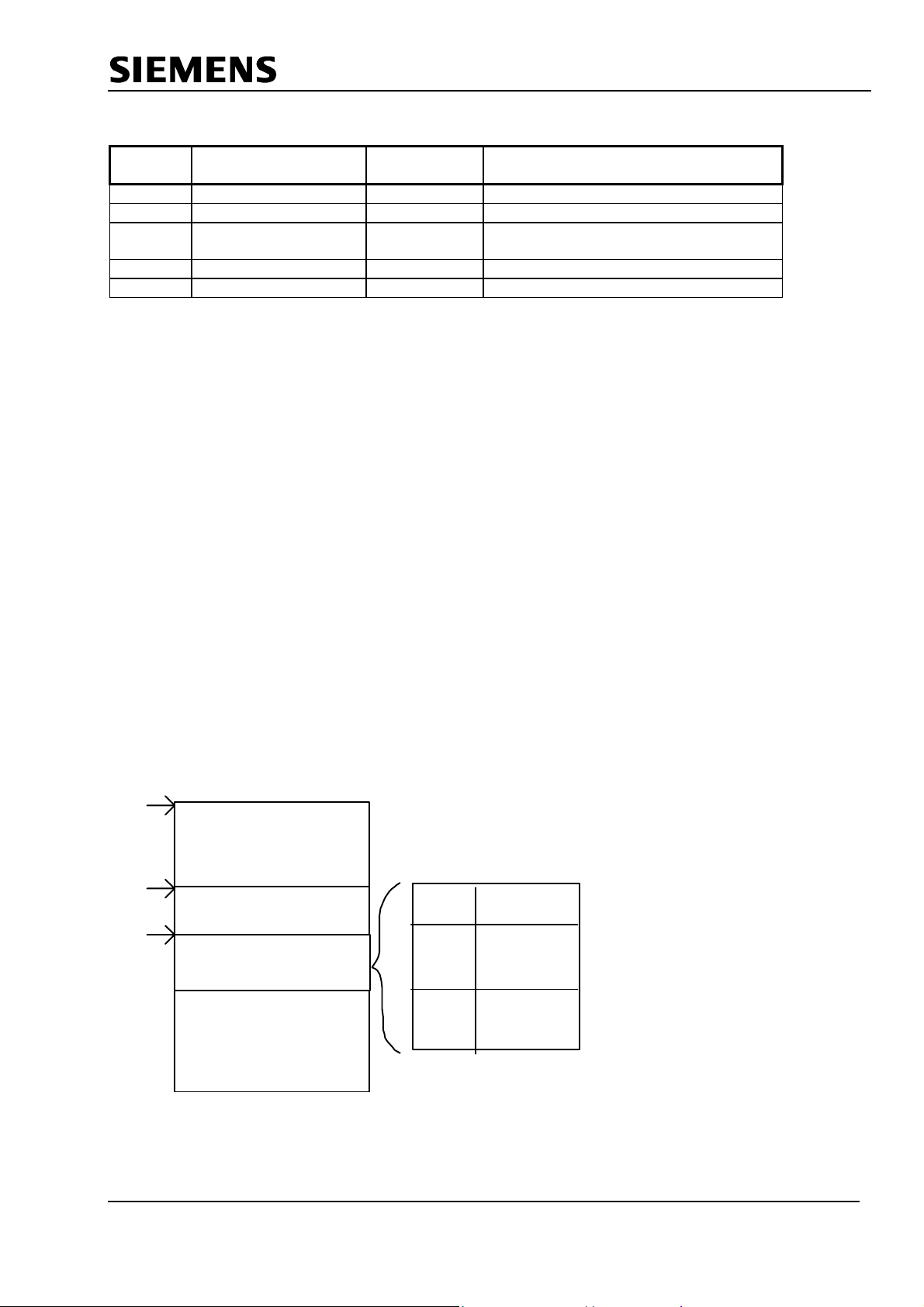
4 Memory Assignment
4.1 Addressing of the SPC4
From the view of the user, the 1.5 kByte internal Dual Port RAM and the internal latches use a 1kByte
address space. Parts of the internal RAM are directly imaged into the address area of the microprocessor;
the other parts can be addressed via a window mechanism.
0H
1FFH
200H
MicroProcessor
512 Byte
General
Parameter
SAP-List
SPC4
0H
1.5 kB RAM
256 Byte
Memory Window
Base Pointer
2FFH
300H
256 Byte
Control Unit
Parameter
3FFH
Figure 4.1 Addressing the Internal 1.5k RAM
The 1k byte address range is divided into four 256 byte blocks with different functions.
Via the lower address window, the FLC can directly access the first 512 (2x256) bytes of the RAM physically
(without having to load the base pointer). This has the advantage that the FLC can access the general
parameters and the SAP list directly, without having to load the base pointer first.
Page 10 Release V1.2 SPC4 User Description
Order Nr. 6GK1 971-5XA00-0BA0 Copyright (C) Siemens AG 1997. All rights reserved.
5FFH
Latches

SPC4 WKF B1 T2
Via the second 256 kByte address window (200h to 2FFh), the entire internal memory can be addressed
with an 8 bit base pointer. The FLC has to load this pointer; it always addresses the beginning of an 8 byte
segment. Thus, the FLC can address up to 256 bytes via the offset address applied to the address pins of
the SPC4.
The third segment which also consists of 256 bytes (300h to 3FFh), addresses the internal latches which are
stored for directly controlling the hardware. These latches are not integrated in the internal RAM area!
Address BitA9Address BitA8Window Select
0 0 Parameter Area (physically 00h-FFh)
0 1 Parameter Area (physically 100h-1FFh)
1 0 entire RAM via Base Pointer
1 1 Parameter Latches
Table 4.1 Window Select
Attention: The hardware won’t prevent overwriting the address area; that is, if the user writes beyond the
station table, the parameters in the lower memory area are overwritten through the wrap-around. In this
case, the SPC4 generates the Mem-Overflow interrupt. If the user writes on write-protected parameters, an
access violation interrupt will be generated.
4.2 Memory Area Distribution of the Internal RAM
4.2.1 Overview
The figure shows the distribution of the internal 1.5k RAM of the SPC4. The entire memory, divided into
segments of 8 bytes each, is broken down into different areas.
Segment 0
BEGIN-PTR
UMBR_PTR
RAM Parameter
SAP-List
SM-SAPs (5x5 byte)
Default-SAP (16 byte)
SAP-0..SAP-63
(64 x 5 byte)
Indication Queue
Reply on IndicationBlocks
Exchange Buffer
Byte 0
Segment 0
Byte 7
Segment 1
Segment 2
Segment 3
Segment 4
Station Table
Ident Buffer
Segment 191
Figure 4.2 Memory Area Distribution
SPC4 User Description Release V1.2 Page 11
Copyright (C) Siemens AG 1997. All rights reserved. Order Nr. 6GK1 971-5XA00-0BA0
WKF B1 T2 SPC4
4.2.2 RAM Parameter Block
In the first 6 bytes of the integrated RAM, the general parameters, such as the read- and write pointers of
the indication queue, are filled which don’t directly engage the control. The FLC is only to write parameters
with the addresses 00H to 5H. The internal user cells are not allowed to be overwritten (the hardware will
generate a write violation interrupt and enter Offline).
Address Name Access Meaning
00H IND-WP-PRE RD/WR The write pointer for early indication processing points to the
next free segment which follows the request message received
last, even if no indication “IND” has been made. The pointer
IND-WP-PRE makes fast slave reaction possible (for example,
for PROFIBUS DP). Immediately after the correct receipt of a
request message (and before a response message is sent), the
pointer IND-WP-PRE is set to the next free segment boundery.
At the same time, the interrupt “IND-PRE” is generated.
01H IND-WP RD/WR The write pointer of the indication queue points to the next free
segment which follows the request message indicated last.
With each indication interrupt “IND”, the SPC4 will set IND-WP
to a new segment boundary.
02H IND-RD RD/WR The read pointer of the indication queue is also a segment
address and is managed by the FLC.
03H FDL-Ident-Ptr RD/WR Pointer to ident-buffer
04H TS-ADR-REG RD/WR Contains station address
05H SAP-MAX RD/WR The highest SAP list number is parameterized
06H..17H internal
working cells
The following cells must not be overwritten (write violation
interrupt)
Table 4.2 Assignment of the RAM Parameter Block
In addition to correctly setting up the corresponding address bits, access to the parmeter latches or the
internal RAM also requires applying an XCS signal to the SPC4. Moreover, the XREADY signal of the
SPC4 has to be noted, or corresponding wait states have to be inserted.
When writing the RAM parameters, the upper, unutilized bits have to be set to ‘0’, while for the
parameter latches, the unassigned bit positions are ‘don’t care’.
4.2.3 SAP List
The SAP list can be addressed directly; segmentation and using the base pointer are not required, but
addressing via the base pointer is also possible. To address the data to which an SAP points, the base
pointer must be used.
The area of the SAPs uses 361 bytes; that is, 46 segments (segment 5...50; of the last segment, only 1
byte is assigned). The SAP list consists of the following:
- 5 SM SAPs (System Management Service Access Point) of 5 bytes each
- DEFAULT SAP with 16 bytes
- 64 SAPs of 5 bytes each
The function of the individual registers and bits is explained in the following chapters.
Page 12 Release V1.2 SPC4 User Description
Order Nr. 6GK1 971-5XA00-0BA0 Copyright (C) Siemens AG 1997. All rights reserved.
SPC4 WKF B1 T2
Address Name Register Meaning
18H SM1 Control Byte Bit Information
19H Request-SA Request-Source Address
1AH reserved
1BH reserved
1CH Reply-Update-Ptr/
SDN-DDB/-Tln-Tab-Ptr
1DH - 21H SM2 see above SM1 see above SM1
22H - 26H SM3 see above SM1 see above SM1
27H - 2BH SM4 see above SM1 see above SM1
2CH - 30H SM5 see above SM1 see above SM1
31H DEFAULT
SAP
32H Request SA Request-Source Address
33H Request SSAP Request-SourceServiceAccessPoint
34H Access Byte Access Protection
35H Reply-Update-Ptr/
36H Reply-Update-Ptr D
37H Reply-Update-Ptr N
38H Reply-Update-Ptr U
39H Response-Buffer-Length
3AH Response Status
3BH Indication-Buffer-Ptr D
3CH Indication-Buffer-Ptr N
3DH Indication-Buffer-Ptr U
3EH Indication-Buffer-Length
3FH Active-Group-Ident
40H Control Command
41H SAP[0] Control-Byte Bit Information
42H Request-SA Request-SourceAddress
43H Request SSAP
44H Access-Byte
45H Reply-Update-Ptr/SDN-DDB/-Tln-
46H - 4AH SAP[1] see above SAP (0) see above SAP(0)
4BH -
17BH
17CH SAP[63] Control-Byte Bit Information
17DH Request-SA Request-SourceAddress
17EH Request SSAP
17FH Access-Byte
180H Reply-Update-Ptr/SDN-DDB/-Tln-
181-187H not used The indication queue has to start at
188H IndicationQueue Start of Indication Queue
SAP[2]-
SAP[62]-
Control Byte Bit Information
SDN-DDB/-Tln-Tab-Ptr
Tab-Ptr
see above SAP (0) see above SAP(0)
Tab-Ptr
Pointer to Response Buffer
Pointer to Response Buffer
Pointer to response buffer
Pointer to Response buffer
the beginning of an 8 Byte segment
Table 4.3: SAP List
SPC4 User Description Release V1.2 Page 13
Copyright (C) Siemens AG 1997. All rights reserved. Order Nr. 6GK1 971-5XA00-0BA0

WKF B1 T2 SPC4
4.2.4 Data Areas in the Internal RAM
4.2.4.1 Indication Queue
The FLC can set the memory area of the indication queue at the segment boundaries.
The BEGIN-PTR is the address of the 1st segment of the indication queue. The end of the queue is marked
by the UMBR_PTR. The UMBR_PTR points to the address of the 1st segment which is not part of the
indication queue.
After initialization, both pointers have to be set to the desired area start in the offline state. THEY
CAN’T BE CHANGED DYNAMICALLY; that is, to modify memory distribution, the SPC4 has to be set
to the offline state. Exchanging the pointer sequence leads to faulty behavior of the SPC4 relative
to the individual memory areas.
If the SPC4 receives request messages, it will enter them in the indication queue. The indication queue is
organized as cyclic buffer (queue); that is, data to be processed is successively entered in the queue as
long as there is enough memory space, while blocks which have been processed are removed. The
indication queues are organized with write- and read pointers. The FLC has to set the indication read
pointer (IND-RP), while the hardware of the SPC4 is responsible for updating the indication write pointer
(IND-WP).
Since it is a cyclic buffer, the end of the queue is to be monitored when data is entered. If the end of the
queue is exceeded, the address has to be wrapped around. For this, the SPC4 offers hardware support
which does the wrap-around automatically.
4.2.4.2 Reply on Indication Blocks
In these buffers, the FLC has to make reply data available. The reply data is assigned to the calls via
pointers in the SAP lists.
4.2.4.3 Exchange Buffers
If PROFIBUS DP services are to be supported (DP mode = 1 in Mode Register 0), six exchange buffers
have to be made available.
4.2.4.4 Ident Buffer
The ident buffer contains the reply data for ident messages.
4.2.4.5 Station Table
The station table is needed for filtering SDN and DDB response messages.
4.2.5 Addressing via the Memory Window
The physical address of the integrated RAM is generated (when addressing the SPC4 via the address
window (200h to 2FFh)) from the base pointer, the segment address for the indication queue and the lower 8
bits of the address bus. For this, the address bus adds the base pointer to the address shifted by 3 bit
positions.
The address is calculated in an ALU which also automatically calculates the address wrap- around when the
queue boundary is exceeded. If the queue boundary is exceeded, the central processor calculates the wrap
around address according to the following pattern:
New segment address = base pointer + AB7..3 - end pointer + start pointer
Together with the 3 least significant address bits, the result is the physical 11bit RAM address for the
memory. After the FLC has loaded the base pointer, it can read up to 256 data bytes through the central
processor, without having to reload the base pointer, and without having to concern itself with the wrap
around at the queue boundary.
Page 14 Release V1.2 SPC4 User Description
Order Nr. 6GK1 971-5XA00-0BA0 Copyright (C) Siemens AG 1997. All rights reserved.

Base Pointer Register
SPC4 WKF B1 T2
+
A10
11 Bit-RAM Address
Address Bus Bit 7..0
A3
Byte Address
within a Segment
Figure 4.3 Calculating the Physical RAM Address
4.3 Assignment of the Parameter Latches
Access to the internal parameter latches -that is, those memory cells which directly intervene in the controlis only possible at the SPC4 via the address window 300H to 3FFH.
These cells can either only be read or written, and in that case, have a different function. In the Motorola
mode, the SPC4 swaps addresses when accessing the address area of 300H (word register); that is, it
exchanges the address bit 0 (it generates from an even address an odd one, and vice versa).
The SPC4 has an 8 bit data interface. When accessing the byte register via this interface, it makes no
difference whether the SPC4 is operated in the Intel- or in the Motorola mode.
When a word register ( two byte register) is accessed, the SPC4 has to decide between Intel and Motorola:
Example: INT-MASK-REG
Intel Mode: write access with address 300
ð INT-MASK-REG (7..0) is written (little endian)
Motorola Mode: write access with address 300
ð INT-MASK-REG (15..8) is written (big endian)
The meaning of the individual bits in the registers is described in more detail in the following chapters.
Since the addresses of the parameters latches are not completely decoded, these registers will reappear at
every 32 bytes. This facilitates implementation since different addresses (names) can be assigned for the
read- and write accesses.
SPC4 User Description Release V1.2 Page 15
Copyright (C) Siemens AG 1997. All rights reserved. Order Nr. 6GK1 971-5XA00-0BA0
WKF B1 T2 SPC4
Addresse
Intel /Motorola
300H 301H Int--Req-Reg 7..0 Interrupt Controller Register
301H 300H Int--Req-Reg 15..8
302H 303H Int-Reg 7..0
303H 302H Int-Reg 15..8
304H 305H Status-Reg 7..0 Status Register
305H 304H Status-Reg 15..8
306H 307H Delay 7..0 Delay Timer Register (actual counter value)
307H 306H Delay 15..8
308H 309H reserved
309H 308H reserved
30AH 30BH reserved
30BH 30AH reserved
30CH- 30FH reserved
310H reserved
311H reserved
312H reserved
313H reserved
314H reserved
315H reserved
316H reserved
317H reserved
318H Mem-Lock 0 Memory Lock Cell
319H reserved
31AH reserved
Name
Meaning (READ Access !)
Figure 4.4 Assignment of the Internal Parameter Latches for READ
Page 16 Release V1.2 SPC4 User Description
Order Nr. 6GK1 971-5XA00-0BA0 Copyright (C) Siemens AG 1997. All rights reserved.

SPC4 WKF B1 T2
Address
Intel /Motorola
300H 301H Int--Mask-Reg 7..0 Interrupt Controller Register
301H 300H Int--Mask-Reg 15..8
302H 303H Int-Ack-Reg 7..0
303H 302H Int-Ack-Reg 15..8
304H 305H TSLOT 7..0 Parameter assignment of Wait-to-Receive time
305H 304H TSLOT 13..8
306H 307H BR-REG 7..0 Parameter assignment of the division factor
307H 306H BR-REG 10..8 for generating the baudrate
308H 309H TID1 7..0
309H 308H TID1 10..8
30AH 30BH FACT-DEL-CLK 7..0 DelayTimer for SM time service
30BH 30AH FACT-DEL-CLK 10..8
30CH- 30F reserved
310H UMBR_PTR S 7..0 UMBR_PTR points to the address of the first
311H Mode-Reg 7..0 Parameter assignment of single bits
312H Mode-Reg1-Res 5..0
313H Mode-Reg1-Set 5..0
314H Base-PTR 7..0 Base address for accesses to the internal RAM
315H TRDY 7..0 Parameter assignment for TRDY (ready time valid
316H PREAMBLE Parameter assignment of number of bits
317H TSYN The following time is parameterized:
318H Mem-Lock 0 Memory Lock Cell
319H BEGIN-PTR 7..0 BEGIN-PTR points to the smallest segment
31AH Mode-Reg2 2..0 Parameter assignment of single bits
Name
Meaning (Write Access !)
segment which is no longer part of the indication
queue
before sending a response message)
(preamble) in the synchron-mode
TSYN (33Bit asynchronous mode)
TIFG (Interframe GAP-Time; synchronous mode)
address of the indication queue. The BEGIN-PTR
have to point at the beginning of an 8 byte
segment.
Figure 4.5: Assignment of the Internal Parameter Latches for WRITE
SPC4 User Description Release V1.2 Page 17
Copyright (C) Siemens AG 1997. All rights reserved. Order Nr. 6GK1 971-5XA00-0BA0

WKF B1 T2 SPC4
5 FLC Interface
5.1 SAP List
5.1.1 Structure of the SAP List
In the FLC, a data transmission service is processed via a Service Access Point (SAP). For each station,
up to 64 SAPs, that is SAP [0..63], are possible at the same time, and the default SAP.
Communication from DEFAULT SAP to a SAP and vice versa is possible. The SPC4 checks the Request
SSAP.
Each SAP (including the DEFAULT SAP) has special entries in the SAP list; via this SAP list, the FLC
makes receive resources available. If the SPC4 receives a message to a SAP which is not available, it will
respond with No Service Activated (SD1 response).
In the SAP list already described, individual registers are assigned to each SAP.
5.1.2 Control Byte
Bit Position Designation
7 6 5 4 3 2 1 0
SAPLocked
SDN/
DDBFilter
RS/RA
or UE
RR IN USE Buffer available Control Byte
Page 18 Release V1.2 SPC4 User Description
Order Nr. 6GK1 971-5XA00-0BA0 Copyright (C) Siemens AG 1997. All rights reserved.
Bit 0-2 Buffer available
The three bits are counters for the resources made available externally. The FLC
increments the 3 bits, as soon as it loads a resource. The SPC4 decrements the 3 bits,
if a received block was indicated. At receipt, after it has received the entire message,
the SPC4 reads the 3 bits. If the status = zero, it will cancel the receipt, set the event
flag ‘No Ressource’ (RR, see below) and respond with No Ressource (SD1-Response)
Exception:
If DP Mode = 1 is set, the SPC4 will not change Buffer Available in the DEFAULT
SAP. Buffer Available has to be parameterized larger than zero, however; otherwise,
the response will be No Resource.
Bit 3 IN USE
The SPC4 will set this bit as soon as it has entered the complete message of a request
message in the indication buffer. It will only reset it if an indication was executed (valid
or invalid). If the FLC wants to assign a new reply block, it has to wait until the bit is
reset. Only then (under Mem-Lock) can it reload the Reply Update Pointer. This
prevents that the FLC can reload data for the SPC4 during transmission operation.
Exception:
If DP Mode = 1 is set, the SPC4 will not set the In Use Bit in the DEFAULT SAP. A
correctly received request message to the DEFAULT SAP will not be entered in the
Indication Queue and not be indicated.
Bit 4
RS/RA or UE
No Service Activated/ Service Access Point Blocked or User-Error: the SPC4 will
set this flag if the plausibilization of Request-SA was negative (Request SA differs from
the SA received ; that is, the call is from an unauthorized station). The SPC4 responds
with Service Access Point Blocked [RA] in the PA-Mode or No Service Activated
[RS] in the Profibus-Mode (SD1-Response). This flag will also be set if Request-SA =
7FH, that is, if the SAP is inactive. The SPC4 responds with No Service Activated
[RS] (SD1-Response). This bit is set as User Error [UE] if the SAP was locked. The
SPC4 responds with User Error [UE] (SD1-Response).
SPC4 WKF B1 T2
Bit 5
Bit 6
Bit 7
Figure 5.1: Control Byte
RR = No Resource
The SPC4 will set this bit if, after receipt of the message header, the content of the
Buffer Available bit = zero; that is, the FLC has made no resources available or the
queue is full. In both cases, the SPC4 will respond with No-Ressource[RR] (SD1-
Response).
SDN-/DDB-Filter
This bit makes it possible to activate the SDN-/DDB filter
0 = The “Reply-Update-Ptr/SDN-/DDB-Tln-Tab-Ptr“ pointer points to the Reply-
1 = The “Reply-Update-Ptr/SDN-/DDB-Tln-Tab-Ptr pointer points to the station
SAP locked
For the moment, the SAP is not accepting data. If the SPC4 receives data for this SAP,
it will set the event flag User Error (UE) and respond with User Error (SD1-Response).
on-Indication block and with that, to the response to be transmitted. If the
pointer = 00H, no response buffer is available, and the SPC4 responds to an
SRD request with a short acknowledgement (SC).
table, and the SPC4 is a “subscriber” for this SAP. The SDN-/DDB-Tln list
will be evaluated at the access “Subscriber for DDB-Response“ and SDNRequest.
SPC4 User Description Release V1.2 Page 19
Copyright (C) Siemens AG 1997. All rights reserved. Order Nr. 6GK1 971-5XA00-0BA0
WKF B1 T2 SPC4
5.1.3 Request SA
The SA received is compared with this entry. If it differs, the SPC4 will set the event flag No Service
Activated (RS) and respond with Service Access Point Blocked [RA] in the PA mode, and with No Service
Activated [RS] in the Profibus mode (SD1 Response). In the case of the default-SAP, the addresses 00H 7EH are possible; in the case of all other SAPs, 80H - FEH (expansion bit set); 7FH leads to “No Service
Activated” since 7FH is locking the SAP. If this entry = FFH (=all), the call won’t be checked. If an SRD is
received with DDB, the bit “SDN-/DDB Filter” will be tested in addition, and if needed, compared further in
the DDB-TIn list, before there is a response or the event flag is set.
5.1.4 Request SSAP
The SSAP received is compared with this entry. If it differs, the SPC4 will set the event flag No Service
Activated (RS) in the PA mode, and Service Access Point Blocked (RA) in the Profibus mode, and respond
with No Service Activated (SD1 Response). If Request SA is 00H-7EH, Request-SSAP = FFh will select
the DEFAULT SAP. If the expansion bit is set in Request SA, and the Request SSAP = FFH, SSAP will not
be checked.
5.1.5 Access Byte
The access byte controls access protection to the matching SAP at receipt. The entry 0H means “no access
protection”. If the SPC4 receives a message that doesn’t match the access byte, it will respond with “NO
SERVICE ACTIVATED”. The event bit RS will be set.
All access violations are filtered to the FLC, the response [RS] (No Service Activated) is transmitted to the
requester. The DDB response (subscriber) is an exception; it is not acknowledged negative.
Bit Position Designation
7 6 5 4 3 2 1 0
IND-N RUP-N Access Value Access Byte
Page 20 Release V1.2 SPC4 User Description
Order Nr. 6GK1 971-5XA00-0BA0 Copyright (C) Siemens AG 1997. All rights reserved.
SPC4 WKF B1 T2
Bit 0-3
Bit 4
Bit 5
Access Value
Access Protection
0H = All
1H = SDN-Low
2H = SDN-High
3H = SDN-Low/High
4H = 5H = SDA-Low
6H = SDA-High
7H = SDA-Low/High
8H = SRD-Low/High DDBREQ DDB-RES-Low/High
9H = SRD Low
AH = SRD-High
BH = SRD-Low/High
CH = DDB-REQ
DH = DDB-RES-low
EH = DDB-RES-high
FH = DDB RES low/high
RUP-N-Valid (Only for DEFAULT SAP)
This bit is set by the application, if in the DP-Mode, valid input data is entered in the
Reply-Update-Buffer N. The SPC4 will reset the RUP-N-Valid, after it has
exchanged the Reply Update Buffers D and N
IND-N-Valid (Only for DEFAULT SAP)
This bit will be set by the SPC4 if in the DP mode, valid output data is entered in
Indication Buffer N . The FLC will reset IND-N-Valid after the FLC has exchanged
the Indication Buffers N and U.
Figure 5.2 Access Byte
5.1.6 Reply Update Ptr/ SDN-DDB-TIn-Tab-Ptr
The Reply Update Ptr/ SDN-DDB-TIn-Tab-Ptr pointer points to the Indication Reply Buffer, or to the SDN/DDB-TIn list (see also SDN-/DDB filter). The data buffers have to be above the UMBR_ PTR in the SPC4.
The SDN-/DDB-TIn list has the following structure:
SDN-/DDB-Tln List (optional)
tab-data-length 8 Bit indicates the length of the SDN-/DDB-Tln list
don’t care 8 Bit
Request-SA 1 8 Bit 1st entry in the DDB-Tln list Meaning like Request-SA
Request-SSAP 1 8 Bit 1st entry in the DDB-Tln list Meaning like Request-SSAP.
........
Request-SA n 8 Bit n entry in the DDB-Tln list Meaning like Request-SA
Request-SSAP n 8 Bit n entry in the DDB-Tln list Meaning like Request-SSAP.
Figure 5.3: SDN-/DDB List
All SDN messages (except SM TIME; it is always indicated and DDB response messages can be filtered by
the SPC4 via the station table. In this station table, the “Request SA” and the “Request SSAP” are defined
per entry. Only if the received SDN-/DDB message with one of the entries is plausible, there will be an
indication.
The SDN-/DDB filter is active if the bit “SDN/DDB filter” is set in the receive-SAP. The station table is
addressed by the pointer “SDN-/DDB-TIn-Tab-Ptr”. If “tab-data-length” = 0, the SDN-/DDB-TIn list is not
plausibilized.
SPC4 User Description Release V1.2 Page 21
Copyright (C) Siemens AG 1997. All rights reserved. Order Nr. 6GK1 971-5XA00-0BA0

WKF B1 T2 SPC4
In order to make it possible for the sender to process via the DEFAULT-SAP, “req-ssap=0FFh” and the
expansion bit “req-sa” = 0 has to be entered in the station table on the receiver side. In all other cases, the
expansion bit “req-sa” = 1 is set.
5.1.7 Special Features for the DEFAULT SAP
When using the DP mode, the following entries are also to be processed in the SAP list.
• • Reply Update Ptr D,N,U:
These 8 bit pointers point to the 1st segment respectively of the Reply Update Buffers D, N and U. In
the Reply Update Buffer U, the FLC compiles the input data, and then exchanges the U-Buffer with the
Reply Update Buffer N. The SPC4 responds to a request message with the input data from the Reply
Update Buffer D. The SPC4 receives new input data by exchanging the D and N buffer. The Reply
Update Buffers D, N and U only contain net data.
• • Response Buffer Length:
This value specifies the length of the Reply Update Buffers D, N and U (0 to 246 bytes).
• • Response Status:
specifies the priority of the response messages to the DP master. 2 values are permitted:
- 08H: response low priority
- 0AH: response high priority
• • Indication Buffer Ptr D, N and U:
These 8 bit pointers point respectively to the 1st segment of the Indication Buffers D, N and U. In the
Indication Buffer D, the SPC4 enters output data received faultlessly from the master, and then
exchanges (possibly not until Sync, see Chapter 2.7) the D-Buffer with the Indication Buffer N. The
output data of the FLC is in the Indication Buffer U.The FLC receives new output data by exchanging
Indication Buffer U and N. The Indication Buffers D, N and U only contain net data.
• • Indication Buffer Length:
This value specifies the length of the Indication Buffers D, N and U (0 to 246 bytes).
• • Active Group Ident:
This byte encodes the association of the DP slave with 8 groups maximum. Active group ident is ANDoperated bit by bit with the group select byte of a received Global Control Message (GCM). The DP
slave is addressed if the bit by bit AND operation supplies a value unequal to zero at at least one
position. If the group select byte of the GCM = zero, all DP slaves are addressed.
• • Control Command of a Global Command Message
Here, the SPC4 enters the last received control command of a global control message.
5.2 SM-SAP List
The structure of the SM-SAP entries is analog to the normal SAPs.
Register Meaning
Control Byte Bit Information
Request SA Request SourceAddress
reserved
reserved
Reply-Update-Ptr/SDN-DDB/-Tln-
Tab-Ptr
Pointer to Reply Buffer
SAPs which are not needed are to be deactivated; for example, with Request SA=7FH.
Page 22 Release V1.2 SPC4 User Description
Order Nr. 6GK1 971-5XA00-0BA0 Copyright (C) Siemens AG 1997. All rights reserved.
SPC4 WKF B1 T2
SAP Service Transmission
Description
Function Code
SM1 SM_SDN 2 SM-SDN messages
SM2 SM_SRD_SLOT_DEL 10 SM-SRD-Slot-Del messages
SM3 SM_SRD_SLOT_KEEP11 SM-SRD-Slot-Keep messages
SM4 SM_SRD 1 SM-SRD messages
SM5 SM_Time 0 SM-Time messages
Figure 5.4 SM SAP list
The use of the SM-SAPs depends on the control octet. No SAP expansions are used, analog to the use of
the DEFAULT-SAP.
The SPC4 recognizes from the message received (CO field) which SM service is to be executed, and
assigns it autonomously to the matching SAP (see table).
Like all other messages, the services SM_TIME and SM_SDN are transferred to the Indication Queue; no
resources are needed for transmission (slave).
5.3 Indication Queue
5.3.1 Description
If the SPC4 receives a message, it will enter the message header in the indication queue, and then check
the free length in the queue (this is possible, because one segment always has to remain free). If at least
one segment (8 bytes) is free (in addition to the spec. free segment), it will continue receiving and enter the
data in the queue as long as free memory is available. When receiving a request message (call), the SPC4
plausibilizes the corresponding message headers with the values specified for it from the SAP list.
The Indication Queue is managed as circular buffer with read- (IND-RD) and write pointers (IND-WR). The
SPC4 is responsible for the write pointer, and the FLC for the read pointer.
The pointer IND-WR-PRE makes fast slave reaction possible (for DP, for example). An indication interrupt
will be generated (if corresponding parameter was assigned) after the correct receipt of the request
message, and not at the end of the next message to another station.
BEGIN-PTR
IND-RD
IND-WR
Indication Queue
Indication Block n-1
Indication Block n
Indication-Block
Response
Header
(2 Byte)
Request
Header
(6 Byte)
Request
Buffer
(max. 246
Byte)
resp-buf-ptr (8 Bit)
indic-status
(00 valid, CFH invalid)
req-data-length
rem-adr
loc-adr
co-code
rem-sap
loc-sap
Figure 5.5: Structure of the Indication Queue
If a message is received without SAP expansion (rem SAP, loc SAP), the SPC4 will enter 0FFh in the
corresponding cell.
SPC4 User Description Release V1.2 Page 23
Copyright (C) Siemens AG 1997. All rights reserved. Order Nr. 6GK1 971-5XA00-0BA0

WKF B1 T2 SPC4
Page 24 Release V1.2 SPC4 User Description
Order Nr. 6GK1 971-5XA00-0BA0 Copyright (C) Siemens AG 1997. All rights reserved.

5.3.2 Structure of the Indication Block
SPC4 WKF B1 T2
SPC4 User Description Release V1.2 Page 25
Copyright (C) Siemens AG 1997. All rights reserved. Order Nr. 6GK1 971-5XA00-0BA0

WKF B1 T2 SPC4
Response Header
Byte 0 resp-buf-ptr This pointer points to the relocated response buffer (in the area Reply-On-
Indication blocks, see Memory Area Distribution). It is recopied by the SPC4
from the SAP list
Byte 1 indic-status Here, the SPC4 enters the status 00 for a ‘valid indication’.
Request-Header (Message Header of the Requester)
Byte 2 req-data-
length
Byte 3 rem-adr Here, the SPC4 enters the SA received. The remote station, which is to
Byte 4 loc-adr Here, the SPC4 enters DA received.
Byte 5 co-code This value specifies the function code of the request message. Here, the
This value specifies the length of the entered net data in the request buffer (0
to 244 Bytes with SAP expansion, 0 to 246 bytes without SAP expansion).
maintain data traffic with the respective SAP of the local station {sentence
not quite clear in original}. It can be entered in the SAP lists under req-sa as
filter.
complete control octet, as received from the bus, is entered.
Function Code
Request FDL-Status with Reply x9H
Send Data with no Acknowledge low x4H
Send Data with no Acknowledge high x6H
Send Data with Acknowledge low x3H
Send Data with Acknowledge high x5H
Send and Request Data low xCH
Send and Request Data high xDH
SM_Time x0H
SM_SRD x1H
SM_SDN x2H
SM_SRD_SLOT_DEL xAH
SM_SRD_SLOT_KEEP xBH
Send and Request Data with DDB x7H
DDB-Response low y8H
DDB-Response high yAH
x:
Frame Type 1; that is, Bit 6=1 and FCB/FCV according to message entry
y:
Frame Type 0; that is, Bit 6=0 and station type1 according to message entry
Bit 7 (b8) of the control octet received is only evaluated for SM time
messages; for all other request messages, bit 7 (b8) of the control octet is
don´t care
Byte 6 rem-sap Here, the SPC4 enters the service access point (SSAP) of the remote
station. This field is only valid if the expansion bit in rem-adr is set (the two
upper bits of rem-sap have to be ‘0’ ). If a message is received without SAP
expansion (rem-SAP, loc-SAP), the SPC4 will enter 0FFh .
Byte 7 loc-sap Here, the SPC4 enters the service access point (DSAP) of the local station.
This field is only valid if the expansion bit in rem-adr is). If a message is
received without SAP expansion (rem-SAP, loc-SAP), the SPC4 will enter
0FFH .
Request Buffer contains the received message
Byte 8 data 0 Byte 0 of the net data
Byte
data 0+x Byte x of the net data
8+x
Figure 5.6: Indication Block
1
Note: For PROFIBUS, the station-type is bit 5 (b6) und bit 4 (b5), for PA bit 7 (b8) is relevant in addition.
Page 26 Release V1.2 SPC4 User Description
Order Nr. 6GK1 971-5XA00-0BA0 Copyright (C) Siemens AG 1997. All rights reserved.
SPC4 WKF B1 T2
5.4 Reply on Indication Blocks
5.4.1 Function
The FLC has to load response data in the buffers of the Reply-on-Indication blocks.
If response data is requested, the SPC4 will fetch the reply update pointer from the corresponding SAP lists,
and transmit the loaded data from the reply buffer. If the request is processed, the SPC4 will indicate {index}
the request by entering the status (valid indication) in the response buffer, setting the write pointer to the
next free segment and generate the interrupt IND.
A request is processed and will be indicated if:
• an SM message, an SDN- or a DDB response message was received faultlessly.
• an SDA- or SRD message was received faultlessly, the response has been transmitted and the next
request message to another station or (with toggeled FCB/FCV bits) to its own station address was
received correctly.
If the SPC4 receives an SRD- or a DDB request message with net data length = 0, and if the response data
length also = 0, the SPC4 will not enter this message in the indication queue(empty polling).
With a bit in the responder status (byte 2), the FLC can control how often the loaded data is transmitted
from the indication reply buffer. If Bit (4):single update reply is set in “resp-status” of the indication reply
buffer, a loaded response in the indication reply buffer is transmitted only once. If this bit = log. “0”, the
SPC4 will again transmit the buffer to this SAP with each call message (multiple update reply).
The less significant nibble (lower 4 bits) indicates whether the request is transmitted high priority or low
priority.
5.4.2 Structure of the Reply-on-Indication Blocks
Area of Reply-on-Indication Blocks
WRAP AROUND
-PTR1
Indication Reply Buffer
Indication Block
Byte 1
Byte 2
Net Data
Buffer of Responder
resp-buf-ptr
Reply-Update-PTR
(SAP List)
resp-buf/data-length
resp-status
(08h,18h: low priority
0Ah,1Ah high priority)
Figure 5.7: Structure of Reply-on-Indication Block
The response buffer is attached to the area ‘Reply on Indication Blocks’ and contains the response buffer
length, the response status and the pure net data of the response message.
SPC4 User Description Release V1.2 Page 27
Copyright (C) Siemens AG 1997. All rights reserved. Order Nr. 6GK1 971-5XA00-0BA0

WKF B1 T2 SPC4
Reply Header
Byte 0 resp-data-
length
Byte 1 resp-status In this field, the responder status is stored. The FLC has to load the
Reply Buffer contains the response data
Byte 3 data 0 Byte 0 of the net data
Byte
8+x
Figure 5.8: Reply-on-Indication Block
data 0+x Byte x of the net data
Here, the FLC enters the length of the response buffer.
status. The following codes are permitted:
Function Code
Response FDL/FMA1/2-data low
(& Send Data OK)
Response FDL/FMA1/2-data high
(& Send Data OK)
Bit (4) = x :Single Update Reply
If this bit is set in addition, a reply loaded in the indication buffer is
transmitted only once. Otherwise, the SPC4 will retransmit this buffer
for each reply message
000x1000b
000x1010b
Page 28 Release V1.2 SPC4 User Description
Order Nr. 6GK1 971-5XA00-0BA0 Copyright (C) Siemens AG 1997. All rights reserved.

SPC4 WKF B1 T2
6 DP Interface
6.1 Description
In the PROFIBUS DP mode (DIN 19245 Part 3), the SPC4 supports the following productive services:
• • Data Exchange
• • Read Input Data
• • Read Output Data
• • Global Control (Sync, Freeze, Clear Data)
Other PROFIBUS DP services (diagnosis, parameterisation and configuration) have to be realized by the
FLC; that is, the software has to operate the corresponding SAPs according to the PROFIBUS DP state
machine.
For the above named services to be supported by the SPC4, DP Mode = 1 is to be set in Mode Register 0.
In the DP mode, data between the DEFAULT SAP of the DP master and the DEFAULT SAP of the DP
slave is exchanged with exchange buffers:
For received data (output data), the Indication Buffers D, N and U are available. For the response data
(input data), the Reply Update Buffers D, N and U are used.
No indication interrupts will be generated. If new output data is made available to the FLC, the interrupt
“Output Data Exchange” will be generated. The interrupt “Watchdog Reset” indicates that valid output data
from the DP master to the DEFAULT SAP was received. The interrupt “Watchdog Reset” causes the FLC
to reset the “Software Watchdog” which monitors the activity of the DP master.
Request messages to an SAP other than the DEFAULT SAP are only accepted if SSAP differs from
DEFAULT SAP. Request SSAP has to be parameterized by the FLC correspondingly. The received data is
entered in the indication queue. The reply is made with the data of the Reply Update Buffer to which the
Reply Update Pointer of the addressed SAP points. If the received request data is entered in the indication
queue, the pointer “IND-WP-PRE” is set to the next free segment, and the interrupt “IND-PRE” is generated.
If the request is processed, the pointer IND-WP is also set to the next free segment and the interrupt “IND”
is generated (indication).
The figure below shows the principle of the exchange buffer:
Exchange Exchange
through FLC
Buffer
U
Buffer
D
through SPC 4
Buffer
N
Figure 6.1: Exchange Buffer Principle
In the Indication Buffer D, the SPC4 enters output data to the local DEFAULT SAP, received faultlessly
from the DEFAULT SAP of the DP master. The SPC4 generates the interrupt “Watchdog Reset”. Then, the
SPC4 exchanges the Indication Buffers D and N either immediately (DIAG.SYNC Mode = 0), or with the
next “Sync” command (DIAG.SYNC Mode = 1). After exchanging the Indication Buffer Pointers D and N,
the SPC4 will set the flag IND-N-Valid = 1 in the DEFAULT SAP, and generate the interrupt “Output Data
Exchange”.
SPC4 User Description Release V1.2 Page 29
Copyright (C) Siemens AG 1997. All rights reserved. Order Nr. 6GK1 971-5XA00-0BA0

WKF B1 T2 SPC4
These indications are carried out under Lock to guarantee data consistency. If the FLC wants to update its
output data in the Indication Buffer U, it has to check first whether IND-N-Valid = 1 (that is, whether valid
output data is entered in the Indication Buffer N). If this is the case, the FLC can update its output data by
exchanging the Indication Buffers N and U. In addition, the FLC has to reset the flag IND-N-Valid = 0 in the
DEFAULT SAP. The FLC has to carry out these actions under Lock.
In the Reply Update Buffer U, the FLC combines the input data, and then exchanges the U buffer with the
Reply Update Buffer N. In addition, the FLC has to set the flag RUP-N-Valid = 1 in the DEFAULT SAP
when the Reply Update Pointers U and N are exchanged. The FLC has to carry out these actions under
Lock. If the DP master requests input data with a request message, the SPC4 will respond
• either with the “old” input data of Reply Update Buffer D (that is, Reply Update Buffer D and N are not
exchanged before the response is transmitted). This is the case if no valid input data is entered in the
Reply Update Buffer N (that is, RUP-N-Valid = 0 in the DEFAULT SAP) or the input data in the Reply
Update Buffer D is frozen (DIAG.FREEZE Mode = 1, see Chapter 2.7.4);
• or with the “new” input data, if before transmitting the response, the Reply Update Buffers D and N are
exchanged. The buffers are exchanged if RUP-N-Valid = 1 and DIAG.FREEZE Mode = 0. Then, the
SPC4 will set the flag RUP-N-Valid = 0 in the DEFAULT SAP. The buffers are exchanged and the flag
RUP-N-Valid is reset under Lock.
6.2 Productive Services
6.2.1 Data Exchange
The control unit for the PROFIBUS DP protocol is to be realized by the FLC. As DP slave, the SPC4 is
permitted to receive request message from the DEFAULT SAP of the DP master to its own DEFAULT SAP
only if the DP control unit is in the mode “data exchange” . Therefore, the FLC has to parameterize
Request SA - Station Address of the DP Master
in the DEFAULT SAP. In all other DP modes (for example Wait-PRM, Wait-Config), the FLC has to
deactivate the DEFAULT SAP with
Request SA = 7FH
A request message by the DP master to the DEFAULT SAP would in this case be rejected with “No Service
Activared” (RS).
In the DEFAULT SAP of the SPC4,
Request SSAP = FFH (for DEFAULT SAP)
Access Value = 08H
is to be parameterized in the DP mode.
Access Value = 08 filters all request messages except
• Send and Request Data low (SRD low)
• Send and Request Data high (SRD high)
• Send and Request Data with DDB (DDB Request)
• DDB Response low
• DDB Response high
The transpparence for DDB response low/high messages makes it possible for the SPC4 to listen in on the
bus as slave also via the DEFAULT SAP, and to evaluate the received data. Since, as a rule, the publisher
is not going to be the DP master, the SDN-/DDB filter is to be activated. If the SDN-/DDB filter bit is set in
the control byte of the DEFAULT-SAP, the source address (SA) and SSAP are plausibilized exclusively in
Page 30 Release V1.2 SPC4 User Description
Order Nr. 6GK1 971-5XA00-0BA0 Copyright (C) Siemens AG 1997. All rights reserved.

SPC4 WKF B1 T2
the SDN-/DDB station list. Received DDB response messages are entered in the indication queue. Then
the pointers “IND-WP-PRE” and “IND-WP” are set to the next free segment, and the interrupts “IND-PRE”
and “IND” are generated.
If an SRD low/high message is received from the DP master, and no input data is available (that is,
response buffer length = 0), the SPC4 will reply
• either with SC, if 08H (that is, low priority) is entered in the response status of the DEFAULT SAP
• or with an SD2 message with the length LE = 4 and FFH as dummy byte (that is, net data length = 1), if
0AH (that is high priority) is entered in the response status of the DEFAULT SAP.
If a DDB request is received from the DP master and no input data is available (that is, response buffer
length = 0), the SPC4 replies with “No Service Activated (RS)” and sets the RS flag in the control byte of the
DEFAULT SAP.
6.2.2 Read Input Data
Read Input Data is an SRD message without request data, by any bus master, with SSAP different from
DEFAULT SAP, to the SAP 56 of the DP slave. As DP slave, the SPC4 is permitted to evaluate this
message only if the DP control unit is in the mode “data exchange”. In all other modes (for example, Wait
PRM, Wait Config), SAP 56 is to be deactivated by the FLC with Request SA = 7FH. A Read Input Data
message would in this case be rejected with “No Service Activated (RS)”.
In the SAP 56 of the SPC4, the following is to be parameterized in the DP mode “Data Exchange”:
Buffer Available > 0
Request-SA = FFH (all)
Request-SSAP = SSAP (different than DEFAULT-SAP)
Access Value = {09H, 0AH, 0BH}
Reply Update Ptr / SDN-/DDB-TIn-Tab-Ptr = don´t care
Read Input Data messages are not indicated by the SPC4 and are not entered in the indication queue. In
the control byte of SAP 56, Buffer Available is not decremented.
If input data is requested with Read Input Data, the SPC4 will respond
• either with the “old” input data of Reply Update Buffer D (that is, Reply Update Buffer D and N are not
exchanged before the response is transmitted). This is the case if no valid input data is entered in the
Reply Update Buffer N (that is, RUP-N-Valid = 0 in the DEFAULT SAP), or the input data in the Reply
Update Buffer D is frozen (DIAG, FREEZE Mode = 1, see Chapter 2.7.4);
• or with the “new” input data, if before transmitting the response, the Reply Update Buffers D and N are
exchanged. The buffers are exchanged if RUP-N-Valid = 1 and DIAG, FREEZE Mode = 0 in the
DEFAULT SAP. Then, the SPC4 will set the flag RUP-N-Valid = 0 in the DEFAULT SAP. The buffers
are exchanged and the flag RUP-N-Valid is reset under Lock.
If the response buffer length = 0 is parameterized in the DEFAULT-SAP, the SPC4 will respond with SC.
An SRD message with request data to the SAP 56 of the DP slave is rejected by the SPC4 with “No
Resource (RR)”.
SPC4 User Description Release V1.2 Page 31
Copyright (C) Siemens AG 1997. All rights reserved. Order Nr. 6GK1 971-5XA00-0BA0

WKF B1 T2 SPC4
6.2.3 Read Output Data
Read Output Data is an SRD message without request data by any bus master, with SSAP different from
DEFAULT SAP, to the SAP 57 of the DP slave. As DP slave, the SPC4 is permitted to evaluate this
message only if the DP control unit is in the mode “data exchange”. In all other modes (for example, Wait
PRM, Wait Config), SAP 57 is to be deactivated by the FLC with Request SA = 7FH. In this case a Read
Output Data message would be rejected with “No Service Activated (RS)”.
In the SAP 57 of the SPC4, the following is to be parameterized in the DP mode “Data Exchange”:
Buffer Available > 0
Request-SA = 0FFH (all)
Request-SSAP = SSAP (different than DEFAULT-SAP)
Access Value = {09H, 0AH, 0BH}
Reply Update Ptr / SDN-/DDB-Tln-Tab-Ptr = don´t care
Read Output Data messages are not indicated by the SPC4 and are not entered in the indication queue. In
the control byte of SAP 57, Buffer Available is not decremented.
Read Output Data causes the SPC4 to respond with the output data of the Indication Buffer U.
If the indication buffer length = 0 is parameterized in the DEFAULT SAP, the SPC4 responds with SC.
An SRD message with request data for the SAP 57 of the DP lave is rejected by the SPC4 with “No
Resource(RR)”.
6.2.4 Global Control (Sync, Freeze, Clear Data)
The global control message is an SDN message with 2 bytes net data from the DP master with SSAP =
DEFAULT SAP, to the SAP 58 of the DP slave. As DP slave, the SPC4 is permitted to evaluate this
message only if the DP control unit is in the mode “data exchange”. In all other modes (for example, Wait
PRM, Wait Config), SAP 58 is to be deactivated by the FLC with Request SA = 7FH. In this case a global
control message would be rejected with “No Service Activated (RS)”.
In the SAP 58 of the SPC4, the following is to be parameterized in the DP mode “Data
Exchange”:
Buffer Available > 0
Request-SA = station address of the DP master
Request-SSAP = SSAP (different than DEFAULT-SAP)
Access Value = {01H, 02H, 03H}
Reply Update Ptr / SDN-/DDB-Tln-Tab-Ptr = don´t care
In the control byte of SAP 58, Buffer Available is not decremented. A global control message with a net
data length unequal to 2 is not evaluated by the SPC4 if “Check GCM-Length-Off = 0” is parameterized in
Mode Register 2.
With Check GCM-Length-Off = 1, monitoring of the net data length of GCMs is switched off.
The function Global Control makes it possible to transmit a special control command to one (single), several
(multi) or all (broadcast) DP slaves. The figure below shows the data format of the 2 user bytes.
Address Bit Position Designation
7 6 5 4 3 2 1 0
Byte 0 Res Res Sync Unsync Freeze Unfreeze Clear_
Data
Byte 1 Select7Select6Select5Select4 Select3 Select2 Select1 Select0 Group Select
Res Control
Command
Page 32 Release V1.2 SPC4 User Description
Order Nr. 6GK1 971-5XA00-0BA0 Copyright (C) Siemens AG 1997. All rights reserved.

SPC4 WKF B1 T2
Byte 0: Control Command
Bit Designation Meaning
0 Reserved The designation “Reserved” indicates that these bits are reserved
for future function expansions, and are to be preassigned with “logic
0”.
If the bit “Check-GCM-Resbits-Off = 0 in Mode Register 2, the
reserved bits will be checked for zero. If at least one of these
reserved bits is “logic 1”, the SPC4 will execute “Leave Master”.
If Check-GCM-Resbits-Off = 1, the reserved bits are don’t care for
the SPC4.
1 Clear_Data Output data in the indication buffer is deleted, and the interrupt
Output_Data_Exchange is generated
2 Unfreeze If Unfreeze is set, the SPC4 deactivates the Freeze Mode
(DIAG.FREEZE Mode = 0) and exchanges the Reply Update
Buffers D and N if the flag RUP-N-Valid = 1 in the DEFAULT SAP.
Then, the SPC4 will set RUP-N-Valid = 0. These actions are carried
out under Lock.
If DIAG.FREEZE Mode = 0, the SPC4 will respond to a request
message which is requesting input data with the “new” input data;
that is, before transmitting the response, the SPC4 exchanges the
Reply Update Buffers D and N if the flag RUP-N-Valid = 1 in the
DEFAULT SAP.
3 Freeze If Freeze is set, the SPC4 will activate the Freeze Mode
(DIAG,FREEZE Mode = 1) and exchange the Reply Update Buffers
D and N if the flag RUP-N-Valid = 1 in the DEFAULT SAP. Then,
the SPC4 will set RUP-N-Valid = 0. The SPC4 executes these
actions under Lock. If, in the Freeze Mode, input data is requested
from the SPC4 with a request message, the SPC4 will respond with
the “old” input data of Reply Update Buffer D; that is, the Reply
Update Buffers D and N will not be exchanged prior to transmitting
the response.
4 Unsync If Unsync is set, the SPC4 deactivates the Sync Mode (DIAG.SYNC
Mode = 0), and exchanges the Indication Buffer D and N if valid
data is {entered} in the D buffer. In addition, it will set the flag INDN-Valid = 1 in the DEFAULT SAP and generate the interrupt
“Output Data Exchange”.
If DIAG.SYNC Mode = 0 when a global control message with
Unsync = 1 is received, Unsync will have no effect.
If DIAG.SYNC Mode = 0, the SPC4 exchanges the Indication
Buffers D and N immediately if it has received new valid output
data.
5 Sync If Sync is set, the SPC4 will activate the Sync Mode (DIAG.SYNC
Mode = 1) without exchanging the Indication Buffers D and N. If
DIAG.SYNC Mode = 1 when a global control message is received
with Sync = 1, the SPC4 exchanges the Indication Buffers D and N
if valid output data is {entered} in the D-buffer. In addition, it will set
the flag IND-N-Valid = 1 in the DEFAULT SAP, and generate the
interrupt “Output Data Exchange”. The SPC4 executes these
actions under Lock.
If DIAG.Sync Mode = 1, the SPC4 enters new output data from the
DP master in the Indication Buffer D and generates the interrupt
“Watchdog Reset”. The SPC4 waits with the exchange of the
Indication Buffers D and N, however, until the next “Sync”
command.
6,7 Reserved
Figure 6.2 Global Control
SPC4 User Description Release V1.2 Page 33
Copyright (C) Siemens AG 1997. All rights reserved. Order Nr. 6GK1 971-5XA00-0BA0

WKF B1 T2 SPC4
Byte 1: Group Select
Group Select specifies which groups are to be addressed by the DP slaves.
The SPC4 AND-operates the Group Select byte of a received global control message bit by bit with the byte
“Active Group Ident” of the DEFAULT SAP. The DP slave is addressed if the bit by bit AND operation
supplies a value unequal to zero on at least one position {location}.
If the Group Select byte = 00H, all DP slaves are addressed.
If the control command of a global control message (GCM) is different than the control command in the
DEFAULT SAP, the SPC4 will enter the GCM in the indication queue and generate the indication interrupt.
In addition, the received control command is stored in the DEFAULT SAP.
6.2.5 Leave Master
In the case of Leave Master, the SPC4 will carry out the following actions:
• output data in the indication buffer is deleted; that is 00H is entered {?}
• then, the Indication Buffers D and N are exchanged (under Lock)
• the interrupt “Output Data Exchange” is not generated
• DEFAULT SAP, SAP 56, SAP 57, SAP 58 are deactivated; that is, under Lock,
Request SA = 7FH is entered in all 4 SAPs
• generate interrupt “leave master”
The SPC4 will execute “Leave Master” if
• the bit Cmd-Leave-Master = 1 is set in Mode Register 1:
at the end of “Leave Master”, the SPC4 will reset Cmd-Leave-Master
to “logic 0” in Mode Register 1
• in the control command of a GCM, at least 1 reserved bit is “logic 1”,
and in Mode Register 2 Check-GCM-Resbits-Off = 0 is parameterized
• the received net data length of a DP data message is less than the
indication buffer length in the DEFAULT SAP:
The SPC4 responds with input data from the Reply Update Buffer D; if
DIAG.FREEZE mode = 0 and RUP-N-Valid = 1, the Reply Update Buffers
D and N will be exchanged first
• the received net data length of a DP data message is larger than the
indication buffer length in the DEFAULT-SAP:
The SPC4 responds with “No Resource (RR)”, and sets the RR flag in the
control byte of the DEFAULT SAP to “logic 1”.
The execution time tLM which the SPC4 needs for “Leave Master”, is dependent on the indication buffer
length n and the baudrate
12 MBaud: (25 + n) bit pulses <= t
To baudrates less than 3 M Baud, the following applies:
(30 + 1.5 n) bit pulses
LM <=
tLM ≈ (20 + n/2) bit pulses
Attention:
In the case of "Leave-Master", the danger exists that request messages to the SPC4, which were received
during the execution time tLM will be lost. Since, during this time t
receive but can’t be flushed, the interrupt "FIFO-Overflow" is possible.
Page 34 Release V1.2 SPC4 User Description
Order Nr. 6GK1 971-5XA00-0BA0 Copyright (C) Siemens AG 1997. All rights reserved.
the receiver of the SPC4 is ready to
LM ,

SPC4 WKF B1 T2
6.2.6 Baudrate Search
If the bit “Baudrate Search” is set in Mode Register 1, the automatic baudrate search is switched on. In this
mode, the SPC4 doesn’t evaluate messages; it only checks whether a message was received faultless
physically. In order to be able to also receive reply messages, the T
regardless of the value which was parameterized in the SYN time register. If the receipt is faulty, the
interrupt “wrong SD” will be generated. If SD4 or a complete SD1/SD2/SD3 message is received faultlessly,
the interrupt “correct SD” is generated. A faultlessly received SC is ignored.
The baudrate which is to be checked respectively has to be parameterized by the FLC.
is reduced to 10 bit pulses,
SYN
SPC4 User Description Release V1.2 Page 35
Copyright (C) Siemens AG 1997. All rights reserved. Order Nr. 6GK1 971-5XA00-0BA0

WKF B1 T2 SPC4
7 ASIC Interface
Below, the registers will be described which specify the hardware function of the ASIC as well as message
processing.
Parameters which intervene directly in the control, or sephamores which are directly set by the control, are
stored in the SPC4 in a parameter latch array. All other parameters are in the lower area of the RAM. In
the parameter cells, the FLC transfers operating data to the FLC. Parameters are assigned only in the
offline state (for example, after switch on). The SPC4 must leave the offline state only after all parameters
have been loaded (START SPC4 = 1, Mode Register 1). Some control bits, however, have to be changed
continuously during operation. These are combined in a special register (Mode Register 1) and can be set
or deleted independent of one another.
7.1 Latch Parameters
7.1.1 Slot Time Register
(writable; can only be changed offline)
Address Bit Position Designation
Control
Register
304H
(Intel)
7 6 5 4 3 2 1 0
TSL7 TSL6 TSL5 TSL4 TSL3 TSL2 TSL1 TSL0 TSLOT
7..0
Address Bit Position Designation
Control
Register
305H
(Intel)
Figure 7.1: Slot Time Register
The Wait-to-Receive time TSL is 14 bits wide maximum, and to be entered in transmission bit steps. It is
needed to calculate timeout.
7.1.2 Baudrate Register
(writable; can only be changed offline)
Address Bit Position Designation
Control
Register
306H
(Intel)
Address Bit Position Designation
Control
Register
307H
(Intel)
15 14 13 12 11 10 7 8
TSL13 TSL 12 TSL 11 TSL 10 TSL 9 TSL8 TSLOT
13..8
7 6 5 4 3 2 1 0
BR7 BR6 BR5 BR4 BR3 BR2 BR1 BR0 BR-Reg
7..0
15 14 13 12 11 10 7 8
BR 10 BR 9 BR8 BR-REG
10..8
Figure 7.2: Baudrate Register
Page 36 Release V1.2 SPC4 User Description
Order Nr. 6GK1 971-5XA00-0BA0 Copyright (C) Siemens AG 1997. All rights reserved.

SPC4 WKF B1 T2
In the baudrate register, the division factor for the baudrate generator is parameterized. The division factor
G is calculated according to the following formula:
CLK
G =
BR * SCAN RATE
CLK = clock supply in MHz
BR = baudrate
G = division factor
SCAN RATE is the result of the bits FILTER ON/OFF and SYN/ASYN of Mode Register 0:
- 1
SYN/ASYNFILTER
ON/OFF
0 0 16
0 1 16
1 0 4
1 1 16
In the table below, the division factors for the individual baudrates for both operating modes are listed.
CLK Baudrate (BR) Division Factor (G)
48 MHz 12.0 MBd 0 48 MHz 6.0 MBd 1 48 MHz 3.0 MBd 3 0
48 MHz 1.5 MBd 7 1
48 MHz 500.00 kBd 23 5
48 MHz 187.50 kBd 63 15
48 MHz 93.75 kBd 127 31
48 MHz 31.25 kBd 383 95
48 MHz 19.2 kBd 624 48 MHz 9.6 kBd 1249 -
SCAN
RATE
for ABTAST = 4
Division Factor (G)
for ABTAST = 16
7.1.3 BEGIN PTR Register
(writable; can only be changed offline)
Address Bit Position Designation
Control
Register
319H BPTR7 BPTR6 BPTR5 BPTR4 BPTR3 BPTR2 BPTR1 BPTR0 BEGIN-PTR
Figure 7.3: BEGIN PTR Register
The BEGIN PTR is the address of the 1st segment of the indication queue.
SPC4 User Description Release V1.2 Page 37
Copyright (C) Siemens AG 1997. All rights reserved. Order Nr. 6GK1 971-5XA00-0BA0
7 6 5 4 3 2 1 0
7..0

WKF B1 T2 SPC4
7.1.4 UMBR PTR Register
(writable; can only be changed offline):
Adress Bit Position Designation
Control
Register
310H
Figure 7.4: UMBR PTR Register
The UMBR PTR (WRAP AROUND PTR) points to the address of the 1st segment which does not belong to
the indication queue.
7.1.5 BASE PTR Register
(writable)
Address Bit Position Designation
Control
Register
314H BASE-
Figure 7.5: BASE PTR Register
7 6 5 4 3 2 1 0
UPTR7 UPTR6 UPTR5 UPTR4 UPTR3 UPTR2 UPTR1 UPTR0
7 6 5 4 3 2 1 0
PTR7
BASEPTR6
BASEPTR5
BASEPTR4
BASEPTR3
BASEPTR2
BASEPTR1
BASEPTR0
UMBR-PTRReg 7..0
BASE-PTRReg 7..0
The base pointer addresses the start of the 256 byte memory window.
7.1.6 TRDY Register
(writable)
Address Bit Position Designation
Control
Register
315H
(Intel) TRDY7 TRDY6 TRDY5 TRDY4 TRDY3 TRDY2 TRDY1 TRDY0
Figure 7.6: TRDY Register
The time TRDY has to pass as quiet time on the bus before a reply message is transmitted. It is 8 bits
maximum and is indicated in transmission bit steps.
The FLC may change TRDY even if the MAC state machine is not in the offline state.
In the DP mode, TRDY can be changed dynamically. For this, the DP master transmits a parameter
assignment message to the DP slave with the new value for TRDY. Since the SPC4 doesn’t evaluate
parameter assignment messages, the FLC has to do it. The value for TRDY which the FLC has to
parameterize is the result of
TRDY for SPC4 = T
7 6 5 4 3 2 1 0
of parameter assignment message + 2.
RDY
TRDY-Reg
7..0
Page 38 Release V1.2 SPC4 User Description
Order Nr. 6GK1 971-5XA00-0BA0 Copyright (C) Siemens AG 1997. All rights reserved.

SPC4 WKF B1 T2
7.1.7 PREAMBLE Register
(writable; can only be changed offline):
Address Bit Position Designation
Control
Register
316H
(Intel)
Figure 7.7: PREAMBLE Register
PREAMB: quantity of preamble bits
00 = 1
01 = 2
10 = 4
11 = 8
In the synchronous mode of the serial interface, the quantity of preamble bytes can be set here.
7.1.8 SYN Time Register
(writable; can only be changed offline)
7 6 5 4 3 2 1 0
PREAB1 PREA0 PREAMBLE
7..0
Address Bit Position Designation
Control
Register
317H
(Intel)
Figure 7.8: SYN Time Register
In the asynchronous mode (RS485), 33 bits are always to be parameterized.
In the synchronous mode, the T
7.1.9 Delay Timer Register
(readable)
Address Bit Position Designation
Control
Register
306H
(Intel)
Address Bit Position Designation
Control
Register
307H
(Intel) TDEL1
7 6 5 4 3 2 1 0
TSYN5 TSYN4 TSYN3 TSYN2 TSYN1 TSYN0 TSYN-Reg
7..0
(Interframe GAP Time) is to be parameterized here (4...32 bit).
IFG
7 6 5 4 3 2 1 0
TDEL7 TDEL6 TDEL5 TDEL4 TDEL3 TDEL2 TDEL1 TDEL0 DELAY
7..0
15 14 13 12 11 10 7 8
TDEL
14 TDEL1
5
3
TDEL12 TDEL11 TDEL10 TDEL9 TDEL8 DELAY
15..8
Figure 7.9: Delay Timer Register
The delay timer register contains the current counter state of the delay timer.
SPC4 User Description Release V1.2 Page 39
Copyright (C) Siemens AG 1997. All rights reserved. Order Nr. 6GK1 971-5XA00-0BA0

WKF B1 T2 SPC4
7.1.10 Factor Delay Timer Clock Register
(writable)
Address Bit Position Designation
Control
Register
30AH
(Intel)
Address Bit Position Designation
Control
Register
30BH
(Intel)
Figure 7.10: Factor Delay Timer Clock Register
The register Factor Delay Timer Clock specifies the division factor for the delay timer in dependence of the
input clock of the DELAY TIMER ( see capter SPC4 Timer).
7 6 5 4 3 2 1 0
TFAK7 TFAK6 TFAK5 TFAK4 TFAK3 TFAK2 TFAK1 TFAK0 TFAKOT
7..0
15 14 13 12 11 10 7 8
TFAK 10 TFAK 9 TFAK8 TSLOT
13..8
7.1.11 Mode Register
7.1.11.1 Mode Register 0
(Mode REG0, writable; can only be changed offline): In Mode Register 0, fixed parameters are transferred
which have to be loaded only once - after reset:
Address Bit Position Designation
Control
7 6 5 4 3 2 1 0
Register
311H FILTER_
AN/AUS
EARLYREADY
INTPOL
XPB/
PA
XRTS/
ADD
SYN/
ASYN
DP-Mode DIS-
STARTCONTROL
Mode-Reg0
7..0
Page 40 Release V1.2 SPC4 User Description
Order Nr. 6GK1 971-5XA00-0BA0 Copyright (C) Siemens AG 1997. All rights reserved.

Bit 0 Dis-Start Bit
switch off start bit monitoring (Hamming Distance4 test in UART)
0 = start bit monitoring is enabled in the receiver (state after Reset)
1 = start bit monitoring is switched off in the receiver
Bit 1 DP-Mode
set DP Mode
0 = DP functions are not supported (state after Reset)
1 = The following productive services are supported:
Bit 2 SYN/ASYN
Changeover bit for the synchronous and asynchronous mode of the serial interface
0 = synchronous mode (state after Reset)
1 = asynchronous mode
Bit 3 XRTS/ADD
Changeover output XRTS/ADD for differing driver control
0 = RTS (state after Reset)
1 = ADD
Bit 4 XPB/PA
Layer2 Setting
0 = PROFIBUS (state after Reset)
1 = PA
Bit 5 INT-POL
Polarity of the Interrupt Outputs
0 = the interrupt outputs are low-active (state after Reset)
1 = the interrupt outputs are high-active
Bit 6 EARLY-RDY
Early Ready-Signal
0 = Ready is generated if the data is valid (Read)
1 = Ready is moved up by a pulse
Bit 7 FILTER_ON/OFF
Switch In Receive Filter
0 = Filter off (state after Reset)
1 = Filter on
SPC4 WKF B1 T2
- Data Exchange
- Read Input Data
- Read Output Data
- Global Control Message
(Sync, Freeze, Clear Data)
or if the data is transferred (Write) (state after Reset)
Attention:
If the filter is switched on for asynchronous transmission, the maximum
baudrate is reduced from qclk-in/4 to qclk-in/16 (example: 48 MHz/4 = 12 M
Baud and 48 MHz/16 =3 M Baud).
Figure 7.11: Mode Register 0
7.1.11.2 Mode Register 1
(writable, START SPC4; can only be changed offline; EOI, SM mode can be changed during operation).
Some control bits, however, have to be changed continuously during operation. These are combined in a
special register (Mode Register 1) and can be set (Mode_Reg_S) independent of one another or deleted
(Mode_Reg_R). Different addresses are used for setting and deleting. A log. “1” is to be written on the bit
position which is to be set or deleted.
SPC4 User Description Release V1.2 Page 41
Copyright (C) Siemens AG 1997. All rights reserved. Order Nr. 6GK1 971-5XA00-0BA0

WKF B1 T2 SPC4
Address Bit Position Designation
Control
Register
312H
313H
7 6 5 4 3 2 1 0
CmdLeaveMaster
Baudrate
Search
Baudrate
Search
DEL-TIM SM-Mode
DEL-TIM Go-
Offline
SM-Mode EOI START-
SPC4
Mode-Reg1Reset 7..0
Mode-Reg1Set 7..0
Bit 0
Bit 1
Bit 2
Bit 3
Bit 4
Bit 5
Bit 6
START-SPC4
Leaving the offline state
1 = The SPC4 leaves offline and switches to Passive-Idle or SM-Mode,
depending on whether SM-Mode bit was set additionally; in addition, the
idle- and syni timers are started.
EOI
End of Interrupt
1 = End of Interrupt, the SPC4 switches the interrupt outputs inactive and resets
EOI to log.'0'
SM-Mode
SM-Mode
1 = If this bit and START-SPC4 is set, the SPC4 will enter the state SM-Mode-
State
Go-Offline
Entering the offline state
1 = After the current request is completed, the SPC4 enters the offline state
DEL-TIM
Delay Timer
1 = The delay timer is halted (SET) or reset (RESET)
Baudrate Search
Automatic baudrate search
1 = automatic baudrate search is on:
If SD4 or a complete SD1/SD2/SD3 - message is received faultlessly, the
interrupt "Correct-SD" is generated. A faultlessly received SC is ignored.
If the receipt is faulty, the interrupt "Wrong-SD" is generated.
Cmd-Leave-Master
Is only evaluated if DP-Mode = 1 is set in Mode-Register 0.
1 = Output data in the Indication Buffer D is deleted (that is, 00H is entered {?})
Indication Buffer D and N are exchanged
Locking of the following SAPs with Request-SA = 7FH:
- DEFAULT-SAP (for Data-Exchange)
- SAP-38 (for Read Input Data)
- SAP-39 (for Read Output Data)
- SAP-3A (for Global Control Message)
Interrupt "Leave-Master" is generated and Cmd-Leave-Master = 0 is reset
Figure 7.12: Mode Register 1
Page 42 Release V1.2 SPC4 User Description
Order Nr. 6GK1 971-5XA00-0BA0 Copyright (C) Siemens AG 1997. All rights reserved.

SPC4 WKF B1 T2
Mode Register 2 (only writable)
Address Bit Position Designation
Control
Register
31AH CHECK-
Bit 0 XHOLDTOKEN
Bit 1 XINTCI
Bit 2 X86
Bit 3 Check-GCM-Length-Off
Bit 4 Check-GCM-Resbits Off
7 6 5 4 3 2 1 0
GCMRESBITS
-OFF
CHECKGCMLENGTHOFF
X86 XINTCI XHOLDT
OKEN
Mode-Reg2
7..0
Here, the level of the output pin XHOLDTOKEN can be set. This output only exists for
reasons of pin compatibility with the SPC2.
0 = Low
1 = High (Reset Value)
Here, the level of the output pin XINTCI can be set. This output exists only for reasons
of compatibility with the SPC2.
0 = Low
1 = High (Reset Value)
This bit only influences the mode Intel asynchronous
0 = If this bit is deleted, accesses via the falling edge of ALE are started, and
are only possible while ALE = 0 applies. This makes very fast access
sequences for the 80C165 possible, for example.
1 = After Reset, it has the value 1 and provides that the input ALE is locked
(that is, the level at this pin doesn’t matter). With that, the SPC4 is in the
X86 mode and accesses to XRD/XWR are started by edges.
Check of the message length of a global control message
0 = the data length of a global control message is monitored; if it is unequal to
2, the GCM is ignored
1 = the data length is not monitored
Check of the reserved bits of a global control message
0 = the reserved bits in the command byte of a global control message are
monitored.
1 = no monitoring of the reserved bits in the command byte of a global control
message. If at least one of these reserved bits is logical 1, the SPC4 will
execute LeaveMaster.
Figure 7.12: Mode Register 2
STATUS REGISTER
The status register reflects the current SPC4 state and can only be read.
Address Bit Position Designation
Control
Register
304H
(Intel)
Address Bit Position Designation
Control
Register
305H Chip Version Stn-Typ Idlemux SYNI-/ Status-Reg
SPC4 User Description Release V1.2 Page 43
Copyright (C) Siemens AG 1997. All rights reserved. Order Nr. 6GK1 971-5XA00-0BA0
7 6 5 4 3 2 1 0
EnableReceiver
MEMLOCK
EARLYREADY
IND-PRE
Stored
INDStored
PassiveIdle
SMState
15 14 13 12 11 10 9 8
Offline Status-Reg
7..0

WKF B1 T2 SPC4
(Intel) XSLOT 15 .. 8
1 0 1 0 1 0
Page 44 Release V1.2 SPC4 User Description
Order Nr. 6GK1 971-5XA00-0BA0 Copyright (C) Siemens AG 1997. All rights reserved.

Bit 0 Offline/Passive Idle
Offline-/Passive-Idle State
0 = the SPC4 is in Offline
1 = the SPC4 is in passive idle
Bit 1 SM-State
SM State
0 = the SPC4 is not in the SM mode
1 = the SPC4 is in the SM mode
Bit 2 Passive-Idle
Passive-Idle State
0 = the SPC4 is not in the passive idle state
1 = the SPC4 is in the passive idle state
Bit 3 IND-Stored
Indication Stored
0 = no indication stored
1 = an indication stored
Bit 4 IND-PRE Stored
IND-PRE-Interrupt mode activated
0 = an indication is generated with the start of the subsequent message (no
repetition)
1 = an indication is generated early (direct after faultless receipt)
Bit 5 EARLY-READY
Early Ready Signal
0 = Ready is generated if the data is valid
1 = Ready is generated one pulse before the data is valid
Bit 6 MEM-LOCK
Locking bus accesses
0 = MEM-LOCK is not set
1 = the processor has set MEM-LOCK
Bit 7 Enable-Receiver
Enable of Receiver
0 = the receiver is disabled
1 = the receiver is enabled
Bit 8 SYNI-/XSLOT
State of the SYNI/Slot Timer
0 = the Timer is running as SLOT timer
1 = the Timer is running as SYNI timer
Bit 9, Idle-Mux1..0:
10 State Idle Multiplexer
00= the Idle-Mux is on TSYN
01= the Idle-Mux is on baudrate search
10= the Idle-Mux is on TID1
11= the Idle-Mux is on TRDY
Bit 11 Stn-Typ
Station Type
0 = passive station
1 = station in SM mode
Bit 12, Version
13 Version of the SPC4
00= current version
Rest not possible
Bit 14, Chip
15 Coding
01= this code represents the SPC4
Rest not possible
SPC4 WKF B1 T2
Figure 7.14: Status Register
SPC4 User Description Release V1.2 Page 45
Copyright (C) Siemens AG 1997. All rights reserved. Order Nr. 6GK1 971-5XA00-0BA0

WKF B1 T2 SPC4
7.2 RAM Parameter Block
TS-ADR Register (readable, writable; can only be changed in offline)
Address Bit Position Designation
Control
Register
04H TS6 TS5 TS4 TS3 TS2 TS1 TS0 TS-ADR-Reg
Examples:
Station Address PROFIBUS PA Station Address PROFIBUS DP
0.....119 Master or Slave 0......125 Master
120..124 temporary station
125 DEFAULT Address for
126 DEFAULT Address for
127 Broadcast/Multicast 127 Broadcast/Multicast
Figure 7.15: TS-ADR-Register
7 6 5 4 3 2 1 0
7..0
0......125 Slave (3 ....125 recommended)
(for example, handheld)
temporary stations
126 DEFAULT-Adresse at setting of the address
permanent stations
7.2.1 Indication Write Pointer
(readable, writable; must not be changed by the FLC)
Address Bit Position Designation
Control
Register
01H IND-
Figure 7.16: Write Pointer of the Indication Queue
7.2.2 Indication Write PRE Pointer
(readable, writable; must not be changed by the FLC)
Address Bit Position Designation
Control
Register
00H IND-
Figure 7.17: Write Pre Pointer of the Indication Queue
7.2.3 Indication Read Pointer
7 6 5 4 3 2 1 0
IND-
WP7
WPPRE7
WP6
7 6 5 4 3 2 1 0
INDWPPRE6
INDWP5
INDWPPRE5
INDWP4
INDWPPRE4
INDWP3
INDWPPRE3
INDWP2
INDWPPRE2
INDWP1
INDWPPRE1
INDWP0
INDWPPRE0
IND-WP-Reg
7..0
IND-WPPRE-Reg
7..0
(readable, writable; has to be changed by the FLC)
Address Bit Position Designation
Control
Register
02H IND-
Page 46 Release V1.2 SPC4 User Description
Order Nr. 6GK1 971-5XA00-0BA0 Copyright (C) Siemens AG 1997. All rights reserved.
7 6 5 4 3 2 1 0
RD7
INDRD6
INDRD5
INDRD4
INDRD3
INDRD2
INDRD1
INDRD0
IND-RD-Reg
7..0

Figure 7.18: Read Pointer of the Indication Queue
SPC4 WKF B1 T2
SPC4 User Description Release V1.2 Page 47
Copyright (C) Siemens AG 1997. All rights reserved. Order Nr. 6GK1 971-5XA00-0BA0

WKF B1 T2 SPC4
7.3 Interrupt Controller
Via the interrupt controller, the processor is notified of indication signals and different error events. Overall,
up to 16 events are stored in the interrupt controller which are carried to an interrupt output. The controller
has no priorization level and doesn’t supply an interrupt vector (not compatible with 8259A!)
It consists of an interrupt request register (IRR), an interrupt mask register (IMR), interrupt register (IR) and
interrupt acknowledge register (IAR).
uP uP uP
SEP_INT
IR
SPC4
uP
S
IRR
R
IMR
S
R
FF
X/INT
uP
INT_Pol
IAR
Figure 7.19: Interrupt Controller
In the IRR, each event is stored. Via the IMR, individual events can be suppressed. Entries in the IRR are
independent of the interrupt mask. The event signals which are not masked out in the IMR generate the
X/INT interrupt via a summation network. For debugging, the user can set any event in the IRR.
Each interrupt event which the processor processed has to be deleted via the IAR; a log ‘1’ has to be
written on the corresponding bit position. If a new event and an acknowledge of the previous event are
pending at the IRR at the same time, the event remains stored. If the processor enables a mask later, one
has to make sure that no past entry is in the IRR. To be on the safe side, the position is to be deleted in the
IRR before the mask is enabled.
uP
Before leaving the interrupt routine, the processor has to set “End of Interrupt Signal (EOI) = 1” in Mode
Register 1. With this edge change, the interrupt line is switched inactive. If an event should still be stored,
the interrupt output will only become active after an interrupt-inactive time of at least 48 elementary periods
(that is, if 48 MHz = 1usec). This makes it possible to get back into the interrupt routine when using an
edge-triggered interrupt input. The polarity of the interrupt output can be parameterized via the mode bit
INT_Pol. After the hardware reset, the output is low-active.
Address Bit Position Designation
Control
7 6 5 4 3 2 1 0
Register
302H
(Intel)
Correct-SD
OutputDataExchange
Wrong
SD
WatchDogReset
SyniError
Del-TimOverrun
GoPassiv
Idle
Go-SMState
RecFrame
Overflow
MAC_
Reset
Int-Reg 7..0
Address Bit Position Designation
Control
15 14 13 12 11 10 9 8
Register
Page 48 Release V1.2 SPC4 User Description
Order Nr. 6GK1 971-5XA00-0BA0 Copyright (C) Siemens AG 1997. All rights reserved.

SPC4 WKF B1 T2
303H
(Intel)
IND IND-PRE FIFO-
Overflow
Bit 0 MAC_Reset
After it has processed the current request, the SPC4 has entered the offline state (by
setting ‘Go Offline’ ,or if there was a grave error in the SM mode).
Bit 1 REC-Frame-Overflow
The SPC4 has received a new message although the indication queue is still full; or
the FIFO in the UART had an overrun, which was triggered by the processor locking
the bus too long.
Bit 2 Go-SM-State
The SPC4 has entered the SM mode.
Bit 3 Go-Passive-Idle
The SPC4 has entered the Passive-Idle state.
Bit 4 Del-Tim-Overrun
The Delay Timer has overflowed. This interrupt makes it possible for the FLC to
expand the internal delay timer (16 bits) as required.
Bit 5 Syni-Error
The Syni timer has expired.
Bit 6 Wrong-SD /Watchdog-Reset
Wrong-SD:
if Baudrate Search = 1;
• faulty receipt of a message with baudrate search switched on
Reserved Leave-
Master
WriteViolation
Timeout Mem-
Overflow
Int--Reg 7
15..8
Watchdog-Reset:
if Baudrate-Search = 0 and DP-Mode = 1:
• DP master received valid data.
Bit 7 Correct SD / Output Data Exchange:
Correct SD:
if Baudrate Search = 1;
• faultless receipt of a message with baudrate search switched on.
Output Data Exchange:
if Baudrate-Search = 0 and DP-Mode = 1
• Indication Buffer D and N were exchanged
DP data message without output data (that is, net data length = 0) was received.
Bit 8 Mem-Overflow
An access was made to the internal Ram with an address outside of the 1.5kByte.
Bit 9 Timeout
Timeout has expired; no further action in the SPC4.
Bit 10 Write-Violation
Internal parameter cells in the Ram were overwritten from the outside; the SPC4
enters the offline state.
Bit 11 Leave-Master
The SPC4 leaves the PROFIBUS DP state Data_Exchange.
Bit 12 Reserved
This bit is set to 0.
Bit 13 FIFO-Overflow
The internal FIFO has overflowed. Message receipt was cancelled.
Bit 14 IND-PRE
The SPC4 recognized a premature indication.
Bit 15 IND
The SPC4 has executed an indication.
Figure 7.20: Interrupt Register
SPC4 User Description Release V1.2 Page 49
Copyright (C) Siemens AG 1997. All rights reserved. Order Nr. 6GK1 971-5XA00-0BA0

WKF B1 T2 SPC4
The bit positions of further registers of the Interruptcontroller are similar with IR
Page 50 Release V1.2 SPC4 User Description
Order Nr. 6GK1 971-5XA00-0BA0 Copyright (C) Siemens AG 1997. All rights reserved.

SPC4 WKF B1 T2
Address Register Reset State Assignment
300H /
301H
300H /
301H
302H /
303H
Figure 7.21: more Interrupt Register
Interrupt Request
Register
(IRR)
Interrupt Mask
Register
(IMR)
Interrupt
Acknowledge
Register
(IMR)
readable only
writable; can
be changed
during
operation
writable; can
be changed
during
operation
all bits set Bit =
1
Bit =
0
all bits deleted Bit =
1
Bit =
0
mask is set and interrupt
disabled
mask is deleted and interrupt
enabled
The IRR bit is deleted
The IRR bit remains
unchanged
SPC4 User Description Release V1.2 Page 51
Copyright (C) Siemens AG 1997. All rights reserved. Order Nr. 6GK1 971-5XA00-0BA0

WKF B1 T2 SPC4
7.4 SPC4 Timer
7.4.1 Delay Timer
The delay timer consists of a high and of a low byte. At the receipt of a “first time message”, it is
automatically reset and started. The counter is incremented until it is read out. For every overrun, an
interrupt (delay timer overrun) is generated and counting continues. The count has to be reset after read-
out, so that no additional delay timer overrun interrupt will be generated, and the system management can
make that distinction if a second “second SM time message” arrives (for example, if the “first SM time
message” was lost because of a bus fault) (see System Management (SM Time)). Possible errors, as, for
example, two successive second SM-Time messages by different time masters, have to be controlled by
system management.
The scaler FACT_DEL_CLK has a value range from 64 to 1536.
FAKT_DEL_CLK =
Quarz
DEL_CLK
- 1
Quartz FACT_DEL_CLK DEL_CLK Resolution=1/DEL_CLK
48 MHz 1535 31.25 kHz 32 msec
20 MHz 639 31.25 kHz 32 msec
2 MHz 63 31.25 kHz 32 msec
Figure 7.22: Formula for FACT_DEL_CLK
Note:
According to PA, a resolution of 32 µsec is to be selected; depending on the quartz frequency desired, the
scaler FACT_DEL_CLK has to parameterized correspondingly.
When selecting the quartz frequency, the table for the baudrate generator is to be noted.
QCLK
Scaler for
Delay
Timer
FACT_DEL_CLK
DEL_CLK
DEL_CLK
RD1
RD1: Receive Delay Timer
last bit "first"-SM-Time detected
RD1 counter is halted
stop
start
x 0 1 y y+n 0
and read out
y+1
RD1 counter is reset
Figure 7.23: Function of the Delay-Timer
Page 52 Release V1.2 SPC4 User Description
Order Nr. 6GK1 971-5XA00-0BA0 Copyright (C) Siemens AG 1997. All rights reserved.

SPC4 WKF B1 T2
7.4.2 Idle Timer
This timer directly checks the idle phase on the internal bus line RxD/RxA (log. ‘1’). Depending on the type
of message, the following timings have to be monitored:
TSYN: the synchronization time TSYN is the minimum period during which each station has toreceive idle
state from the transmission medium before it is allowed to receive the start of a call- or token
message.
In the asynchronous mode, the syn time is 33 bits.
In the synchronous mode, the syn time can be parameterized. The valid value is inthe SYN time
register, and is between 4 and 32 bit.
2
TRDY: The ready time TRDY is the time which passes at the responder after the receipt of the call
message as idle phase on the transmission medium before it is allowed to transmit its response/ackonowledgement message. TRDY is parameterized in the TRDY register.
3
7.4.3 Syni Timer
This timer is for monitoring the transmission medium as to whether within the time TSYNI a receiver
synchronization is realized. With the first line activity, after an expiring idle time, the timer is reset and
incremented with the BRCLK. It is stopped when the idle timer expires. Thus, the idle timer directly
controls the syni timer. If the idle timer is running, the syni timer is also enabled and vice versa. If there is
an error on the transmission medium -for example, continuous log ‘0’ or continuous change ‘0’/’1’ in the
asynchronous mode or continuous activity in the synchronous mode- the idle timer will no longer stop
(synchronization no longer possible). The syni timer will run to the value TSYNI = 11385 bit, and 8672 bit in
the case of synchronous transmission, and stop. The SPC4 then generates the error interrupt syni error.
After reset, the syni timer (14 bits) is disabled. With “START-SPC4 = 1” (Mode Register 1), it is started
defined after initialization.
7.4.4 Slot Timer
This timer generates the count intervals for the timeout timer.
Load
0
Syni /Slot
XSlot/
Syni
Slot
T
ID
SL
T
1st Slot 2nd Slot
Figure 7.24:Controlling of the Slot Timer
The slot timer is a cyclic timer and counts in the incrementing mode with BRCLK. During the start, it is
loaded with the idle time. It only runs in the phases where the syni time stops. For this reason, a joint syni/slot timer (14 bits) is used.
2
The PNO Guideline PROFIBUS PA Version 1.0 defines TSYN = 28...112 bits. This definition includes,
however, the Preamble and the Delimiter. If the IDLE timer is reset with the signal XRxA, however, these
items are not to be counted.
3
The time TRDY defined here corresponds to the time “min TSDR”, as it is defined in DIN 19245 and
PROFIBUS PA. In the synchronous mode, TRDY = TIFG (Interframe Gap Time).
SPC4 User Description Release V1.2 Page 53
Copyright (C) Siemens AG 1997. All rights reserved. Order Nr. 6GK1 971-5XA00-0BA0

WKF B1 T2 SPC4
In all MAC states (except offline), if the slot timer expires, the timeout timer is incremented; in addition, the
slot timer is loaded with the value ‘0’ and restarted. With the next BRCLK, it has the value ‘1’.
After initialization, the syni/slot timer is started as syni timer (“START SPC4 = 1”).
7.4.5 Time Out Timer
The Time Out Timer monitors the bus activity of the serial interface. The TTIMEOUT is a multiple of the
slot time. The SPC4 calculates this time according to the formula "TTIMEOUT = (130 * 2 + 6)*T
passive stations before leaving offline.
The timeout timer (9 bits) is a one shot timer and counts in the incrementing mode with the slot intervals
(TOCLK). The state bit XSlot/Syni takes over the control. If the syni timer is running (XSlot/Syni = 1), the
timeout timer is disabled. When changing from syni to slot (XSlot/Syni = 0), the timeout timer is deleted,
enabled and incremented with each TOCLK (slot interval). If there is activity again on the serial bus before
the timeout timer has expired (XSlot/Syni = 1), the control will stop the timer again.
When the timer expires, the timeout mode flag is set and the counter is halted.
SLOT
" for
RxD/XRxA
XSlot/Syni
Load TOT 0
TOCLK
Timeout
TIMEOUT stop TIMEOUT START TIMEOUT expired
T
ID
Figure 7.25:Controlling of the Time Out Timer
T
Timeout
Page 54 Release V1.2 SPC4 User Description
Order Nr. 6GK1 971-5XA00-0BA0 Copyright (C) Siemens AG 1997. All rights reserved.

SPC4 WKF B1 T2
8 Asynchronous Interface
8.1 Baudrate Generator
The baudrate generator (BRD) supplies all pulses needed on the SPC4 for transmitting data in the
asynchronous UART format, in the data rates
9.6 kBit/s
19.2 kBit/s
93.75 kBit/s
187.5 kBit/s
500 kBit/s
1.5 Mbit/s
3 Mbit/s
6 Mbit/s
12 MBit/s.
8.2 Transmitter
The transmitter converts the parallel data structure into a serial data stream of one start bit, eight data bits,
an even parity bit and a stop bit. The less significant bit is transmitted first. Before the first character,
Request-to-Send (RTS) is generated. To connect a modem, the XCTS input is available. After RTS active,
the transmitter has to hold back the first message character until the modem activates XCTS.
8.3 Receiver
The receiver converts the data stream into the parallel data structure. It scans the serial data stream with 4fold (for 12 Mbit/s) and 16-fold transmission speed. The synchronization of the receiver always starts with
the negative edge of the start bit. For data rates ≤ 1.5 Mbit/s, the start bit and the other bits are scanned
three times in the temporal bit center. For the startbit, the values have to be log ‘0’, and for the stop bit log
‘1’. In the case of the data bits and the parity bit, the receiver makes a 2 out of 3 majority decision. If the
receiver doesn’t recognize 3 ‘zeros’ in the bit center when scanning the startbits, it will cancel
synchronization. The stopbit with 3 x log ‘1’ terminates the correct synchronization. If not all scanning
values are equal to “1”, it will be interpreted as ERR-UART. Furthermore, the receiver checks the parity bit,
and if there is an inequality, it will also signal ERR-UART.
8.4 Serial Bus Interface PROFIBUS Interface (asynchronous)
8.4.1 Interface Signals
Data is transmitted in the operating mode RS485 (RS485 physics).
The SPC4 is to be connected with the isolated interface drivers via the following signals;
Signal Names I/O Type Comment
TxD
RxD
RTS
XCTS
Figure 8.1: Interface Signals
SPC4 User Description Release V1.2 Page 55
Copyright (C) Siemens AG 1997. All rights reserved. Order Nr. 6GK1 971-5XA00-0BA0
O
I
O
I
non Tristate
non Tristate
send data
receive data
enable of send drivers
sender enable

WKF B1 T2 SPC4
1
2
Connector Pin Assignment
The L2 interface is designed as 9-pole SUB D connector (female) with the following pin assignment:
Pin 1 - free
Pin 2 - free
Pin 3 - B - Line
Pin 4 - Request to Send (RTS)
Pin 5 - Data Reference Potential (M5)
Pin 6 - Supply Voltage Plus 5V (floating P5, current depending on connectable device, min. 10 mA)
Pin 7 - free
Pin 8 - A - Line
Pin 9 - free
The cable shield is to be connected with the casing.
The current needed on Pin 6 (P5) depends on the connectable device:
terminating resistor in bus connector/bus terminal (according to DIN 19245): approx. 10 mA
ET200 handheld approx. 50 mA
optical bus terminal SF/PF: approx. 90 mA
The pin assignment of the free pins is to be used optionally according to DIN 19245 Part 3.
ATTENTION:
• The designations A and B of the lines on the connector correspond to the designations in the RS495
standard, and not to the pin designation of driver ICs.
• The cable length from driver to connector must absolutely be kept as short as possible.
8.4.2 Timing RS 485:
Before transmitting, the SPC4 will set the RTS signal to “1”, and then load the send buffer of the UART with
the 1st character. The UART will delay the first message character until the XCTS signal is active; during
message transmission, the CTS is no longer scanned. When transmission is terminated (buffer empty stop bit is transmitted), the RTS is reset. The XCTS pin has to be set on log.<0> during operation.
Switching Timing:
No. Symbol Parameter min. Unit
1 TsRTS (TXD) RTS ↑ to TXD (Setup-Time) 1.5 TBit*
2 ThRTS (TXD) RTS ↓ to TXD (Hold-Time) 1 TBit*
*: 1 Tbit = 104µµs for 9.6kBd, 1 TBit = 83ns for 12MBd
RTS
TXD
Page 56 Release V1.2 SPC4 User Description
Order Nr. 6GK1 971-5XA00-0BA0 Copyright (C) Siemens AG 1997. All rights reserved.

8.4.3 Example for the RS 485 Interface
SPC4 WKF B1 T2
1 2 3 4 5 6 7 8 9
B - Ltg.RTS2M 2P5 A - Ltg.
74HC132
HCPL0601
300R
2P5
75ALS176D
&
2
300R
680R
EN
2P5
680R
680R
100
U+
1K
68n
2P5 2M
U-
EN
OUT
GND
EN1
2M
2P5
68n 68n
U+
EN2
680R
1 1
1K
2
IN U-
U+
Driver selection
Diff. voltage > 2V
Caution: Potential isolation to
bus P5 and 2 P5
2M
100
2M
Shield
RTS
300R
M
M
CTS
300R
HCPL7101
U+
U+
IN
U-
68n 68n
M
20K
P5
TXD RXD
P5
U+
U-
EN
M
Layout :Keep lines as
short as possible
HCPL7101
OUT
680R
SPC4 User Description Release V1.2 Page 57
Copyright (C) Siemens AG 1997. All rights reserved. Order Nr. 6GK1 971-5XA00-0BA0

WKF B1 T2 SPC4
9 Synchronous Interface
9.1 Overview
The synchronous interface makes data transmission according to IEC 1158-2 possible. It includes services
of the interface, defined in this standard, between data link layer and physical layer (FDL-Ph Layer
Interface), the sublayers Ph DIS (DCE Independent Sublayer) and Ph MDS (Medium Dependent
Sublayer) for wire-bound transmission (“wire media”), as well as the corresponding MDS-MAU Interface. In
addition, the Station Management Physical Layer Interface (parts of the service primitives optionally
defined in the standard IEC 1158-2) is realized. The socalled “Medium Access Unit (MAU)” is not
implemented; it consists of the initial pulse shaper, the line driver, the receive amplifier, the receive filters
and the line interface (if needed, with remote supply setup). The analog ASIC SIM1 simplifies the
configuration of this synchronous interface considerably (see Appendix and separate description).
Transmitter
Tx-Register/
Tx-Buffer
Manchester
Encoder/
Delimiter
Generator
TxS,
RTS/ADD
Micro-
Sequenzer
Tx-Control/
FCS-Generator
8
Receiver
Rx-Control/
FCS-Check
Rx-Register/
Rx-Buffer
Gap-Timer
Clock
Recovery
Manchester
Decoder/
Delimiter
Detector
Receive
Filter
RxS
Figure 9.1: Block Diagram of the Synchronous Interface
9.2 Baudrate Generator
In the baudrate generator, the data rate 31.25 Kbit/s can be generated.
9.3 Transmitter
The transmitter converts the parallel data structure into a serial data stream. The synchronous transmission
procedure according to IEC 1158-2 processes with Manchester coding, and start- and end delimiters. Each
message is preceeded by a preamble. The length of the preamble is stored in the PREAMBLE Register.
The more significant bit is transmitted first (in contrast to the asynchronous interface)4. The
transmitter generates a 16 bit CRC field, and attaches is to the data field.
4
According to IEC 1158-2, Chapter 7.
Page 58 Release V1.2 SPC4 User Description
Order Nr. 6GK1 971-5XA00-0BA0 Copyright (C) Siemens AG 1997. All rights reserved.

SPC4 WKF B1 T2
PREAMBLE SD FC+DA+SA+Data
1...8 Byte 1 Byte 1..249 Byte 2 Byte 1 Byte
FCS (CRC) ED
Figure 9.2 Frame Structure of the Serial Interface
Binary "0" Binary "1" NON DATA+ NON DATA-
Figure 9.3: Bit Coding of the Synchronous Interface {pls refer to original; not all broken lines copied}
Bit Boundaries
1 0 1 0 1 0 1 0
Preamble
(1...8 Byte)
1 N+ N- 1 0 N- N+ 0
Start Delimiter
1 N+ N- N- 1 0N+ 1
End Delimiter
Figure 9.4: Preamble and Delimiter {pls refer to original; not all broken lines copied}
The transmitter makes different output signals available:
• RTS (enable of the transmission driver)
• TxS (send signal)
• ADD (addition signal)
With the combination of TxS and ADD, an add connection for triggering a current control unit can easily be
constructed, as it is used when connecting an intrinsically safe bus station. The combination RxS/TxS is an
advantage when driving a transformer.
The signals RTS and ADD are applied to a joint output (RTS/ADD). Switching between the two modes can
be parameterized (Mode Register 0).
To ensure the gap between two messages, the transmitter is disabled for the duration of a minimum
interframe gap time after the end of a message. The gap timer is loaded with the current value for the
interframe gap time from the SYN time register.
SPC4 User Description Release V1.2 Page 59
Copyright (C) Siemens AG 1997. All rights reserved. Order Nr. 6GK1 971-5XA00-0BA0

WKF B1 T2 SPC4
RTS
1 0 1 0 1 0 1 0
TxS
ADD
1 N+ N- N- 1 0N+ 1
Figure 9.5: Output Signals of the Synchronous Transmitter
9.4 Receiver
The receive filter prepares the receive signal RxS for clock recovery and for decoding.
From the filtered receive signal, the Manchester decoder extracts the data.
The clock recovery recovers the pulse CLK1 out of the filtered receive signal and the pulse.
The data decoder scans the filtered receive signal with the recovered receive pulse RxC (positive edge),
and passes on the scanning value as receive signal, weighted with the polarity information (POL=1 or
POL=0) transferred by the decoder state machine.
Page 60 Release V1.2 SPC4 User Description
Order Nr. 6GK1 971-5XA00-0BA0 Copyright (C) Siemens AG 1997. All rights reserved.

SPC4 WKF B1 T2
2
EN
3
CLK
7
10 Clock Supply
Clock Supply to QCLK-IN
Operating Voltage Transmission Operating Mode Clock max. = 1/T
5 V asynchronous 48 Mhz
5 V synchronous 40 Mhz
3,3 V asynchronous 20 Mhz
3.3 V synchronous 16 Mhz
Clock Timing:
Distortions of the clock signal are permissible up to a ratio TCLH:TCLL 40:60.. At a threshold
of 1.5 and 3.7V or 0.7and 1.8V:
TCLH TCLL
CLK
21
Quartz Connection:
SPC4
G
M
P5
U-
4
5
U+
1
300R
From a connected quartz, the Clock Generator generates the internal CLK, from which all clock signals are
generated which are needed on the SPC4. Via a parameterizable divider, the basic clock rate is made
available to additional components (for example, processor) (Pin 3 “0”=:4, “1”=:2 divided pulse).
For the Motorola family HC11, the CPU clock (E-CLOCK) is = ¼ of the input clock (Osc.)
48MHz
ISCLK-Out
CPU
SPC4 User Description Release V1.2 Page 61
Copyright (C) Siemens AG 1997. All rights reserved. Order Nr. 6GK1 971-5XA00-0BA0

WKF B1 T2 SPC4
Synchronous Bus Clock between CPU and SPC 4
(1MHz,24MHz)
(2MHz,48MHz)
Motorola-CPUINTEL-CPU
:2 (internal) :4 (internal)
E-Clock
(500kHz,12MHz)
BIU BIU
ISCLK_Out 2 2
Scaler
RAM
Scaler
RAM
CLK CLK
(2MHz,48MHz)
(2MHz,48MHz)
Overview: Connection Diagram for INTEL- and Motorola CPUs with Synchronous Bus Timing
Page 62 Release V1.2 SPC4 User Description
Order Nr. 6GK1 971-5XA00-0BA0 Copyright (C) Siemens AG 1997. All rights reserved.

SPC4 WKF B1 T2
11 Processor Bus Interface
11.1 Universal Processor Interface
The SPC4 has a parallel 8 bit interface with a 10-bit address bus. It supports all 8 bit micro-controllers
whose CPU is on the basis of the 80C51/52 (80C32) of INTEL, the MOTOROLA HC11 family, as well as 8/16 bit micro-controllers of the family 80C166 by SIEMENS, X86 by Intel and the family HC16 and HC916
by MOTOROLA.
In addition, a clock scaler is integrated which makes the internal user clock, divided by 2 or by 4 available
externally, and this makes also low cost systems possible.
Since the data formats of Intel- and Motorola processors are not compatible, the SPC4 will automatically
execute byte swapping at word accesses (only when reading and writing a 16 bit register in the parameter
area; all other parameters have to be accessed byte by byte). With that, a Motorola processor can also
read the 16 bit value correctly. As is customary, reading and writing is carried out with two accesses (8 bit
data bus). With two configuration pins: TYP and MODE, the interface can optionally support different
micro-controller types and their bus timing (read and write cycles). With the TYP pin, the data format for the
corresponding micro-controller family is specified, and with the MODE pin the synchronous (rigid) or
asynchronous bus timing. In addition, the clock -divided by 2 or 4 - which is made available at Pin 7 ISCLKOut, can be set via the Pin 3 scaler.
Attention:
in rare cases, faulty read processes can occur from the internal RAM.
Remedy:
The later of the two signals RD or CS has to adhere to a setup time of 8 ns before the rising edge of the
SPC4 clock.
If the SPC4 clock is running asynchronously to the clock of the micro-processor, the RD- or CS signal has to
be synchronized; through a flip-flop, for example.
For a synchronous clock, and coincidence of the rising clock edge with the RD- or CS signal, an inverter in
the clock of the SPC4 suffices.
SPC4 User Description Release V1.2 Page 63
Copyright (C) Siemens AG 1997. All rights reserved. Order Nr. 6GK1 971-5XA00-0BA0

WKF B1 T2 SPC4
TYPE and MODE
TYPE , MODE The SPC4 interface supports the following micro-controllers
MOTOROLA micro-controller with the following features:
Synchronous (rigid) Bus; timing without evaluation of the READY signal
8 bit non-multiplexed bus: DB(7-0), AB(9-0)
The following can be connected :
HC11 types: K, N, M and F1
HC16- and HC916 types with programmable ECLK timing
All other HC11 types with a multiplexed bus have to select the addresses A(7-0)
externally from the data D(7-0)
Address decoder is switched off in the SPC4; CS signal is supplied to the SPC4:
1 1
(synchronous
Motorola)
1 0
(asynchronous
Motorola)
in the case of mircro-controllers with chip select logic: K, F1, HC16, HC916,
the chip select signals can be programmed regarding the address area, the
priority,
the polarity and the window width in the write- and read cycle
in the case of micro-controllers without chip select logic: N, M and others,
external chip select logic is needed. This means additional hardware outlay and
fixed assignments.
Condition:
SPC4 Clock (QCLK-IN) has to be at least four times larger than the desired bus clock
(E- Clock)
MOTOROLA micro-controller with the following features:
asynchronous bus; timing with evaluation of the READY signal
8 bit non-multiplexed bus: DB(7-0); AB(9-0)
The following can be connected:
HC16 and HC916 types
Address decoder in the SPC4 is switched off; CS signal is supplied to the SPC4:
chip select signal is available in all micro-controllers and can be programmed
0 1
(synchronous
INTEL)
0 0
(asynchronous
INTEL)
INTEL, CPU Basis 80C51/2 (80C32), micro-controllers by different manufacturers
synchronous (rigid) bus; timing without evaluation of the READY signal
8 bit multiplexed bus ADB(7-0),
The following can be connected:
Micro-controller families, for example, INTEL, SIEMENS, PHILIPS ...
Address decoder is switched on in the SPC4; CS signal is generated internally:
The lower address bits A(7-0) are stored with the ALE signal in an internal address
latch. In the SPC4, the internal CS dekoder is activated, which generates its own
CS signal from the addresses A(9- 0).
The integrated address decoder is permanently wired, so that the SPC4 always
has to be addressed under the fixed address A(7...0)=0000 00xxb; whereby the
SPC4 selects the corresponding address window from the signals A(1,0)
In this mode, the CS pin (XCS) has to be applied to VDD (high potential)
ADB(7-0) to SPC4- Pin DB(7-0), AB(15-8) to SPC4 pin
apply AB(7-0) and SPC4- Pin AB (9,8) to VSS
SPC4 Clock(QCLK-IN) has to be at least four times larger than the desired
bus clock
INTEL and SIEMENS 16-/8 bit micro-controller families
asynchronous bus; timing with evaluation of the XREADY signal
8 bit non-multiplexed bus: DB(7-0); AB(9-0)
The following can be connected:
- micro-controller families, for example SIEMENS, 80C16x and INTEL X86
Address decoder switched off in SPC4; CS signal is applied to the SPC4
external address decoding is always necessary
External chip select logic, if not available in the micro-controller
Note:
The bit X86 in Mode Register 2 has to be set for this mode.
Page 64 Release V1.2 SPC4 User Description
Order Nr. 6GK1 971-5XA00-0BA0 Copyright (C) Siemens AG 1997. All rights reserved.

SPC4 WKF B1 T2
11.2 Bus Interface Unit (BIU)
The interface to the micro-controller is the bus interface unit. It permits the connected micro-controller
access to the internal 1.5kB dual port memory. Dependent on the connected micro-controller types, the BIU
generates the corresponding request signals for the dual port RAM controller from the control signals (ALE
with internally generated CS signal or E-clock with externally applied signal).
11.3 Dual Port RAM Controller
11.3.1 Function
The internal 1.5k RAM of the SPC4 is a single port RAM. The control by an integrated dual port RAM
controller (DPC), however, permits both ports almost simultaneous access (bus interface and microsequencer interface). Since accesses via the external interface take considerably longer than MS accesses,
both can be nested, so that the processor which is connected externally doesn’t detect any delay.
An extermal bus request is generated by the BIU and passed on to the DP RAM controller. Depending on
the mode, the request is generated differently:
In the configuration mode (1,1) for Motorola micro-controllers, the rising edge of the E-Clock is differentiated
and evaluated as request if at the same time CS signal is applied.
In the configuration mode (1.0) Motorola asynchronous, the falling edge of AS is evaluated as request if
chip select is activated in addition.
In the configuration mode (0,1) Intel 80C32, the falling edge of the read/write signal to be synchronized is
differentiated and evaluated as request if at the same time the internal CS decoder generates a CS signal.
In the configuration mode (0,0) Intel X86, the falling edge of the read/write signal to be synchronized is
differentiated; here, however, the pending CS signal is evaluated.
In the configuration mode (0,0) 80C165, the falling edge of ALE triggers the accesses; the pending chip
select signal is evaluated.
11.3.2 Access to the SPC4 under LOCK
In the dual port RAM, some areas are modified by the FLC as well as the MS; these are the cells in the
SAP list. In order to prevent data conflicts at write- and read-modify-write accesses to these memory cells,
the SPC4 offers a lock mechanism (see also HW Description, Chapter 5.1.2). If the FLC wants to access
this area, it has to check first, whether the memory is locked by the MS. For this, there is a symbolic
memory cell ‘Mem-Lock’ in the address area of the parameter latches (that is, a reserved address).
Through a read access, the value of this cell is switched to the Bit(0) of the data bus.
If the value = ‘log. 0’, the memory bus is not locked by the MS, and the FLC can access the RAM in the next
cycle. By reading this cell, an internal lock-flag is set at the same time. Through this flag, the dual port
RAM controller recognizes that the interface is accessing under LOCK. If the MS wants to access also
under LOCK at this time, the dual port RAM controller (DPC) will halt the MS; that is, if the FLC reads a
‘log. 0’ when accessing the Mem-Lock cell, the following accesses will run automatically under Lock, as long
as the flag is not reset.
If the Mem-Lock cell mirrors ‘log. 1’ during reading, the MS is at that time accessing the RAM under LOCK.
In this case, the FLC has to poll the Mem-Lock cell until it returns ‘log. 0’. As a rule, the bit will have been
reset at the second reading since the MS access is considerable faster than a read access via the external
interface.
The state of the MEM-LOCK bit is entered in the status register.
After the access under Lock, the bit has to be reset. This is done with a write cycle to the Mem-Lock cell; the
data is don’t care.
The lock period has to be held to lower than the maximum T
requirement is not met, it can happen that the SPC4 no longer recognizes a message.
ID1
and T
of the master station. If this
SLOT
SPC4 User Description Release V1.2 Page 65
Copyright (C) Siemens AG 1997. All rights reserved. Order Nr. 6GK1 971-5XA00-0BA0

WKF B1 T2 SPC4
11.4 Other Pins
11.4.1 Test Pins
Via the test pin XTEST0, all output- and I/O pins can be switched into the high resistance mode. For testing
the ASIC with testing machines (not in the destination hardware environment!), an additional input
(XTEST1) is provided. This input, in connection with various other pins, makes it possible for the
manufacturer to test the chip via a test bus. In addition, the integrated memories (RAM and ROM) can be
tested. During operation, the test inputs have to be applied to VDD.
11.4.2 XHOLDTOKEN
This pin is not used, but this pin can be controlled by the Mode Register 2.
11.4.3 XINTCI
This pin is not used, but this pin can be controlled by the Mode Register 2.
Page 66 Release V1.2 SPC4 User Description
Order Nr. 6GK1 971-5XA00-0BA0 Copyright (C) Siemens AG 1997. All rights reserved.

SPC4 WKF B1 T2
11.5 Interrupt Timing
Interrupts:
Nr. Parameter MIN MAX Unit
1 Interrupt Inactive Time
48 periods of the SPC4 clock
(for 48MHz = 1µs)
After an interrupt has been acknowledged with EOI, the SPC4 waits at least. 1us before a new interrupt is
read out.
XINT
EOI
1
1
µs
11.6 Reset Timing
For the SPC4 to be reset correctly, it needs at least 100ns during the reset phase.
Reset min 100ns
SPC4 User Description Release V1.2 Page 67
Copyright (C) Siemens AG 1997. All rights reserved. Order Nr. 6GK1 971-5XA00-0BA0

WKF B1 T2 SPC4
11.7 Intel / Siemens 8051 (synchronous) etc.
11.7.1 Diagram
20MHz
CLK
80C32
20/16MHz
PSEN
WR
INT0
ALE
Port 0
Port 2
Reset
RD
A / D 7...0
AB 15...8
80C32 system with ext.memory (C32-Mode)
Address
Latch
(0000 00XXBIN)
AB 15...0
EPROM
64kB
RAM
32kB
RD WR
Address
Decoder
XWR
XRD
X/INT
DB 7..0
Data
DB 7..0
Address Latch
AB 0..1
Window-Sel.
AB 2..7
CS-Decoder
AB8
AB9
TYP
1K 1K 3K3
1K
GND
Clock Generator
48 MHz
XCTS
SPC4
Mode
XCS
3K3
VDD
RTS
TxD
RxD
SPC4
Reset
CPU
1K
GND
Type Mode
0 1
(synchronous
INTEL)
INTEL, CPU Basis 80C51/2 (80C32), micro-controllers by various manufacturers
Synchronous (rigid) bus; timing without evaluation of the READY signal
8 bit multiplexed bus ADB(7-0),
The following can be connected:
micro-controller families, for example, INTEL, SIEMENS, PHILIPS ...
Address decoder in the SPC4 is switched on; CS signal is generated internally:
The lower address bits A(7-0) are stored with the ALE signal in an internal
address latch. In the SPC4, the internal CS decoder is activated; it
generates its own CS signal from the addresses A(9- 0) .
l The integrated address decoder is permanently wired, so that the SPC4 always
has to be addressed under the fixed addresses A(7...0)=0000 00xxb,
whereby the SPC4 selects the corresponding address window from the signals
A(1,0)
In this mode, the CS pin (XCS) has to be applied to VDD (high potential)
Circuit: connection diagrams are specified in the specification
ADB(7-0) to SPC4 pin DB(7-0), AB(15-8) to SPC4 pin
apply AB(7-0) and SPC4 pin AB (9,8) to VSS
Page 68 Release V1.2 SPC4 User Description
Order Nr. 6GK1 971-5XA00-0BA0 Copyright (C) Siemens AG 1997. All rights reserved.

SPC4 WKF B1 T2
11.7.2 Timing 80C32
In this mode, all accesses are started by the falling edge on XRD or XWR.
ALE
t1
DB
t2 t3
AB
t5
Read:
XRD
DB
Write:
XWR
DB
Bus Interface Timing Intel Synchronous
t
ALE Pulse Width 10 ns
1
t
Setup Time DB before ALE↓
2
t
Hold Time DB after ALE↓
3
t
ALE↓ to XRD↓
4
t
Setup Time AB before XRD↓
5
t
XRD↓ to DB low resistance
6
t
Access Time valid from XRD↓ to DB
7
t
XRD↑ to DB high resistance
8
t
XWR Pulse Width 10 ns
9
t
Hold Time AB vis-a-vis XWR↑
10
t
AB to XWR↑
11
t
Setup Time DB before XWR↑
12
t
Hold Time DB after XWR↑
13
t4 t6
t7
t11
t8
Data valid
t9 t10
t12
t13
Min. Max. Unit
5 (8) ns
8 (12) ns
20 (30) ns
20 (30) ns
18 (27) ns
T
18 (27) ns
0 ns
20 (30) ns
10 (15) ns
5 (8) ns
+ 52 (77) ns
SPC4
Bus Interface Timing Intel Synchronous
Timing in parantheses applies to 3.3 V.
SPC4 User Description Release V1.2 Page 69
Copyright (C) Siemens AG 1997. All rights reserved. Order Nr. 6GK1 971-5XA00-0BA0

WKF B1 T2 SPC4
11.8 Intel X86 (asynchronous)
11.8.1 Diagram
In the X86 mode, the X86 mode has to be set in Mode Register 2.
If the SPC4 is connected to an 80286 or such, it has to be taken into consideration that the processor
makes word accesses. That is, either a swapper is needed which, during reading, switches the
corresponding character from the SPC4 to the corresponding byte position of the 16 bit data bus, or the less
significant address bit is not connected, and the 80286 has to handle word accesses and correspondingly
only evaluate the lower byte, as the figure shows.
CLK
80286
+
Bus Contr.
(82288) +
82244
WR
INTR
READY
Reset
RD
DB
AB
80286 System (X86-Mode)
DB 15...0
Driver, Trigger Logic
EPROM
64kB
AB 23...0
RD WR
RAM
32kB
DB 7...0
AB 10...1
CSRAM
CSEPROM
Address
Decoder
12/24 MHz
CS
Clock Generator
48 MHz
Scaler :2/4
XWR
XRD
X/INT
XREADY
DB
(7..0)
AB
(9..0)
Mode TYP
XCS
3K3
SPC4
3K3
RTS
TxD
RxD
XCTS
SPC4
Reset
1K
GND
GND
GND
INTEL and SIEMENS 16-/8 bit micro controller families
asynchronous bus; timing with evaluation of the XREADY signal
8 bit non-multiplexed bus: DB(7-0); AB(9-0)
The following can be connected:
0 0
- micro-controller families, for example SIEMENS, 80C16x and INTEL X86
Address decoder in SPC4 is switched off; CS signal is applied to the SPC4
(asynchronous
INTEL)
external address decoding is always required
external chip select logic, if not provided in micro-controller
Note:
Bit X86 in Mode-Register 2 has to be set for this mode.
Page 70 Release V1.2 SPC4 User Description
Order Nr. 6GK1 971-5XA00-0BA0 Copyright (C) Siemens AG 1997. All rights reserved.

SPC4 WKF B1 T2
11.8.2 Timing X86
In this mode, all accesses are triggered by the falling edge on XRD or XWR. The input ALE can assume
any value, since it is disabled internally.
AB
t2t14
XCS
t1
Read:
XRD
t4
DB
t3
Data valid
t5
XREADY (early)
XREADY (normal)
Write:
XWR
DB
XREADY (early, normal)
t6
t8
t9 t10
t11 t12
t13 t13
t7
SPC4 User Description Release V1.2 Page 71
Copyright (C) Siemens AG 1997. All rights reserved. Order Nr. 6GK1 971-5XA00-0BA0

WKF B1 T2 SPC4
Bus Interface Timing Intel Asynchronous (X86)
t
Setup Time AB before the later of XRD, XCS 20 (30) ns
1
t
Hold Time AB after XWR↑
2
t
XCS, XRD↓ to DB low resistance
3
t
XCS, XRD↑ to DB high resistance
4
t
Access Time of XRD↓ valid to Data
5
t
XCS, XRD↓ to XREADY↓ (early)
6
t
XCS, XRD↑ to XREADY↑ (early, normal)
7
t
XCS, XRD↓ to XREADY↓ (normal)
8
t
Pulse Width XWR 10 ns
9
t
Hold Time XCS after XWR↑
10
t
Setup Time DB before XWR↑
11
t
Hold Time DB after XWR↑
12
t
XWR to XREADY (early, normal) 0 16 (24) ns
13
t
Setup Time AB before XWR↑
14
Min. Max. Unit
0 ns
18 (27) ns
18 (27) ns
T
0 T
0 17 (26) ns
T
SPC4
0 ns
10 (15) ns
5 (8) ns
20 (30) ns
2 T
(27)
+ 52 (77) ns
SPC4
+ 18 (27) ns
SPC4
SPC4
+ 18
ns
Bus Interface Timing Intel asynchronous (X86)
Timing in parantheses applies to 3.3V
Page 72 Release V1.2 SPC4 User Description
Order Nr. 6GK1 971-5XA00-0BA0 Copyright (C) Siemens AG 1997. All rights reserved.

11.9 Siemens 80C165 (asynchronous)
11.9.1 Diagram
SPC4 WKF B1 T2
CLK
80C165
WR
Port
READY
Port CS
Reset
RD
DB
AB
80C165 System
DB 15...0
AB 23...0
RD WR
Driver, Triggering Logic
EPROM
64kB
RAM
32kB
DB 7...0
AB 9...0
12/24 MHz
Clock Generator
48 MHz
Scaler :2/4
XWR
XRD
X/INT
XREADY
XCS
DB
(7..0)
AB
(9..0)
Mode TYP
3K3
SPC4
3K3
RTS
TxD
RxD
XCTS
SPC4
Reset
1K
GND
0 0
(asynchronous
INTEL)
GND
GND
INTEL and SIEMENS 16-/8 bit micro-controller families
asynchronous bus; timing with evaluation of the XREADY signal
8 bit non-multiplexed bus: DB(7-0); AB(9-0)
The following can be connected:
- micro-controller families, for example, SIEMENS, 80C16x and INTEL X86
Address decoder in the SPC4 is switched off; CS signal is applied to the SPC4
external address decoding is always required
external chip select logic if not provided in micro-controller
Note:
The bit X86 in Mode Register 2 has to be set for this mode.
SPC4 User Description Release V1.2 Page 73
Copyright (C) Siemens AG 1997. All rights reserved. Order Nr. 6GK1 971-5XA00-0BA0

WKF B1 T2 SPC4
11.9.2 Timing 80C165
This mode is only reached if bit X86 is deleted in Mode Register 2 (X86 = 0). The write access required for
this may be executed similar to 80C165 timing, but prior to other accesses, a waiting time of 5 T
to be adhered to. All later accesses will then be started by a falling edge on ALE. In that case, the ALE
high phase may be shorter than the clock period T
If the values T4 and T16 specified for XRD and XWR are not adhered to in this mode, the accesses start
only with the falling edge of XWR and XRD, and the access timing from the table for Intel asynchronous
applies.
SPC4
.
SPC4
has
ALE
t1 t2
AB
t3 t15
XCS
t4
Read:
XRD
DB
XREADY (early)
XREADY (normal)
Write:
XWR
DB
XREADY (early, normal)
t5
Data valid
t7
t8
t10
t16 t11 t12
t13 t14
t18
t6
t9
t17
t17
Page 74 Release V1.2 SPC4 User Description
Order Nr. 6GK1 971-5XA00-0BA0 Copyright (C) Siemens AG 1997. All rights reserved.

SPC4 WKF B1 T2
Min. Max. Unit
t
Pulse Width ALE 10 ns
1
t
ALE low phase 5 T
2
t
Setup Time AB before ALE ↓
3
t
XCS↓, XRD↓ after ALE ↓
4
t
XCS↓, XRD↓ to DB low resistance
5
t
XCS↑, XRD↑ to DB high resistance
6
t
Access time of ALE↓ valid to Data:
7
t
ALE↓ to XREADY↓ (early):
8
t
XRD↑, XCS↑, ALE↑ to XREADY↑ (early,
9
normal)
t
ALE↓ to XREADY↓ (normal)
10
t
Pulse Width XWR 10 ns
11
t
Hold Time XCS after XWR↑
12
t
Setup Time DB before XWR↑
13
t
Hold Time DB after XWR↑
14
t
Hold Time AB after XWR↑
15
t
XWR↓ after ALE↓
16
t
XWR↑, XCS↑, ALE↑ to XREADY (early,
17
normal)
t
ALE↓ to XREADY↓ (early, normal)
18
20 (30) - T
T
SPC4
2 T
0 ns
10 (15) ns
10 (15) ns
0 ns
0 16 (24) ns
T
SPC4
-t
SPC4
SPC4
1
SPC4
+ 4 (6) 2 T
+ 4 (6) 3 T
T
SPC4
18 (27) ns
18 (27) ns
2 T
SPC4
(77)
SPC4
(27)
17 (26) ns
SPC4
(27)
T
SPC4
2 T
SPC4
+ 52
+ 18
+ 18
ns
ns
ns
ns
ns
ns
ns
ns
Bus Interface Timing Intel asynchronous (80C165)
Timing in parantheses applies to operating voltage 3.3V
SPC4 User Description Release V1.2 Page 75
Copyright (C) Siemens AG 1997. All rights reserved. Order Nr. 6GK1 971-5XA00-0BA0

WKF B1 T2 SPC4
11.10 Motorola 68HC16 (asynchronous)
11.10.1 Diagram
Example for circuit diagram will be added in later versions.
11.10.2 Timing 68HC16
In this mode, all acceses are start with a falling edge on AS.
AS
AB
XCS
Read:
R/W
DB
XDTACK (early)
XDTACK (normal)
t1
t2 t17
t3
t4
t5
Data valid
t7
t8
t9
t11
t6
t10
t12
Write:
R/W
DB
t15
t13 t14
XDTACK (early, normal)
t16
Bus Interface Timing Motorola asynchronous
Page 76 Release V1.2 SPC4 User Description
Order Nr. 6GK1 971-5XA00-0BA0 Copyright (C) Siemens AG 1997. All rights reserved.
t10

SPC4 WKF B1 T2
Min. Max. Unit
t
Inactive Time AS 10 ns
1
t
AS↓ valid to AB
2
t
AS↓ to XCS↓
3
t
AS↓ to R/W
4
t
XCS↓, R/W↑ to DB low resistance
5
t
XCS↑, R/W↓ to DB high resistance
6
t
Access Time of AS↓ valid to DB
7
t
XCS↓, R/W↑ to XDTACK↓ (early)
8
t
AS↓ to XDTACK↓ (early)
9
t
AS↑ to XDTACK↑ (early, normal)
10
t
XCS↓, XWR↑ to XDTACK↓ (normal)
11
t
AS↓ to XDTACK↓ (normal)
12
t
Setup Time DB before AS↑
13
t
Hold Time DB after AS↑
14
t
XCS↓ on XDTACK↓ (early, normal)
15
t
AS↓ on XDTACK↓ (early, normal)
16
t
Hold Time AB after AS↑
17
0 T
2 T
SPC4
0 16 (24) ns
T
SPC4
3 T
5 (8) ns
12 (18) ns
T
SPC4
+ 4 (6) 4 T
SPC4
2 T
SPC4
2 T
SPC4
T
SPC4
18 (27) ns
18 (27) ns
3 T
SPC4
(77)
SPC4
3 T
SPC4
(27)
2 T
SPC4
SPC4
(27)
18 (27) ns
2 T
SPC4
(27)
10 (15) ns
- 20 (30) ns
- 10 (15) ns
- 10 (15) ns
+ 52
+ 18 (27) ns
+ 18
+ 18
+ 18
ns
ns
ns
ns
ns
Bus Interface Timing Motorola asynchronous
Timing in parantheses applies to 3.3V
SPC4 User Description Release V1.2 Page 77
Copyright (C) Siemens AG 1997. All rights reserved. Order Nr. 6GK1 971-5XA00-0BA0

WKF B1 T2 SPC4
11.11 Motorola 68HC11 (synchronous)
11.11.1 Diagram
Example for circuit diagram will be added in later versions.
11.11.2 Timing 68HC11
In this mode, accesses to E-Clock are started with a rising edge. The clock of the SPC4 (QCLK-IN) has to
be at least 4 times larger than the E-Clock.
Note:
If E-Clock = 3 MHz, QCLK-IN must be 24 MHz.
E-Clock
t1
AB
t2
t3
XCS
Read:
R/W
DB
Write:
R/W
DB
Bus Interface Timing Motorola synchronous
t4
t6 t7
t5
Data valid
t8
t9 t10
Page 78 Release V1.2 SPC4 User Description
Order Nr. 6GK1 971-5XA00-0BA0 Copyright (C) Siemens AG 1997. All rights reserved.

t
Period E-Clock 333 ns
1
t
Setup Time AB before E-Clock↑
2
t
Hold Time AB after E-Clock↓
3
t
Setup Time XCS, R/W, E-Clock↑
4
t
Hold Time XCS, R/W after E-Clock↓
5
t
XCS↓, R/W↑ to DB low resistance
6
t
Access Time of E-Clock↑ valid to DB
7
t
XCS↑, R/W↓ to DB high resistance
8
t
Setup Time DB before E-Clock 10 (15) ns
9
t
Hold Time DB after E-Clock 20 (30) ns
10
Bus Interface Timing Motorola synchronous
Timing in parantheses applies to 3.3V
SPC4 WKF B1 T2
Min. Max. Unit
20 (30) ns
15 (22) ns
15 (22) ns
0 ns
18 (27) ns
T
18 (27) ns
+ 57 (85) ns
SPC4
SPC4 User Description Release V1.2 Page 79
Copyright (C) Siemens AG 1997. All rights reserved. Order Nr. 6GK1 971-5XA00-0BA0

WKF B1 T2 SPC4
12 Techncial Specification
12.1 Maximum Limits
Parameter Designation Limits Unit
DC-Supply Voltage VDD - 0.3 bis 7.0 V
Input Voltage VI - 0.3 to VDD + 0.3 V
Output Voltage VO - 0.3 to VDD + 0.3 V
DC Output Current IO
DC Supply Current IDD, ISS ca. 60 mA
Ambient Temperature TA - 40 to + 85 °C
Storage Temperature
Power Loss
Power Loss
Attention: Extended operation with these values reduces service life
Pmax 300 mW/5V/12MBd
Pmax 10 mW/3.3V/31.25kBd
see Table
TBD
mA
12.2 Permissible Operating Values
Parameter Designation MIN. MAX. Unit
DC-Supply Voltage VDD 4.5 5.5 V
(VSS=0V)
DC-Supply Voltage VDD 3.0 3.6 V
(VSS=0V)
Input Voltage VI 0 VDD V
Input Voltage (high level) VIH 0.7 VDD VDD V
Input Voltage (low level) VIL 0 0.3 VDD V
Output Voltage VO 0 VDD V
Ambient Temperature TA -40 +85 °C
DC Supply Current typ. TBD* 5V/12MBd
DC Supply Current typ. TBD* 3.3V/31.25kBd
*Current Values typ. are to be added
Page 80 Release V1.2 SPC4 User Description
Order Nr. 6GK1 971-5XA00-0BA0 Copyright (C) Siemens AG 1997. All rights reserved.
SPC4 WKF B1 T2
12.3 DC Specification of the Pad Cells
Parameter Designation MIN. TYPE MAX. Unit
Threshold Voltage 0-Level V+ 0 1.8 V
Schmitt-Trigger for 3.3 V
Threshold Voltage 1-Level V- 0.7 VDD V
Schmitt-Trigger for 3.3 V
Threshold Voltage 0-Level V+ 0 3.7 V
Schmitt-Trigger for 5.0 V
Threshold Voltage 1-Level V- 1.5 VDD V
Schmitt-Trigger for 5.0 V
Input Leakage Current II 1 µA
Output Leakage Current IOZ 10 µA
Output Current 0-Level IOL 4
4mA Cell
Output Current 1-Level IOH -4
4mA Cell
Output Current 0-Level IOL 10
10mA Cell
Output Current 1-Level IOH -10
10mA Cell
Short Circuit Current IOS TBD(3) mA
Input Capacity CIN 5 pF
Output Capacity COUT 5 pF
I/O Capacity CI/O 5 pF
(1)
(2)
(1)
(2)
mA
mA
mA
mA
(1) VOL = 0.5 V
(2) VOH = VDD-0.5V
(3) for <1sec
12.4 Identification Data for the Output Drivers
Signal Line Direction Type of Driver Driver Power
DB 0-7 I/O Tristate 4mA
RTS-ADD O Tristate 4mA
TxD O Tristate 4mA
X/INT O Tristate 4mA
X/INTCI O Tristate 4mA
XREADY O Tristate 10mA
XHOLD-TOKEN O Tristate 4mA
ISCLK-Out O Tristate 10mA
cap. load Pullup
50pF
50pF
50pF
50pF
50pF
50pF
50pF
50pF
min. 50kΩ
SPC4 User Description Release V1.2 Page 81
Copyright (C) Siemens AG 1997. All rights reserved. Order Nr. 6GK1 971-5XA00-0BA0

WKF B1 T2 SPC4
13 Casing
44 Pin EIAJ QFP Casing
A
B
33 23
34
F
44
1 11
G
H J
22
C D
12
K
P
M
L
A 12.95 + 0.5 mm
B 9.9 + 0.2 mm
C 9.9 + 0.2 mm
D 12.95 + 0.5 mm
F 0.95 + 0.2 mm
G 0.95 + 0.2 mm
H 0.27 + 0.13 mm
R
J 0.8 mm
K 1.6 + 0.2 mm
L 0.65 + 0.3 mm
M 0.13 + 0.1 (pin thickness)
Q
P 1.95 + 0.15 mm
Q 0 - 7
o
R 2.35 mm MAX
Page 82 Release V1.2 SPC4 User Description
Order Nr. 6GK1 971-5XA00-0BA0 Copyright (C) Siemens AG 1997. All rights reserved.

SPC4 WKF B1 T2
13.1 Notes on Processing
For all electronic components, EGB protective measures have to be adhered to.
The SPC4 is a component subject to cracking, and has to be treated accordingly.
Before processing the SPC4, it has to go through a drying process. The component has to be dried at
125°C for 24 hours, and must then be processed with 48 hours. Because of the solderability of the
component, this drying process is only to be carried out once.
In addition, care is to be taken that the terminals of the SPC4 won’t be bent. Faultless processing can only
be guaranteed if a planity of less than 0.1mm is ensured. The SPC4 has been released for infra-red
soldering, with the soldering profile according to CECC00802.
SPC4 User Description Release V1.2 Page 83
Copyright (C) Siemens AG 1997. All rights reserved. Order Nr. 6GK1 971-5XA00-0BA0

WKF B1 T2 SPC4
14 Bibliography
• DIN 19245 Part 1.
• DIN 19245 Part 2
• DIN E 19245 Part 3
• Technical Guideline PROFIBUS PA
15 Address List
15.1 PNO
Profibus Nutzer Organisation
Office
Mr. Volz
Haid- und Neu Strasse 7
76131 Karlsruhe
Germany
Tel.: (0721) 9658-590
Fax: (0721) 9658-589
15.2 Technical Contact Persons in the Interface Center
Siemens AG
AUT7 B1 T2
Mr. Schmidt
Mailing Address:
Postfach 2355
90713 Fuerth
Address:
Wuerzburger Strasse 121
90766 Fuerth
Tel.: (0911) 750 - 2079
Fax: (0911) 750 - 2100
Current application notes can be called by modem under the following mailbox number:
Tel.: (0911) - 73 79 72 or - 73 09 83.
Page 84 Release V1.2 SPC4 User Description
Order Nr. 6GK1 971-5XA00-0BA0 Copyright (C) Siemens AG 1997. All rights reserved.

SPC4 WKF B1 T2
16 Appendix
16.1 Server Software for the SPC4
16.1.1 Application
The SPC 4 and SIM 1 communications chips are the latest addition to the line of ASICs for PROFIBUS.
With the PROFIBUS-PA / -FMS / -DP server software for the Siemens SPC 4 PROFIBUS controller, a
proven standard solution is now available. This server software is used for both production engineering and
process engineering applications.
The SPC 4 manages layers 1 and 2 of PROFIBUS DIN 19 245 and supports the DP, FMS and PA
PROFIBUS protocols.
The SPC 4 considerably offloads the field device processor of communications handling tasks, even where
high transmission rates and time-critical applications are concerned.
Used together with SIM 1 (the Siemens IEC H1 medium attachment unit for PROFIBUS in process
automation or, briefly, PA systems), the functions of a PROFIBUS slave from the physical link right up to
communication control can be managed perfectly even in hazardous environments (see Fig. 16. 2)
The ASPC 2 is the controller chip for master systems such as process control systems, industrial personal
computers and programmable logical controllers.
P L C
ASPC 2
I P C
ASPC 2
Process cntr. system
ASPC 2
PROFIBUS
S
S
SPC 4
W
W
Closed-loop cntr.
S
S
SPC 4
W
W
Actuator
S
S
SPC 4
W
W
Distributed I/O
Segment
transceiver
SIM 1
IEC H1
SIM 1
S
S
W
W
SPC 4
Closed-loop cntr.
Figure 16.1 Application Environment of the server software
S
S
W
W
SIM 1
SPC 4
S
S
W
W
TransducerActuator
SIM 1
SPC 4
16.1.2 Special features of the PROFIBUS -PA / -FMS / -DP server software:
m Proven components (hardware and software) from a single source.
Support and test in the Siemens Interface Center at Fürth
SPC4 User Description Release V1.2 Page 85
Copyright (C) Siemens AG 1997. All rights reserved. Order Nr. 6GK1 971-5XA00-0BA0

WKF B1 T2 SPC4
m Identical standard and user software used in production engineering
and process engineering applications for uniform DTEs and modules
m Shortest protocol stack run times
The cyclic DP data exchange is managed in the SPC 4
m Code space between 8 K and 30 K (services can be deactivated)
m ALI application interface as function interface in C
m Combined operation possible (see Fig. 3)
m Suitable for time-critical applications thanks to response times in the
microsecond range. Routines for external interrupt of the SPC 4 and
timer interrupt are interruptible and require a minimum amount of time.
Field device
processor
e.g. :
M 377 xx
80c165
80c32 / 8051
Local RAM
Local flash
Operating
voltage
other
interfaces
SPC 4
Siemens
PROFIBUS
Controller
SIM 1
Siemens
IEC H1
Medium
Attachment
Unit
Auxiliary
power
3,3 V 5 V
to
PROFIBUS
-FMS / -DP
to
PROFIBUS
-PA
Application program
ALI
PROFIBUS
Application Layer Interface
FMS
PROFIBUS
DP
PROFIBUS
Distributed
I / O
Fieldbus Message
Specification
LLI
PROFIBUS
Lower Layer
Interface
SPC 4 Interface
figure 16. 2: Hardware architecture with SIM 1 / SPV 4 fig 16.3: system environment of
for auxiliary power decoupling (for constant current PROFIBUS PA / FMS / DP server
input 6,6 V additionally) software
16.1.3 Functions of the Server Software
Function of server software
Combi-Slave ALI as application interface for parallel (or separate) access to PROFIBUS-PA, PROFIBUS-
FMS and PROFIBUS-DP. This ensures mostly automatic management of services.
Protocol stacks for the server functions of a PROFIBUS slave according to all parts of DIN 19 245
PROFIBUS-PAExtension of the PROFIBUS standard for process automation features
- intrinsically safe technology according to IEC H1
Page 86 Release V1.2 SPC4 User Description
Order Nr. 6GK1 971-5XA00-0BA0 Copyright (C) Siemens AG 1997. All rights reserved.

SPC4 WKF B1 T2
- SRD with distribution database and SM services as defined in ISP Specification Draft 3.0
SPC4 User Description Release V1.2 Page 87
Copyright (C) Siemens AG 1997. All rights reserved. Order Nr. 6GK1 971-5XA00-0BA0

WKF B1 T2 SPC4
PROFIBUS-DPAll services of the distributed I/Os:
Data_Exchange, Rd_Inp, Rd_Outp, Set_Slave_Address,Get_Cfg, Chk_Cfg, Global_Control,
Slave_Diag, Set_Prm
PROFIBUS-FMS Part of the FMS services can be deactivated, if required, to save code space:
Read, Write,Information-Report, Physical_Read, Physical_Write, Initiate, Abort, Get_OV_short,
Get_OV_long, Identify, Status, Alter_Event_Condition_Monitoring,
Acknowledge_Event_Notification, Event_Notification
Dynamic configuration at runtime of server software for
Object directory (OD), generated as structure with constants, i.e. OD in the RAM
DP configuration for structure of distributed I/O
FMS-KBL i.e. field message specification association list
Supported processors
Mitsubishi M 377 xx
Siemens 80c165
Intel / Siemens 80c32 / 8051
other processors possible, since server software portable via C
Code space 8 .... 30 k software (8 K code for pure DP solution)
Supported baud rates
9,6 kbit/s .... 12 Mbit/s with asynchronous interface
31,25 kbit/s synchronous to IEC 1158-2
Ambient temperatures of SPC 4 and SIM 1
Operating temperature - 40°C ... + 85°C
Storage temperature - 65°C ... + 150°C
Chip temperature in operation 0°C ... + 110°C
16.2 SIM1
Siemens IEC H1 Medium Attachment Unit
16.2.1 Area of Appliction
SIM 1 is the latest development complementing the line of ASICs for fieldbus applications.
The SIM 1 communications chip has been designed for intrinsically safe fieldbus systems operating at 31.25
kbit/s as a medium attachment unit for IEC H1 according to IEC 1158-2 voltage mode (see Fig. 16.4).
Modules or field devices can be connected to an intrinsically safe network according to the Implementation
Manual of the Fieldbus Foundation, using only few external components in addition to the SIM 1 (see Fig.
16.5).
Used together with an IEC Communication Controller, this unit is suitable for management of IEC
communication functions, from the physical link right up to communication control.
Page 88 Release V1.2 SPC4 User Description
Order Nr. 6GK1 971-5XA00-0BA0 Copyright (C) Siemens AG 1997. All rights reserved.

SPC4 WKF B1 T2
SIM 1 supports all transmit and receive functions as well as the tapping of auxiliary power from the bus
cable via a high-resistance coupling. It provides three stabilized supply voltages and allows for the
installation of an isolated power supply
Process contr. syst.
H2 MAU
HHT
I P C
H2 MAU
SIM 1
SIM 1
Comm.
Controller
Closed-loop cntr.
fig 16.4 Environment of the ASIc
SIM 1
Comm.
Controller
IEC H2
H2 MAU
H2 / H1
Bridge
SIM 1
IEC H1
SIM 1
Comm.
Controller
TransducerActuator
16.2.2 Special Functions
m Needs 75% less external components
m Low Power Signalling is fully supported by setting of just one resistor
m Power Management for optimized power consumption
m Integrated special interface isolating logic, minimizing power requirement
m Constant Current Mode and Constant Power Mode
16.2.3 Fields of application
m Programmable controllers
m Remote and locally
supplied field devices
m Handheld terminals
m Programming devices
m Bus monitors
Segment transceivers,
Repeaters and gateways
SPC4 User Description Release V1.2 Page 89
Copyright (C) Siemens AG 1997. All rights reserved. Order Nr. 6GK1 971-5XA00-0BA0

WKF B1 T2 SPC4
TxS
to
Sensor
or
Actuator
Comm.
Controller
TxE
SIM 1
Reset
Transistor
Diode
Bridge
Resistor
IEC H1
RxS
M
M
Fig.16.5: Application example, SIM 1 in constant current mode with Communication Controller (without
galvanic isolation)
16.2.4 Function of the Application
On Chip Voltage reference / monitoring
Reset output
Number of external Min. 7 to 15, depending on mode of operation (without diode bridge)
components
3.3 V 5 V
Modes of operation
- Constant energy consumption To minimize the technical overhead
- Constant power consumption With integrated step-down converter
- External power supply Power supply not through fieldbus line
- Galvanic isolation Low technical overhead and
minimum power between MAU and
user electronics, supporting:
- Integrated voltage For power-optimized, non-stabilized
transformer voltage transformation (external
transformer and rectifier required)
- Integrated interface For power-saving signal isolation,
logic requiring low technical overhead
(two optocouplers and special
interface logic required,
current consumption < 2 mA)
Jabber control For monitoring the transmission time
Can be connected to: All Manchester encoders / decoders
to IEC 1158-2, in particular
together with Communcation
Controllers in which the Manchester
encoder / decoder is integrated
Page 90 Release V1.2 SPC4 User Description
Order Nr. 6GK1 971-5XA00-0BA0 Copyright (C) Siemens AG 1997. All rights reserved.

SPC4 WKF B1 T2
(see Fig. 2)
16.2.5 Electrical Data
Bus voltage Function range 9 V to 32 V
Current drain from the 4 to 40 mA
fieldbus Up to 1 mA for internal supply
- transfer Up to 250 mW can be drawn,
with three stabilized voltages:
Output voltage With a tolerance of +/- 5 %
- Constant current consumption 6.6 V , 5 V and 3.3 V
- Constant power consumption 5 V or 3.3 V
Low-loss conversion with External switched capacitor transformer
- Constant energy consumption from 6.6 V to 3.3 V
Current modulator in For closed-circuit currents of
sender branch
4 mA to 40 mA
Ambient temperatures according to specification
Operating temperature - 40°C to + 85°C
Storage temperature - 65°C to +150°C
Housing temperature in operation - 40°C to +100°C
Transmission procedures
For fieldbus interface modules According to IEC 1158-2, voltage
mode incl. low-power signalling
option
Data rate 31,25 kbit/s
Construction
SMD housing TQFP 44
SPC4 User Description Release V1.2 Page 91
Copyright (C) Siemens AG 1997. All rights reserved. Order Nr. 6GK1 971-5XA00-0BA0


Siemens AG
Bereich Automatisierungstechnik
Industrielle Kommunikation SINEC
Postfach 4848, D-90327 Nürnberg
SIEMENS Aktiengesellschaft
Siemens AG
Subject to change without prior notice
Printed in the Fed. Rep. of Germany
Order No. 6GK1 971-5XA00-0AA0
 Loading...