

Page 1

Specification of FC8001
Terrestrial Digital Multimedia Broadcast
RF tuner & Demodulator
Data Sheet
Revision 1.3
Confidential
Page 2

FC80
01
Terrestrial Digital Multimedia Broadcast
RF tuner & Demodulator
Contents
1. Overview..................................................................................................................................5
1.1. Introduction...............................................................................................................5
1.2. Features.....................................................................................................................6
1.3. Block Diagram............................................................................................................7
1.4. RF Tuner....................................................................................................................7
1.5. Functional Description................................................................................................8
2. Electrical Specification............................................................................................................10
2.1. Recommended Operating Conditions........................................................................10
2.2. DC Characteristics....................................................................................................11
2.3. Power Consumption Characteristics..........................................................................11
2.4. Band-III Electrical Characteristics.............................................................................12
2.5. L-Band Electrical Characteristics...............................................................................13
3. RF Tuner Interface..................................................................................................................14
3.1. PIN I/O Definition....................................................................................................14
3.2. Block Description.....................................................................................................14
4. HOST Interface.......................................................................................................................15
4.1. PIN I/O Definition....................................................................................................15
4.2. Parallel 8-bit Host Interface......................................................................................16
4.3. I2C Host Interface ...................................................................................................19
4.4. SPI Host Interface....................................................................................................21
5. TS Output Interface................................................................................................................27
5.1. PIN I/O Definition....................................................................................................27
5.2. Block Description.....................................................................................................27
5.3. TS Timing diagram...................................................................................................28
6. I2S Output Interface...............................................................................................................29
6.1. PIN I/O Definition....................................................................................................29
6.2. Block Description.....................................................................................................29
6.3. I2S Timing diagram..................................................................................................29
7. Power Management................................................................................................................30
7.1. Power On sequence.................................................................................................30
7.2. Power Off sequence.................................................................................................31
7.3. Power Down sequence.............................................................................................31
8. PIN Description.......................................................................................................................32
ⓒCopyright 2008 FCI (All Rights Reserved)
Product datasheet 2/49 Rev. 18 Feb. 2009 -
Page 3

FC80
01
Terrestrial Digital Multimedia Broadcast
9. FC8000 Package Pin Diagram..................................................................................................35
9.1. 65 Pin BGA Package Pin map ...................................................................................36
9.2. 56 Pin MLF and QFN Package Pin map.....................................................................37
10. Package Outline......................................................................................................................38
10.1. 65 Pin BGA Dimension .............................................................................................38
10.2. 56 Pin QFN Dimension.............................................................................................40
11. Application Block Diagram.......................................................................................................43
11.1. In case of HPI interface ...........................................................................................43
11.2. In case of SPI interface............................................................................................46
11.3. In case of I2C interface............................................................................................48
RF tuner & Demodulator
ⓒCopyright 2008 FCI (All Rights Reserved)
Product datasheet 3/49 Rev. 18 Feb. 2009 -
Page 4
FC80
01
Terrestrial Digital Multimedia Broadcast
Revision History
Version Date Modifications
Ver. 1.0 2008. 12. 15 First release
Ver. 1.1 2008. 12. 30 1. Describe IO voltage minimum value to 1.8V
2. Modify Power On sequence
3. Add absolute maximum rating voltage
Ver. 1.2 2009. 1. 21 1. Modify BGA and QFN package dimension
Ver. 1.3 2009. 2. 18 1. Remove MLF package dimension
RF tuner & Demodulator
ⓒCopyright 2008 FCI (All Rights Reserved)
Product datasheet 4/49 Rev. 18 Feb. 2009 -
Page 5

FC80
01
Terrestrial Digital Multimedia Broadcast
RF tuner & Demodulator
1. Overview
1.1. Introduction
The FCI FC8000 chip is a highly integrated device for terrestrial digital multimedia
Broadcasting. FC8000 has all of the performance needed to enable the full range of T-DMB
application. It consists of two main blocks, RF tuner and channel decoder.
RF block supports double-band (Band-3/L-Band). It is a highly integrated component
working with a single 1.2V power supply. Because direct-conversion architecture is used in RF
block, additional components such as bulky IF SAW filter and other IF matching components
are no longer required. For the direct-conversion, it has low noise fractional-N type frequency
synthesizer and VCO. RF block contains LNA, down-conversion mixer, channel selection filter
(CSF), and LO distribution network for each band such as Band-3, and L-Band.
Baseband block is a integrated circuit provides channel decoder for Digital Multimedia
Broadcasting(DMB) signals based on ETS 300 401 (EUREKA-147). It is also in compliance with
the function of Korea DAB/DMB (TTAS.KO -07.0024 and TTAS.KO-07.0026) standard. It
contains 10-bit Analog to Digital Converter (ADC) for IF input, OFDM demodulator, Reed
Solomon decoder and convolutional de-interleaver for providing forward error correcting. For
Audio data, It uses MPEG I/II Layer II (MUSICAM) algorithm. It provides HPI, SPI and I2C as a
HOST interface.
ⓒCopyright 2008 FCI (All Rights Reserved)
Product datasheet 5/49 Rev. 18 Feb. 2009 -
Page 6

FC80
01
1.2. Features
Terrestrial Digital Multimedia Broadcast
RF tuner & Demodulator
q Highly integrated digital device for DAB
receiver (Eureka 147)
q Korea DAB/DMB (TTAS.KO -07.0024 and
TTAS.KO-07.0026) standard compliant
q DAB OFDM channel demodulator and
decoder
l Fully integrated, supports all DAB
functions and modes (I, II, III and IV)
l Automatic Mode Detection (AMD)
l Full data rate of 1.8Mbit can be
decoded
l Automatic frame and time
synchronization and fast channel reacquisition
l Digital AGC with a wide gain control
range
l Demodulation and decoding of up to
stream) and Audio PAD data
l Compatible with standard audio DAC
interfaces (I2S)
ü Support Master or Slave mode
ü PCM bit width : 16-, 20-, 24-bit
ü Support MCLK of 24.576 or
12.288MHz for audio DAC
l MPEG-2 Serial-TS output
ü Various TS clock : 1.024 ~
24.576MHz
l Be able to decode 2 video data with
RS encoded stream
l Tuner IF AGC control (PWM output)
q Electrical Characteristics
l Supply voltages : 1.2V for core and
2.5V for I/O
l Low Power consumption : 46 ~ 60mW
64 sub-channels (UEP/EEP)
l TII decoder
l Automatic multiplex re-configuration
q Integrated high-density SRAM supporting
time and frequency de-interleaving
l Simple memory concept. Do not
require external memory for DAB
operation
q Interfaces
l Parallel Host Interface with 6-bit
address bus and 8-bit data bus
l Serial Host Interface
ü SPI : up to 12Mbit/s
ü I2C : up to 2.5Mbit/s
l Support Host Interface for max. 8
services (audio, video and data
l Various power consumption
management devices for this
application
l Zero IF support
l Band Frequency
ü Band-III : 168 ~ 240 MHz
ü L-Band : 1452 ~ 1492 MHz
l Sensitivity : -102 dBm
ü Noise Figure : 3.0 dB
ü Adjacent Channel Sensitivity :
45 dB
ü Far Off Sensitivity : 60 dB
q Physical Characteristics
l 65 Pin BGA package with 5x5
millimeter dimension
ⓒCopyright 2008 FCI (All Rights Reserved)
Product datasheet 6/49 Rev. 18 Feb. 2009 -
Page 7
FC80
01
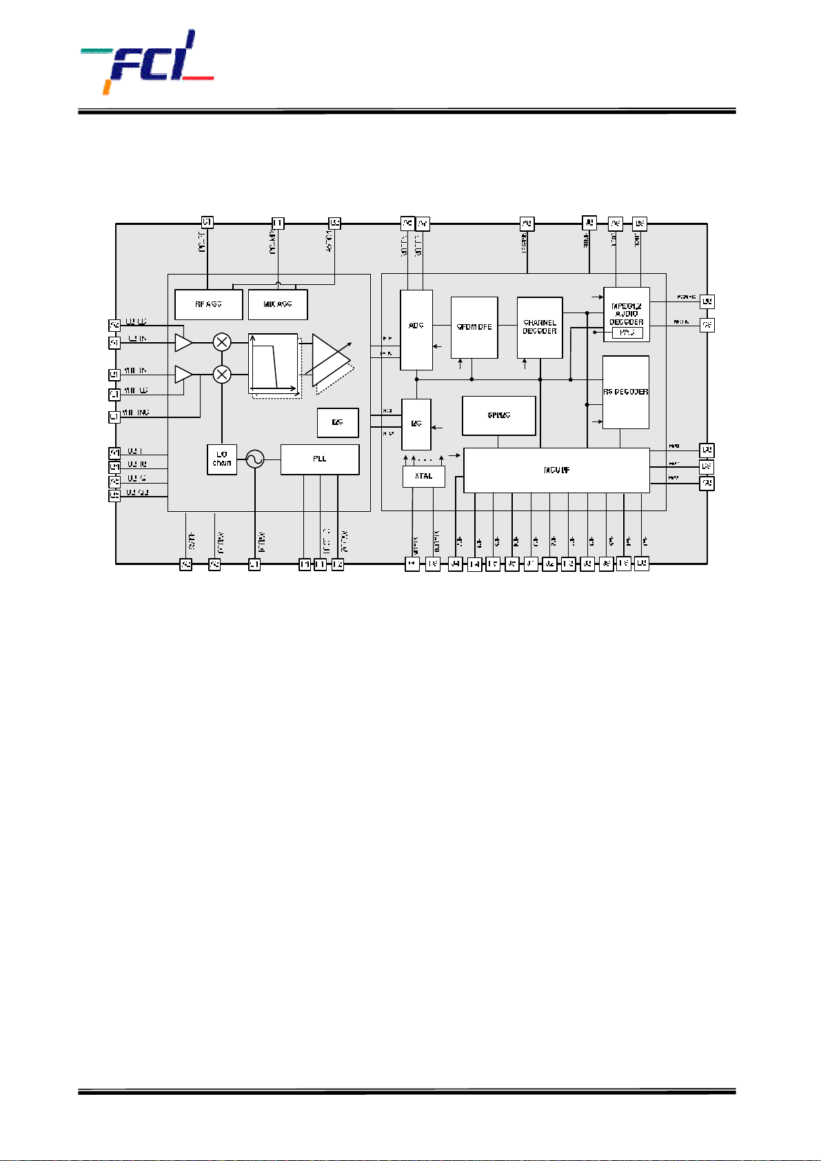
1.3. Block Diagram
Terrestrial Digital Multimedia Broadcast
RF tuner & Demodulator
1.4. RF Tuner
RF tuner has a direct-conversion structure that converts Band-3 or L-Band signal around DC
frequency. RF AGC and MIX AGC are controlled by the on-chip demodulator, and they regulate signal
level to a proper value for the internal tuner blocks. The on-chip demodulator controls the gain of
the PGA (Programmable Gain Amplifier), and PGA supply uniform signal to ADC as a result. A low
noise fractional-N type frequency synthesizer and a VCO are integrated for generating LO(Local
Oscillator) signal to direct-conversion.
Figure 1. T-DMB Block Diagram
ⓒCopyright 2008 FCI (All Rights Reserved)
Product datasheet 7/49 Rev. 18 Feb. 2009 -
Page 8

FC80
01
1.5. Functional Description
1.5.1. Frame Synchronization and Mode Detection
Frame synchronization could get the start position of a frame and transmission mode by calculating
the energy range of the sampling data.
1.5.2. Automatic Gain Control (AGC)
AGC should preserve the amplitude of received signal to uniformity automatically.
It is affected to control the level of Viterbi soft decision signal.
1.5.3. Fast Fourier Transform (FFT)
Terrestrial Digital Multimedia Broadcast
RF tuner & Demodulator
FFF transform time signal of sub-carrier to frequency signal according to DMB transmission mode.
1.5.4. QPSK Demodulator
QPSK demodulator includes differential demodulation, QPSK de-mapping and frequency deinterleaving function, etc.
1.5.5. Time de-interleaver / de-puncture
Time de-interleaver is capable of decoding 4 channels simultaneously. Also it can process
independent of channel size with adapting effective de-interleaving technique. It satisfies Eureka147 specification.
1.5.6. Viterbi Decoder/Inverse Energy Disposal Scrambler
Viterbi decoder should decode convolutional code that is adequate to mobile channel receiver.
It uses Maximum Likelihood Sequence Estimation. It is capable of decoding channel that is
RCPC code of 1/4 to 8/9 variable code rate.
1.5.7. MPEG-1,2 Audio Decoder
It satisfies MPEG-1,2 Layer II Audio specification. It is designed fully hardwired for reducing power
ⓒCopyright 2008 FCI (All Rights Reserved)
Product datasheet 8/49 Rev. 18 Feb. 2009 -
Page 9

FC80
01
consumption.
1.5.8. CODEC Interface
ü Left-Justified / Right-Justified / I2S
ü Serial Output Data : 24bit / 20bit / 16bit
ü I2S : support Master / Slave mode
ü Auto Detection for MPEG-1 (LRCK=48KHz) and MPEG-2 (LRCK=24KHz).
ü Capable of MPEG-2 output with 48KHz sampling
ü CRC error check
ü PAD data extraction and transmitting to Host
1.5.9. Convolutional De-interleaver
Terrestrial Digital Multimedia Broadcast
RF tuner & Demodulator
The function of Convolutional De-Interleaver is to transform burst error to random errot. It
should detect sync byte of 204 bytes RS frame.
1.5.10. RS Decoder
RS decoder should adapt (204, 188) shorten RS specification. It is capable of 8 byte error correction
of 204 bytes.
1.5.11. Clock Generator
The DMB Baseband Chip and peripheral clocks operate from a single 24.576MHz oscillator.
ⓒCopyright 2008 FCI (All Rights Reserved)
Product datasheet 9/49 Rev. 18 Feb. 2009 -
 Loading...