

Page 1
Future
Communications
Integrated circuit Inc.
FC7870
RF Transceiver IC for Multi-band & Multi-mode
Applications (GSM/EDGE/HSPA/HSPA+/LTE)
D
ESCRIPTION
FC7870 of FCI’s zipRF™ family is a multi-band
and multi-mode RF-to-baseband direct-conversion
transceiver IC which covers most of the 2G, 3G,
and 4G applications including GSM, GPRS, EDGE,
WCDMA, HSPA, HSPA+, TD-SCDMA, FDD and
TDD LTE. FC7870 covers almost all the frequency
allocation bands from 1 to 41 with receiver diversity.
It is a highly integrated chip working with dual
supply voltage such as 1.2V and 1.8V. Due to the
linear, wide dynamic range transmit chain with low
RX-band phase noise characteristics and low nois e
figure and highly linear receive chain, the RX and
TX RF SAW filters are no longer required in most of
the applications. The 4-wired serial-to-parallel
interface (SPI) enables FC7870 to operate in
various modes.
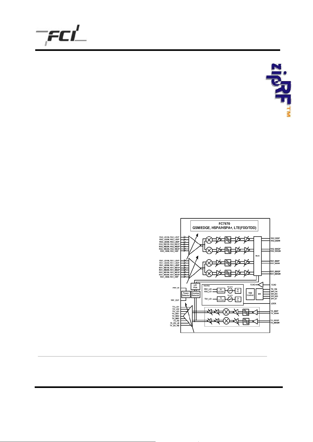
FC7870 contains complete multi-band receiver
diversity path such as LNA, down-conversion mixer,
channel selection filter (CSF), baseband
programmable gain amplifier (PGA), Rx VCO, Rx
PLL, and LO distribution block. FC7870 also
contains complete transmitter path such as
baseband amplifier, TX channel filter, up-converter,
RF programmable drive amplifier (DA), Tx VCO, Tx
PLL, RMS detector, envelop detector, and LO
distribution block. The RMS power detector is
included to indicate the received TX output power
level whereas the envelop detector is used for
internal TX DC and I/Q calibration. FC7870 is
available in 4.87mm x 4.87mm 121-pin WLCSP
(wafer level chip scale package).
FC7870 fully support all the various FDD/TDD
duplexing method. For TDD operation, the TX_ON
hardware pin exists. Also SPI controlled TDD
operation is supported. During TDD operation, RX
VCO/PLL can be configured to operate as a
common LO supporting both of the TX and RX
operation.
F
EATURES
Complete MIMO (2Rx,1Tx) transceiver with
receiver diversity covering multi-band (Band1~41)
supporting multiple standards such as
GSM/GPRS/EDGE, TD-SCDMA, WCDMA,
HSPA+, and TDD/ FDD LTE applications
Low noise and highly linear wide-band LNAs
with 8 and 7 LNAs in the primary and secondary
receive signal path.
Low Rx-band phase noise and highly linear
wide-band TX output from 9 drive amplifiers.
Fully integrated low phase noise Rx and Tx
VCO and Fractional-N PLL with fine frequency
resolution with self-calibrated VCO frequency.
Modem assisted TX LO leakage, TX I/Q, and
RX DC offset calibration
Self-calibrated RX/TX channel filter frequency
Greater than 85-dB transmitter output power
control and greater than 95-dB receiver gain
control
Modem assisted Ramping for 2G GSM/EDGE
4.87mm x 4.87mm 121-pin WLCSP package
B
LOCK DIAGRAM
A
PPLICATIONS
-
2G/3G/4G multi-band mobile phone
-
Multi-band LTE & HSPA+ mobile phone
FCI Inc.
th
Floor, Kins Tower, 25-1 Website: http://www. f ci .co.kr
11
Jeongja-Dong, Bundang-Gu, E-mail: [email protected]
Sungnam City, Gyunggi-do, Phone: 82-31-711-6444
463-811, KOREA Fax: 82-31-711-0313
FCI Confidential and Proprietary Information
1 / 26
These materials could be changed without prior notice.
Last Update Nov/03/2012
 Loading...