

Page 1

RS9116 CC1 Connectivity Module Datasheet v1.0.8, Dec-2020
RS9116 n-Link™ and WiSeConnect™ Wi-Fi® and Dual-mode Bluetooth® 5
Wireless Connectivity CC1 Module Solutions
Overview
1.1 Features
Wi-Fi
• Compliant to 1x1 IEEE 802.11 a/b/g/n with dual
band (2.4 and 5 GHz) support
• Transmit power up to +18 dBm in 2 GHz and
+13.5 dBm in 5 GHz
• Receive sensitivity as low as -96 dBm in 2 GHz
and -89 dBm in 5 GHz
• Data Rates: 802.11b: Up to 11 Mbps; 802.11g/a:
Up to 54 Mbps; 802.11n: MCS0 to MCS7
• Operating Frequency Range: 2412 MHz – 2484
MHz, 4.9 GHz – 5.975 GHz
Bluetooth
• Transmit power up to +16 dBm with integrated PA
• Receive sensitivity: LE: -92 dBm, LR 125 Kbps: -
102 dBm
• Compliant to dual-mode Bluetooth 5
• <8 mA transmit current in Bluetooth 5 mode, 2
Mbps data rate
• Data rates: 125 Kbps, 500 Kbps, 1 Mbps, 2 Mbps,
3 Mbps
• Operating Frequency Range: 2.402 GHz - 2.480
GHz
• Bluetooth 2.1 + EDR, Bluetooth Low Energy 4.0 /
4.1 / 4.2 / 5.0
• Bluetooth Low Energy 1 Mbps, 2 Mbps and Long
Range modes
• Diversity is supported
Power Consumption (2.4 GHz)
• Wi-Fi Standby Associated mode current: 102 uA
@ 1 second beacon interval
• Wi-Fi 1 Mbps Listen current: 14 mA
• Wi-Fi LP chain Rx current: 20 mA
• Deep sleep current <1 uA, Standby current (RAM
retention) < 10 uA
Operating Conditions
• Wide operating supply range: 1.75 V to 3.63 V
• Operating temperature: -40 ºC to +85 ºC (Industrial
grade)
Size
• Small Form Factor: 15 x 15.7 x 2.2 mm
Software Operating Modes
• Hosted mode (n-Link™): Wi-Fi stack, Bluetooth
stack and profiles and all network stacks reside on
the host processor
• Embedded mode (WiSeConnect™): Wi-Fi stack,
TCP/IP stack, IP modules, Bluetooth stack and
some profiles reside in RS9116; Some of the
Bluetooth profiles reside in the host processor
Hosted Mode (n-Link™)
• Available host interfaces: SDIO 2.0 and USB HS
• Support for 20 MHz channel bandwidth
• Bluetooth Low Energy Secure connections
• Bluetooth Low Energy supports central role and
peripheral role concurrently
• Bluetooth auto rate and auto TX power adaptation
• Scatternet* with two slave roles while still being
visible
RF Features
• Integrated baseband processor with calibration
memory, RF transceiver, high-power amplifier,
balun and T/R switch
• Modules with Integrated Antenna and u.FL
connector
silabs.com | Building a more connected world. Rev 1.0.8 1 | Page
PRELIMINARY | Subject to change.
• Application data throughput up to 50 Mbps (Hosted
Mode) in 802.11n with 20 MHz bandwidth
• Host drivers for Linux
• Support for Client mode, Access point mode (Up to
16 clients), Concurrent Client and Access Point
mode, and Enterprise Security
• Support for concurrent Wi-Fi, dual-mode
Bluetooth 5
Embedded Mode (WiSeConnect™)
• Available host interface: UART, SPI, and USB
CDC
Page 2

RS9116 CC1 Connectivity Module Datasheet v1.0.8, Dec-2020
silabs.com | Building a more connected world. Rev 1.0.8 2 | Page
PRELIMINARY | Subject to change.
• Support for Embedded Client mode, Access Point
mode (Up to 8 clients), Concurrent Client and
Access Point mode, and Enterprise Security
• Supports advanced security features: WPA/WPA2-
Personal and Enterprise
• Integrated TCP/IP stack, HTTP/HTTPS, SSL/TLS,
MQTT
• Bluetooth inbuilt stack support for L2CAP,
RFCOMM, SDP, SPP, GAP
• Bluetooth profile support for GAP, SDP, SPP,
GATT, L2CAP, RFCOMM
• Wireless firmware update and provisioning
• Support for concurrent Wi-Fi, dual-mode
Bluetooth 5
Security
• Accelerators: AES128/256 in Embedded Mode
• WPA/WPA2-Personal, WPA/WPA2 Enterprise for
Client
Software and Regulatory Certification
• Wi-Fi Alliance*
• Bluetooth Qualification*
• Regulatory certifications (FCC, IC, CE/ETSI,
TELEC)*
Evaluation Kit
• Dual Band EVK: RS9116X-DB-EVK1
* For a detailed list of software features and available profiles, refer to the Software Reference Manuals or
contact Silicon Labs for availability.
All power and performance numbers are under ideal conditions.
1.2 Applications
Wearables
Smart Watches, Wristbands, Fitness Monitors, Smart Glasses, etc.
Smart Home
Smart Locks, Motion/Entrance Sensors, Water Leak sensors, Smart plugs/switches, LED lights, Door-bell cameras,
Washers/Dryers, Refrigerators, Thermostats, Consumer Security cameras, Voice Assistants, etc.
Other Consumer Applications
Toys, Anti-theft tags, Smart dispensers, Weighing scales, Blood pressure monitors, Blood sugar monitors, Portable
cameras, etc.
Other Applications (Medical, Industrial, Retail, Agricultural, Smart City, etc.)
Healthcare Tags, Medical patches/pills, Infusion pumps, Sensors/actuators in Manufacturing, Electronic Shelf labels,
Agricultural sensors, Product tracking tags, Smart Meters, Parking sensors, Street LED lighting, Automotive Aftermarket, Security Cameras, etc.
1.3 Description
Silicon Labs' RS9116 dual band CC1 module provides a comprehensive multi-protocol wireless connectivity solution
including 802.11 a/b/g/n (2.4 GHz and 5 GHz), and dual-mode Bluetooth 5. The modules offer high throughput,
extended range with power-optimized performance. The modules are FCC, IC, and ETSI/CE certified.
Page 3
RS9116 CC1 Connectivity Module Datasheet v1.0.8, Dec-2020
silabs.com | Building a more connected world. Rev 1.0.8 3 | Page
PRELIMINARY | Subject to change.
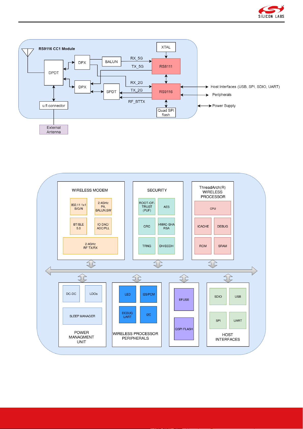
1.4 Block Diagrams
Figure 1. CC1 Module Block Diagram
Figure 2. RS9116 Connectivity Hardware Block Diagram
Page 4
RS9116 CC1 Connectivity Module Datasheet v1.0.8, Dec-2020
silabs.com | Building a more connected world. Rev 1.0.8 4 | Page
PRELIMINARY | Subject to change.
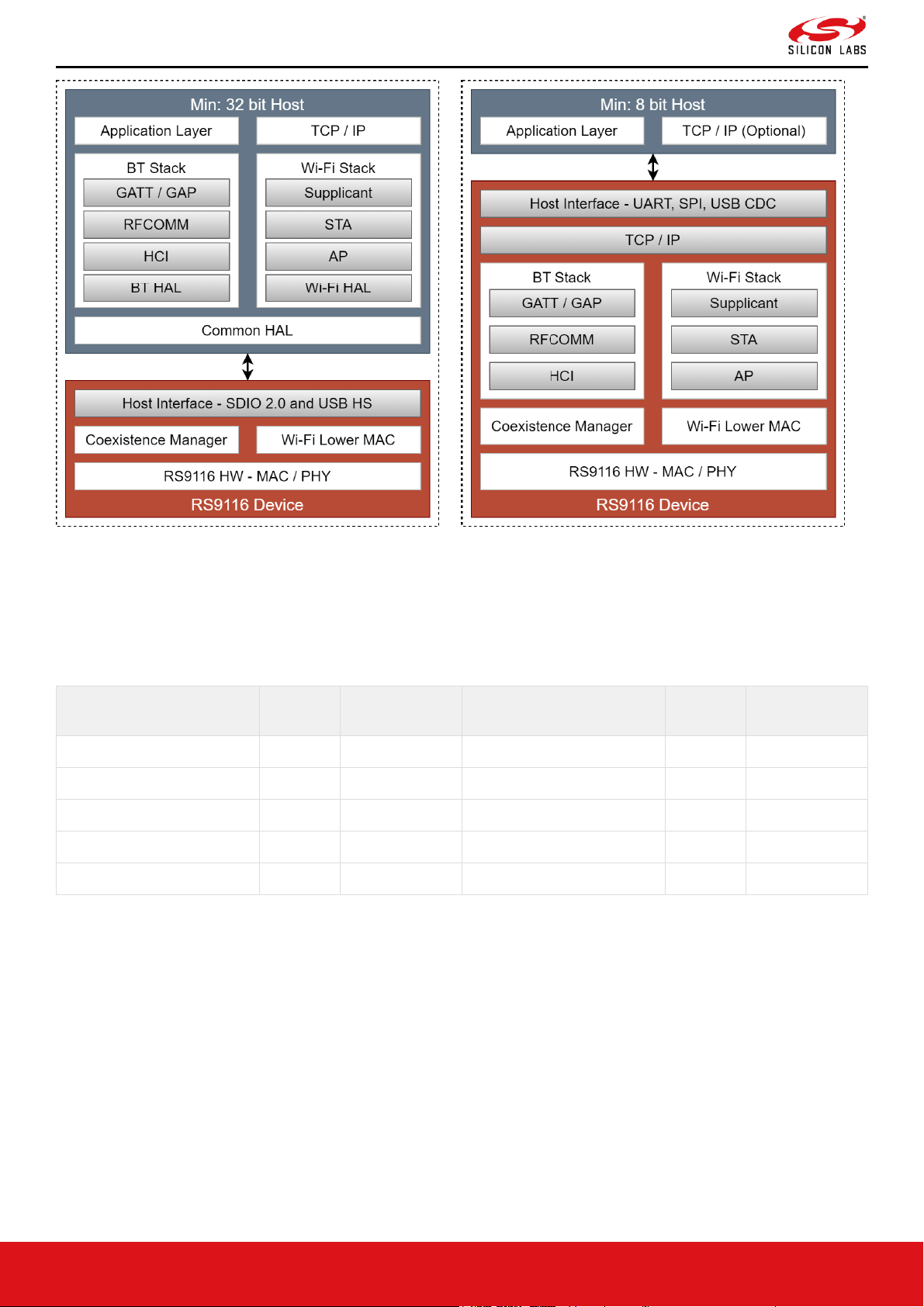
Figure 3. Hosted Software Architecture Figure 4. Embedded Software Architecture
1.5 Device Information
Part Number
Flash
Type
Package Type
Package Size
Silicon
Rev
Firmware
Version
RS9116W-DB00-CC1-X24
Internal
SIP,LGA(155)
15 mm x 15.7 mm x 2.2 mm
1.3
1.2.24
RS9116W-DB00-CC1-B24
Internal
SIP,LGA(155)
15 mm x 15.7 mm x 2.2 mm
1.4
1.2.24
RS9116W-DB00-CC1-B2A
Internal
SIP,LGA(155)
15 mm x 15.7 mm x 2.2 mm
1.4
2.0
RS9116N-DB00-CC1-X00
Internal
SIP,LGA(155)
15 mm x 15.7 mm x 2.2 mm
1.3
Not Applicable
RS9116N-DB00-CC1-B00
Internal
SIP,LGA(155)
15 mm x 15.7 mm x 2.2 mm
1.4
Not Applicable
Page 5

RS9116 CC1 Connectivity Module Datasheet v1.0.8, Dec-2020
silabs.com | Building a more connected world. Rev 1.0.8 5 | Page
PRELIMINARY | Subject to change.
Table of Contents
1 Overview ................................................................................................................................................................... 1
1.1 Features ................................................................................................................................................................. 1
1.2 Applications ............................................................................................................................................................ 2
1.3 Description ............................................................................................................................................................. 2
1.4 Block Diagrams ...................................................................................................................................................... 3
1.5 Device Information ................................................................................................................................................. 4
2 RS9116 CC1 Module Pinout and Pin Description ................................................................................................. 7
2.1 Pin Diagram ............................................................................................................................................................ 7
2.2 Pin Description ....................................................................................................................................................... 8
2.2.1 RF & Control Interfaces ....................................................................................................................................................... 8
2.2.2 Power & Ground Pins .......................................................................................................................................................... 8
2.2.3 Host & Peripheral Interfaces ................................................................................................................................................ 9
2.2.4 Miscellaneous Pins ............................................................................................................................................................ 22
3 RS9116 CC1 Module Specifications ..................................................................................................................... 23
3.1 Absolute Maximum Ratings.................................................................................................................................. 23
3.2 Recommended Operating Conditions .................................................................................................................. 24
3.3 DC Characteristics ............................................................................................................................................... 25
3.3.1 Reset Pin ........................................................................................................................................................................... 25
3.3.2 Power Sequence ............................................................................................................................................................... 26
3.3.3 Digital Input Output Signals ............................................................................................................................................... 30
3.3.4 USB ................................................................................................................................................................................... 30
3.3.5 Pin Capacitances ............................................................................................................................................................... 30
3.4 AC Characteristics ................................................................................................................................................ 30
3.4.1 Clock Specifications .......................................................................................................................................................... 30
3.4.2 SDIO 2.0 Slave .................................................................................................................................................................. 32
3.4.3 SPI Slave ........................................................................................................................................................................... 33
3.4.4 USB ................................................................................................................................................................................... 35
3.4.5 UART ................................................................................................................................................................................. 36
3.4.6 I2C Master and Slave ........................................................................................................................................................ 36
3.4.7 I2S/PCM Master and Slave ............................................................................................................................................... 37
3.4.8 GPIO pins .......................................................................................................................................................................... 38
3.5 RF Characteristics ................................................................................................................................................ 39
3.5.1 WLAN 2.4 GHz Transmitter Characteristics ...................................................................................................................... 39
3.5.2 WLAN 2.4 GHz Receiver Characteristics on High-Performance (HP) RF Chain ............................................................... 41
3.5.3 WLAN 2.4 GHz Receiver Characteristics on Low-Power (LP) RF Chain ........................................................................... 42
3.5.4 Bluetooth Transmitter Characteristics on High-Performance (HP) RF Chain .................................................................... 44
3.5.5 Bluetooth Transmitter Characteristics on Low-Power (LP) 0 dBm RF Chain ..................................................................... 45
3.5.6 Bluetooth Receiver Characteristics on High-Performance (HP) RF Chain ........................................................................ 46
3.5.7 Bluetooth Receiver Characteristics on Low-Power (LP) RF Chain .................................................................................... 49
3.5.8 WLAN 5GHz Transmitter Characteristics .......................................................................................................................... 51
3.5.9 WLAN 5GHz Receiver Characteristics .............................................................................................................................. 53
3.6 Typical Current Consumption ............................................................................................................................... 56
3.6.1 3.3 V .................................................................................................................................................................................. 56
4 RS9116 CC1 Module Detailed Description .......................................................................................................... 59
4.1 Overview............................................................................................................................................................... 59
4.2 Module Features .................................................................................................................................................. 59
4.2.1 WLAN ................................................................................................................................................................................ 59
4.2.2 Bluetooth ........................................................................................................................................................................... 59
4.2.3 RF Transceiver .................................................................................................................................................................. 61
4.2.4 Host Interfaces .................................................................................................................................................................. 61
4.2.5 Wireless Coexistence Manager ......................................................................................................................................... 61
4.2.6 Software ............................................................................................................................................................................ 61
4.2.7 Security ............................................................................................................................................................................. 62
4.2.8 Power Management .......................................................................................................................................................... 63
4.2.9 Low power modes ............................................................................................................................................................. 63
4.2.10 Memory ............................................................................................................................................................................. 64
5 RS9116 CC1 Module Reference Schematics, BOM and Layout Guidelines .................................................... 65
5.1 SDIO/SPI/UART ................................................................................................................................................... 65
5.1.1 Schematics ........................................................................................................................................................................ 65
5.1.2 Bill of Materials .................................................................................................................................................................. 67
5.2 USB/USB-CDC ..................................................................................................................................................... 68
5.2.1 Schematics ........................................................................................................................................................................ 68
5.2.2 Bill of Materials .................................................................................................................................................................. 70
Page 6

RS9116 CC1 Connectivity Module Datasheet v1.0.8, Dec-2020
silabs.com | Building a more connected world. Rev 1.0.8 6 | Page
PRELIMINARY | Subject to change.
5.3 Layout Guidelines ................................................................................................................................................. 71
6 RS9116 CC1 Module Antenna Specifications ..................................................................................................... 75
6.1 Overview............................................................................................................................................................... 75
6.2 PCB Antenna Performance Specifications ........................................................................................................... 75
6.2.1 Return Loss Characteristic of the Antenna ........................................................................................................................ 75
6.2.2 Module Reference Orientation ........................................................................................................................................... 75
6.2.3 2D Gain Plots at 2.4 GHz .................................................................................................................................................. 76
6.2.4 2D Gain Plots at 2.430 GHz .............................................................................................................................................. 78
6.2.5 2D Gain Plots at 2.480 GHz .............................................................................................................................................. 79
6.2.6 2D Gain Plots at 5.1 GHz .................................................................................................................................................. 81
6.2.7 2D Gain Plots at 5.5 GHz .................................................................................................................................................. 82
6.2.8 2D Gain Plots at 5.9 GHz .................................................................................................................................................. 84
6.3 Antenna Parameters ............................................................................................................................................ 85
6.4 Mechanical Characteristics .................................................................................................................................. 85
7 RS9116 CC1 Module Storage, Handling and Soldering Conditions ................................................................. 86
7.1 Recommended Reflow Profile .............................................................................................................................. 86
7.2 Baking Instructions ............................................................................................................................................... 86
8 RS9116 CC1 Module Package Description.......................................................................................................... 87
8.1 Dimensions ........................................................................................................................................................... 87
8.1.1 Packing Information of Modules with Package Codes CC1 ............................................................................................... 87
8.2 Package Outline ................................................................................................................................................... 88
8.3 PCB Landing Pattern ............................................................................................................................................ 89
9 RS9116 CC1 Module Certification and Ordering Information ........................................................................... 90
9.1 Certification Information ....................................................................................................................................... 90
9.2 Compliance and Certification ............................................................................................................................... 90
9.2.1 Federal Communication Commission Statement ............................................................................................................... 90
9.2.2 Industry Canada / ISED Statement .................................................................................................................................... 91
9.2.3 CE ..................................................................................................................................................................................... 92
9.2.4 TELEC ............................................................................................................................................................................... 92
9.2.5 Qualified Antenna Types ................................................................................................................................................... 92
9.2.6 Module Marking Information .............................................................................................................................................. 93
9.3 Module Package ................................................................................................................................................... 94
9.4 Ordering Information ............................................................................................................................................ 94
9.4.1 Device Nomenclature ........................................................................................................................................................ 95
10 RS9116 CC1 Module Documentation and Support ......................................................................................... 96
10.1 Resource Location ............................................................................................................................................ 96
11 RS9116 CC1 Module Revision History ............................................................................................................. 97
Page 7

RS9116 CC1 Connectivity Module Datasheet v1.0.8, Dec-2020
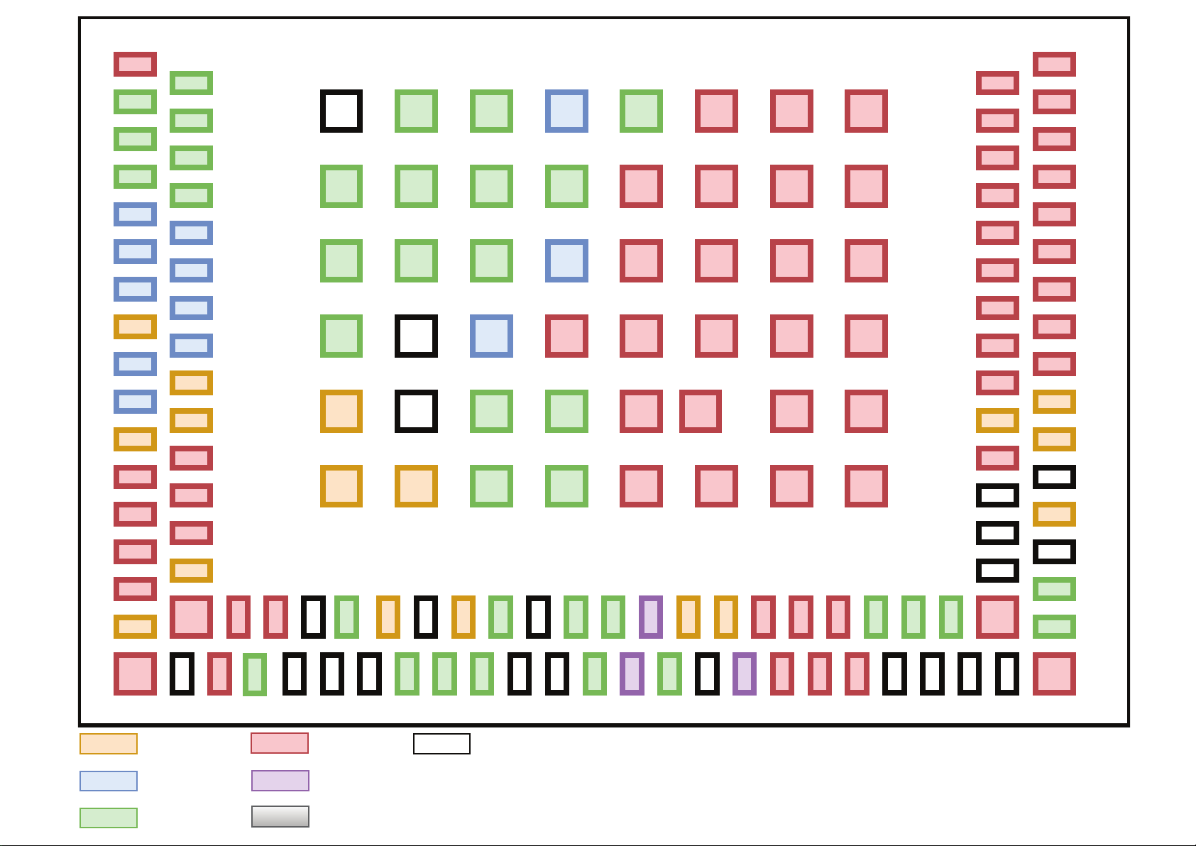
2 RS9116 CC1 Module Pinout and Pin Description
2.1 Pin Diagram
silabs.com | Building a more connected world. Rev 1.0.8 7 | Page
PRELIMINARY | Subject to change.
Page 8
GND
GPIO_51
GPIO_49
GPIO_47
SDIO_CLK/
SPI_CLK
SDIO_D0/
SPI_MOSI
SDIO_D2
/
SPI_INTR
SDIO_IO_VDD
USB_DP
USB_VBUS
USB_AVDD_1P1
GND
GND
GND
GND
VOUTLDOSOC
NC
GPIO_50
GPIO_46
GPIO_48
GPIO_15
SDIO_CMD/
SPI_CSN
SDIO_D1/
SPI_MISO
SDIO_D3/
SP
USB_CDC_DIS
USB_DM
USB_AVDD_3P3
UULP_VBATT_1
GND
GND
GND
VIN_3P3
GND
GNDNCNCNCNCNCJP0
NC
RESET_N
GND
GND
GND
GNDNCNCNCNC
GND
GND
GNDNCNCNCJP2
GND
GND
GND
GND
GND
GND
GND
GND
GND
GND
GND
GND
GND
RF_AVDD_BTTX
PA5G_AVDD
NC
AVDD_1P9_3P3
NC
UULP_VBAT_GPIO_3
ULP_GPIO_10
GND
GND
GND
GND
GND
GND
GND
GND
GND
VOUTLDOAFE
GND
NC
NC
NC
NC
GPIO_11
GPIO_6
UART1_TX
UULP_VBAT_GPIO_4
GND
GND
GND
GPIO_54
GPIO_52
GPIO_10
GPIO_12
GND
GND
GND
GND
GPIO_56
GPIO_55
GPIO_53
UART1_RX
GND
GND
GND
GND
GPIO_57NCUSB_ID
GND
GND
GND
GND
GND
ULP_IO_VDDNCGPIO_38
GPIO_7
GND
GND
GND
GND
VOUTLDO1P8
UULP_AVDD
JNC
JP1
GND
GND
GND
GND
1
3
2
4
6
5
7
9
8
10
11
13
15
14
16
17
58
60
59
61
63
62
64
66
65
67
69
68
70
71
72
57
55
56
54
52
53
51
49
50
48
47
45
43
44
42
41
107
105
106
104
102
103
101
100
999897
96
95
94
93
18
19
20212223242526
27
28
293031
323334
35
36
37
383940
737475
76
77
78
798081
82
83
8485868788
89
90
91
92
108
109
110
111
112
113
114
115
116
117
118
119
120
121
122
123
124
125
126
127
128
129
130
131
132
133
134
135
136
137
138
139
140
141
142
143
144
145
146
147
148
149
150
151
152
153
154
155
ULP_GPIO_0
ULP_GPIO_5
UULP_VOUTSCDC
POC_OUT
AVDD_1P2
RF_AVDD33
46
12
I_ERR_INTR/
_RETN
Power Supplies
Host
GPIO & Peripherals
Grounds
RF & Control
Miscellaneous
NC
Figure 5. RS9116 CC1 Pin Diagram
Page 9
RS9116 CC1 Connectivity Module Datasheet v1.0.8, Dec-2020
silabs.com | Building a more connected world. Rev 1.0.8 8 | Page
PRELIMINARY | Subject to change.
2.2 Pin Description
2.2.1 RF & Control Interfaces
Pin Name
Pin Number
I/O Supply Domain
Direction
Initial State (Power up,
Active Reset)
Description
RESET_N
33
UULP_VBATT_1
Input
NA
Active-low reset asynchronous reset
signal
POC_IN
30
UULP_VBATT_1
Input
NA
Power On Control Input
POC_OUT
84
UULP_VBATT_1
Ouput
NA
Power On Control Output
Table 1. RF & Control Interfaces
2.2.2 Power & Ground Pins
Pin Name
Type
Pin Number
Direction
Description
UULP_VBATT_1
Power
67
Input
Always-on VBATT Power supply to the UULP domains
VIN_3P3
Power
71
Input
Digital Power Supply
VOUTLDOSOC
Power
16
Output
Output of SoC LDO
VOUTLDO1P8
Power
108
Output
Output of 1.8V LDO
VOUTLDOAFE
Power
98
Output
Output of AFE LDO
SDIO_IO_VDD
Power
8
Input
I/O Supply for SDIO I/Os. Refer to the GPIOs section for details on
which GPIOs have this as the I/O supply.
ULP_IO_VDD
Power
116
Input
I/O Supply for ULP GPIOs
PA5G_AVDD
Power
47
Input
Power supply for the 5 GHz RF Power Amplifier
RF_AVDD_BTTX
Power
48
Input
Power supply for Bluetooth Transmit circuit.Connect to
VOUTLDOAFE as per the Reference Schematics.
RF_AVDD33
Power
86
Input
Power supply for the 5 GHz RF
AVDD_1P9_3P3
Power
45
Input
Power supply for the 5 GHz RF
Page 10
RS9116 CC1 Connectivity Module Datasheet v1.0.8, Dec-2020
silabs.com | Building a more connected world. Rev 1.0.8 9 | Page
PRELIMINARY | Subject to change.
Pin Name
Type
Pin Number
Direction
Description
AVDD_1P2
Power
85
Input
Power supply for the 5 GHz RF. Connect to VOUTLDOSOC as per
the Reference Schematics.
UULP_VOUTSCDC
Power
79
Output
UULP Switched Cap DCDC Output
UULP_VOUTSCDC_RE
TN
Power
77
Output
UULP Retention Supply Output
UULP_AVDD
Power
109
Input
Power supply for the always-on digital and ULP peripherals.Connect
to UULP_VOUTSCDC as per the Reference Schematics.
USB_AVDD_3P3
Power
66
Input
Power Supply for the USB interface
USB_AVDD_1P1
Power
11
Input
Power supply for the USB core
GND
Ground
1, 12, 13, 14, 15, 17, 19,
34, 35, 36, 41, 49, 50,
51, 52, 53, 54, 55, 56,
57, 68, 69, 70, 72, 73,
74, 87, 88, 89, 93, 97,
99, 100, 101, 102, 103,
104, 105, 106, 107, 112,
113, 114, 115, 120, 121,
122, 123, 127, 128, 129,
130, 131, 136, 137, 138,
139, 144, 145, 146, 147,
153, 154, 155
GND
Common ground pins
Table 2. Power and Ground Pins
2.2.3 Host & Peripheral Interfaces
Pin Name
Pin Number
I/O Supply Domain
Direction
Initial State (Power up,
Active Reset)
Description
1,2,3,4
GPIO_6
150
VIN_3P3
Inout
HighZ
Default : HighZ
Sleep: HighZ
This pin can be configured by software to
be any of the following
• I2S_DOUT - I2S interface output data.
Page 11

RS9116 CC1 Connectivity Module Datasheet v1.0.8, Dec-2020
silabs.com | Building a more connected world. Rev 1.0.8 10 | Page
PRELIMINARY | Subject to change.
Pin Name
Pin Number
I/O Supply Domain
Direction
Initial State (Power up,
Active Reset)
Description
1,2,3,4
• PCM_DOUT - PCM interface output
data.
GPIO_7
119
VIN_3P3
Inout
HighZ
Default : HighZ
Sleep: HighZ
This pin can be configured by software to
be any of the following
• I2S_CLK - I2S interface clock.
• PCM_CLK - PCM interface clock.
UART1_RX
135
VIN_3P3
Inout
HighZ
Host
Default
Sleep
UART
UART1_RX
- UART Host
interface
serial input.
HighZ
Non UART
HighZ
HighZ
The UART interface is supported only in
WiSeConnect™.
UART1_TX
151
VIN_3P3
Inout
HighZ
Host
Default
Sleep
UART
UART1_TX UART Host
interface
serial
output.
HighZ
Non UART
HighZ
HighZ
The UART interface is supported only in
WiSeConnect™.
GPIO_10
142
VIN_3P3
Inout
HighZ
Default : HighZ
Sleep: HighZ
Page 12
RS9116 CC1 Connectivity Module Datasheet v1.0.8, Dec-2020
silabs.com | Building a more connected world. Rev 1.0.8 11 | Page
PRELIMINARY | Subject to change.
Pin Name
Pin Number
I/O Supply Domain
Direction
Initial State (Power up,
Active Reset)
Description
1,2,3,4
This pin can be configured by software to
be any of the following
• I2S_DIN: I2S interface input data.
• PCM_DIN - PCM interface input data.
GPIO_11
149
VIN_3P3
Inout
HighZ
Default : HighZ.
Sleep: HighZ
This pin can be configured by software to
be any of the following
• I2S_WS: I2S interface Word Select.
• PCM_FSYNC: PCM interface Frame
Synchronization signal.
GPIO_12
143
VIN_3P3
Inout
HighZ
Default : HighZ
Sleep: HighZ
This pin can be configured by software to
be any of the following
• UART1_RTS - UART interface
Request to Send, if UART Host
Interface flow control is enabled.
The UART interface is supported only in
WiSeConnect™.
GPIO_15
61
VIN_3P3
Inout
HighZ
Default : HighZ
Sleep: HighZ
This pin can be configured by software to
be any of the following
• UART1_CTS - UART interface Clear
to Send, if UART Host Interface flow
control is enabled.
• UART1_TRANSPARENT_MODE -
UART Host interface Transparent
Mode, Indication that module has
Page 13

RS9116 CC1 Connectivity Module Datasheet v1.0.8, Dec-2020
silabs.com | Building a more connected world. Rev 1.0.8 12 | Page
PRELIMINARY | Subject to change.
Pin Name
Pin Number
I/O Supply Domain
Direction
Initial State (Power up,
Active Reset)
Description
1,2,3,4
entered into TRANSPERENT_MODE
• TSF_SYNC - Transmit
Synchronization Function signal to
indicate to the Host when a packet is
transmitted. The signal is toggled once
at the end of every transmitted packet.
The UART interface is supported only in
WiSeConnect™.
SDIO_CLK/SPI_CLK
5
SDIO_IO_VDD
Inout
HighZ
Host
Default
Sleep
SDIO
SDIO_CLK SDIO
interface
clock
HighZ
SPI
SPI_CLK SPI Slave
interface
clock
HighZ
Non
SDIO,SPI
HighZ
HighZ
The SPI interface is supported only in
WiSeConnect™.
SDIO_CMD/SPI_CSN
62
SDIO_IO_VDD
Inout
HighZ
Host
Default
Sleep
SDIO
SDIO_CMD
- SDIO
interface
CMD signal
HighZ
SPI
SPI_CSN Active-low
Chip Select
signal of SPI
HighZ
Page 14

RS9116 CC1 Connectivity Module Datasheet v1.0.8, Dec-2020
silabs.com | Building a more connected world. Rev 1.0.8 13 | Page
PRELIMINARY | Subject to change.
Pin Name
Pin Number
I/O Supply Domain
Direction
Initial State (Power up,
Active Reset)
Description
1,2,3,4
Slave
interface
Non
SDIO,SPI
HighZ
HighZ
The SPI interface is supported only in
WiSeConnect™.
SDIO_D0/SPI_MOSI
6
SDIO_IO_VDD
Inout
HighZ
Host
Default
Sleep
SDIO
SDIO_D0 SDIO
interface
Data0 signal
HighZ
SPI
SPI_MOSI SPI Slave
interface
Master-OutSlave-In
signal
HighZ
Non
SDIO,SPI
HighZ
HighZ
The SPI interface is supported only in
WiSeConnect™.
SDIO_D1/SPI_MISO
63
SDIO_IO_VDD
Inout
HighZ
Host
Default
Sleep
SDIO
SDIO_D1 SDIO
interface
Data1 signal
HighZ
SPI
SPI_MISO SPI Slave
interface
Master-In-
HighZ
Page 15

RS9116 CC1 Connectivity Module Datasheet v1.0.8, Dec-2020
silabs.com | Building a more connected world. Rev 1.0.8 14 | Page
PRELIMINARY | Subject to change.
Pin Name
Pin Number
I/O Supply Domain
Direction
Initial State (Power up,
Active Reset)
Description
1,2,3,4
Slave-Out
signal
Non
SDIO,SPI
HighZ
HighZ
The SPI interface is supported only in
WiSeConnect™.
SDIO_D2/SPI_INTR
7
SDIO_IO_VDD
Inout
HighZ
Host
Default
Sleep
SDIO
SDIO_D2 SDIO
interface
Data2 signal
HighZ
SPI
SPI_INTR SPI Slave
interface
Interrupt
Signal to the
Host
HighZ
Non
SDIO,SPI
HighZ
HighZ
The SPI interface is supported only in
WiSeConnect™.
SDIO_D3/SPI_ERR_INT
R/USB_CDC_DIS
64
SDIO_IO_VDD
Inout
Pullup
Host
Default
Sleep
SDIO
SDIO_D3 SDIO
interface
Data3 signal
HighZ
SPI
SPI_ERR_I
NTR - SPI
Bus Error
Interrupt
Signals
HighZ
Page 16

RS9116 CC1 Connectivity Module Datasheet v1.0.8, Dec-2020
silabs.com | Building a more connected world. Rev 1.0.8 15 | Page
PRELIMINARY | Subject to change.
Pin Name
Pin Number
I/O Supply Domain
Direction
Initial State (Power up,
Active Reset)
Description
1,2,3,4
USB
USB_CDC_
DIS - USBCDC ActiveHigh Disable
Signal
HighZ
Non
SDIO,SPI
HighZ
HighZ
The SPI interface is supported only in
WiSeConnect™.
GPIO_38
118
VIN_3P3
Inout
HighZ
Default : HighZ
Sleep: HighZ
GPIO_46
59
VIN_3P3
Inout
HighZ
Default : HighZ
Sleep: HighZ
GPIO_47
4
VIN_3P3
Inout
HighZ
Default : HighZ
Sleep: HighZ
GPIO_48
60
VIN_3P3
Inout
HighZ
Default : HighZ
Sleep: HighZ
GPIO_49
3
VIN_3P3
Inout
HighZ
Default : HighZ
Sleep: HighZ
GPIO_50
58
VIN_3P3
Inout
HighZ
Default : HighZ
Sleep: HighZ
GPIO_51
2
VIN_3P3
Inout
HighZ
Default : HighZ
Sleep: HighZ
GPIO_52
141
VIN_3P3
Inout
HighZ
Default : HighZ
Sleep: HighZ
GPIO_53
134
VIN_3P3
Inout
HighZ
Default : HighZ
Page 17

RS9116 CC1 Connectivity Module Datasheet v1.0.8, Dec-2020
silabs.com | Building a more connected world. Rev 1.0.8 16 | Page
PRELIMINARY | Subject to change.
Pin Name
Pin Number
I/O Supply Domain
Direction
Initial State (Power up,
Active Reset)
Description
1,2,3,4
Sleep: HighZ
GPIO_54
140
VIN_3P3
Inout
HighZ
Default : HighZ
Sleep: HighZ
GPIO_55
133
VIN_3P3
Inout
HighZ
Default : HighZ
Sleep: HighZ
GPIO_56
132
VIN_3P3
Inout
HighZ
Default : HighZ
Sleep: HighZ
GPIO_57
124
VIN_3P3
Inout
HighZ
Default : HighZ
Sleep: HighZ
ULP_GPIO_0
25
VIN_3P3
Inout
HighZ
Default : HighZ
Sleep: HighZ
This pin can be configured by software to
be any of the following
• WLAN_ACTIVE*: Active-High signal to
indicate to an external Bluetooth IC
that WLAN transmission is active. Part
of the 3-wire coexistence interface.
*This pin is intended to act as
WLAN_ACTIVE for wireless coexistence.
Please contact Silicon Labs to learn about
availability of this feature.
ULP_GPIO_1
76
VIN_3P3
Inout
HighZ
Default : HighZ
Sleep: HighZ
This pin can be configured by software to
be any of the following
• BT_ACTIVE*: Active-High signal from
an external Bluetooth IC that it is
transmitting. Part of the 3-wire
coexistence interface.
Page 18

RS9116 CC1 Connectivity Module Datasheet v1.0.8, Dec-2020
silabs.com | Building a more connected world. Rev 1.0.8 17 | Page
PRELIMINARY | Subject to change.
Pin Name
Pin Number
I/O Supply Domain
Direction
Initial State (Power up,
Active Reset)
Description
1,2,3,4
*This pin is intended to act as BT_ACTIVE
for Bluetooth coexistence. Please contact
Silicon Labs to learn about availability of
this feature.
ULP_GPIO_4
26
VIN_3P3
Inout
HighZ
Default : HighZ
ULP_GPIO_5
90
VIN_3P3
Inout
HighZ
Default : LP_WAKEUP_IN This is LP
Powersave Wakeup indication from
Device
Sleep: HighZ
This pin can be configured by software to
be any of the following
• LP_WAKEUP_IN :This is LP
Powersave Wakeup indication to
Device from HOST
• HOST_WAKEUP_INDICATION : This
is used as indication from Host to dev
that host is ready to take the packet
and Device can transfer the packet to
host. This is supported only in UART
host mode.
The UART interface is supported only
in WiSeConnect™.
ULP_GPIO_6
20
VIN_3P3
Inout
HighZ
Default : HighZ
Sleep: HighZ
This pin can be configured by software to
be any of the following
• WAKEUP_FROM_Dev* - Used as a
wakeup indication to host from device
• BT_PRIORITY**: Active-high signal
from an external Bluetooth IC that
indicates that the Bluetooth
transmissions are a higher priority.
Page 19

RS9116 CC1 Connectivity Module Datasheet v1.0.8, Dec-2020
silabs.com | Building a more connected world. Rev 1.0.8 18 | Page
PRELIMINARY | Subject to change.
Pin Name
Pin Number
I/O Supply Domain
Direction
Initial State (Power up,
Active Reset)
Description
1,2,3,4
*For Wake-on-Wireless feature this pin
needs to have a weak pull up resistor
externally.
**This pin is intended to act as
BT_PRIORITY for Bluetooth coexistence.
Please contact Silicon Labs to learn about
availability of this feature.
ULP_GPIO_7
24
VIN_3P3
Inout
HighZ
Default : HighZ
ULP_GPIO_8
80
VIN_3P3
Inout
HighZ
Default : HighZ
Sleep: HighZ
This pin can be configured by software to
be any of the following
• LED0: Control signal to an external
LED.
• (* LED0 functionality currently not
available in WiSeConnect™ modules)
UART2_TX
91
VIN_3P3
Inout
HighZ
Default : UART2_TX- Debug UART
Interface serial output
Sleep: HighZ
UART2_TX : Debug UART interface serial
output.
ULP_GPIO_10
42
VIN_3P3
Inout
HighZ
Default : HighZ
Sleep: HighZ
This pin can be configured by software to
be any of the following
• I2C_SCL: I2C interface clock.
ULP_GPIO_11
31
VIN_3P3
Inout
HighZ
Default : HighZ
Sleep: HighZ
Page 20

RS9116 CC1 Connectivity Module Datasheet v1.0.8, Dec-2020
silabs.com | Building a more connected world. Rev 1.0.8 19 | Page
PRELIMINARY | Subject to change.
Pin Name
Pin Number
I/O Supply Domain
Direction
Initial State (Power up,
Active Reset)
Description
1,2,3,4
This pin can be configured by software to
be any of the following
• I2C_SDA: I2C interface data.
UULP_VBAT_GPIO_0
83
UULP_VBATT_1
Output
High
Default : EXT_PG_EN
Sleep: SLEEP_IND_FROM_DEV /
EXT_PG_EN
This pin can be configured by software to
be any of the following
• SLEEP_IND_FROM_DEV: This signal
is used to send an indication to the
Host processor. An indication is sent
when the chip enters (logic low) and
exits (logic high) the ULP Sleep mode.
• EXT_PG_EN: Active-high enable
signal to an external power gate which
can be used to control the power
supplies other than Always-ON
VBATT Power Supplies in ULP Sleep
mode.
HOST_BYP_ULP_WAK
EUP
92
UULP_VBATT_1
Input
HighZ
Default : HOST_BYP
Sleep: ULP_WAKEUP
This signal has two functionalities – one
during the bootloading process and one
after the bootloading. During bootloading,
this signal is an active-high input to
indicate that the bootloader should bypass
any inputs from the Host processor and
continue to load the default firmware from
Flash. After bootloading, this signal is an
active-high input to indicate that the
module should wakeup from its Ultra Low
Power (ULP) sleep mode. The bootloader
bypass functionality is supported only in
WiSeConnect™.
Page 21

RS9116 CC1 Connectivity Module Datasheet v1.0.8, Dec-2020
silabs.com | Building a more connected world. Rev 1.0.8 20 | Page
PRELIMINARY | Subject to change.
Pin Name
Pin Number
I/O Supply Domain
Direction
Initial State (Power up,
Active Reset)
Description
1,2,3,4
UULP_VBAT_GPIO_3
43
UULP_VBATT_1
Inout
HighZ
Default : HighZ
Sleep: XTAL_32KHZ_IN
/ SLEEP_IND_FROM_DEV
This pin can be configured by software to
be any of the following
• XTAL_32KHZ_IN: This pin can be
used to feed external clock from a
host processor or from external crystal
oscillator.
• SLEEP_IND_FROM_DEV: This signal
is used to send an indication to the
Host processor. An indication is sent
when the chip enters (logic low) and
exits (logic high) the ULP Sleep mode.
UULP_VBAT_GPIO_4
152
UULP_VBATT_1
Inout
HighZ
Default : HighZ
Sleep: HighZ
This pin can be configured by software to
be any of the following
• XTAL_32KHZ_IN: This pin can be
used to feed external clock from a
host processor or from external crystal
oscillator.
JP0
29
VIN_3P3
Input
Pullup
Default : JP0
Sleep: HighZ
JP0 - Reserved. Connect to a test point for
debug purposes.
JP1
111
VIN_3P3
Input
Pullup
Default : JP1
Sleep: HighZ
JP1 - Reserved. Connect to a test point for
debug purposes.
JP2
82
VIN_3P3
Input
Pullup
Default : JP2
Page 22

RS9116 CC1 Connectivity Module Datasheet v1.0.8, Dec-2020
Pin Name
Pin Number
I/O Supply Domain
Direction
Initial State (Power up,
Active Reset)
Description
1,2,3,4
Sleep: HighZ
JP2 - Reserved. Connect to a test point for
debug purposes.
JNC
110
VIN_3P3
NC
Pullup
Default : JNC
Sleep: HighZ
JNC - Reserved. Connect to a test point
for debug purposes.
USB_DP
9
USB_AVDD_3P3
Inout
NA
Positive data channel from the USB
connector.
USB_DM
65
USB_AVDD_3P3
Inout
NA
Negative data channel from the USB
connector.
USB_ID
126
USB_AVDD_3P3
Input
NA
ID signal from the USB connector.
USB_VBUS
10
USB_AVDD_3P3
Input
NA
5V USB VBUS signal from the USB
connector
Table 3. Host and Peripheral Interfaces
1. "Default" state refers to the state of the device after initial boot loading and firmware loading is complete.
2. "Sleep" state refers to the state of the device after entering Sleep state which is indicated by Active-High "SLEEP_IND_FROM_DEV" signal.
3. Please refer to "RS9116N Open Source Driver Technical Reference Manual" for software programming information in hosted mode.
4. Please refer to "RS9116W SAPI Programming Reference Manual" for software programming information in embedded mode.
5. There are some functionalities, such as SLEEP_IND_FROM_DEV, that are available on multiple pins. However, these pins have other multiplexed functionalities.
Any pin can be used based on the required functionality. Customer has to note the default states before using appropriate pin.
silabs.com | Building a more connected world. Rev 1.0.8 21 | Page
PRELIMINARY | Subject to change.
Page 23

RS9116 CC1 Connectivity Module Datasheet v1.0.8, Dec-2020
silabs.com | Building a more connected world. Rev 1.0.8 22 | Page
PRELIMINARY | Subject to change.
2.2.4 Miscellaneous Pins
Pin Name
Pin Number
I/O Supply Domain
Direction
Initial State (Power up,
Active Reset)
Description
NC
18,21, 22, 23, 27, 28, 32.
37, 38, 39, 40, 44, 46,
75, 78, 81, 94, 95, 96,
117, 148, 125
NA
NA
NA
No connect.
Table 4. Miscellaneous Pins
Page 24
RS9116 CC1 Connectivity Module Datasheet v1.0.8, Dec-2020
silabs.com | Building a more connected world. Rev 1.0.8 23 | Page
PRELIMINARY | Subject to change.
3 RS9116 CC1 Module Specifications
3.1 Absolute Maximum Ratings
Functional operation above maximum ratings is not guaranteed and may damage the device. Exposure to maximum
rating conditions for extended periods may affect device reliability.
Symbol
Parameter
Min
Max
Units
T
store
Storage temperature
-40
+125 oC
T
j(max)
Maximum junction temperature
-
+125 oC
UULP_VBATT_1
Always-on VBATT supply to the UULP
Domains
-0.5
3.63
V
UULP_VBATT_2
Always-on VBATT supply to the UULP
Domains
-0.6
3.63
V
RF_VBATT
Always-on VBATT Power supply to the RF
-0.5
3.63
V
VINBCKDC
Power supply for the on-chip Buck
-0.5
3.63
V
VINLDOSOC
Power supply for SoC LDO
-0.5
1.8
V
IO_VDD_1
I/O supplies for GPIOs
-0.5
3.63
V
SDIO_IO_VDD
I/O supplies for SDIO I/Os
-0.5
3.63
V
ULP_IO_VDD
I/O supplies for ULP GPIOs
-0.5
3.63
V
PA2G_AVDD
Power supply for the 2.4 GHz RF Power
Amplifier
-0.5
3.63
V
PA5G_AVDD
Power supply for the 5 GHz RF Power
Amplifier
-0.5
3.63
V
RF_AVDD
Power supply for the 2.4 GHz RF and AFE
-0.5
1.98
V
RF_AVDD_BTTX
Power supply for Bluetooth Transmit circuit.
-0.5
1.21
V
RF_AVDD33
Power supply for the 5 GHz RF
-0.5
3.63
V
AVDD_1P9_3P3
Power supply for the 5 GHz RF
-0.5
3.63
V
AVDD_1P2
Power supply for the 5 GHz RF
-0.5
1.32
V
UULP_AVDD
Power supply for the always-on digital and
ULP peripherals
-0.5
1.21
V
USB_AVDD_3P3
Power supply for the USB interface
-0.5
3.63
V
USB_AVDD_1P1
Power supply for the USB core
-0.5
1.26
V
ESD
HBM
Electrostatic discharge tolerance (HBM)
Compliant with JEDEC specification JS-001-
2017
2000 V
ESD
CDM
Electrostatic discharge tolerance (CDM)
Compliant with JEDEC specification JS-0022014
-
500
V
LU
Latchup Immunity ICE criteria at ambient temp
of 25oC
Compliant with JESD78D
-50
100
mA
I
max
Maximum Current consumption in TX mode
-
400
mA
Page 25
RS9116 CC1 Connectivity Module Datasheet v1.0.8, Dec-2020
silabs.com | Building a more connected world. Rev 1.0.8 24 | Page
PRELIMINARY | Subject to change.
Symbol
Parameter
Min
Max
Units
P
max
RF Power Level Input to the chip
-
10
dBm
I
Pmax
Peak current rating for power supply
-
500
mA
Table 5. Absolute Maximum Ratings
3.2 Recommended Operating Conditions
Symbol
Parameter
Min.
Typ.
Max.
Units
T
ambient
Ambient temperature
-40
25
85 oC
UULP_VBATT_1
Always-on VBATT supply to the
UULP Domains
3
3.3
3.63
V
UULP_VBATT_2
Always-on VBATT supply to the
UULP Domains
3
3.3
3.63
V
RF_VBATT
Always-on VBATT Power supply
to the RF
1.8
3.3
3.63
V
VINBCKDC
Power supply for the on-chip Buck
3
3.3
3.63
V
VINLDOSOC
Power supply for SoC LDO
1.1
1.35
1.55
V
IO_VDD_1
I/O supply for GPIOs
3
3.3
3.63
V
SDIO_IO_VDD
I/O supply for SDIO I/Os
1.8
3.3
3.63
V
ULP_IO_VDD
I/O supply for ULP GPIOs
1.8
3.3
3.63
V
PA2G_AVDD
Power supply for the 2.4 GHz RF
Power Amplifier
1.8
3.3
3.63
V
PA5G_AVDD
Power supply for the 2.4 GHz RF
Power Amplifier
3
3.3
3.63
V
RF_AVDD
Power supply for the 2.4 GHz RF
and AFE
1.3
1.35
1.8
V
RF_AVDD_BTTX
Power supply for Bluetooth
Transmit circuit.
1.0
1.1
1.2
V
RF_AVDD33
Power supply for the 5 GHz RF
3
3.3
3.6
V
AVDD_1P9_3P3
Power supply for the 5 GHz RF
1.9
3.3
3.6
V
AVDD_1P2
Power supply for the 5 GHz RF
(1.2V)
1.05
1.1
1.2
V
UULP_AVDD
Power supply for the always-on
digital and ULP peripherals
0.95
1.0
1.21
V
USB_AVDD_3P3
Power supply for the USB
interface
3.0
3.3
3.63
V
USB_AVDD_1P1
Power supply for the USB core
0.99
1.1
1.21
V
Table 6. Recommended Operating Conditions
Page 26

RS9116 CC1 Connectivity Module Datasheet v1.0.8, Dec-2020
silabs.com | Building a more connected world. Rev 1.0.8 25 | Page
PRELIMINARY | Subject to change.
3.3 DC Characteristics
3.3.1 Reset Pin
Symbol
Parameter
Min.
Typ.
Max.
Unit
VIH
High level input voltage @3.3V
0.8 * VDD
-
3.63
V
High level input voltage @1.8V
1.17 - 2.1
V
VIL
Low level input voltage @3.3V
-0.5
-
0.3 * VDD
V
Low level input voltage @1.8V
-0.3
-
0.63
V
V
hys
Hysteresis voltage
0.05 *
VDD
- - V
Table 7. Reset Pin
Page 27
RS9116 CC1 Connectivity Module Datasheet v1.0.8, Dec-2020
3.3.2 Power Sequence
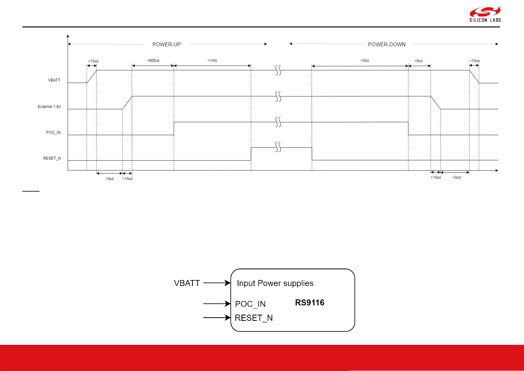
The POC_IN and RESET_N signals should be controlled from external sources such as R/C circuits, and/or other MCU's GPIOs. However POC_OUT can be connected to
POC_IN through an R-C, if the supply voltage is 3.3V. Below waveforms show power sequence (Up & Down) requirements under various application needs. Note that
below waveforms are not to scale.
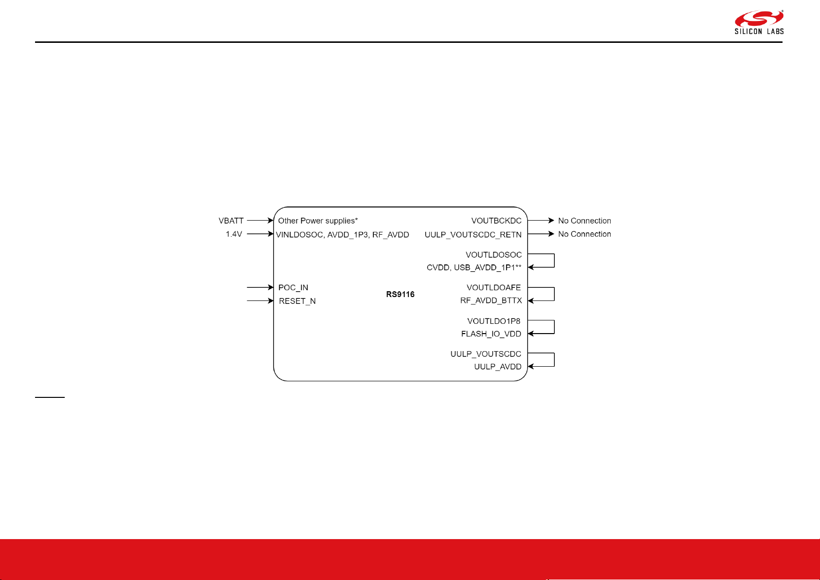
3.3.2.1 Power-Up and Down Sequence with External 1.4V supply and POC_IN
The diagram below shows connections of various power supply voltages, POC_IN and RESET_N. These connections can be used when:
• System PMU (outside RS9116) can provide 1.4V supply, and hence the internal Buck regulator in RS9116 can be disabled.
• The 1.1V supply is still derived from LDO SoC (internal to RS9116).
• POC_IN is controlled externally.
NOTE:
1. Above shown is a typical connection diagram. Some of the supply pins shown above may or may not be present in the IC/Module. Check the Pinout table in this
datasheet and connect accordingly.
2. * = Provide the supply voltages as per the specifications mentioned in this datasheet.
3. ** = USB power supply input connection is required if USB interface is present and used. Else, follow the connection as shown in Reference Schematics.
silabs.com | Building a more connected world. Rev 1.0.8 26 | Page
PRELIMINARY | Subject to change.
Page 28
RS9116 CC1 Connectivity Module Datasheet v1.0.8, Dec-2020
silabs.com | Building a more connected world. Rev 1.0.8 27 | Page
PRELIMINARY | Subject to change.
NOTE:
1. VBATT supply shown above must be connected to the power supply pins of IC/Module. For example, SDIO_IO_VDD, ULP_IO_VDD, UULP_VBATT_1, etc.
2. Above POC_IN waveform is applicable if it is externally driven. Else, that particular waveform can be ignored, and the RESET_N timing can be considered after/before
external power supplies ramp-up/down.
3.3.2.2 Power-Up and Down Sequence with External POC_IN
The diagram below shows connections of various power supply voltages, POC_IN and RESET_N. These connections can be used when:
• System PMU cannot provide 1.4V or 1.1V supplies and the internal buck and LDO of RS9116 are used.
• POC_IN is controlled externally.
Page 29
RS9116 CC1 Connectivity Module Datasheet v1.0.8, Dec-2020
silabs.com | Building a more connected world. Rev 1.0.8 28 | Page
PRELIMINARY | Subject to change.
NOTE:
1. Above shown is a typical connection diagram. Check the Reference Schematics for connections of other power supplies.
NOTE:
1. VBATT supply shown above must be connected to the power supply pins of IC/Module. For example, SDIO_IO_VDD, ULP_IO_VDD, UULP_VBATT_1, etc.
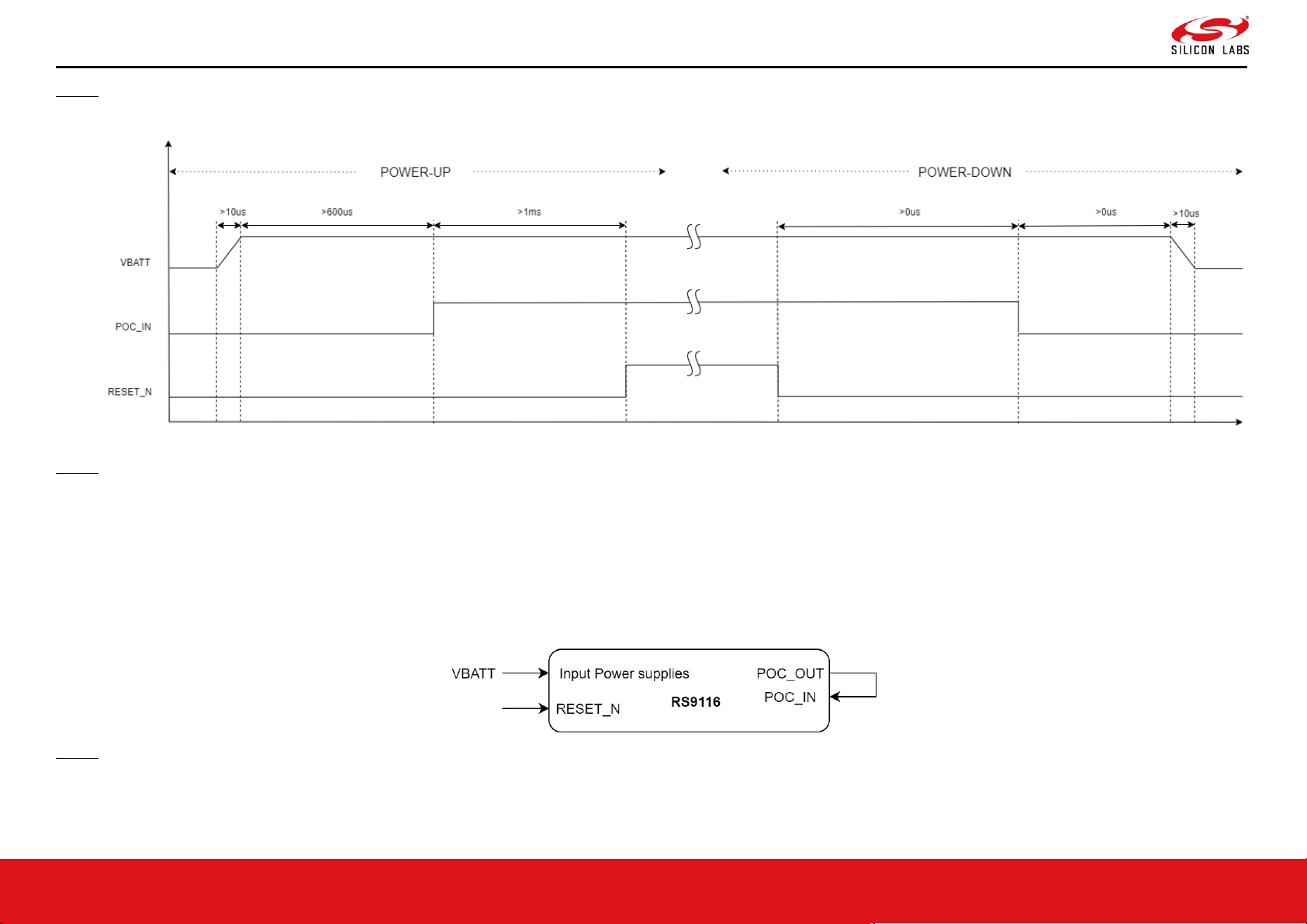
3.3.2.3 Power-Up and Down Sequence with POC_IN Connected Internally
The diagram below shows connections of various power supply voltages, POC_IN and RESET_N. The typical applications of this connection can be as followws.
• System cannot provide external 1.4V & 1.1V supplies and the internal buck and LDO of RS9116 are used.
• POC_IN is looped back from POC_OUT.
NOTE:
1. Above shown is a typical connection diagram. Check the Reference Schematics for connections of other power supplies.
2. POC_OUT can be connected to POC_IN if the supply voltage is 3.3V only. Else, POC_IN has to be driven externally.
Page 30
RS9116 CC1 Connectivity Module Datasheet v1.0.8, Dec-2020
silabs.com | Building a more connected world. Rev 1.0.8 29 | Page
PRELIMINARY | Subject to change.
NOTE:
1. VBATT supply shown above must be connected to the power supply pins of IC/Module. For example, SDIO_IO_VDD, ULP_IO_VDD, UULP_VBATT_1, etc.
Page 31

RS9116 CC1 Connectivity Module Datasheet v1.0.8, Dec-2020
silabs.com | Building a more connected world. Rev 1.0.8 30 | Page
PRELIMINARY | Subject to change.
3.3.3 Digital Input Output Signals
Symbol
Parameter
Min.
Typ.
Max.
Unit
VIH
High level input voltage @3.3V
2.0 - 3.63
V
High level input voltage @1.8V
1.17 - 2.1
V
VIL
Low level input voltage @3.3V
-0.3 - 0.8
V
Low level input voltage @1.8V
-0.3
-
0.63
V
V
hys
Hysteresis voltage
0.1 VDD
-
-
V
VOL
Low level output voltage
- - 0.4
V
VOH
High level output voltage
VDD-0.4
- - V
IOL
Low level output current (programmable)
2.0
4.0
12.0
mA
IOH
High level output current (programmable)
2.0
4.0
12.0
mA
Table 8. Digital I/O Signals
3.3.4 USB
Parameter
Conditions
Min.
Typ.
Max.
Units
Vcm DC (DC level measured at receiver
connector)
HS Mode
LS/FS Mode
-0.05
0.8
-
0.5
2.5
V
Crossover Voltages
LS Mode
FS Mode
1.3
1.3
-
2 2 V
Power supply ripple noise (Analog 3.3V)
< 160 MHz
-50 - 50
mV
Table 9. USB
3.3.5 Pin Capacitances
Symbol
Parameter
Min.
Typ.
Max.
Unit
Cio
Input/output capacitance, digital pins only
- - 2.0
pF
Table 10. Pin Capacitances
3.4 AC Characteristics
3.4.1 Clock Specifications
RS9116 chipsets require two primary clocks:
• Low frequency 32 kHz clock for sleep manager and RTC
o Internal 32 kHz RC clock is used for applications with low timing accuracy requirements
o 32 kHz crystal clock is used for applications with high timing accuracy requirements
• High frequency 40 MHz clock for the ThreadArch® processor, baseband subsystem and the radio
The chipsets have integrated internal oscillators including crystal oscillators to generate the required clocks.
Integrated crystal oscillators enable the use of low-cost passive crystal components. Additionally, in a system where
an external clock source is already present, the clock can be reused. The following are the recommended options for
the clocks for different functionalities:
Page 32

RS9116 CC1 Connectivity Module Datasheet v1.0.8, Dec-2020
silabs.com | Building a more connected world. Rev 1.0.8 31 | Page
PRELIMINARY | Subject to change.
Functionality
Default Clock
option
Other Clock option
Comments
Wi-Fi or Wi-Fi + BLE
Connectivity
Internal 32 kHz RC
oscillator calibrated
to <200ppm
32 kHz XTAL
oscillator input on
UULPGPIO.
32 kHz XTAL Oscillator clock is optional.
No significant power consumption
impact on connected power numbers
(<10uA).
Wi-Fi + BT or Wi-Fi + BT + BLE
Connectivity with low power
Audio Streaming operation
(A2DP Source)
32 kHz XTAL
oscillator input on
UULPGPIO
Internal 32 kHz RC
oscillator calibrated
to <200ppm
32 kHz XTAL Oscillator clock is
important for Low-power Audio
Streaming operation (A2DP Source).
There is no impact on sleep/deep-sleep power consumption with/without 32 kHz XTAL oscillator clock
32 kHz XTAL sources:
Option 1: From Host MCU/MPU LVCMOS rail to rail clock input on UULPGPIO
Option 2: External Xtal oscillator providing LVCMOS rail to rail clock input on UULPGPIO (Nano-drive clock should
not be supplied).
3.4.1.1 32 kHz Clock
The 32 kHz clock selection can be done through software. RC oscillator clock is not suited for high timing accuracy
applications and can increase system current consumption in duty-cycled power modes.
3.4.1.1.1 RC Oscillator
Parameter
Parameter Description
Min
Typ
Max
Units
F
osc
Oscillator Frequency
32.0
kHz
F
osc_Acc
Frequency Variation with Temp and Voltage
1.2 %
Jitter
RMS value of Edge jitter (TIE)
91 ns
Peak Period Jitter
Peak value of Cycle Jitter with 6σ variation
789 ns
Table 11. 32 kHz RC Oscillator
3.4.1.1.2 32 kHz External Oscillator
An external 32 kHz low-frequency clock can be fed through the XTAL_32KHZ_IN functionality.
Figure 6. External 32 kHz Oscillator - Rail to Rail
Page 33

RS9116 CC1 Connectivity Module Datasheet v1.0.8, Dec-2020
silabs.com | Building a more connected world. Rev 1.0.8 32 | Page
PRELIMINARY | Subject to change.
Parameter
Parameter Description
Min
Typ
Max
Units
F
osc
Oscillator Frequency
32.768
kHz
F
osc_Acc
Frequency Variation with Temp and Voltage
-100
100
ppm
Duty cycle
Input duty cycle
30
50
70
%
VAC
Input AC peak-peak voltage swing at input
pin.
0.3
-
VBATT-
0.3
Vpp
Table 12. 32 kHz External Oscillator Specifications
3.4.1.2 40 MHz Clock
Load capacitance with 40 MHz internal oscillator is integrated inside the chipset and calibrated. The calibrated value
can be stored in eFuse using calibration software. The module provides the below characteristics.
Parameter
Parameter Description
Min
Typ
Max
Units
F
osc
Oscillator Frequency
40 MHz
F
osc_Acc
Frequency Variation with Temp and Voltage
-20 20
ppm
ESR
Equivalent series resistance
60
Ω
Load cap
Load capacitance range
5 10
pF
Table 13. 40 MHz Crystal Specifications
3.4.2 SDIO 2.0 Slave
3.4.2.1 Full Speed Mode
Parameter
Parameter Description
Min.
Typ.
Max.
Unit
T
sdio
SDIO_CLK
- - 25
MHz
Ts
SDIO_DATA, input setup time
4 - -
ns
Th
SDIO_DATA, input hold time
1 - -
ns
Tod
SDIO_DATA, clock to output delay
- - 13
ns
CL
Output Load
5 - 10
pF
Table 14. AC Characteristics - SDIO 2.0 Slave Full Speed Mode
Figure 7. Interface Timing Diagram for SDIO 2.0 Slave Full Speed Mode
Page 34

RS9116 CC1 Connectivity Module Datasheet v1.0.8, Dec-2020
silabs.com | Building a more connected world. Rev 1.0.8 33 | Page
PRELIMINARY | Subject to change.
3.4.2.2 High Speed Mode
Parameter
Parameter Description
Min.
Typ.
Max.
Unit
T
sdio
SDIO_CLK
25 - 50
MHz
Ts
SDIO_DATA, input setup time
4 - -
ns
Th
SDIO_DATA, input hold time
1 - -
ns
Tod
SDIO_DATA, clock to output delay
2.5 - 13
ns
CL
Output Load
5 - 10
pF
Table 15. AC Characteristics - SDIO 2.0 Slave High Speed Mode
Figure 8. Interface Timing Diagram for SDIO 2.0 Slave High Speed Mode
3.4.3 SPI Slave
3.4.3.1 Low Speed Mode
Parameter
Parameter Description
Min.
Typ.
Max.
Unit
T
spi
SPI_CLK
0 - 25
MHz
Tcs
SPI_CS to output delay
- - 7.5
ns
T
cst
SPI CS to input setup time
4.5 - -
-
Ts
SPI_MOSI, input setup time
1.33 - -
ns
Th
SPI_MOSI, input hold time
1.2 - -
ns
Tod
SPI_MISO, clock to output delay
- - 8.75
ns
CL
Output Load
5 - 10
pF
Table 16. AC Characteristics - SPI Slave Low Speed Mode
Page 35

RS9116 CC1 Connectivity Module Datasheet v1.0.8, Dec-2020
silabs.com | Building a more connected world. Rev 1.0.8 34 | Page
PRELIMINARY | Subject to change.
Figure 9. Interface Timing Diagram for SPI Slave Low Speed Mode
3.4.3.2 High Speed Mode
Parameter
Parameter Description
Min.
Typ.
Max.
Unit
T
spi
SPI_CLK
25 - 80
MHz
Tcs
SPI_CS to output delay
- - 7.5
ns
T
cst
SPI CS to input setup time
4.5 - -
-
Ts
SPI_MOSI, input setup time
1.33 - -
ns
Th
SPI_MOSI, input hold time
1.2 - -
ns
Tod
SPI_MISO, clock to output delay
2.5 - 8.75
ns
CL
Output Load
5 - 10
pF
Table 17. AC Characteristics - SPI Slave High Speed Mode
Figure 10. Interface Timing Diagram for SPI Slave High Speed Mode
3.4.3.3 Ultra High Speed Mode
Parameter
Parameter Description
Min.
Typ.
Max.
Unit
T
spi
SPI_CLK
- - 100
MHz
Ts
SPI_MOSI, input setup time
1.33 - -
ns
Page 36

RS9116 CC1 Connectivity Module Datasheet v1.0.8, Dec-2020
silabs.com | Building a more connected world. Rev 1.0.8 35 | Page
PRELIMINARY | Subject to change.
Parameter
Parameter Description
Min.
Typ.
Max.
Unit
Th
SPI_MOSI, input hold time
1.2 - -
ns
Tod
SPI_MISO, clock to output delay
1.5 - 8.75
ns
CL
Output Load
5 - 10
pF
Table 18. AC Characteristics - SPI Slave Ultra High Speed Mode
Figure 11. Interface Timing Diagram for SPI Slave Ultra High Speed Mode
3.4.4 USB
3.4.4.1 Low Speed Mode
Parameter
Parameter Description
Min.
Typ.
Max.
Unit
Tr
Rise Time
75 - 300
ns
Tf
Fall Time
75 - 300
ns
Jitter
Jitter - -
10
ns
Table 19. AC Characteristics - USB Low Speed Mode
3.4.4.2 Full Speed Mode
Parameter
Parameter
Min.
Typ.
Max.
Unit
Tr
Rise Time
4 - 20
ns
Tf
Fall Time
4 - 20
ns
Jitter
Jitter - - 1 ns
Table 20. AC Characteristics - USB Full Speed Mode
3.4.4.3 High Speed Mode
Parameter
Parameter Description
Min.
Typ.
Max.
Unit
Tr
Rise Time
0.5 - -
ns
Tf
Fall Time
0.5 - -
ns
Jitter
Jitter - -
0.1
ns
Table 21. AC Characteristics - USB High Speed Mode
Page 37

RS9116 CC1 Connectivity Module Datasheet v1.0.8, Dec-2020
silabs.com | Building a more connected world. Rev 1.0.8 36 | Page
PRELIMINARY | Subject to change.
3.4.5 UART
Parameter
Parameter Description
Min.
Typ.
Max.
Unit
T
uart
CLK 0 -
20
MHz
Tod
Output delay
0 - 10
ns
Ts
Input setup time
0 - 5
ns
CL
Output load
5 - 25
pF
Table 22. AC Characteristics - UART
3.4.6 I2C Master and Slave
3.4.6.1 Fast Speed Mode
Parameter
Parameter Description
Min.
Typ.
Max.
Unit
T
i2c
SCL
100 - 400
KHz
T
low
clock low period
1.3 - -
us
T
high
clock high period
0.6 - -
us
T
sstart
start condition, setup time
0.6 - -
us
T
hstart
start condition, hold time
0.6 - -
us
Ts
data, setup time
100 - -
ns
T
sstop
stop condition, setup time
0.6 - -
us
CL
Output Load
5 - 10
pF
Table 23. AC Characteristics - I2C Fast Speed Mode
Figure 12. Interface Timing Diagram for I2C Fast Speed Mode
3.4.6.2 High Speed Mode
Parameter
Parameter Description
Min.
Typ.
Max.
Unit
T
i2c
SCL
0.4 - 3.4
MHz
T
low
clock low period
160 - -
ns
T
high
clock high period
60 - -
ns
T
sstart
start condition, setup time
160 - -
ns
T
hstart
start condition, hold time
160 - -
ns
Ts
data, setup time
10 - -
ns
Page 38

RS9116 CC1 Connectivity Module Datasheet v1.0.8, Dec-2020
silabs.com | Building a more connected world. Rev 1.0.8 37 | Page
PRELIMINARY | Subject to change.
Parameter
Parameter Description
Min.
Typ.
Max.
Unit
Th
data, hold time
0 - 70
ns
T
sstop
stop condition, setup time
160 - -
ns
CL
Output Load
5 - 10
pF
Table 24. AC Characteristics - I2C High Speed Mode
Figure 13. Interface Timing Diagram for I2C High Speed Mode
3.4.7 I2S/PCM Master and Slave
3.4.7.1 Master Mode
Negedge driving and posedge sampling for I2S
Posedge driving and negedge sampling for PCM
Parameter
Parameter Description
Min.
Typ.
Max.
Unit
T
i2s
i2s_clk 0 -
25
MHz
Ts
i2s_din,i2s_ws setup time
10 - -
ns
Th
i2s_din,i2s_ws hold time
0 - -
ns
Tod
i2s_dout output delay
0 - 12
ns
CL
i2s_dout output load
5 - 10
pF
Table 25. AC Characteristics – I2S/PCM Master Mode
Figure 14. Interface Timing Diagram for I2S Master Mode
Page 39

RS9116 CC1 Connectivity Module Datasheet v1.0.8, Dec-2020
silabs.com | Building a more connected world. Rev 1.0.8 38 | Page
PRELIMINARY | Subject to change.
3.4.7.2 Slave Mode
Negedge driving and posedge sampling for I2S
Posedge driving and negedge sampling for PCM
Parameter
Parameter Description
Min.
Typ.
Max.
Unit
T
i2s
i2s_clk 0 -
25
MHz
Ts
i2s_din,i2s_ws setup time
8 - -
ns
Th
i2s_din,i2s_ws hold time
0 - -
ns
Tod
i2s_dout output delay
0 - 17
ns
CL
i2s_dout output load
5 - 10
pF
Table 26. AC Characteristics - I2S/PCM Slave Mode
Figure 15. Interface Timing Diagram for I2S Slave Mode
3.4.8 GPIO pins
Parameter
Parameter
Description
Conditions
Min.
Typ.
Max.
Unit
Trf
Rise time
Pin configured as output; SLEW =
1(fast mode)
1.0 - 2.5
ns
Tff
Fall time
Pin configured as output; SLEW =
1(fast mode)
0.9 - 2.5
ns
Trs
Rise time
Pin configured as output; SLEW =
0(standard mode)
1.9 - 4.3
ns
Tfs
Fall time
Pin configured as output; SLEW =
0(standard mode)
1.9 - 4.0
ns
Tr
Rise time
Pin configured as input
0.3 - 1.3
ns
Tf
Fall time
Pin configured as input
0.2 - 1.2
ns
Table 27. AC Characteristics - GPIO Pins
Page 40

RS9116 CC1 Connectivity Module Datasheet v1.0.8, Dec-2020
In the sub-sections below,
Unless otherwise stated, the specifications in this section apply when the operating conditions are within the
limits specified in the Recommended Operating Conditions
TA = 25°C, PA2G_AVDD/VINBCKDC = 3.3V. Remaining supplies are at typical operating conditions.
Parameters are measured at antenna port on channel 6 (2437 MHz)
(1)
Parameter
Condition
Notes
Min
Typ
Max
Units
Transmit Power for 20 MHz
Bandwidth, compliant with IEEE
mask and EVM
DSSS - 1 Mbps
EVM< -9 dB
-
17.5
-
dBm
DSSS - 2 Mbps
EVM< -9 dB
-
17.5
-
dBm
CCK- 5.5 Mbps
EVM< -9 dB
-
17.5
-
dBm
CCK - 11 Mbps
EVM< -9 dB
-
17.5
-
dBm
OFDM - 6 Mbps
EVM< -5 dB
-
15.5
-
dBm
OFDM - 9 Mbps
EVM< -8 dB
-
15.5
-
dBm
OFDM - 12
Mbps
EVM< -10 dB
-
15.5
-
dBm
OFDM - 18
Mbps
EVM< -13 dB
-
16 - dBm
OFDM - 24
Mbps
EVM< -16 dB
-
15.5
-
dBm
OFDM - 36
Mbps
EVM< -19 dB
-
13.5
-
dBm
OFDM - 48
Mbps
EVM< -22 dB
-
13 - dBm
OFDM - 54
Mbps
EVM< -25 dB
-
13 - dBm
MCS0 Mixed
Mode
EVM< -5 dB
-
16 - dBm
MCS1 Mixed
Mode
EVM< -10 dB
-
16 - dBm
MCS2 Mixed
Mode
EVM< -13 dB
-
16 - dBm
3.5 RF Characteristics
• All WLAN Sensitivity numbers and Adjacent channel numbers are at < 10% PER limit for 802.11 a/g/n OFDM
data rates, and < 8% PER limit for 802.11 b DSSS/CCA data rates. Packet sizes are 1024 bytes for 802.11 b/
g data rates and 4096 bytes for 802.11n data rates.
• For WLAN ACI cases, the desired signal power is 3dB above standard defined sensitivity level.
• For Bluetooth C/I cases, the desired signal power is 3dB above standard defined sensitivity level.
3.5.1 WLAN 2.4 GHz Transmitter Characteristics
3.5.1.1 Transmitter Characteristics with 3.3V Supply
silabs.com | Building a more connected world. Rev 1.0.8 39 | Page
PRELIMINARY | Subject to change.
Page 41

RS9116 CC1 Connectivity Module Datasheet v1.0.8, Dec-2020
silabs.com | Building a more connected world. Rev 1.0.8 40 | Page
PRELIMINARY | Subject to change.
Parameter
Condition
Notes
Min
Typ
Max
Units
MCS3 Mixed
Mode
EVM< -16 dB
-
15.5
-
dBm
MCS4 Mixed
Mode
EVM< -19 dB
-
13.5
-
dBm
MCS5 Mixed
Mode
EVM< -22 dB
-
12.5
-
dBm
MCS6 Mixed
Mode
EVM< -25 dB
-
12.5
-
dBm
MCS7 Mixed
Mode
EVM< -27 dB
-
11 - dBm
Transmitter Emissions (6 Mbps @
Maximum Power)
776-794 MHz
CDMA2000
-
-148
-
dBm/Hz
869–960 MHz
CDMAOne,
GSM850
-
-158
-
dBm/Hz
1450–1495 MHz
DAB - -151
-
dBm/Hz
1570–1580 MHz
GPS - -151
-
dBm/Hz
1592–1610 MHz
GLONASS
-
-132
-
dBm/Hz
1710–1800 MHz
DSC-1800Uplink
-
-130
-
dBm/Hz
1805–1880 MHz
GSM 1800
-
-110
-
dBm/Hz
1850–1910 MHz
GSM 1900
-
-122
-
dBm/Hz
1910–1930 MHz
TDSCDMA,LTE
-
-135
-
dBm/Hz
1930–1990 MHz
GSM1900,
CDMAOne,WCD
MA
-
-130
-
dBm/Hz
2010–2075 MHz
TDSCDMA
-
-127
-
dBm/Hz
2110–2170 MHz
WCDMA
-
-119
-
dBm/Hz
2305–2370 MHz
LTE Band 40
-
-112
-
dBm/Hz
2370–2400 MHz
LTE Band 40
-
-95
-
dBm/Hz
2496–2530 MHz
LTE Band 41
-
-102
-
dBm/Hz
2530–2560 MHz
LTE Band 41
-
-113
-
dBm/Hz
2570–2690 MHz
LTE Band 41
-
-128
-
dBm/Hz
5000–5900 MHz
WLAN 5G
-
-148
-
dBm/Hz
Harmonic Emissions (1 Mbps @
Maximum Power)
4.8-5.0 GHz
2nd Harmonic
-
-40
-
dBm/MHz
7.2-7.5 GHz
3rd Harmonic
-
-43
-
dBm/MHz
Table 28. WLAN 2.4 GHz Transmitter Characteristics (3.3V)
1. Up to 2dB variation in power from channel-to-channel. To meet FCC emission limits, edge channels (1 and
11) have reduced TX power.
Page 42

RS9116 CC1 Connectivity Module Datasheet v1.0.8, Dec-2020
silabs.com | Building a more connected world. Rev 1.0.8 41 | Page
PRELIMINARY | Subject to change.
3.5.2 WLAN 2.4 GHz Receiver Characteristics on High-Performance (HP) RF Chain
TA = 25°C. Parameters are measured at antenna port on channel 1(2412 MHz)
Parameter
Condition/Notes
Min
Typ
Max
Units
Sensitivity for 20 MHz
Bandwidth
(1)
1 Mbps DSSS
-
-96
-
dBm
2 Mbps DSSS
-
-90
-
dBm
5.5 Mbps CCK
-
-89
-
dBm
11 Mbps CCK
-
-86.5
-
dBm
6 Mbps OFDM
-
-90
-
dBm
9 Mbps OFDM
-
-89
-
dBm
12 Mbps OFDM
-
-89
-
dBm
18 Mbps OFDM
-
-87
-
dBm
24 Mbps OFDM
-
-84
-
dBm
36 Mbps OFDM
-
-80
-
dBm
48 Mbps OFDM
-
-75.5
-
dBm
54 Mbps OFDM
-
-74
-
dBm
MCS0 Mixed Mode
-
-89.5
-
dBm
MCS1 Mixed Mode
-
-87
-
dBm
MCS2 Mixed Mode
-
-84
-
dBm
MCS3 Mixed Mode
-
-82
-
dBm
MCS4 Mixed Mode
-
-78
-
dBm
MCS5 Mixed Mode
-
-73
-
dBm
MCS6 Mixed Mode
-
-71
-
dBm
MCS7 Mixed Mode
-
-70
-
dBm
Maximum Input Level for PER
below 10%
802.11 b
- 8 -
dBm
802.11g
-
-10
-
dBm
802.11n
-
-10
-
dBm
RSSI Accuracy Range
-3 - 3
dB
Blocking level for 3 dB RX
Sensitivity Degradation(Data rate
6Mbps OFDM, Desired signal at 79dBm)
776–794 MHz
-
-6 - dBm
824–849 MHz
-
-5 - dBm
880–915 MHz
-
-8 - dBm
1710–1785 MHz
-
-21
-
dBm
1850–1910 MHz
-
-17
-
dBm
1920–1980 MHz
-
-20
-
dBm
2300–2400 MHz
-
-58
-
dBm
Page 43

RS9116 CC1 Connectivity Module Datasheet v1.0.8, Dec-2020
silabs.com | Building a more connected world. Rev 1.0.8 42 | Page
PRELIMINARY | Subject to change.
Parameter
Condition/Notes
Min
Typ
Max
Units
2570–2620 MHz
-
-22
-
dBm
2545–2575 MHz
-
-20
-
dBm
Return Loss
-10 - -
dB
Adjacent Channel Interference
1 Mbps DSSS
-
36 - dB
11 Mbps DSSS
-
37 - dB
6 Mbps OFDM
-
38 - dB
54 Mbps OFDM
-
22 - dB
MCS0 Mixed Mode
-
38 - dB
MCS7 Mixed Mode
-
20 - dB
Alternate Adjacent Channel
Interference
1 Mbps DSSS
-
44 - dB
11 Mbps DSSS
-
35 - dB
6 Mbps OFDM
-
46 - dB
54 Mbps OFDM
-
30 - dB
MCS0 Mixed Mode
-
46 - dB
MCS7 Mixed Mode
-
28 - dB
Table 29. WLAN 2.4 GHz Receiver Characteristics on HP RF Chain
1. Sensitivities for channels 6,7,8 & 11 are up to 2dB worse
3.5.3 WLAN 2.4 GHz Receiver Characteristics on Low-Power (LP) RF Chain
TA = 25°C. Parameters are measured at antenna port on channel 1(2412 MHz)
Parameter
Condition
Min
Typ
Max
Units
Sensitivity for 20 MHz
Bandwidth
(1)
1 Mbps DSSS
-
-94
-
dBm
2 Mbps DSSS
-
-87.5
-
dBm
5.5 Mbps CCK
-
-86.5
-
dBm
11 Mbps CCK
-
-83.5
-
dBm
6 Mbps OFDM
-
-87.5
-
dBm
9 Mbps OFDM
-
-87
-
dBm
12 Mbps OFDM
-
-86.5
-
dBm
18 Mbps OFDM
-
-84
-
dBm
24 Mbps OFDM
-
-81
-
dBm
36 Mbps OFDM
-
-77
-
dBm
MCS0 Mixed Mode
-
-87
-
dBm
Page 44

RS9116 CC1 Connectivity Module Datasheet v1.0.8, Dec-2020
silabs.com | Building a more connected world. Rev 1.0.8 43 | Page
PRELIMINARY | Subject to change.
Parameter
Condition
Min
Typ
Max
Units
MCS1 Mixed Mode
-
-84.5
-
dBm
MCS2 Mixed Mode
-
-82
-
dBm
MCS3 Mixed Mode
-
-79
-
dBm
MCS4 Mixed Mode
-
-75
-
dBm
Maximum Input Level for PER
below 10%
802.11 b
- 0 -
dBm
802.11g
-
-10
-
dBm
802.11n
-
-10
-
dBm
RSSI Accuracy Range
-3
- 3
dB
Blocking level for 3 dB RX
Sensitivity Degradation(Data rate
6Mbps OFDM, Desired signal at 79dBm)
776–794 MHz
-
-8 - dBm
824–849 MHz
-
-8 - dBm
880–915 MHz
-
-10
-
dBm
1710–1785 MHz
-
-16
-
dBm
1850–1910 MHz
-
-14
-
dBm
1920–1980 MHz
-
-20
-
dBm
2300–2400 MHz
-
-55
-
dBm
2570–2620 MHz
-
-24
-
dBm
2545–2575 MHz
-
-23
-
dBm
Return Loss
-10 - -
dB
Adjacent Channel Interference
1 Mbps DSSS
-
40 - dB
11 Mbps DSSS
-
36 - dB
6 Mbps OFDM
-
42 - dB
36 Mbps OFDM
-
30 - dB
MCS0 Mixed Mode
-
40 - dB
MCS4 Mixed Mode
-
30 - dB
Alternate Adjacent Channel
Interference
1 Mbps DSSS
-
50 - dB
11 Mbps DSSS
-
38 - dB
6 Mbps OFDM
-
48 - dB
36 Mbps OFDM
-
38 - dB
MCS0 Mixed Mode
-
48 - dB
MCS4 Mixed Mode
-
36 - dB
Table 30. WLAN 2.4 GHz Receiver Characteristics on LP RF Chain
1. Sensitivities for channels 6,7,8 & 11 are up to 2dB worse.
Page 45

RS9116 CC1 Connectivity Module Datasheet v1.0.8, Dec-2020
silabs.com | Building a more connected world. Rev 1.0.8 44 | Page
PRELIMINARY | Subject to change.
3.5.4 Bluetooth Transmitter Characteristics on High-Performance (HP) RF Chain
3.5.4.1 Transmitter Characteristics with 3.3 V Supply
TA = 25°C, PA2G_AVDD/VINBCKDC = 3.3 V. Remaining supplies are at typical operating conditions.
Parameters are measured at the antenna port.
(1)
Parameter
Condition
Notes
Min
Typ
Max
Units
Transmit Power
BR -
12 - dBm
EDR 2Mbps
- 12 - dBm
EDR 3Mbps
- 11 - dBm
LE 1Mbps
- 17 - dBm
LE 2Mbps
- 17 - dBm
LR 500 Kbps
- 17 - dBm
LR 125 Kbps
- 17 - dBm
Power Control Step
BR, EDR
- 3 - dB
Adjacent Channel Power |M-N| = 2
BR - - -20
dBm
EDR - - -20
dBm
LE - - -20
dBm
LR - - -20
dBm
Adjacent Channel Power |M-N| > 2
BR - - -40
dBm
EDR - - -40
dBm
LE - - -30
dBm
LR - - -30
dBm
BR Modulation Characteristics
DH1 -25 - 25
kHz
DH3 -40 - 40
kHz
DH5 -40 - 40
kHz
Drift Rate
-20 - 20
kHz/50 us
Δf1 Avg
140 - 175
kHz
Δf2 Max
115 -
kHz
EDR Modulation Characteristics
RMS DEVM,
EDR2
-
15
-
%
RMS DEVM,
EDR3
-
5.5
-
%
99% DEVM,
EDR2
-
23
-
%
99% DEVM,
EDR3
-
9.5
-
%
peak DEVM,
EDR2
-
28
-
%
Page 46

RS9116 CC1 Connectivity Module Datasheet v1.0.8, Dec-2020
silabs.com | Building a more connected world. Rev 1.0.8 45 | Page
PRELIMINARY | Subject to change.
Parameter
Condition
Notes
Min
Typ
Max
Units
peak DEVM,
EDR3
-
13.5
-
%
BLE Modulation Characteristics
Δf1 Avg
225 - 275
kHz
Δf2 Max
185 - -
kHz
Δf2 Avg/Δf1 Avg
0.8 - -
-
Transmitter Emissions (BR
@Maximum output power)
776-794 MHz
CDMA2000
-
-160
-
dBm/Hz
869–960 MHz
CDMAOne,
GSM850
-
-160
-
dBm/Hz
1450–1495 MHz
DAB - -160
-
dBm/Hz
1570–1580 MHz
GPS
-
-160
-
dBm/Hz
1592–1610 MHz
GLONASS
-
-160
(2)
-
dBm/Hz
1710–1800 MHz
DSC-1800Uplink
-
-115
-
dBm/Hz
1805–1880 MHz
GSM 1800
-
-148
-
dBm/Hz
1850–1910 MHz
GSM 1900
-
-148
-
dBm/Hz
1910–1930 MHz
TDSCDMA,LTE
-
-135
-
dBm/Hz
1930–1990 MHz
GSM1900,
CDMAOne,
WCDMA
-
-101
-
dBm/Hz
2010–2075 MHz
TDSCDMA
-
-148
-
dBm/Hz
2110–2170 MHz
WCDMA
-
-115
-
dBm/Hz
2305–2370 MHz
LTE Band 40
-
-140
-
dBm/Hz
2370–2400 MHz
LTE Band 40
-
-134
-
dBm/Hz
2496–2530 MHz
LTE Band 41
-
-125
-
dBm/Hz
2530–2560 MHz
LTE Band 41
-
-138
-
dBm/Hz
2570–2690 MHz
LTE Band 41
-
-138
-
dBm/Hz
5000–5900 MHz
WLAN 5G
-
-148
-
dBm/Hz
Table 31. Bluetooth Transmitter Characteristics on HP RF Chain 3.3V
1. Up to 2dB variation in power from channel-to-channel.
2. Noise-floor is -160dBm/Hz with spurious tone power of -68dBm at 1601.33 MHz when the transmitted signal
is at 2402 MHz
3.5.5 Bluetooth Transmitter Characteristics on Low-Power (LP) 0 dBm RF Chain
TA = 25°C. Parameters are measured at the antenna port and applicable to PA2G_AVDD/VINBCKDC=3.3V
Page 47

RS9116 CC1 Connectivity Module Datasheet v1.0.8, Dec-2020
silabs.com | Building a more connected world. Rev 1.0.8 46 | Page
PRELIMINARY | Subject to change.
Parameter
Condition/Notes
Min
Typ
Max
Units
Transmit Power
BR - -
-3.5
dBm
LE 1Mbps
- - -3.5
dBm
LE 2Mbps
- - -3.5
dBm
LR 500 Kbps
- - -3.5
dBm
LR 125 kbps
- - -3.5
dBm
Adjacent Channel Power |M-N| = 2
BR - -
-20
dBm
LE - -
-20
dBm
LR - -
-20
dBm
Adjacent Channel Power |M-N| > 2
BR - -
-40
dBm
LE - -
-30
dBm
LR - -
-30
dBm
BR Modulation Characteristics
DH1
-25 - 25
kHz
DH3
-40 - 40
kHz
DH5
-40 - 40
kHz
Drift Rate
-20 - 20
kHz
Δf1 Avg
140 - 175
kHz
Δf2 Max
115 - -
kHz
BLE Modulation Characteristics
Δf1 Avg
225 - 275
kHz
Δf2 Max
185 - -
kHz
Δf2 Avg/Δf1 Avg
0.8
1.5 - -
Table 32. Bluetooth Transmitter Characteristics on LP 0 dBm RF Chain
3.5.6 Bluetooth Receiver Characteristics on High-Performance (HP) RF Chain
TA = 25°C. Parameters are measured at the antenna port and applicable to PA2G_AVDD/VINBCKDC=3.3V
Parameter
Condition/Notes
Min
Typ
Max
Units
Sensitivity,Dirty TX off
(1),(2)
BR (1 Mbps), 339 bytes, DH5
Packet, BER= 0.1%
-
-90.5
-
dBm
EDR2 (2 Mbps), 679 bytes, 2-DH5
Packet, BER= 0.01%
-
-91.5
-
dBm
EDR3 (3 Mbps), 1020 bytes, 3DH5 Packet, BER= 0.01%
-
-84.5
-
dBm
LE (1 Mbps), 37 bytes,
PER=30.8%
-
-92
-
dBm
LE (2 Mbps), 37 bytes,
PER=30.8%
-
-90
-
dBm
Page 48

RS9116 CC1 Connectivity Module Datasheet v1.0.8, Dec-2020
silabs.com | Building a more connected world. Rev 1.0.8 47 | Page
PRELIMINARY | Subject to change.
Parameter
Condition/Notes
Min
Typ
Max
Units
LR (500 Kbps), 37 bytes,
PER=30.8%
-
-99
-
dBm
LR (125 Kbps), 37 bytes,
PER=30.8%
-
-103
-
dBm
Maximum Input Level
BR, EDR2, EDR3,BER= 0.1%
-
-15
-
dBm
LE 1Mbps, 2Mbps,PER=30.8%
-
-1 - dBm
LR 500kps, 125kbps,PER=30.8%
-
>10
-
dBm
C/I Performance
BR, co-channel, BER=0.1%
9 - -
dB
BR, adjacent +1/-1 MHz,
BER=0.1%
-2 - -
dB
BR, adjacent +2/-2 MHz
BER=0.1%
-19 - -
dB
BR, adjacent >=|±3| MHz
BER=0.1%
-19 - -
dB
BR, Image channel BER=0.1%
-11 - -
dB
BR, adjacent to Image channel
BER=0.1%
-22 - -
dB
EDR2, co-channel BER=0.1%
11 - -
dB
EDR2, adjacent +1/-1 MHz
BER=0.1%
-2 - -
dB
EDR2, adjacent +2/-2 MHz
BER=0.1%
-17 - -
dB
EDR2, adjacent >=|±3| MHz
BER=0.1%
-17 - -
dB
EDR2, Image channel BER=0.1%
-9 - -
dB
EDR2, adjacent to Image channel
BER=0.1%
-22 - -
dB
EDR3, co-channel BER=0.1%
19 - -
dB
EDR3, adjacent +1/- MHz
BER=0.1%
3 - -
dB
EDR3, adjacent +2/-2 MHz
BER=0.1%
-12 - -
dB
EDR3, adjacent >=|±3| MHz
BER=0.1%
-12 - -
dB
EDR3, Image channel BER=0.1%
-2 - -
dB
EDR3, adjacent to Image channel
BER=0.1%
-15 - -
dB
LE 1Mbps, co-channel
PER=30.8%
-
10 - dB
LE 1Mbps, adjacent +1 MHz
PER=30.8%
- 1 -
dB
Page 49

RS9116 CC1 Connectivity Module Datasheet v1.0.8, Dec-2020
silabs.com | Building a more connected world. Rev 1.0.8 48 | Page
PRELIMINARY | Subject to change.
Parameter
Condition/Notes
Min
Typ
Max
Units
LE 1Mbps, adjacent -1 MHz
PER=30.8%
-
-2 - dB
LE 1Mbps, adjacent +2 MHz
PER=30.8%
-
-23 - dB
LE 1Mbps, adjacent -2 MHz
PER=30.8%
-
-24 - dB
LE 1Mbps, adjacent +3 MHz
PER=30.8%
-
-21 - dB
LE 1Mbps, adjacent -3 MHz
PER=30.8%
-
-27 - dB
LE 1Mbps, adjacent >= |±4| MHz
PER=30.8%
-
-35 - dB
LE 1Mbps, Image channel
PER=30.8%
-
-24 - dB
LE 1Mbps, +1MHz adjacent to
Image channel PER=30.8%
-
-34 - dB
LE 1Mbps, -1MHz adjacent to
Image channel PER=30.8%
-
-21 - dB
LE 2Mbps, co-channel
PER=30.8%
-
11 - dB
LE 2Mbps, adjacent +2 MHz
PER=30.8%
-
-4 - dB
LE 2Mbps, adjacent -2 MHz
PER=30.8%
-
-4 dB
LE 2Mbps, adjacent +4 MHz
PER=30.8%
-
-13 - dB
LE 2Mbps, adjacent -4 MHz
PER=30.8%
-
-17 dB
LE 2Mbps, adjacent >= |±6| MHz
PER=30.8%
-
-32 - dB
LE 2Mbps, Image channel
PER=30.8%
-
-13 - dB
LE 2Mbps, +2MHz adjacent to
Image channel PER=30.8%
-
-24 - dB
LE 2Mbps, -2MHz adjacent to
Image channel PER=30.8%
-
-4 - dB
Table 33. Bluetooth Receiver Characteristics on HP RF Chain
1. BR, EDR: Sensitivities for channels 38,78 are up to 4dB worse, due to the desensitization of the receiver
from harmonics of the system clock (40MHz)
2. BLE, LR: Sensitivities for channels 19,39 are up to 3dB worse, due to the desensitization of the receiver
from harmonics of the system clock (40MHz)
Page 50

RS9116 CC1 Connectivity Module Datasheet v1.0.8, Dec-2020
silabs.com | Building a more connected world. Rev 1.0.8 49 | Page
PRELIMINARY | Subject to change.
3.5.7 Bluetooth Receiver Characteristics on Low-Power (LP) RF Chain
TA = 25°C. Parameters are measured at the antenna port and applicable to PA2G_AVDD/VINBCKDC=3.3V
Parameter
Condition/Notes
Min
Typ
Max
Units
Sensitivity,Dirty TX off
(1),(2)
BR (1 Mbps), 339 bytes, DH5
Packet BER= 0.1%
-
-86
-
dBm
EDR2 (2 Mbps), 679 bytes, 2-DH5
Packet, BER= 0.01%
-
-87
-
dBm
LE (1 Mbps), 37 bytes,
PER=30.8%
-
-89
-
dBm
LE (2 Mbps), 37
bytes, PER=30.8%
-
-87
-
dBm
LR (500 Kbps), 37 bytes,
PER=30.8%
-
-96.5
-
dBm
LR (125 Kbps), 37
bytes, PER=30.8%
-
-101
-
dBm
Maximum Input Level
BR, EDR2 BER= 0.1%
-
-16
-
dBm
LE 1Mbps, 2Mbps PER=30.8%
- 1 -
dBm
LR 500kps, 125kbps PER=30.8%
-
>10
-
dBm
BER Floor
- 1e-4 - %
C/I Performance
BR, co-channel BER= 0.1%
9 - -
dB
BR, adjacent +1/-1 MHz,
BER=0.1%
-2 - -
dB
BR, adjacent +2/-2 MHz
BER=0.1%
-19 - -
dB
BR, adjacent >=|±3| MHz
BER=0.1%
-19 - -
dB
BR, Image channel BER=0.1%
-11 - -
dB
BR, adjacent to Image channel
BER=0.1%
-22 - -
dB
EDR2, co-channel BER=0.1%
11 - -
dB
EDR2, adjacent +1/-1 MHz
BER=0.1%
-2 - -
dB
EDR2, adjacent +2/-2 MHz
BER=0.1%
-17 - -
dB
EDR2, adjacent >=|±3| MHz
BER=0.1%
-17 - -
dB
EDR2, Image channel BER=0.1%
-9 - -
dB
EDR2, adjacent to Image channel
BER=0.1%
-22 - -
dB
LE 1Mbps, co-channel
PER=30.8%
-
10 - dB
Page 51

RS9116 CC1 Connectivity Module Datasheet v1.0.8, Dec-2020
silabs.com | Building a more connected world. Rev 1.0.8 50 | Page
PRELIMINARY | Subject to change.
Parameter
Condition/Notes
Min
Typ
Max
Units
LE 1Mbps, adjacent +1 MHz
PER=30.8%
- 1 -
dB
LE 1Mbps, adjacent -1 MHz
PER=30.8%
-
-1 - dB
LE 1Mbps, adjacent +2 MHz
PER=30.8%
-
-23 - dB
LE 1Mbps, adjacent -2 MHz
PER=30.8%
-
-23 - dB
LE 1Mbps, adjacent +3 MHz
PER=30.8%
-
-22 - dB
LE 1Mbps, adjacent -3 MHz
PER=30.8%
-
-27 - dB
LE 1Mbps, adjacent >= |±4| MHz
PER=30.8%
-
-33 - dB
LE 1Mbps, Image channel
PER=30.8%
-
-27 - dB
LE 1Mbps, +1MHz adjacent to
Image channel PER=30.8%
-
-35 - dB
LE 1Mbps, -1MHz adjacent to
Image channel PER=30.8%
-
-22 - dB
LE 2Mbps, co-channel
PER=30.8%
-
10 - dB
LE 2Mbps, adjacent +2 MHz
PER=30.8%
-
-5 - dB
LE 2Mbps, adjacent -2 MHz
PER=30.8%
-
-3 - dB
LE 2Mbps, adjacent +4 MHz
PER=30.8%
-
-12 - dB
LE 2Mbps, adjacent -4 MHz
PER=30.8%
-
-18 - dB
LE 2Mbps, adjacent >= |±6| MHz
PER=30.8%
-
-35 - dB
LE 2Mbps, Image channel
PER=30.8%
-
-12 - dB
LE 2Mbps, +2MHz adjacent to
Image channel PER=30.8%
-
-24 - dB
LE 2Mbps, -2MHz adjacent to
Image channel PER=30.8%
-
-5 - dB
Table 34. Bluetooth Receiver Characteristics on LP RF Chain
1. BR, EDR: Sensitivities for channels 38,78 are up to 4dB worse, due to the desensitization of the receiver
from harmonics of the system clock (40MHz)
2. BLE, LR: Sensitivities for channels 19,39 are up to 3dB worse, due to the desensitization of the receiver
from harmonics of the system clock (40MHz)
Page 52

RS9116 CC1 Connectivity Module Datasheet v1.0.8, Dec-2020
silabs.com | Building a more connected world. Rev 1.0.8 51 | Page
PRELIMINARY | Subject to change.
3.5.8 WLAN 5GHz Transmitter Characteristics
TA = 25 °C, Parameters are measured at antenna port on 3 channels and 3 frequency bands
(1)
Parameter
Condition
Notes
Min
Typ
Max
Units
Transmit Power for 20 MHz
Bandwidth, compliant with IEEE
mask and EVM
Frequency Band: 5180 - 5300
MHz
OFDM - 6 Mbps
EVM< -5 dB
-
11 - dBm
OFDM - 9 Mbps
EVM< -8 dB
-
10.5
-
dBm
OFDM - 12
Mbps
EVM< -10 dB
-
11 - dBm
OFDM - 18
Mbps
EVM< -13 dB
-
11 - dBm
OFDM - 24
Mbps
EVM< -16 dB
-
11 - dBm
OFDM - 36
Mbps
EVM< -19 dB
-
10 - dBm
OFDM - 48
Mbps
EVM< -22 dB
-
8.5 - dBm
OFDM - 54
Mbps
EVM< -25 dB
-
7.5 - dBm
MCS0 Mixed
Mode
EVM< -5 dB
-
11 - dBm
MCS1 Mixed
Mode
EVM< -10 dB
-
11.5
-
dBm
MCS2 Mixed
Mode
EVM< -13 dB
-
11.5
-
dBm
MCS3 Mixed
Mode
EVM< -16 dB
-
10.5
-
dBm
MCS4 Mixed
Mode
EVM< -19 dB
-
9.5 - dBm
HT - MCS5
EVM< -22 dB
- 8 -
dBm
HT - MCS6
EVM< -25 dB
- 7 -
dBm
HT - MCS7
EVM< -27 dB
- 5 -
dBm
Transmit Power for 20 MHz
Bandwidth, compliant with IEEE
mask and EVM
Frequency Band: 5500 - 5600
MHz
OFDM - 6 Mbps
EVM< -5 dB
-
11 - dBm
OFDM - 9 Mbps
EVM< -8 dB
-
11.5
-
dBm
OFDM - 12
Mbps
EVM< -10 dB
-
11.5
-
dBm
OFDM - 18
Mbps
EVM< -13 dB
-
11.5
-
dBm
OFDM - 24
Mbps
EVM< -16 dB
-
11.5
-
dBm
OFDM - 36
Mbps
EVM< -19 dB
-
8.5 - dBm
Page 53

RS9116 CC1 Connectivity Module Datasheet v1.0.8, Dec-2020
silabs.com | Building a more connected world. Rev 1.0.8 52 | Page
PRELIMINARY | Subject to change.
Parameter
Condition
Notes
Min
Typ
Max
Units
OFDM - 48
Mbps
EVM< -22 dB
- 7 -
dBm
OFDM - 54
Mbps
EVM< -25 dB
-
6.5 - dBm
MCS0 Mixed
Mode
EVM< -5 dB
-
11.5
-
dBm
MCS1 Mixed
Mode
EVM< -10 dB
-
11.5
-
dBm
MCS2 Mixed
Mode
EVM< -13 dB
-
11.5
-
dBm
MCS3 Mixed
Mode
EVM< -16 dB
-
10.5
-
dBm
MCS4 Mixed
Mode
EVM< -19 dB
-
8.5 - dBm
HT - MCS5
EVM< -22 dB
- 7 -
dBm
HT - MCS6
EVM< -25 dB
- 5 -
dBm
HT - MCS7
EVM< -27 dB
- 4 -
dBm
Transmit Power for 20 MHz
Bandwidth, compliant with IEEE
mask and EVM
Frequency Band: 5725 - 5825
MHz
OFDM - 6 Mbps
EVM< -5 dB
- 9 -
dBm
OFDM - 9 Mbps
EVM< -8 dB
- 9 -
dBm
OFDM - 12
Mbps
EVM< -10 dB
- 9 -
dBm
OFDM - 18
Mbps
EVM< -13 dB
- 9 -
dBm
OFDM - 24
Mbps
EVM< -16 dB
-
9.5 - dBm
OFDM - 36
Mbps
EVM< -19 dB
-
6.5 - dBm
OFDM - 48
Mbps
EVM< -22 dB
- 5 -
dBm
OFDM - 54
Mbps
EVM< -25 dB
-
3.5 - dBm
MCS0 Mixed
Mode
EVM< -5 dB
- 9 -
dBm
MCS1 Mixed
Mode
EVM< -10 dB
-
9.5 - dBm
MCS2 Mixed
Mode
EVM< -13 dB
-
9.5 - dBm
MCS3 Mixed
Mode
EVM< -16 dB
-
9.5 - dBm
MCS4 Mixed
Mode
EVM< -19 dB
- 7 -
dBm
HT - MCS5
EVM< -22 dB
-
5.5 - dBm
HT - MCS6
EVM< -25 dB
-
3.5 - dBm
Page 54

RS9116 CC1 Connectivity Module Datasheet v1.0.8, Dec-2020
silabs.com | Building a more connected world. Rev 1.0.8 53 | Page
PRELIMINARY | Subject to change.
Parameter
Condition
Notes
Min
Typ
Max
Units
HT - MCS7
EVM< -27 dB
- 1 -
dBm
Transmitter Emissions (6 Mbps @
Maximum Power)
776-794 MHz
CDMA2000
-
-159
-
dBm/Hz
869–960 MHz
CDMAOne,
GSM850
-
-159
-
dBm/Hz
1450–1495 MHz
DAB - -158
-
dBm/Hz
1570–1580 MHz
GPS
-
-158
-
dBm/Hz
1710–1800 MHz
DSC-1800Uplink
-
-158
-
dBm/Hz
1805–1880 MHz
GSM 1800
-
-158
-
dBm/Hz
1850–1910 MHz
GSM 1900
-
-158
-
dBm/Hz
1910–1930 MHz
TDSCDMA,LTE
-
-158
-
dBm/Hz
1930–1990 MHz
GSM1900,
CDMAOne,
WCDMA
-
-158
-
dBm/Hz
2010–2075 MHz
TDSCDMA
-
-159
-
dBm/Hz
2110–2170 MHz
WCDMA
-
-159
-
dBm/Hz
2305–2370 MHz
LTE Band 40
-
-159
-
dBm/Hz
2370–2400 MHz
LTE Band 40
-
-159
-
dBm/Hz
2496–2530 MHz
LTE Band 41
-
-159
-
dBm/Hz
2530–2560 MHz
LTE Band 41
-
-159
-
dBm/Hz
2570–2690 MHz
LTE Band 41
-
-155
-
dBm/Hz
Table 35. WLAN 5 GHz Transmitter Characteristics
1. Up to 3 dB variation in power from channel-to-channel.
3.5.9 WLAN 5GHz Receiver Characteristics
TA = 25 °C,Parameters are measured at antenna port on 3 channels and 3 frequency bands
(1)
Parameter
Condition/Notes
Min
Typ
Max
Units
Sensitivity for 20 MHz
Bandwidth
(1)
Frequency Band: 5180 - 5300
MHz
6 Mbps OFDM
-
-88
-
dBm
9 Mbps OFDM
-
-87.5
-
dBm
12 Mbps OFDM
-
-86.5
-
dBm
18 Mbps OFDM
-
-84.5
-
dBm
24 Mbps OFDM
-
-81.5
-
dBm
36 Mbps OFDM
-
-78
-
dBm
48 Mbps OFDM
-
-74
-
dBm
Page 55

RS9116 CC1 Connectivity Module Datasheet v1.0.8, Dec-2020
silabs.com | Building a more connected world. Rev 1.0.8 54 | Page
PRELIMINARY | Subject to change.
Parameter
Condition/Notes
Min
Typ
Max
Units
54 Mbps OFDM
-
-73
-
dBm
MCS0 Mixed Mode
-
-86
-
dBm
MCS1 Mixed Mode
-
-84.5
-
dBm
MCS2 Mixed Mode
-
-82.5
-
dBm
MCS3 Mixed Mode
-
-79.5
-
dBm
MCS4 Mixed Mode
-
-75.5
-
dBm
MCS5 Mixed Mode
-
-71.5
-
dBm
MCS6 Mixed Mode
-
-68.5
-
dBm
MCS7 Mixed Mode
-
-69
-
dBm
Sensitivity for 20 MHz
Bandwidth
(1)
Frequency Band: 5500 - 5600
MHz
6 Mbps OFDM
-
-86.5
-
dBm
9 Mbps OFDM
-
-86.5
-
dBm
12 Mbps OFDM
-
-85.5
-
dBm
18 Mbps OFDM
-
-83
-
dBm
24 Mbps OFDM
-
-80.5
-
dBm
36 Mbps OFDM
-
-76.5
-
dBm
48 Mbps OFDM
-
-72.5
-
dBm
54 Mbps OFDM
-
-70.5
-
dBm
MCS0 Mixed Mode
-
-85
-
dBm
MCS1 Mixed Mode
-
-83
-
dBm
MCS2 Mixed Mode
-
-81
-
dBm
MCS3 Mixed Mode
-
-78
-
dBm
MCS4 Mixed Mode
-
-74.5
-
dBm
MCS5 Mixed Mode
-
-70
-
dBm
MCS6 Mixed Mode
-
-67
-
dBm
MCS7 Mixed Mode
-
-67.5
-
dBm
Sensitivity for 20 MHz
Bandwidth
(1)
Frequency Band: 5725 - 5825
MHz
6 Mbps OFDM
-
-85
-
dBm
9 Mbps OFDM
-
-84
-
dBm
12 Mbps OFDM
-
-83.5
-
dBm
18 Mbps OFDM
-
-81
-
dBm
24 Mbps OFDM
-
-78
-
dBm
36 Mbps OFDM
-
-74.5
-
dBm
48 Mbps OFDM
-
-70.5
-
dBm
54 Mbps OFDM
-
-69
-
dBm
MCS0 Mixed Mode
-
-83
-
dBm
MCS1 Mixed Mode
-
-81.5
-
dBm
Page 56

RS9116 CC1 Connectivity Module Datasheet v1.0.8, Dec-2020
silabs.com | Building a more connected world. Rev 1.0.8 55 | Page
PRELIMINARY | Subject to change.
Parameter
Condition/Notes
Min
Typ
Max
Units
MCS2 Mixed Mode
-
-78.5
-
dBm
MCS3 Mixed Mode
-
-76
-
dBm
MCS4 Mixed Mode
-
-72.5
-
dBm
MCS5 Mixed Mode
-
-68
-
dBm
MCS6 Mixed Mode
-
-66
-
dBm
MCS7 Mixed Mode
-
-66
-
dBm
Maximum Input Level for PER
below 10%
802.11g
-
-11
-
dBm
802.11n
-
-12
-
dBm
RSSI Accuracy Range
-3 - -3
dB
Blocking level for 3 dB RX
SensitivityDegradation(Data rate
6Mbps OFDM, Desired signal at 79dBm)
776–794 MHz
-
-1 - dBm
824–849 MHz
-
-2 - dBm
880–915 MHz
-
-2 - dBm
1710–1785 MHz
-
-2 - dBm
1850–1910 MHz
-
-3 - dBm
1920–1980 MHz
-
-3 - dBm
2500–2570 MHz
-
-6 - dBm
2300–2400 MHz
-
-8 - dBm
2570–2620 MHz
-
-6 - dBm
2545–2575 MHz
-
-5 - dBm
Return Loss
-10
-4.5 - dB
Adjacent Channel Interference
6 Mbps OFDM
16
19 - dB
9 Mbps OFDM
15
18 - dB
12 Mbps OFDM
13
19 - dB
18 Mbps OFDM
11
18 - dB
24 Mbps OFDM
8
17 - dB
36 Mbps OFDM
4
20 - dB
48 Mbps OFDM
0
14 - dB
54 Mbps OFDM
-1
15 - dB
MCS7 Mixed Mode
-2
14 - dB
Table 36. WLAN 5 GHz Receiver Characteristics
1. Up to 3 dB variation in sensitivities from channel-to-channel.
Page 57

RS9116 CC1 Connectivity Module Datasheet v1.0.8, Dec-2020
silabs.com | Building a more connected world. Rev 1.0.8 56 | Page
PRELIMINARY | Subject to change.
3.6 Typical Current Consumption
3.6.1 3.3 V
3.6.1.1 WLAN
Parameter
Description
Value
Units
1 Mbps Listen
LP Chain
14 mA
1 Mbps RX Active
LP Chain
20
mA
IEEE 802.11g - 6 Mbps RX Active
HP Chain
49
mA
IEEE 802.11g - 72 Mbps RX Active
HP Chain
49
mA
11 Mbps TX Active
Tx Power = Maximum (18dBm)
Tx Power = 8dBm
270
130
mA
mA
IEEE 802.11g - 6 Mbps TX Active
Tx Power = Maximum (18dBm)
Tx Power = 8dBm
285
130
mA
mA
IEEE 802.11g - 54 Mbps TX Active
Tx Power = Maximum (15dBm)
Tx Power = 8dBm
200
130
mA
mA
IEEE 802.11g - 72 Mbps TX Active
Tx Power = Maximum (12dBm)
Tx Power = 8dBm
180
130
mA
mA
Deep Sleep
GPIO Wake up
0.9
uA
Standby
State retained
13.1
uA
Standby Associated, DTIM = 1
2.4GHz Band
5GHz Band
586
1.6
uA
mA
Standby Associated, DTIM = 3
2.4GHz Band
5GHz Band
238
690
uA
uA
Page 58

RS9116 CC1 Connectivity Module Datasheet v1.0.8, Dec-2020
silabs.com | Building a more connected world. Rev 1.0.8 57 | Page
PRELIMINARY | Subject to change.
Parameter
Description
Value
Units
Standby Associated, DTIM = 10
2.4GHz Band
5GHz Band
102
270
uA
uA
3.6.1.2 Bluetooth BR and EDR
Parameter
Description
Value
Units
TX Active Current, 1 Mbps BR
LP chain, Tx Power = -2 dBm
HP chain, Tx Power = Maximum (12 dBm)
9.9
130
mA
mA
RX Active Current, 1 Mbps BR
LP chain
HP chain
10.2
26.7
mA
mA
TX Active Current, 2 Mbps EDR
HP chain, Tx Power = Maximum (12 dBm)
130 mA
RX Active Current, 2 Mbps EDR
LP chain
HP chain
10.2
26.7
mA
TX Active Current, 3 Mbps EDR
HP chain, Tx Power = Maximum (12 dBm)
140 mA
RX Active Current, 3 Mbps EDR
HP chain
26.7
mA
Deep Sleep
GPIO Wake up
0.9
uA
Standby
State retained
13.1
uA
3.6.1.3 Bluetooth LE
Parameter
Description
Value
Units
TX Active Current
LP chain, Tx Power = -2 dBm
LP Chain, Tx Power = 2 dBm
HP Chain, Tx Power = Maximum (18 dBm)
8.9
-
190
mA
mA
mA
RX Active Current
LP chain
HP chain
10.9
26.7
mA
mA
Deep Sleep
GPIO Wake up
0.9
uA
Standby
State retained
13.1
uA
Advertising, Unconnectable
Advertising on all 3 channels
Advertising Interval = 1.28s
Tx Power = -2 dBm, LP chain
45
uA
Advertising, Connectable
Advertising on all 3 channels
Advertising Interval = 1.28s
Tx Power = -2 dBm, LP chain
60 uA
Page 59

RS9116 CC1 Connectivity Module Datasheet v1.0.8, Dec-2020
silabs.com | Building a more connected world. Rev 1.0.8 58 | Page
PRELIMINARY | Subject to change.
Parameter
Description
Value
Units
Connected
Connection Interval = 1.28s
No Data
Tx Power = -2 dBm, LP chain
44
uA
Connected
Connection Interval = 200ms
No Data
Tx Power = 0 dBm, LP chain
144
uA
Page 60

RS9116 CC1 Connectivity Module Datasheet v1.0.8, Dec-2020
silabs.com | Building a more connected world. Rev 1.0.8 59 | Page
PRELIMINARY | Subject to change.
4 RS9116 CC1 Module Detailed Description
4.1 Overview
The RS9116 CC1 module is based on Silicon Labs’ RS9116 ultra-low-power, single spatial stream, 802.11n +
BT/BLE5.0 Convergence SOC. The RS9116 CC1 module is FCC,IC,CE and TELEC certified and provides low-cost
CMOS integration of a multi-threaded MAC processor (ThreadArch®), baseband digital signal processing, analog
front-end, calibration eFuse, 2.4GHz RF transceiver, 5GHz RF transceiver, matching networks, antenna and QuadSPI Flash thus providing a fully-integrated solution for a range of hosted and embedded wireless applications. With
Silicon Labs' embedded four-threaded processor and on-chip ROM and RAM, these modules enable integration
into low-cost and zero host load applications. With an integrated PMU and support for a variety of digital peripherals,
RS9116 enables very low-cost implementations for wireless hosted and embedded applications. It can be connected
to a host processor through SDIO, USB, SPI or UART interfaces. Wireless firmware upgrades and
provisioning are supported.
4.2 Module Features
4.2.1 WLAN
• Compliant to 1x1 IEEE 802.11 a/b/g/n with dual band (2.4 and 5 GHz) support
• Transmit power up to +18 dBm in 2 GHz and +13.5 dBm in 5 GHz
• Receive sensitivity as low as -96 dBm in 2 GHz and -89 dBm in 5 GHz
• Data Rates: 802.11b: Up to 11 Mbps; 802.11g/a: Up to 54 Mbps; 802.11n: MCS0 to MCS7
• Operating Frequency Range: 2412 MHz – 2484 MHz, 4.9 GHz – 5.975 GHz
4.2.1.1 MAC
• Conforms to IEEE 802.11b/g/n/j standards for MAC
• Dynamic selection of fragment threshold, data rate, and antenna depending on the channel statistics
• Hardware accelerators for WEP 64/128-bit and AES
• WPA, WPA2, and WMM support
• AMPDU and AMSDU aggregation for high performance
• Firmware downloaded from host based on application
• Hardware accelerators for DH (for WPS)
4.2.1.2 Baseband Processing
• Supports DSSS for 1, 2 Mbps and CCK for 5.5, 11 Mbps
• Supports all OFDM data rates (6, 9, 12, 18, 24, 36, 48, 54 Mbps, MCS0 to MCS7), and Short GI in Hosted mode
• Supports IEEE 802.11n single-stream modes with data rates up to 150 Mbps
• Supports long, short, and HT preamble modes
• High-performance multipath compensation in OFDM, DSSS, and CCK modes
4.2.2 Bluetooth
• Transmit power up to +18 dBm with integrated PA
• Receive sensitivity: LE: -93 dBm, LR 125 Kbps: -104 dBm
• Compliant to dual-mode Bluetooth 5
• <8 mA transmit current in Bluetooth 5 mode, 2 Mbps data rate
• Data rates: 125 Kbps, 500 Kbps, 1 Mbps, 2 Mbps, 3 Mbps
• Operating Frequency Range: 2.402 GHz - 2.480 GHz
Page 61

RS9116 CC1 Connectivity Module Datasheet v1.0.8, Dec-2020
silabs.com | Building a more connected world. Rev 1.0.8 60 | Page
PRELIMINARY | Subject to change.
• Bluetooth 2.1 + EDR, Bluetooth Low Energy 4.0 / 4.1 / 4.2 / 5.0
• Bluetooth Low Energy 1 Mbps, 2 Mbps and Long Range modes
• Bluetooth Low Energy Secure connections
• Bluetooth Low Energy supports central role and peripheral role concurrently
• Bluetooth auto rate and auto TX power adaptation
• Scatternet* with two slave roles while still being visible
* For a detailed list of software features and available profiles, refer to the Software Reference Manuals or
contact Silicon Labs for availability.
4.2.2.1 MAC
4.2.2.1.1 Link Manager
• Creation, modification & release of logical links
• Connection establishment between Link managers of two Bluetooth devices
• Link supervision is implemented in Link Manager
• Link power control is done depending on the inputs from Link Controller
• Enabling & disabling of encryption & decryption on logical links
• Services the data transport requests from L2CAP and provides required QOS
• Support for security using ECDH hardware accelerator
4.2.2.1.2 Link Controller
• Encodes and decodes header of BT packets
• Manages flow control, acknowledgment, retransmission requests, etc.
• Stores the last packet status for all logical transports
• Chooses between SCO & ACL buffers depending on the control information coming from BBP resource manager
• Indicates the success status of packet transmission to upper layers
• Indicates the link quality to the LMP layer
4.2.2.1.3 Host Controller
• Receives & decodes commands received from the Bluetooth Host.
• Propagates the decoded commands to respective modules
• Responsible for transmitting and receiving packets from and to Host
• Formats the responses coming from other modules of Bluetooth Controller as events and sends them to the Host.
4.2.2.1.4 Device Manager
• Controls Scan & Connection processes
• Controls all BT Device operations except data transport operations
• Storing link keys
• BT Controller state transition management
• Slot synchronization & management
• Access contract management
• Scheduler
4.2.2.2 Baseband Processing
• Supports GFSK (1 Mbps), EDR-DQPSK, EDR-D8PSK
Page 62

RS9116 CC1 Connectivity Module Datasheet v1.0.8, Dec-2020
silabs.com | Building a more connected world. Rev 1.0.8 61 | Page
PRELIMINARY | Subject to change.
• Supports BLE and Bluetooth long range
• Supports Data rates up to 3 Mbps
4.2.3 RF Transceiver
• Integrated 2.4 GHz transceiver with highly programmable operating modes
• Integrated 5 GHz transceiver with highly programmable operating modes
• Integrated matching networks and diplexers
• Integrated antenna DPDT switch with optional antenna diversity
• Internal oscillator with 40 MHz crystal
• Inbuilt automatic boot up and periodic calibration enables ease of integration
4.2.4 Host Interfaces
• SDIO
o Version 2.0-compatible
o Supports SD-SPI, 1-bit, and 4-bit SDIO modes
o Operation up to a maximum clock speed of 50 MHz
• SPI Interface
o Operation up to a maximum clock speed of 100 MHz
• USB 2.0
o Supports 480Mbps “High Speed” (HS), 12Mbps “Full Speed” (FS) and 1.5Mbps “Low Speed” (LS) serial
data transmission
o Support USB CDC and device mode
• UART
o Supports variable baud rates between 9600 and 3686400 bps
o AT command interface for configuration and data transmission/reception
NOTE: Hosted mode (n-Link) supports USB 2.0 and SDIO. Embedded Mode (WiSeConnect) supports SPI, USB
CDC, and UART.
4.2.4.1 Auto Host detection
RS9116 detects the host interface automatically after connecting to respective host controllers like SDIO, SPI, UART,
USB and USB-CDC. SDIO/SPI host interface is detected through the hardware packet exchanges. UART host
interface is detected through the software based-on the received packets on the UART interface. USB-Device mode
interface is detected through the hardware based-on VBUS signal level. The host interface detection between USB &
USB-CDC will be taken care by the firmware based on the USB_CDC_DIS GPIO. This Host configuration is stored in
always-on domain registers after detection (on power up) and reused this information at each wakeup.
4.2.5 Wireless Coexistence Manager
• Arbitration between Wi-Fi, Bluetooth, and Bluetooth Low Energy
• Application aware arbitration
• Adaptive frequency hopping (AFH) in Bluetooth is based on WLAN channel usage
• Pre inter thread interrupts generation for radio switching
• QoS assurance across different traffics
4.2.6 Software
The RS9116 software package supports 802.11 b/g/n Client, Access Point (Up to 16 clients), Concurrent Client and
Access Point mode, Enterprise Security, dual-mode BT 5.0 functionality on a variety of host platforms and operating
systems. The software package includes complete firmware, reference drivers, application profiles and configuration
Page 63

RS9116 CC1 Connectivity Module Datasheet v1.0.8, Dec-2020
silabs.com | Building a more connected world. Rev 1.0.8 62 | Page
PRELIMINARY | Subject to change.
graphical user interface (GUI) for Linux operating systems. The Wi-Fi driver has support for a simultaneous access
point, and client mode. Bluetooth host driver utilizes Opensource host stacks like BlueZ for Linux. The
application layer supports all profiles supported by BlueZ on Linux. It has a wireless coexistence manager to arbitrate
between protocols.
The RS9116 software package is available in two flavors
• Hosted mode (n-Link™): Wi-Fi stack, Bluetooth stack and profiles, and all network stacks reside on the host
processor. Support for multiple Virtual Access Points available.
• Embedded mode (WiSeConnect™): Wi-Fi stack, TCP/IP stack, IP modules, Bluetooth stack and some profiles
reside in RS9116; Some of the Bluetooth profiles reside in the host processor
NOTE: Please refer to the Software Manuals (TRM and PRM) in RS9116 Document Library for more details.
4.2.6.1 Hosted Mode (n-Link™)
• Available host interfaces: SDIO 2.0 and USB HS
• Support for 20 MHz channel bandwidth
• Application data throughput up to 50 Mbps (Hosted Mode) in 802.11n with 20 MHz bandwidth
• Host drivers for Linux
• Support for Client mode, Access point mode (Up to 16 clients), Concurrent Client and Access Point mode, and
Enterprise Security
• Support for concurrent Wi-Fi, dual-mode Bluetooth 5
4.2.6.2 Embedded Mode (WiSeConnect™)
• Available host interface: UART, SPI, and USB CDC
• Support for Embedded Client mode, Access Point mode (Up to 8 clients), Concurrent Client and Access Point
mode, and Enterprise Security
• Supports advanced security features: WPA/WPA2-Personal and Enterprise
• Integrated TCP/IP stack, HTTP/HTTPS, SSL/TLS, MQTT
• Bluetooth inbuilt stack support for L2CAP, RFCOMM, SDP, SPP, GAP
• Bluetooth profile support for GAP, SDP, SPP, GATT, L2CAP, RFCOMM
• Wireless firmware update and provisioning
• Support for concurrent Wi-Fi, dual-mode Bluetooth 5
* For a detailed list of software features and available profiles, refer to the Software Reference Manuals or
contact Silicon Labs for availability.
4.2.7 Security
RS9116 supports multiple levels of security capabilities available for the development of IoT devices.
• Accelerators: AES128/256 in Embedded Mode
• WPA/WPA2-Personal, WPA/WPA2 Enterprise for Client
* For a detailed list of software features and available profiles, refer to the Software Reference Manuals or
contact Silicon Labs for availability.
Page 64

RS9116 CC1 Connectivity Module Datasheet v1.0.8, Dec-2020
silabs.com | Building a more connected world. Rev 1.0.8 63 | Page
PRELIMINARY | Subject to change.
4.2.8 Power Management
The RS9116 chipsets have an internal power management subsystem, including DC-DC converters and linear
regulators. This subsystem generates all the voltages required by the chipset to operate from a wide variety of input
sources.
• LC DC-DC switching converter for RF and Digital blocks
o Wide input voltage range (1.85 to 3.6V) on pin VINBCKDC
o Output - 1.4V and 300mA maximum load on pin VOUTBCKDC
• SC DC-DC - Switching converter for Always-ON core logic domain
o Wide input voltage range (1.85 to 3.6V) on pin UULP_VBATT_1 and UULP_VBATT_2
o Output - 1.05V
• LDO SOC - Linear regulator for digital blocks
o Input - 1.4V from LC DC-DC or external regulated supply on pin VINLDOSOC
o Output - 1.15V and 300mA maximum load on pin VOUTLDOSOC
• LDO RF and AFE - Linear regulator for RF and AFE
o Input - 1.4V from LC DC-DC or external regulated supply on pin RF_AVDD
o Output - 1.1V and 20mA maximum load on pin VOUTLDOAFE
• LDO FLASH - Linear regulator for internal and external Flash
o Input - Wide input voltage range (1.85 to 3.6V) on pin VINLDO1P8
o Output - 1.8V and 20mA maximum load on pin VOUTLDO1P8
4.2.9 Low Power Modes
It supports Ultra-low power consumption with multiple power modes to reduce the system energy consumption.
• Dynamic Voltage and Frequency Scaling
• Low Power (LP) mode with only the host interface active
• Deep sleep (ULP) mode with only the sleep timer active – with and without RAM retention
• Wi-Fi standby associated mode with automatic periodic wake-up
• Automatic clock gating of the unused blocks or transit the system from Normal to LP or ULP modes
4.2.9.1 ULP Mode
In Ultra Low Power mode, the deep sleep manager has control over the other subsystems and processors and
controls their active and sleep states. During deep sleep, the always-on logic domain operates on a lowered supply
and a 32 KHz low-frequency clock to reduce power consumption. The ULP mode supports the following wake-up
options:
• Timeout wakeup - Exit sleep state after programmed timeout value.
• GPIO Based Wakeup: Exit sleep state when GPIO goes High/Low based on programmed polarity.
• Analog Comparator Based wakeup - Exit sleep state on an event at the analog comparator.
• RTC Timer wakeup - Exit Sleep state on timeout of RTC timer
• WatchDog Interrupt based wakeup - Exit Sleep state upon watchdog interrupt timeout.
ULP mode is not supported in the USB interface mode
4.2.9.2 LP Mode
In Low Power mode, Network processor maintains system state and gate all internal high frequency clocks. But host
interface is ready to accept any command from host controller.
The LP mode supports the following wake-up options:
Page 65

RS9116 CC1 Connectivity Module Datasheet v1.0.8, Dec-2020
silabs.com | Building a more connected world. Rev 1.0.8 64 | Page
PRELIMINARY | Subject to change.
• Host Request - Exit sleep state on a command from HOST controller. whenever a command from the host is
received, the processor serves the request with minimum latency and the clock is gated immediately after the
completion of the operation to reduce power consumption
• GPIO based wakeup - Wakeup can be initiated through a GPIO pin
• Timeout wakeup - Exit sleep state after the programmed timeout value
4.2.10 Memory
4.2.10.1 On-chip Memory
The ThreadArch® processor has the following memory:
• On-chip SRAM for the wireless stack.
• 512Kbytes of ROM which holds the Secure primary bootloader, Network Stack, Wireless stacks and security
functions.
• 16Kbytes of Instruction cache enabling eXecute In Place (XIP) with quad SPI flash memory.
• eFuse of 512 bytes (used to store primary boot configuration, security and calibration parameters)
4.2.10.2 Serial Flash
The RS9116 utilizes a serial Flash to store processor instructions and other data. The SPI Flash Controller is a 1/2/4wired interface for serial access of data from Flash. It can be used in either Single, Dual or Quad modes. Instructions
are read using the Direct Fetch mode while data transfers use the Indirect Access mode. The SPI Flash Controller in
RS9116 has been designed with programmable options for most of the single and multi-bit operations. RS9116 CC1
module has 4 Mbytes internal flash memory.
Page 66

RS9116 CC1 Connectivity Module Datasheet v1.0.8, Dec-2020
silabs.com | Building a more connected world. Rev 1.0.8 65 | Page
PRELIMINARY | Subject to change.
5 RS9116 CC1 Module Reference Schematics, BOM and Layout Guidelines
5.1 SDIO/SPI/UART
5.1.1 Schematics
The diagram below shows the typical schematic with SDIO/SPI/UART Host Interface.
Page 67

5
4
3
2
1
U1A
71
3.3V
C2
10uF
D D
UULP_VOUTSCDC
C C
VBATT
C1
0.1uF
C3
1uF
C4
0.1uF
C5
0.1uF
C6
0.1uF
C7
0.1uF
C8
0.1uF
VOUTLDOAFE
VOUTLDOSOC
B B
R2 0E
VIN_3P3
67
UULP_VB ATT_1
47
PA5G_AV DD
116
ULP_IO_VD D
109
UULP_AV DD
8
SDIO_IO_VDD
45
AVDD_1P 9_3P3
86
RF_AVDD 33
48
RF_AVDD _BTTX
85
AVDD_1P 2
11
USB_AVD D_1P1
66
USB_AVD D_3P3
RS9116X-XB00-CX1
GND1GND12GND13GND14GND17GND19GND34GND35GND36GND41GND49GND50GND51GND52GND53GND54GND55GND56GND57GND68GND69GND70GND72GND73GND74GND87GND88GND89GND93GND97GND
GND
15
VOUTLDO 1P8
VOUTLDO AFE
VOUTLDO SOC
UULP_VO UTSCDC
UULP_VO UTSCDC_RETN
108
98
VOUTLDOAFE
16
VOUTLDOSOC
UULP_VOUTSCDC
79
TP1
77
TP2
155
GND
154
GND
153
GND
147
GND
146
GND
145
GND
144
GND
139
GND
138
GND
137
GND
136
GND
131
GND
130
GND
129
GND
128
GND
127
GND
123
GND
122
GND
121
GND
120
GND
115
GND
114
GND
113
GND
112
GND
107
GND
106
GND
105
GND
104
GND
103
GND
102
GND
101
GND
100
GND
99
SDIO or SPI Interface
SDIO_CLK/SPI_CLK
SDIO_CMD/SPI_CSN
SDIO_D0/SPI_MOSI
SDIO_D1/SPI_MISO
SDIO_D2/SPI_INTR
SDIO_D3/SPI_ERR_INTR POC_IN
R1 33E
TP3
TP4
TP5
TP6
RESET_N
5
SDIO_CLK/S PI_CLK
62
SDIO_CMD/SP I_CSN
6
SDIO_D0/SP I_MOSI
63
SDIO_D1/SP I_MISO
7
SDIO_D2/SP I_INTR
64
SDIO_D3/SP I_ERR_INTR /USB_CDC_DIS
10
USB_VBU S
9
USB_DP
65
USB_DM
126
USB_ID
29
JP0
111
JP1
82
JP2
110
JNC
118
GPIO_38
59
GPIO_46
4
GPIO_47
60
GPIO_48
3
GPIO_49
58
GPIO_50
2
GPIO_51
141
GPIO_52
134
GPIO_53
140
GPIO_54
133
GPIO_55
132
GPIO_56
124
GPIO_57
33
RESET_N
NC1
NC221NC322NC423NC527NC628NC732NC8
18
U1B
RS9116X-XB00-CX1
NC938NC1039NC1140NC1244NC1375NC1478NC1581NC1694NC1795NC1896NC19
37
POC_IN
POC_OUT
UULP_VB AT_GPIO_0
GPIO_6
GPIO_7
UART1_R X
UART1_T X
GPIO_10
GPIO_11
GPIO_12
GPIO_15
ULP_GPIO_ 0
ULP_GPIO_ 1
ULP_GPIO_ 4
ULP_GPIO_ 5
ULP_GPIO_ 6
ULP_GPIO_ 7
ULP_GPIO_ 8
UART2_T X
ULP_GPIO_ 10
ULP_GPIO_ 11
HOST_BYP_ ULP_WAKEU P
UULP_VB AT_GPIO_3
UULP_VB AT_GPIO_4
NC21
NC22
NC20
46
125
117
148
30
84
83
150
119
135
151
142
149
143
61
25
76
26
90
20
24
80
91
42
31
92
43
152
POC_OUT
SLEEP_IND_FROM_DEV
UART Interface
UART1_RX
UART1_TX
UART1_RTS
UART1_CTS
ULP_WAKEUP
XTAL_32KHZ_IN
TP7
A A
Note:Place all the Caps closer to the
corresponding Module pins
5
4
3
2
Title
Title
Title
RRRSSS999111111666XXX---XXXBBB000000---CCCC1-ABC
Size Document Number Re v
Size Document Number Re v
Size Document Number Re v
Date : Sheet o f
Date : Sheet o f
Date : Sheet o f
SDIO,SPI,UART
SDIO,SPI,UART
SDIO,SPI,UART
1
1 1
1 1
1 1
Figure 16. Schematics with SDIO/SPI/UART Host Interface
Page 68

RS9116 CC1 Connectivity Module Datasheet v1.0.8, Dec-2020
1. The supplies can be driven by different voltage sources within the recommended operating conditions specified in Specifications section.
2. SDIO_IO_VDD can be driven by a different source irrespective of other sources to support different interfaces.
3. In the SDIO mode, pull-up resistors should be present on SDIO_CMD & SDIO Data lines as per the SDIO physical layer specification, version 2.0.
4. In SPI mode, ensure that the input signals, SPI_CS and SPI_CLK are not floating when the device is powered up and reset is deasserted. This can be done by
ensuring that the host processor configures its signals (outputs) before deasserting the reset. SPI_INTR is the interrupt signal driven by the slave device. This signal
may be configured as Active-high or Active-low. If it is active-high, an external pull-down resistor may be required. If it is active-low, an external pull-up resistor may
be required. This resistor can be avoided if the following action needs to be carried out in the host processor
a. To use the signal in the Active-high or Active-low mode, ensure that, during the power up of the device, the Interrupt is disabled in the Host processor before
deasserting the reset. After deasserting the reset, the Interrupt needs to be enabled only after the SPI initialization is done and the Interrupt mode is
programmed to either Active-high or Active-low mode as required.
b. The Host processor needs to be disable the interrupt before the ULP Sleep mode is entered and enable it after SPI interface is reinitialized upon wakeup
from ULP Sleep.
5. In UART mode, ensure that the input signals, UART_RX and UART_CTS are not floating when the device is powered up and reset is deasserted. This can be done
by ensuring that the host processor configures its signals (outputs) before deasserting the reset.
6. Resistor "R1" should not be populated if UART is used as Host Interface.
S.No.
Quantity
Reference
Value
Description
JEDEC
Manufacturer
Part Number
1 1 C2
10uF
CAP CER 10UF 10V X5R 0805
0805
Murata
GRM21BR61A106KE19L
2 1 C3
1uF
CAP CER 1UF 10V 10% X5R 0402
0402
Murata
GRM155R61A105KE15D
3 6 C1,C4,C5,C6,C
7,C8
0.1uF
CAP CER 0.1UF 10V X5R 0402
0402
Murata
GRM155R61A104KA01D
4 1 R1
33E
RES SMD 33 OHM 5% 1/10W
0402
Panasonic
ERJ-2GEJ330X
5 1 R2
0E
RES SMD 0 OHM JUMPER 1/16W 0402
0402
Yageo
RC0402JR-070RL
6 1 U1
Wireless Single/Dual Band Module
Silicon Labs
RS9116W-DB00-CC1-X24
/ RS9116W-DB00-CC1-B24
/ RS9116W-DB00-CC1-B2A
5.1.2 Bill of Materials
silabs.com | Building a more connected world. Rev 1.0.8 67 | Page
PRELIMINARY | Subject to change.
Page 69

RS9116 CC1 Connectivity Module Datasheet v1.0.8, Dec-2020
S.No.
Quantity
Reference
Value
Description
JEDEC
Manufacturer
Part Number
/ RS9116N-DB00-CC1-X00
/ RS9116N-DB00-CC1-B00
Table 37 Bill of Materials with SDIO/SPI/UART Host Interface
5.2 USB/USB-CDC
5.2.1 Schematics
The diagram below shows the typical schematic with USB/USB-CDC Host Interface.
silabs.com | Building a more connected world. Rev 1.0.8 68 | Page
PRELIMINARY | Subject to change.
Page 70

5
71
C10
0.1uF
VIN_3P3
67
UULP_VB ATT_1
47
PA5G_AV DD
116
ULP_IO_VD D
109
UULP_AV DD
8
SDIO_IO_VDD
45
AVDD_1P 9_3P3
86
RF_AVDD 33
48
RF_AVDD _BTTX
85
AVDD_1P 2
11
USB_AVD D_1P1
66
USB_AVD D_3P3
GND1GND12GND13GND14GND17GND19GND34GND35GND36GND41GND49GND50GND51GND52GND53GND54GND55GND56GND57GND68GND69GND70GND72GND73GND74GND87GND88GND89GND93GND97GND
GND
15
3.3V
C2
10uF
D D
UULP_VOUTSCDC
C C
C1
0.1uF
C4
1uF
C3
0.1uF
C5
0.1uF
C6
0.1uF
C7
0.1uF
C8
0.1uF
VOUTLDOAFE
VOUTLDOSOC
B B
R2 0E
VOUTLDOSOC
C9
0.1uF
4
U1A
RS9116X-XB00-CX1
VOUTLDO 1P8
VOUTLDO AFE
VOUTLDO SOC
UULP_VO UTSCDC
UULP_VO UTSCDC_RETN
GND
GND
GND
GND
GND
GND
GND
GND
GND
GND
GND
GND
GND
GND
GND
GND
GND
GND
GND
GND
GND
GND
GND
GND
GND
GND
GND
GND
GND
GND
GND
GND
99
108
98
16
79
77
155
154
153
147
146
145
144
139
138
137
136
131
130
129
128
127
123
122
121
120
115
114
113
112
107
106
105
104
103
102
101
100
3
VOUTLDOAFE
VOUTLDOSOC
UULP_VOUTSCDC
TP1
TP2
Populate for USB_CDC Interface
R1 4.7K
90 Ohm Differential Lines
USB_VBUS
USB_DP
USB_DM
USB_ID
TP3
TP4
TP5
TP6
RESET_N
2
5
SDIO_CLK/S PI_CLK
62
SDIO_CMD/SP I_CSN
6
SDIO_D0/SP I_MOSI
63
SDIO_D1/SP I_MISO
7
SDIO_D2/SP I_INTR
64
SDIO_D3/SP I_ERR_INTR /USB_CDC_DIS
10
USB_VBU S
9
USB_DP
65
USB_DM
126
USB_ID
29
JP0
111
JP1
82
JP2
110
JNC
118
GPIO_38
59
GPIO_46
4
GPIO_47
60
GPIO_48
3
GPIO_49
58
GPIO_50
2
GPIO_51
141
GPIO_52
134
GPIO_53
140
GPIO_54
133
GPIO_55
132
GPIO_56
124
GPIO_57
33
RESET_N
NC1
NC221NC322NC423NC527NC628NC732NC8
18
U1B
RS9116X-XB00-CX1
NC938NC1039NC1140NC1244NC1375NC1478NC1581NC1694NC1795NC1896NC19
37
POC_IN
POC_OUT
UULP_VB AT_GPIO_0
GPIO_6
GPIO_7
UART1_R X
UART1_T X
GPIO_10
GPIO_11
GPIO_12
GPIO_15
ULP_GPIO_ 0
ULP_GPIO_ 1
ULP_GPIO_ 4
ULP_GPIO_ 5
ULP_GPIO_ 6
ULP_GPIO_ 7
ULP_GPIO_ 8
UART2_T X
ULP_GPIO_ 10
ULP_GPIO_ 11
HOST_BYP_ ULP_WAKEU P
UULP_VB AT_GPIO_3
UULP_VB AT_GPIO_4
NC21
NC22
NC20
46
125
117
148
1
30
84
83
150
119
135
151
142
149
143
61
25
76
26
90
20
24
80
91
42
31
92
43
152
POC_IN
POC_OUT
SLEEP_IND_FROM_DEV
TP7
ULP_WAKEUP
XTAL_32KHZ_IN
A A
Note:Place all the Caps closer to the
responding Module pins
cor
5
4
3
2
Title
Title
Title
RRRSSS999111111666XXX---XXXBBB000000---CCCC1-ABC
Size Document Number Re v
Size Document Number Re v
Size Document Number Re v
Date : Sheet o f
Date : Sheet o f
Date : Sheet o f
USB,USB-CDC
USB,USB-CDC
USB,USB-CDC
1
1 1
1 1
1 1
Figure 17. USB Schematics
Page 71

RS9116 CC1 Connectivity Module Datasheet v1.0.8, Dec-2020
silabs.com | Building a more connected world. Rev 1.0.8 70 | Page
PRELIMINARY | Subject to change.
1. The supplies can be driven by different voltage sources within the recommended operating conditions specified in Specifications section.
2. Ensure that the pin USB_CDC_DIS is left unconnected to ensure normal USB functionality.
3. Resistor "R1" should not be populated if normal USB is used as Host Interface.
5.2.2 Bill of Materials
S.No.
Quantity
Reference
Value
Description
JEDEC
Manufacturer
Part Number
1 1 C2
10uF
CAP CER 10UF 10V X5R 0805
0805
Murata
GRM21BR61A106KE19L
2 1 C4
1uF
CAP CER 1UF 10V 10% X5R 0402
0402
Murata
GRM155R61A105KE15D
3 8 C1,C3,C5,C6,C
7,C8,C9,C10
0.1uF
CAP CER 0.1UF 10V X5R 0402
0402
Murata
GRM155R61A104KA01D
4 1 R1
4.7K
RES SMD 4.7K OHM 1% 1/16W 0402
0402
Yageo
RC0402FR-074K7L
5 1 R2
0E
RES SMD 0 OHM JUMPER 1/16W 0402
0402
Yageo
RC0402JR-070RL
6 1 U1 Wireless Single/Dual Band Module
Silicon Labs
RS9116W-DB00-CC1-X24
/ RS9116W-DB00-CC1-B24
/ RS9116W-DB00-CC1-B2A
/ RS9116N-DB00-CC1-X00
/ RS9116N-DB00-CC1-B00
Table 38. Bill of Materials with USB/USB-CDC Host Interface
Page 72

RS9116 CC1 Connectivity Module Datasheet v1.0.8, Dec-2020
silabs.com | Building a more connected world. Rev 1.0.8 71 | Page
PRELIMINARY | Subject to change.
5.3 Layout Guidelines
The following guidelines outline the integration of the module:-
1. The following Supply Pins needs to be STAR routed from the Supply SourceVINBCKDC
1. VIN_3P3
2. UULP_VBATT_1
3. PA5G_AVDD
4. ULP_IO_VDD
5. SDIO_IO_VDD
6. AVDD_1P9_3P3
7. RF_AVDD33
2. There should be no metal planes or traces in the region under the PCB antenna and beside it for at least 3 mm.
The module should be placed such that the antenna portion is on the edge of the PCB.
Figure 18. PCB Antenna Guidelines
3. For USB, it is recommended that the components and their values in the BoM be adhered to.
4. It is highly recommended that the two USB differential signals (USB_DP and USB_DN) be routed in parallel with a
spacing (say, a) which achieves 90 Ω of differential impedances, 45 Ω for each trace.
Page 73

RS9116 CC1 Connectivity Module Datasheet v1.0.8, Dec-2020
silabs.com | Building a more connected world. Rev 1.0.8 72 | Page
PRELIMINARY | Subject to change.
Figure 19. Spacing between USB_DP and USB_DN
5. In order to minimize crosstalk between the two USB differential signals (USB_DP and USB_DN) and other signal
traces routed close to them, it is recommended that a minimum spacing of 3 x a be maintained for low-speed nonperiodic signals and a minimum spacing of 7 x a be maintained for high-speed periodic signals.
Figure 20. Spacing for Low-Speed and High-Speed Signals Around USB_DP/USB_DN
6. It is recommended that the total trace length of the signals between the RS9116 module and the USB connector be
less than 450mm.
7. If the USB high-speed signals are routed on the Top layer, best results will be achieved if Layer2 is a Ground plane.
Furthermore, there must be only one ground plane under high-speed signals in order to avoid the high-speed signals
crossing to another ground plan
Figure 21. USB Signals and the Ground Plane
8. Each GND pin must have a separate GND via.
9. All decoupling capacitors placement must be as much close as possible to the corresponding power pins, and the
trace lengths as short as possible.
Page 74

RS9116 CC1 Connectivity Module Datasheet v1.0.8, Dec-2020
silabs.com | Building a more connected world. Rev 1.0.8 73 | Page
PRELIMINARY | Subject to change.
10. Ensure all power supply traces widths are sufficient enough to carry corresponding currents.
11. Add GND copper pour underneath IC/Module in all layers, for better thermal dissipation.
The details of u.FL connector for external antenna :The module with integrated antenna comes with an option to connect an external antenna through a u.FL connector.
The choice between the on board antenna and the external antenna can be made through a software command. The
figures below show the u.FL connector integrated on the module. The connector on the external antenna should be
pushed down to fit into the u.FL connector connected to the module.
Figure 22. u.FL Connector (Part No: Hirose U.FL-R-SMT (01))
Page 75

RS9116 CC1 Connectivity Module Datasheet v1.0.8, Dec-2020
silabs.com | Building a more connected world. Rev 1.0.8 74 | Page
PRELIMINARY | Subject to change.
Figure 23. External Antenna
Page 76

RS9116 CC1 Connectivity Module Datasheet v1.0.8, Dec-2020
silabs.com | Building a more connected world. Rev 1.0.8 75 | Page
PRELIMINARY | Subject to change.
6 RS9116 CC1 Module Antenna Specifications
6.1 Overview
The sections that follow provide the performance specifications of the dual band PCB Antenna for 9116 M7DB module
used in FCC, IC, ETSI/CE and other regulatory certifications.
6.2 PCB Antenna Performance Specifications
6.2.1 Return Loss Characteristic of the Antenna
Figure 24. Return Loss Characteristic of the Antenna
6.2.2 Module Reference Orientation
Size of test board is 45 x 30 mm
Figure 25. Module Reference Orientation
Page 77

RS9116 CC1 Connectivity Module Datasheet v1.0.8, Dec-2020
silabs.com | Building a more connected world. Rev 1.0.8 76 | Page
PRELIMINARY | Subject to change.
6.2.3 2D Gain Plots at 2.4 GHz
6.2.3.1 XY at 2.4 GHz
Figure 26. 2D Gain Plot for XY at 2.4 GHz
Page 78

RS9116 CC1 Connectivity Module Datasheet v1.0.8, Dec-2020
silabs.com | Building a more connected world. Rev 1.0.8 77 | Page
PRELIMINARY | Subject to change.
6.2.3.2 YZ at 2.4 GHz
Figure 27. 2D Gain Plot for YZ at 2.4 GHz
6.2.3.3 ZX at 2.4 GHz
Figure 28. 2D Gain Plot at ZX at 2.4 GHz
Page 79

RS9116 CC1 Connectivity Module Datasheet v1.0.8, Dec-2020
silabs.com | Building a more connected world. Rev 1.0.8 78 | Page
PRELIMINARY | Subject to change.
6.2.4 2D Gain Plots at 2.430 GHz
6.2.4.1 XY at 2.43 GHz
Figure 29. 2D Gain Plot for XY at 2.43 GHz
6.2.4.2 YZ at 2.43 GHz
Figure 30. 2D Gain Plot for YZ at 2.43 GHz
Page 80

RS9116 CC1 Connectivity Module Datasheet v1.0.8, Dec-2020
silabs.com | Building a more connected world. Rev 1.0.8 79 | Page
PRELIMINARY | Subject to change.
6.2.4.3 ZX at 2.43 GHz
Figure 31. 2D Gain Plot for ZX at 2.43 GHz
6.2.5 2D Gain Plots at 2.480 GHz
6.2.5.1 XY at 2.484 GHz
Figure 32. 2D Gain Plot for XY at 2.484 GHz
Page 81

RS9116 CC1 Connectivity Module Datasheet v1.0.8, Dec-2020
silabs.com | Building a more connected world. Rev 1.0.8 80 | Page
PRELIMINARY | Subject to change.
6.2.5.2 YZ at 2.484 GHz
Figure 33. 2D Gain Plot for YZ at 2.484 GHz
6.2.5.3 ZX at 2.484 GHz
Figure 34. 2D Gain Plot for ZX at 2.484 GHz
Page 82

RS9116 CC1 Connectivity Module Datasheet v1.0.8, Dec-2020
silabs.com | Building a more connected world. Rev 1.0.8 81 | Page
PRELIMINARY | Subject to change.
6.2.6 2D Gain Plots at 5.1 GHz
6.2.6.1 XY at 5.1 GHz
Figure 35. 2D Gain Plot for XY at 5.1 GHz
6.2.6.2 YZ at 5.1 GHz
Figure 36. 2D Gain Plot for YZ at 5.1 GHz
Page 83

RS9116 CC1 Connectivity Module Datasheet v1.0.8, Dec-2020
silabs.com | Building a more connected world. Rev 1.0.8 82 | Page
PRELIMINARY | Subject to change.
6.2.6.3 ZX at 5.1 GHz
Figure 37. 2D Gain Plot for ZX at 5.1 GHz
6.2.7 2D Gain Plots at 5.5 GHz
6.2.7.1 XY at 5.5 GHz
Figure 38. 2D Gain Plot for XY at 5.5 GHz
Page 84

RS9116 CC1 Connectivity Module Datasheet v1.0.8, Dec-2020
silabs.com | Building a more connected world. Rev 1.0.8 83 | Page
PRELIMINARY | Subject to change.
6.2.7.2 YZ at 5.5 GHz
Figure 39. 2D Gain Plot for YZ at 5.5 GHz
6.2.7.3 ZX at 5.5 GHz
Figure 40. 2D Gain Plot for ZX at 5.5 GHz
Page 85

RS9116 CC1 Connectivity Module Datasheet v1.0.8, Dec-2020
silabs.com | Building a more connected world. Rev 1.0.8 84 | Page
PRELIMINARY | Subject to change.
6.2.8 2D Gain Plots at 5.9 GHz
6.2.8.1 XY at 5.9 GHz
Figure 41. 2D Gain Plot for XY at 5.9 GHz
6.2.8.2 YZ at 5.750 GHz
Figure 42. 2D Gain Plot for YZ at 5.9 GHz
Page 86

RS9116 CC1 Connectivity Module Datasheet v1.0.8, Dec-2020
silabs.com | Building a more connected world. Rev 1.0.8 85 | Page
PRELIMINARY | Subject to change.
6.2.8.3 ZX at 5.9 GHz
Figure 43. 2D Gain Plot for ZX at 5.9 GHz
6.3 Antenna Parameters
Parameter
2400 - 2500 MHz
5000 - 6000 MHz
Peak Gain
0.712 dBi
1.25 dBi
Table 39. Antenna Parameters
6.4 Mechanical Characteristics
Parameter
Value (L X W)
Units
Module PCB Dimensions
15 x 15.7
mm
Tolerance
±0.2
mm
Table 40. Mechanical Characteristics
Page 87

RS9116 CC1 Connectivity Module Datasheet v1.0.8, Dec-2020
silabs.com | Building a more connected world. Rev 1.0.8 86 | Page
PRELIMINARY | Subject to change.
7 RS9116 CC1 Module Storage, Handling and Soldering Conditions
7.1 Recommended Reflow Profile
Figure 44. Reflow Diagram
Note:
The profile shown is based on SAC 305 solder (3% silver, 0.5% copper). We recommend the ALPHA OM-338
lead-free solder paste. This profile is provided mainly for guidance. The total dwell time depends on the thermal
mass of the assembled board and the sensitivity of the components on it. The recommended belt speed is 5060 Cm/Min. A finished module can go through two more reflow processes.
7.2 Baking Instructions
The packages are moisture sensitive (MSL3 grade) and devices must be handled appropriately. After the devices are
removed from their vacuum-sealed packs, they should be taken through reflow for board assembly within 168 hours at
room conditions or stored at under 10% relative humidity. If these conditions are not met, the devices must be baked
before reflow. The recommended baking time is nine hours at 125°C.
Page 88

RS9116 CC1 Connectivity Module Datasheet v1.0.8, Dec-2020
silabs.com | Building a more connected world. Rev 1.0.8 87 | Page
PRELIMINARY | Subject to change.
8 RS9116 CC1 Module Package Description
8.1 Dimensions
Parameter
Value (L X W X H)
Units
Module Dimensions
15 x 15.7 x 2.2
mm
Tolerance
±0.2
mm
Table 41. Module Dimensions
8.1.1 Packing Information of Modules with Package Codes CC1
The modules are packaged and shipped in Trays.
Each tray for the CC1 package can accommodate 112 modules. The mechanical details of the tray for the CC1
package are given in the figure below.
Figure 45. Packing Information of Modules with Package Codes CC1
Page 89

RS9116 CC1 Connectivity Module Datasheet v1.0.8, Dec-2020
silabs.com | Building a more connected world. Rev 1.0.8 88 | Page
PRELIMINARY | Subject to change.
8.2 Package Outline
Figure 46. Package Outline
Page 90

RS9116 CC1 Connectivity Module Datasheet v1.0.8, Dec-2020
silabs.com | Building a more connected world. Rev 1.0.8 89 | Page
PRELIMINARY | Subject to change.
8.3 PCB Landing Pattern
Page 91

RS9116 CC1 Connectivity Module Datasheet v1.0.8, Dec-2020
silabs.com | Building a more connected world. Rev 1.0.8 90 | Page
PRELIMINARY | Subject to change.
9 RS9116 CC1 Module Certification and Ordering Information
9.1 Certification Information
This section will outline the regulatory certification information for the RS9116 modules for the countries listed below.
This information will be updated when available.
1. United States
2. Canada
3. Europe
4. Japan
5. Other Regulatory Jurisdictions
The RS9116 Dual band CC1 module from Silicon Labs have undergone modular certification for FCC, IC and
CE/ETSI . Note that any changes to the module’s configuration including (but not limited to) the programming values
of the RF Transceiver and Baseband can cause the performance to change beyond the scope of the certification.
These changes, if made, may result in the module having to be certified afresh. The table below lists the details of the
regulatory certifications. The certification for geographies not listed in the table is in progress.
9.2 Compliance and Certification
M7DB6 and M7DB7 modules are FCC/IC/CE certified. This section outlines the regulatory information for the
M7DB6/M7DB7 modules. This allows integrating the modules in an end product without the need to obtain
subsequent and separate approvals from these regulatory agencies. This is valid in the case no other intentional or
un-intentional radiator components are incorporated into the product and no change in the module circuitry. Without
these certifications, an end product cannot be marketed in the relevant regions.
• RF Testing Software is provided for any end product certification requirements.
9.2.1 Federal Communication Commission Statement
Any changes or modifications not expressly approved by the party responsible for compliance could void your
authority to operate the equipment.
Note
This equipment has been tested and found to comply with the limits for a Class B digital device, pursuant to
part 15 of the FCC Rules. These limits are designed to provide reasonable protection against harmful
interference in a residential installation.
This equipment generates, uses and can radiate radio frequency energy and, if not installed and used in accordance
with the instructions, may cause harmful interference to radio communications. However, there is no guarantee that
interference will not occur in a particular installation.
If this equipment does cause harmful interference to radio or television reception, which can be determined by turning
the equipment off and on, the user is encouraged to try to correct the interference by one or more of the following
measures:
• Reorient or relocate the receiving antenna.
• Increase the separation between the equipment and receiver.
• Connect the equipment into an outlet on a circuit different from that to which the receiver is connected.
• Consult the dealer or an experienced radio/TV technician for help.
9.2.1.1 RF exposure statements
1. This Transmitter must not be co‐located or operating in conjunction with any other antenna or transmitter.
Page 92

RS9116 CC1 Connectivity Module Datasheet v1.0.8, Dec-2020
silabs.com | Building a more connected world. Rev 1.0.8 91 | Page
PRELIMINARY | Subject to change.
2. This equipment complies with FCC RF radiation exposure limits set forth for an uncontrolled environment. This
equipment should be installed and operated with a minimum distance of 20 centimeters between the radiator
and your body or nearby persons.
For a host using a certified modular with a standard fixed label, if (1) the module’s FCC ID is not visible when installed
in the host, or (2) if the host is marketed so that end users do not have straightforward commonly used methods for
access to remove the module so that the FCC ID of the module is visible; then an additional permanent label referring
to the enclosed module should be used. For M7DB6 module, “Contains Transmitter Module FCC ID: XF6-M7DB6” or
“Contains FCC ID: XF6-M7DB6” must be used; for M7DB7 module, “Contains Transmitter Module FCC ID: XF6M7DB7” or “Contains FCC ID: XF6-M7DB7” must be used. The host OEM user manual must also contain clear
instructions on how end users can find and/or access the module and the FCC ID.
9.2.1.2 Labeling and User Information
This device complies with part 15 of the FCC Rules. Operation is subject to the following two conditions:
1. This device may not cause harmful interference, and
2. this device must accept any interference received, including interference that may cause undesired operation.
9.2.2 Industry Canada / ISED Statement
This product meets the applicable Innovation, Science and Economic Development Canada technical specifications.
Ce produit repond aux specifications techniques applicables a l'innovation, Science et Developpement economique
Canada.
9.2.2.1 Radiation Exposure Statement
This equipment complies with IC radiation exposure limits set forth for an uncontrolled environment. This equipment
should be installed and operated with minimum distance 20cm between the radiator & your body.
Cet équipement est conforme aux limites d’exposition aux rayonnements IC établies pour un environnement non
contrôlé. Cet équipement doit être installé et utilisé avec un minimum de 20 cm de distance entre la source de
rayonnement et votre corps.
This device complies with Industry Canada license-exempt RSSs. Operation is subject to the following two conditions:
1. This device may not cause interference, and
2. This device must accept any interference, including interference that may cause undesired operation of the
device.
Le present appareil est conforme aux CNR d’Industrie Canada applicables aux appareils radio exempts de licence.
L’exploitation est autorisee aux deux conditions suivantes :
1. l’appareil ne doit pas produire de brouillage;
2. l’utilisateur de l’appareil doit accepter tout brouillage radioelectrique subi, meme si le brouillage est susceptible
d’en compromettre le fonctionnement.
9.2.2.2 Labeling and User Information
Innovation, Science and Economic Development Canada ICES003 Compliance Label: CAN ICES-3 (B)/NMB3(B)
The M7DB6 module has been labeled with its own IC ID number (8407A-M7DB6) and if the IC ID is not visible when
the module is installed inside another device, then the outside of the finished product into which the module is
installed must also display a label referring to the enclosed module. This exterior label can use following wording: For
M7DB6 modules, Contains Transmitter Module IC ID: 8407A-M7DB6 or Contains IC ID: 8407A-M7DB6. For M7DB7
modules, Contains Transmitter Module IC ID: 8407A-M7DB7 or Contains IC ID: 8407A-M7DB7. User manuals for
license-exempt radio apparatus shall contain the above mentioned statement or equivalent notice in a conspicuous
location in the user manual or alternatively on the device or both.
Warning:
1. The device for operation in the band 5150–5250 MHz is only for indoor use to reduce the potential for harmful
interference to co-channel mobile satellite systems;
2. For devices with detachable antenna(s), the maximum antenna gain permitted for devices in the bands 5250-5350
MHz and 5470-5725 MHz shall be such that the equipment still complies with the e.i.r.p. limit;
Page 93

RS9116 CC1 Connectivity Module Datasheet v1.0.8, Dec-2020
silabs.com | Building a more connected world. Rev 1.0.8 92 | Page
PRELIMINARY | Subject to change.
3. For devices with detachable antenna(s), the maximum antenna gain permitted for devices in the band 5725-5850
MHz shall be such that the equipment still complies with the e.i.r.p. limits specified for point-to-point and nonpoint-to-point operation as appropriate; and
The high-power radars are allocated as primary users (i.e. priority users) of the bands 5250-5350 MHz and 56505850 MHz and that these radars could cause interference and/or damage to LE-LAN devices.
DFS (Dynamic Frequency Selection) products that operate in the bands 5250- 5350 MHz, 5470-5600MHz, and
5650-5725MHz.
This device is not capable of transmitting in the band 5600-5650 MHz in Canada.
Avertissement:
1. Le dispositif fonctionnant dans la bande 5150-5250 MHz est réservé uniquement pour une utilisation à l’intérieur
afin de réduire les risques de brouillage préjudiciable aux systèmes de satellites mobiles utilisant les mêmes
canaux;
2. Le gain maximal d’antenne permis pour les dispositifs avec antenne(s) amovible(s) utilisant les bandes 5250-5350
MHz et 5470-5725 MHz doit se conformer à la imitation P.I.R.E.;
3. Le gain maximal d’antenne permis pour les dispositifs avec antenne(s) amovible(s) utilisant la bande 5725-5850
MHz doit se conformer à la limitation P.I.R.E spécifiée pour l’exploitation point à point et non point à point, selon le
cas.
En outre, les utilisateurs devraient aussi être avisés que les utilisateurs de radars de haute puissance sont
désignés utilisateurs principaux (c.-à-d., qu’ils ont la priorité) pour les bandes 5250-5350 MHz et 5650-5850 MHz
et que ces radars pourraient causer du brouillage et/ou des dommages aux dispositifs LAN-EL.
Les produits utilisant la technique d’atténuation DFS (sélection dynamique des réquences) sur les bandes 52505350 MHz, 5470-5600MHz et 5650-5725MHz.
Cet appareil ne peut pas émettre dans la bande 5600-5650 MHz au Canada.
9.2.3 CE
M7DB6 is in conformity with the essential requirements and other relevant requirements of the R&TTE Directive
(1999/5/EC). The product is conformity with the following standards and/or normative documents.
• EMC (immunity only) EN 301 489-17 V.2.2.1 in accordance with EN 301 489-1 V1.9.2
• Radiated emissions EN 300 328 V1.9.1
• Safety standards: EN 60950-1:2006 + A11:2009 + A1:2010 + A12:2011 + A2:2013
9.2.4 TELEC
Telefication, operating as Conformity Assessment Body (CAB ID Number:201) with respect to Japan, declares that
the M7DB6 complies with Technical Regulations Conformity Certification of specified Radio equipment (ordinance of
MPT No 37,1981)
• The validity of this Certificate is limited to products, which are equal to the one examined in the type-examination
• when the manufacturer (or holder of this certificate) is placing the product on the Japanese market, the product
must affixed with the following Specified Radio Equipment marking R201-190292
9.2.5 Qualified Antenna Types
This device has been designed to operate with the antennas listed below. Antennas not included in this list or having a
gain greater than listed gains in each region are strictly prohibited for use with this device. The required antenna
impedance is 50 ohms.
Any antenna that is of the same type and of equal or less directional gain can be used without a need for retesting. To
reduce potential radio interference to other users, the antenna type and its gain should be so chosen that the
equivalent isotropically radiated power (e.i.r.p.) is not more than that permitted for successful communication. Using
an antenna of a different type or gain more than certified gain will require additional testing.
Page 94

RS9116 CC1 Connectivity Module Datasheet v1.0.8, Dec-2020
silabs.com | Building a more connected world. Rev 1.0.8 93 | Page
PRELIMINARY | Subject to change.
9.2.5.1 M7DB6
Brand
Antenna Model
Antenna Type
Gain
Qualified Region
2.4 GHz
5 GHz
Silicon Labs
RSIA7
PCB Trace
Antenna
0.712 dBi
1.25 dBi
FCC/IC, TELEC
Taoglas
GW.71.5153
Dipole Antenna
3.8 dBi (Bent)
3.3 dBi
(Straight)
5.5 dBi (Bent)
4.9 dBi
(Straight)
FCC/IC, TELEC
Table 42 Qualified Antenna List for M7DB6
9.2.5.2 M7DB7
Brand
Antenna Model
Antenna Type
Gain
Qualified Region
2.4 GHz
5 GHz
Silicon Labs
RSIA7
PCB Trace
Antenna
0.712 dBi
1.25 dBi
FCC/IC, TELEC
Taoglas
GW.71.5153
Dipole Antenna
3.8 dBi (Bent)
3.3 dBi
(Straight)
5.5 dBi (Bent)
4.9 dBi
(Straight)
FCC/IC, TELEC
Smarteq
4211613980
PIFA
0 dBi
2.0 dBi
FCC/IC, TELEC
Inside WLAN
PRO-IS-299
Dipole
2.5 dBi
1.6 dBi
FCC/IC, TELEC
Joinsoon
Electronics
Mfg. Co., Ltd
MARS-31A8
WiFi Antenna
PIFA
2.0 dBi
2.0 dBi
FCC/IC, TELEC
Table 43 Qualified Antenna List for M7DB7
9.2.6 Module Marking Information
The figure and table below illustrates the marking on the Dual band module, and explains the marking on the module
Figure 47. Module Marking Information
Page 95

RS9116 CC1 Connectivity Module Datasheet v1.0.8, Dec-2020
silabs.com | Building a more connected world. Rev 1.0.8 94 | Page
PRELIMINARY | Subject to change.
Marking
Description
Model
M7DB6
M7DB7
Model Number for Dual-band modules
Part Number
PPPPPPPPPPPPP
Part Number Designation – refer to the Part Ordering Section for
more details.
FCC
XF6-M7DB6
XF6-M7DB7
FCC Grant ID for Dual-band modules.
IC
8407A-M7DB6
8407A-M7DB7
IC Grant ID for Dual-band modules.
Lot Code Information
YYWWTTTTTT
YY – Year of assembly
WW – 2 digit work week when device was assembled
TTTTTT – Trace or manufacturing code. The first letter is the device
revision.
Compliance Marks
FCC Compliance Mark
CE Compliance Mark
TELEC Compliance Mark
9.3 Module Package
Package Code
Package Type, Pins
Dimensions (mm)
Frequency Band
Integrated Antenna
CC1
SIP, LGA (155)
15.0 x 15.70 x 2.2
Dual Band (2.4 GHz / 5
GHz)
Antenna and u.FL
Connector
Table 44 CC1 Module Package
9.4 Ordering Information
Part Number
Wireless
Hosted Connectivity (n-Link)
RS9116N-DB00-CC1-X00
DBW+BT5; Rev 1.3 Silicon
RS9116N-DB00-CC1-B00
DBW+BT5; Rev 1.4 Silicon
Embedded Connectivity (WiSeConnect)
RS9116W-DB00-CC1-X24
DBW+BT5; Rev 1.3 Silicon; Firmware Version: 1.2.24
RS9116W-DB00-CC1-B24
DBW+BT5; Rev 1.4 Silicon; Firmware Version: 1.2.24
RS9116W-DB00-CC1-B2A
DBW+BT5; Rev 1.4 Silicon; Firmware Version: 2.0
Table 45 Part Ordering Options
Note: DBW: Dual Band Wi-Fi (2.4/5 GHz)
Page 96

RS9116 CC1 Connectivity Module Datasheet v1.0.8, Dec-2020
silabs.com | Building a more connected world. Rev 1.0.8 95 | Page
PRELIMINARY | Subject to change.
9.4.1 Device Nomenclature
Figure 48. Device Nomenclature
Page 97

RS9116 CC1 Connectivity Module Datasheet v1.0.8, Dec-2020
silabs.com | Building a more connected world. Rev 1.0.8 96 | Page
PRELIMINARY | Subject to change.
10 RS9116 CC1 Module Documentation and Support
Silicon Labs offers a set of documents which provide further information required for evaluating, and developing
products and applications using RS9116. These documents are available in RS9116 Document Library on the Silicon
Labs website. The documents include information related to Software releases, Evaluation Kits, User Guides,
Programming Reference Manuals, Application Notes, and others.
For further assistance, you can contact Silicon Labs Technical Support here.
10.1 Resource Location
RS9116 Document Library : https://docs.silabs.com/rs9116/
Technical Support : http://www.silabs.com/support/
Page 98

RS9116 CC1 Connectivity Module Datasheet v1.0.8, Dec-2020
silabs.com | Building a more connected world. Rev 1.0.8 97 | Page
PRELIMINARY | Subject to change.
11 RS9116 CC1 Module Revision History
Revision No.
Version No.
Date
Changes
1
1.0
April, 2019
Initial version
2
1.0.1
May, 2019
• Updated host based schematics. Combined SDIO,
SPI & UART host interfaces into one
schematic.Combined USB and USB-CDC host
interfaces into one schematic
• Updated 32 Khz external oscillator specifications
• Updated the Schematics for UART_RTS and
UART_CTS Pin correction.
3
1.0.2
May, 2019
Removed AVDD_1P3 from the Reference schematics,
Pinout Diagram, Moved the pin from Power section to NC
list.
Removed 32KHz XTAL Pins and used UULP GPIO for
feeding in the External Clock. Updated the below sections
for the same
• Pinout Description.
• Specifications
• Reference Schematics
4
1.0.3
July, 2019
• Corrected the description of 32KHz external clock in
Specifications section
• Added external control for POC_IN in Specifications
• Renamed LP_WAKEUP to LP_WAKEUP_IN and
changed its description in Pinout section
• Added host detection details and updated network
processor memory details in Detailed description.
• Removed PLL_AVDD from Recommended Operating
conditions section
• Corrected the initial state of SDIO_D3 to pullup and
SDIO_D2 to HighZ.
5
1.0.4
November, 2019
Bluetooth ACI specs corrected (earlier version shows
under Typ - should have been under “Min”)
6
1.0.5
July, 2020
• Added Qualified Antenna list for TELEC certification
• Added WLAN 5 GHz Receiver Characteristics (for
Dual Band WiFi modules)
• Updated Applications section.
• Updated 40 MHz Clock specifications.
• Updated LED0 software configuration note for
ULP_GPIO_8 under Pin Description.
• Mentioned need for weak pull up resistor under Pin
Description to use Wake-on-Wireless feature on
ULP_GPIO_6.
• Updated "Digital Input Output Signals" to separate
readings at 3.3V and 1.8V.
• Included TELEC certification details and updated
Module Marking Information.
Page 99

RS9116 CC1 Connectivity Module Datasheet v1.0.8, Dec-2020
Revision No.
Version No.
Date
Changes
• Updated Wireless Co-Existence modes in Features
list.
• The number of center roles supported by BLE
changed from 8 to 6.
• Added a note under Pin Description regarding
functionalities that are available on multiple Pins, and
their proper usage. Eg. SLEEP_IND_FROM_DEV
• Updated Generic PCB Layout Guidelines.
• Updated Power Sequence Diagrams under DC
Characteristics for POC_IN and POC_OUT.
• Features list updated.
• Added Antenna Specifications.
• Reflow profile diagram updated.
• Updated Typical values for BLE ACI characteristics.
• Updated GPIO pin descriptions.
7
1.0.6
August, 2020
• Updated datasheet to reflect data specific to CC0.
• Updated Features List, removed redundant
information.
• Updated Applications, and Software Architecture
Diagrams.
• Updated pin descriptions - ULP_GPIO_0 and
ULP_GPIO_6.
• Updated Software section with latest information.
• Rebranded to Silicon Labs.
8
1.0.7
September, 2020
• Updated Device Information with new nomenclature to
include Silicon revision, and firmware version.
• Updated schematics to include the new nomenclature.
• SoC Ordering information updated with new OPNs;
Device Nomenclature diagram updated.
9
1.0.8
December, 2020
• Updated 2.4 GHz TX numbers using new gain tables.
• Band separation and updated values provided for TX
and RX for 5 GHz RF characteristics.
• Updated Feature Set for Embedded Mode.
• Included DTIM 1 & 3 values at 5 GHz.
• Include qualified antenna types for M7DB7 module.
• Updated Module Marking Info to include M7DB7 and
Silicon Labs logo.
• Updated Device Nomenclature.
silabs.com | Building a more connected world. Rev 1.0.8 98 | Page
PRELIMINARY | Subject to change.
Table 46. Revision History
Page 100

RS9116 CC1 Connectivity Module Datasheet v1.0.8, Dec-2020
silabs.com | Building a more connected world. Rev 1.0.8 99 | Page
PRELIMINARY | Subject to change.
http://www.silabs.com
 Loading...