

Page 1
UG125: EFM8BB3-SLSTK2022A User's
Guide
The EFM8BB3-SLSTK2022A is an excellent starting point to get
familiar with the EFM8 Busy Bee microcontrollers.
The kit contains sensors and peripherals demonstrating some of the MCU's many capabilities. The kit can also serve as a starting point for application development.
The kit includes the following:
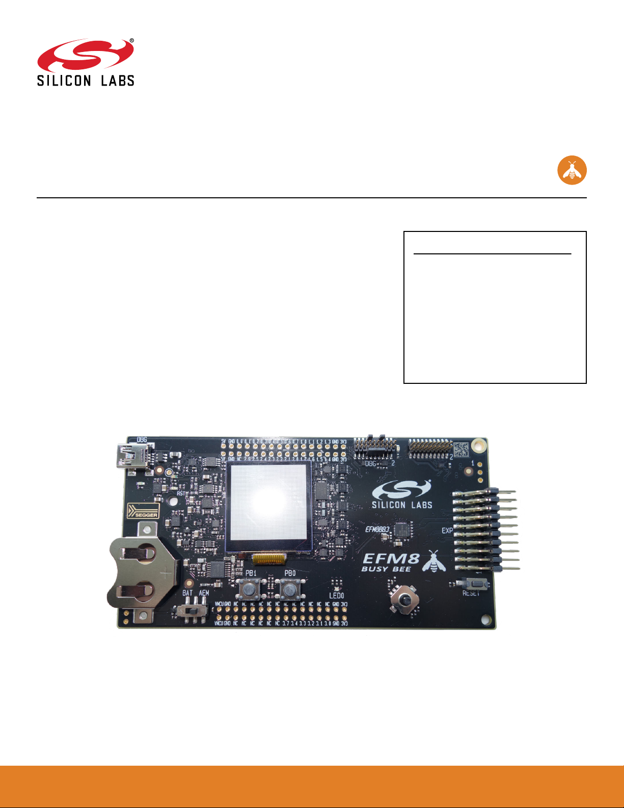
• EFM8BB3 Busy Bee Starter Kit Board
• 1 x CR2032 battery
• Getting Started card
• 1 x mini USB cable
KEY FEATURES
• EFM8BB31F64G MCU with 64 KB Flash
and 4 KB RAM.
• 20-pin expansion header.
• Power sources include USB and CR2032
battery.
• 2 user buttons, 1 tri-color LED.
• 8-direction joystick.
• Ultra low power 128x128 pixel MemoryLCD.
silabs.com | Building a more connected world. Rev. 0.7
Page 2
UG125: EFM8BB3-SLSTK2022A User's Guide
Getting Started
1. Getting Started
For information on getting started with the EFM8BB3-SLSTK2022A kit, including links to documentation and other resources, visit the
kit product page.
Hardware
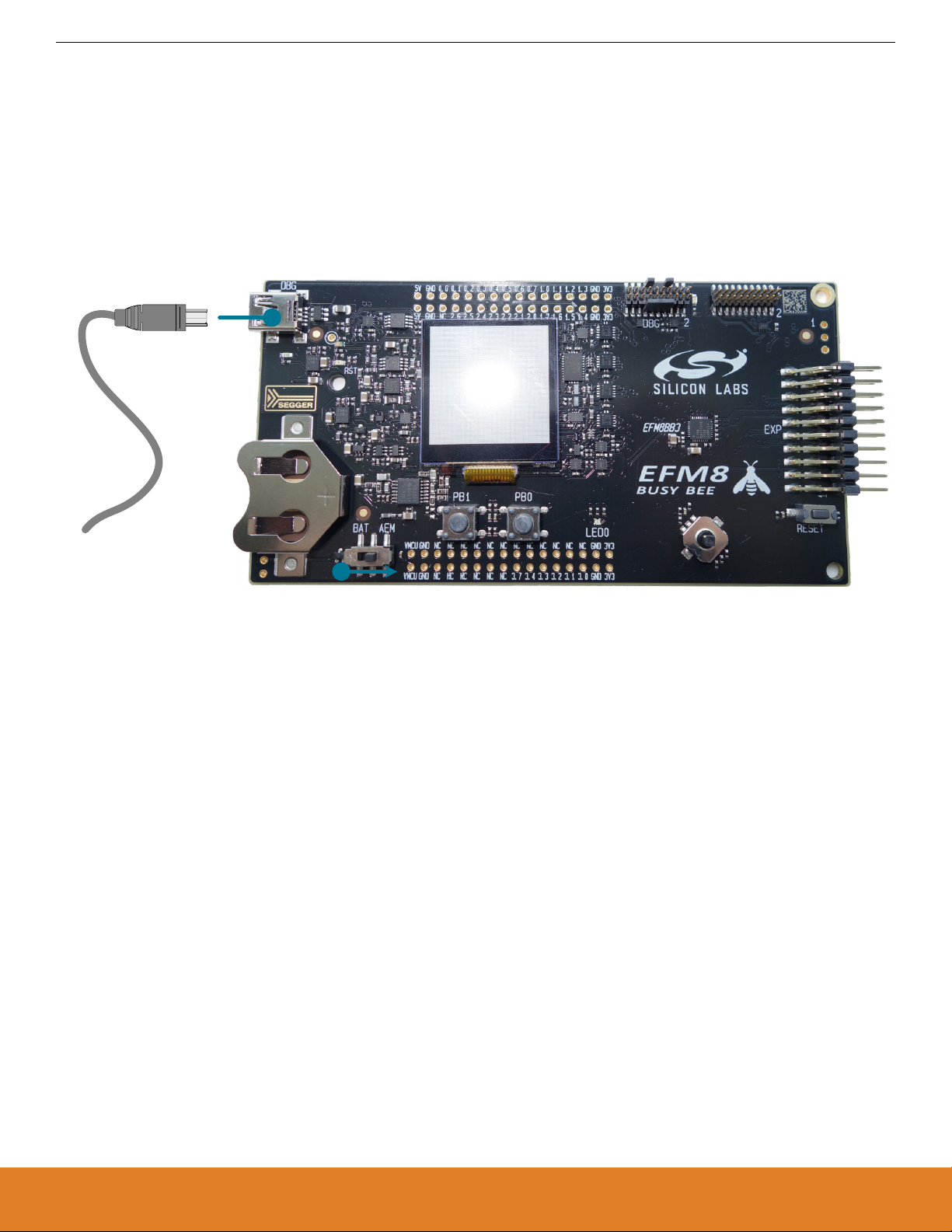
To set up the hardware for the EFM8BB3-SLSTK2022A kit:
1. Provide power to the board by connecting the USB connector to the PC using the provided USB cable.
2. Move the switch to the Advanced Energy Monitor (AEM) position.
Figure 1.1. Hardware Setup
Software
The first step to get started with your new EFM8BB3-SLSTK2022A is to go to http://www.silabs.com/simplicity.
The Simplicity Studio software package contains all the tools, drivers, software examples and documentation needed to use the
EFM8BB3 Starter Kit. The board comes pre-loaded with a default application, Space Invaders, to interact with while the software downloads.
After downloading the latest version of Simplicity Studio:
1. Select the J-Link adapter for the kit under [Devices].
2. Click one of the demos available under [Getting Started]>[Demos] or click the [Getting Started]>[Demos]>[View All] to view the
entire list of available demos.
3. Click the [Space Invaders] demo and click [Start] to download and run the demo.
Additional demos showcasing the various features of the EFM8 are also available in Simplicity Studio.
silabs.com | Building a more connected world. Rev. 0.7 | 2
Page 3
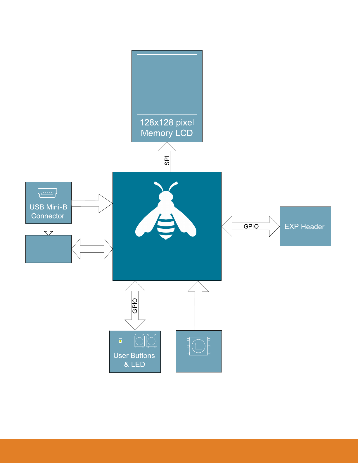
2. Kit Block Diagram
ADC
Joystick
EFM8BB3
Microcontroller
POWER
Board
Controller
UART
An overview of the EFM8BB3 Starter Kit is shown in the figure below.
UG125: EFM8BB3-SLSTK2022A User's Guide
Kit Block Diagram
Figure 2.1. Kit Block Diagram
silabs.com | Building a more connected world. Rev. 0.7 | 3
Page 4
3. Kit Hardware Layout
Kit USB
Connector
CR2032
Battery Holder
Power Source Select
User Push
Buttons
User LED
EFM8 Reset Button
EFM8BB3 MCU
Expansion
Header
Joystick
128x128 Pixel
Memory LCD
Direct
Debug Connector
Debug IN/OUT
Connector
Reference
Board Connector
The layout of the EFM8BB3 Starter Kit is shown below.
UG125: EFM8BB3-SLSTK2022A User's Guide
Kit Hardware Layout
The EFM8 device on the kit is connected to several peripherals. The table below shows all of the external connections to the MCU.
Figure 3.1. EFM8BB3-SLSTK2022A Hardware Layout
Table 3.1. Kit MCU Connections
MCU Port Pin Port Pin Assigned
Function
P0.0 GPIO VREF Caps
P0.1 GPIO AGND
P0.2 Port Match Input Push Button 0 (PB0)
Primary Board Connection
Secondary Board Connection
Expansion Port Connection (EXP)
P0.3 Port Match Input Push Button 1 (PB1)
P0.4 UART0 TX BC - UART_TX
P0.5 UART0 RX BC - UART_RX
P0.6 SPI0 SCK
P0.7 SPI0 MISO SPI MISO EXP6
P1.0 SPI0 MOSI DISP - SPI MOSI SPI MOSI EXP4
P1.1 SPI0 NSS SPI CS EXP10
P1.2 SMBus0 SDA I2C SDA BC - REFCLK EXP16
DISP - SPI CLK
1
SPI CLK EXP8
P1.3 SMBus0 SCL I2C SCL BC - 1 kHz SINE EXP15
P1.4 PCA0 CEX0 RGB LED0
P1.5 PCA0 CEX1 RGB LED1
P1.6 PCA0 CEX2 RGB LED2
silabs.com | Building a more connected world. Rev. 0.7 | 4
Page 5
UG125: EFM8BB3-SLSTK2022A User's Guide
Kit Hardware Layout
MCU Port Pin Port Pin Assigned
Function
Primary Board Connection
Secondary Board Connection
Expansion Port Connection (EXP)
P1.7 ADC / CMP Joystick
P2.0 UART1 TX UART1 TX EXP12
P2.1 UART1 RX UART1 RX EXP14
P2.2 GPIO BC - Enable
P2.3 GPIO DAC LOOPBACK0 EXP3
P2.4 GPIO EXP13
P2.5 GPIO UFL ADC INPUT
P2.6 GPIO DISP - SPI CS
P3.0 GPIO DAC LOOPBACK1 EXP5
P3.1 GPIO EXP7
P3.2 GPIO EXP9
P3.3 GPIO EXP11
P3.4 GPIO DISP - Enable
P3.7 / C2D C2D (for debug)
Note:
1. This signal has high loading. If the MCU pin is used for signals where edge speed is critical, this signal should be disconnected
from the pin.
silabs.com | Building a more connected world. Rev. 0.7 | 5
Page 6
UG125: EFM8BB3-SLSTK2022A User's Guide
Power Supply and Reset
4. Power Supply and Reset
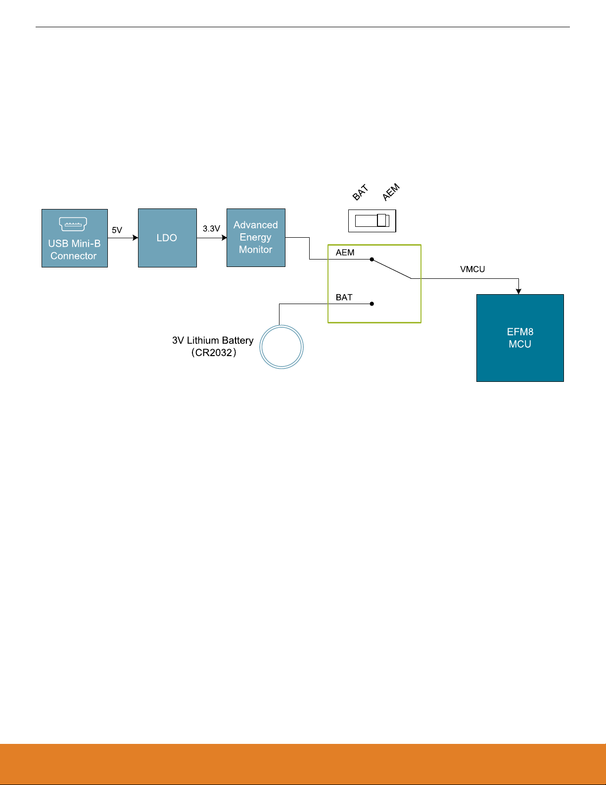
4.1 MCU Power Selection
The Busy Bee MCU on the EFM8BB3-SLSTK2022A is designed to be powered by three different sources:
• Through the on-board debugger.
• By a 3 V battery.
• By an externally supplied power source.
Selecting the power source is done with the slide switch in the lower left corner of the board. The figure shows how the different power
sources can be selected with the slide switch.
Figure 4.1. EFM8BB3-SLSTK2022A Power Switch
With the switch in the AEM position, an on-board low noise LDO with a fixed output voltage of 3.3 V is used to power the MCU. This
LDO is powered from the "J-Link" USB cable.
With the switch in the BAT position, the device may be powered from either a 20 mm coin cell battery (in the CR2032 socket) or an
external power supply (connected to the VMCU and GND pins on the expansion header).
4.2 MCU Reset
The EFM8 MCU can be reset by a few different sources:
• The RESET button.
• An external debugger by pulling the RSTb pin low.
silabs.com | Building a more connected world. Rev. 0.7 | 6
Page 7

UG125: EFM8BB3-SLSTK2022A User's Guide
Peripherals
5. Peripherals
The starter kit has a set of peripherals that showcase some of the features of the EFM8 Busy Bee microcontroller.
Be aware that most EFM8 I/O routed to peripherals are also routed to the breakout pads. This must be taken into consideration when
using the breakout pads for your application.
5.1 Push Buttons and LEDs
The kit has two user push buttons. They are connected to the EFM8, and are debounced by RC filters with a time constant of 1 ms. The
buttons are connected to pins P0.2 and P0.3.
In addition to the two push buttons, the kit also features a tri-color LED that is controlled by EFM8 GPIO. The LED is connected to pins
P1.4, P1.5, and P1.6 in an active-low configuration.
Figure 5.1. Buttons/LEDs
silabs.com | Building a more connected world. Rev. 0.7 | 7
Page 8

UG125: EFM8BB3-SLSTK2022A User's Guide
Peripherals
5.2 Joystick
The kit has an analog joystick with 8 measureable positions. This joystick is connected to the EFM8 on the P1.7 pin and uses different
resistor values to create voltages measurable by the ADC0.
Figure 5.2. Joystick
Table 5.1. Joystick Resistor Combinations
Direction Resistors Combinations (kΩ)
Center press
Up (N)
Up-Right (NE)
Right (E)
Down-Right (SE)
Down (S)
Down-Left (SW)
Left (W)
Up-Left (NW)
(N // E )
(N // E ) + 10
(S // E )
(S // E ) + 10
(S // W ) + 10
(N // W )
(N // W ) + 10
0.1
60.4 + 10
33
10
(S // W )
15
0.1
+ 10
60.4
=
33
+ 10
10
+ 10
15
+ 10
21.34
21.34 + 10
7.67
=
7.67 + 10
=
6 + 10
12.01
=
12.01 + 10
6
Note:
1. These calculated values assume a VMCU of 3.3 V.
Expected UIF_JOYSTICK Voltage (V)
0.033
2.831
2.247
2.533
1.433
1.650
1.238
1.980
1.801
1
silabs.com | Building a more connected world. Rev. 0.7 | 8
Page 9

0: BC controls display
1: EFM controls display
EFM_DISP_ENABLE
8
P0.6 (SPI0)
P1.0 (SPI0)
P2.6 (GPIO)
P3.4 (GPIO)
UG125: EFM8BB3-SLSTK2022A User's Guide
Peripherals
5.3 Memory LCD-TFT Display
A 1.28-inch SHARP Memory LCD-TFT has been added to the board to enable interactive applications to be developed. The display has
a high resolution of 128 by 128 pixels and consumes very little power. It is a reflective monochrome display, so each pixel can only be
light or dark, and no backlight is needed in normal daylight conditions.
The display interface consists of a SPI-compatible serial interface and some extra control signals. Data are sent to the display one line
(128 bits) at a time.
The Memory LCD-TFT display is shared with the kit Board Controller, allowing the Board Controller application to display useful information when the user application is not using the display. The EFM8 MCU always controls ownership of the display using the
EFM_DISP_ENABLE signal:
• 0: The Board Controller has control of the display.
• 1: The user application (EFM8) has control of the display.
Data are clocked in on EFM_DISP_MOSI (P1.0) when EFM_DISP_CS (P2.6) is high, and the clock is sent on EFM_DISP_SCLK
(P0.6). The maximum supported clock speed is 1 MHz.
Refer to the display application information for details on driving the display:
http://www.sharpmemorylcd.com/1-28-inch-memory-lcd.html
Figure 5.3. 128x128 Pixel Memory LCD
silabs.com | Building a more connected world. Rev. 0.7 | 9
Page 10

UG125: EFM8BB3-SLSTK2022A User's Guide
Connectors
6. Connectors
6.1 Breakout Pads
Many of the EFM8's pins are routed out to "breakout pads" at the top and bottom edges of the kit. A 2.54 mm pitch pin header can be
soldered in for easy access to these pins. Most I/O pins are available, with the exception of pins used to drive the LCD.
Note: Some of the breakout pads are shared by on-board EFM peripherals. The schematic must be consulted to make sure that it is
acceptable to use a shared pin in your application.
Figure 6.1. Breakout Pads and Expansion Header
silabs.com | Building a more connected world. Rev. 0.7 | 10
Page 11

UG125: EFM8BB3-SLSTK2022A User's Guide
Connectors
6.2 Expansion Header
On the right hand side of the board an angled 20-pin expansion header is provided to allow connection of peripherals or plugin boards.
The connecter contains a number of I/O pins that can be used with most of the Busy Bee's features. Additionally, the VMCU, 3V3 and
5V power rails are also exported.
The figure below shows the pin assignment of the expansion header. With the exception of a few pins, most of the expansion header's
pins are the same as those on the EFM32 Gecko or EFM32 Tiny Gecko starter kits.
Figure 6.2. Expansion Header
Some of the chip peripheral functions that are available on the expansion header are listed in the table below.
Table 6.1. Some Peripheral Functions Available on Expansion Header
Peripheral Peripheral pin MCU Pin EXP Header pin
number
UART1 UART1 TX P2.0 12
UART1 RX P2.1 14
SPI0 SPI0 SCK P0.6 8
SPI0 MISO P0.7 6
SPI0 MOSI P1.0 4
SPI0 CS P1.1 10
SMBus SMBus0 SDA P1.2 16
SMBus0 SCL P1.3 15
I2CSLAVE0 I2CSLAVE0 SDA P2.0 12
I2CSLAVE0 SCL P2.1 14
ADC0 Input Any supported pin (see Reference Manual for more information) Multiple
CNVSTR P0.6 8
Comparator 0 CMP0P Positive Input Any supported pin (see Reference Manual for more information) Multiple
CMP0N Negative In-
Any supported pin (see Reference Manual for more information) Multiple
put
Comparator 1 CMP1P Positive Input Any supported pin (see Reference Manual for more information) Multiple
CMP1N Negative In-
Any supported pin (see Reference Manual for more information) Multiple
put
silabs.com | Building a more connected world. Rev. 0.7 | 11
Page 12

UG125: EFM8BB3-SLSTK2022A User's Guide
Connectors
Note: This table only sums up some of the alternate functions available on the expansion header. Consult the EFM8BB31F64G data
sheet for a complete list of alternate functions.
6.3 Debug Connector
This connector is used for Debug In and Debug Out (see chapter on Debugging).
Figure 6.3. Debug Connector
Table 6.2. Debug Connector Pinout
Pin num-
Function Note
ber
1 VTARGET Target voltage on the debugged application.
Note: This connection is required and is needed for the debug circuitry to match voltage levels
with the target device.
2 TMS/SWDIO/C2D JTAG TMS, Serial Wire data I/O, or EFM8 C2 data I/O
4 TCK/SWCLK/C2CK JTAG TCK, Serial Wire clock, or EFM8 C2 clock
6 TDO/SWO JTAG TDO or Serial Wire output
8 TDI JTAG data in
9 ATTACH This signal must be pulled to ground by the external debugger or application for cable insertion
detection.
10 #RESET Target MCU reset.
12 TRACECLK Trace clock
14, 16,
TRACED0-3 Trace data (4 lines)
18, 20
11, 13 NC Not Connected
3, 5, 15,
GND
17, 19
silabs.com | Building a more connected world. Rev. 0.7 | 12
Page 13

UG125: EFM8BB3-SLSTK2022A User's Guide
Connectors
6.4 Direct Debug Connector
This connector (J103) is used for directly debugging the EFM8 using an external debug adapter (see chapter on Debugging). This is
especially useful for debugging the MCU on the STK board when the part is battery powered or powered by an external supply.
Figure 6.4. Direct Debug Connector
Table 6.3. Direct Debug Connector Pinout
Pin number Function Note
1 C2CK EFM8 C2 clock
2 C2D EFM8 C2 data I/O
3 GND
6.5 Reference Board
The top right corner of the board includes a 20-pin reference board connector. The connecter contains some I/O pins that can be used
with some of the EFM8 Busy Bee's features. Additionally, the 3V3 and 5V power rails are also exported.
The figure below shows the pin assignment of the reference board header.
Figure 6.5. Reference Board Header
silabs.com | Building a more connected world. Rev. 0.7 | 13
Page 14

UG125: EFM8BB3-SLSTK2022A User's Guide
Advanced Energy Monitor
7. Advanced Energy Monitor
7.1 Usage
The AEM data is collected by the board controller and can be displayed by the energyAware Profiler, available through Simplicity Studio. By using the energyAware Profiler, current consumption and voltage can be measured in realtime.
7.2 Theory of Operation
To accurately measure current ranging from 0.1 µA to 50 mA (114 dB dynamic range), a current sense amplifier is utilized together with
a dual gain stage. The current sense amplifier measures the voltage drop over a small series resistor, and the gain stage further amplifies this voltage with two different gain settings to obtain two current ranges. The transition between these two ranges occurs around
250 µA. Digital filtering and averaging is done within the Board Controller before the samples are exported to the Energy Profiler application.
During startup of the kit, an automatic calibration of the AEM is performed. This calibration compensates for the offset error in the sense
amplifiers.
Figure 7.1. Advanced Energy Monitor
7.3 Accuracy and Performance
The AEM is capable of measuring currents in the range of 0.1 µA to 47 mA. For currents above 250 µA, the AEM is accurate within 0.1
mA. When measuring currents below 250 µA, the accuracy increases to 1 µA. Although the absolute accuracy is 1 µA in the sub 250
µA range, the AEM is able to detect changes in the current consumption as small as 100 nA. The AEM produces 6250 current samples
per second.
silabs.com | Building a more connected world. Rev. 0.7 | 14
Page 15

UG125: EFM8BB3-SLSTK2022A User's Guide
Board Controller
8. Board Controller
The kit contains a board controller that is responsible for performing various board-level tasks, such as handling the debugger and the
Advanced Energy Monitor. An interface is provided between the EFM8 and the board controller in the form of a UART connection. The
connection is enabled by setting the EFM_BC_EN (P2.2) line high, and using the lines EFM_BC_TX (P0.4) and EFM_BC_RX (P0.5) for
communicating.
The BC enable signal connects the EFM8 to the board controller:
• 0: EFM8 UART pins are isolated from the Board Controller.
• 1: EFM8 UART pins are connected to the Board Controller (default upon reset).
Note: The board controller is only available when USB power is connected.
silabs.com | Building a more connected world. Rev. 0.7 | 15
Page 16

UG125: EFM8BB3-SLSTK2022A User's Guide
Debugging
9. Debugging
The EFM8BB3-SLSTK2022A contains an integrated debugger, which can be used to download code and debug the Busy Bee EFM8
MCU. In addition to programming the MCU on the kit, the debugger can also be used to program and debug external Silicon Labs
EFM8 devices.
9.1 Debug Modes
Programming external devices is done by connecting to a target board through the provided Debug IN/OUT Connector, and by setting
the debug mode to [Out]. The same connector can also be used to connect an external debugger to the EFM8 MCU on the kit by setting the debug mode to [In]. A summary of the different supported debug modes is given in the following table.
Table 9.1. Debug Modes
Mode Description
Debug MCU In this mode, the on-board debugger is connected to the EFM8 on the EFM8BB3-SLSTK2022A.
Debug In In this mode, the on-board debugger is disconnected and an external debugger can be connected to debug the
EFM8 on the EFM8BB3-SLSTK2022A.
Debug Out In this mode, the on-board debugger can be used to debug an EFM8 mounted on a custom board.
Selecting the active debug mode is done with a drop-down menu in the Kit Manager tool, which is available through Simplicity Studio.
When using the debug adapter in the [Out] mode, the end device must be manually detected before debugging and programming. To
do this:
1. Right-click on the kit from the Simplicity Studio launch screen and select [Select Target Part...].
2. If needed, select the appropriate [Target Interface] for the external device. For example, EFM8 devices will use the [C2] selection.
3. In the same dialog, click the [Detect Target] button.
4. Click [OK] to close the dialog. The external target can now be debugged and programmed.
9.2 Debugging during Battery Operation
When the EFM8 is powered by battery and the J-Link USB is still connected, the on-board debug functionality is available. If the USB
power is disconnected, the Debug In mode will stop working.
To enable debugging when the USB cable is removed, connect an external debugger to the MCU Debug Header in the top right corner
of the EFM8BB3-SLSTK2022A instead of the Debug IN/OUT Connector. This header is connected directly to the EFM8's debug interface. The pinout of this header is shown in the Connectors chapter.
silabs.com | Building a more connected world. Rev. 0.7 | 16
Page 17

UG125: EFM8BB3-SLSTK2022A User's Guide
Kit Configuration and Upgrades
10. Kit Configuration and Upgrades
The kit configuration dialog in Simplicity Studio allows you to change the J-Link adapter debug mode, upgrade its firmware, and change
other configuration settings. To download Simplicity Studio, go to http://www.silabs.com/simplicity.
In the main window of the Simplicity Studio's Launcher perspective, the debug mode and firmware version of the selected J-Link adapter are shown. Click the [Change] link next to any of them to open the kit configuration dialog.
Figure 10.1. Simplicity Studio Kit Information
Figure 10.2. Kit Configuration Dialog
10.1 Firmware Upgrades
Upgrading the kit firmware is done through Simplicity Studio. Simplicity Studio will automatically check for new updates on startup.
You can also use the kit configuration dialog for manual upgrades. Click the [Browse] button in the [Update Adapter] section to select
the correct file ending in .emz. Then, click the [Install Package] button.
silabs.com | Building a more connected world. Rev. 0.7 | 17
Page 18

UG125: EFM8BB3-SLSTK2022A User's Guide
Schematics, Assembly Drawings, and BOM
11. Schematics, Assembly Drawings, and BOM
The schematics, assembly drawings, and bill of materials (BOM) for the EFM8BB3 Starter Kit board are available through Simplicity
Studio when the kit documentation package has been installed.
11.1 Board Revision History
• A00 — Initial prototype revision.
• A01 — Cleaned up the signal generator circuit and updated silk print.
• A02 — Updated EFM8BB3 device revision and adjusted the reset switch.
• A03 — Changed D801 to “not mounted”. Changed X900 to KDS DSX321G.
• A04 — Updated EFM8BB3 device revision.
• A05 — Updated EFM8BB3 device revision. Updated end-of-life blue LED.
A00 Revision Boards
There are no known issues with the A00 boards.
A01 Revision Boards
There are no known issues with the A01 boards.
A02 Revision Boards
There are no known issues with the A02 boards.
A03 Revision Boards
There are no known issues with the A03 boards.
A04 Revision Boards
There are no known issues with the A04 boards.
A05 Revision Boards
There are no known issues with the A05 boards.
silabs.com | Building a more connected world. Rev. 0.7 | 18
Page 19

12. Revision History
Revision 0.7
September, 2020
• Updated 11.1 Board Revision History for Rev A05
• Updated the AEM section.
Revision 0.6
February, 2019
• Updated 11.1 Board Revision History for Rev A04
Revision 0.5
April, 2018
• Updated 6.1 Breakout Pads with the correct pin numbers for J101 and J102.
• Updated 11.1 Board Revision History for Rev A03.
Revision 0.4
UG125: EFM8BB3-SLSTK2022A User's Guide
Revision History
January, 2018
• Updated 6.2 Expansion Header with the correct pin label for EXP13.
Revision 0.3
June, 2016
• Updated screenshots and instructions for Simplicity Studio v4.
• Added 11.1 Board Revision History.
• Added the UG125 document reference.
• Added a note to 6.3 Debug Connector that VTARGET is required.
• Added the reference for the direct debug connector to 6.4 Direct Debug Connector.
• Added a note about high loading on the DISP CLK signal.
Revision 0.2
September, 2015
• Updated board pictures.
Revision 0.1
June, 2015
• Initial revision.
silabs.com | Building a more connected world. Rev. 0.7 | 19
Page 20

Simplicity Studio
One-click access to MCU and wireless
tools, documentation, software, source
code libraries & more. Available for
Windows, Mac and Linux!
IoT Portfolio
www.silabs.com/IoT
Disclaimer
Silicon Labs intends to provide customers with the latest, accurate, and in-depth documentation of all peripherals and modules available for system and software implementers using or
intending to use the Silicon Labs products. Characterization data, available modules and peripherals, memory sizes and memory addresses refer to each specific device, and “Typical”
parameters provided can and do vary in different applications. Application examples described herein are for illustrative purposes only. Silicon Labs reserves the right to make changes
without further notice to the product information, specifications, and descriptions herein, and does not give warranties as to the accuracy or completeness of the included information.
Without prior notification, Silicon Labs may update product firmware during the manufacturing process for security or reliability reasons. Such changes will not alter the specifications or
the performance of the product. Silicon Labs shall have no liability for the consequences of use of the information supplied in this document. This document does not imply or expressly
grant any license to design or fabricate any integrated circuits. The products are not designed or authorized to be used within any FDA Class III devices, applications for which FDA
premarket approval is required, or Life Support Systems without the specific written consent of Silicon Labs. A “Life Support System” is any product or system intended to support or
sustain life and/or health, which, if it fails, can be reasonably expected to result in significant personal injury or death. Silicon Labs products are not designed or authorized for military
applications. Silicon Labs products shall under no circumstances be used in weapons of mass destruction including (but not limited to) nuclear, biological or chemical weapons, or
missiles capable of delivering such weapons. Silicon Labs disclaims all express and implied warranties and shall not be responsible or liable for any injuries or damages related to use of
a Silicon Labs product in such unauthorized applications.
Trademark Information
Silicon Laboratories Inc.®, Silicon Laboratories®, Silicon Labs®, SiLabs® and the Silicon Labs logo®, Bluegiga®, Bluegiga Logo®, ClockBuilder®, CMEMS®, DSPLL®, EFM®,
EFM32®, EFR, Ember®, Energy Micro, Energy Micro logo and combinations thereof, “the world’s most energy friendly microcontrollers”, Ember®, EZLink®, EZRadio®, EZRadioPRO®,
Gecko®, Gecko OS, Gecko OS Studio, ISOmodem®, Precision32®, ProSLIC®, Simplicity Studio®, SiPHY®, Telegesis, the Telegesis Logo®, USBXpress®, Zentri, the Zentri logo and
Zentri DMS, Z-Wave®, and others are trademarks or registered trademarks of Silicon Labs. ARM, CORTEX, Cortex-M3 and THUMB are trademarks or registered trademarks of ARM
Holdings. Keil is a registered trademark of ARM Limited. Wi-Fi is a registered trademark of the Wi-Fi Alliance. All other products or brand names mentioned herein are trademarks of
their respective holders.
Silicon Laboratories Inc.
400 West Cesar Chavez
Austin, TX 78701
USA
http: //www.silabs.com
SW/HW
ww.silabs.com/simplicity
w
Quality
ww.silabs.com/quality
w
Support & Community
abs.com/community
www.sil
 Loading...